
 Open Access Article
 This Open Access Article is licensed under a Creative Commons Attribution-Non Commercial 3.0 Unported Licence
A self-powered photodetector through facile processing using polyethyleneimine/carbon quantum dots for highly sensitive UVC detection†
Vo Pham Hoang Huy and
Chung Wung Bark *
*
Department of Electrical Engineering, Gachon University, Seongnam, Gyeonggi 13120, Republic of Korea. E-mail: bark@gachon.ac.kr
First published on 17th April 2024
Abstract
Ultraviolet C (UVC) photodetectors have garnered considerable attention recently because the detection of UVC is critical for preventing skin damage in humans, monitoring environmental conditions, detecting power aging in facilities, and military applications. As UVC detectors are “solar-blind”, they encounter less interference than other environmental signals, resulting in low disturbance levels. This study employed a natural precursor (glucose) and a one-step ultrasonic reaction procedure to prepare carbon quantum dots (CQDs), which served as a convenient and environmentally friendly material to combine with polyethyleneimine (PEI). The prepared materials were used to develop a self-powered, high-performance UVC photodetector. The thickness of the constitutive film was investigated in detail based on the conditions of the electron transport pathway and trap positions to further improve the performance of the PEI/CQD photodetectors. Under the optimized conditions, the photodetector could generate a strong signal (1.5 mA W−1 at 254 nm) and exhibit high detectability (1.8 × 10¹⁰ Jones at 254 nm), an ultrafast response, and long-term stability during the power supply sequence. The developed solar-blind UVC photodetector can be applied in various ways to monitor UVC in an affordable, straightforward, and precise manner.
1. Introduction
Although the ultraviolet (UV) region comprises 10% of the total solar radiation, it has an immense effect on ecosystems, including human life. UV light is extensively used in many fields, including polymer curing in semiconductor fabrication, lithography, subcutaneous exploration in the medical field, germ sterilization, air disinfection, and flare detection in military applications.1,2 The detection of UV C-band (UVC) or deep-UV emissions can potentially be used as a predictive warning signal for corona discharge or flame detection, which is essential for human safety. UVC exposure is extremely high for arc welders and scientists who operate with open arc and specialized arc lamps. There has been considerable interest in monitoring the UVC levels in these specialized areas. Furthermore, increasing UVC radiation may affect residential areas because of ozone layer depletion. It is generally known that even at extremely low exposure levels, UVC can have a significantly negative impact, which is typically manifested as acute and chronic dermatitis.3–6 For instance, Trevisan et al. reported that acute exposure to short wavelengths (245–290 nm) can damage mammalian cells at the DNA level.7 Abnormal skin reactions have been observed in welders.8 Acute sunburn was reported when using electricity to kill insects with equipment that emitted up to 46 mW m−2 of radiation.9 Nevertheless, it is difficult to perceive low-intensity UVC light in surroundings lit with ordinary visible light (sunlight). Thus, it is critical to develop a sensitive photodetector (PD) to monitor UVC radiation during daylight hours.10–12In recent years, wide bandgap semiconductors (Eg > 4.43 eV), such as AlGaN, MgZnO, β-Ga2O3, GaN, NiO, BN, and LaAlO3, have been increasingly used to detect solar-blind UV. Studies related to UVC detectors and their respective performance are presented in Table 1. These materials have demonstrated high sensitivity,13–15 flexible detection,16 and operation in severe conditions.17 Unfortunately, the production techniques for these PDs are intricate and expensive, and the lattice mismatch between the film and the substrate is often a concern for their applications.18 Besides, the bandgap of a semiconductor must surpass 4.4 eV to detect UVC light, which greatly limits the choices of semiconductor materials.19 Therefore, finding suitable materials and simple manufacturing techniques are critical challenges for fabricating high-performance PDs. Organic photodetectors (OPDs) have garnered significant attention for the upcoming era of flexible electronics owing to their potential as flexible and lightweight PDs. OPDs have high photodetection capabilities and can be easily tuned to achieve specific optoelectronic features, such as charge production, transport, and recombination, by adjusting their molecular architectures.20 Another advantage of OPDs is that their detection band (wavelength range) can be easily controlled by altering the organic active materials. Moreover, OPDs are solution-processable, and the printable electroactive inks enable large-scale, low-cost manufacture on flexible substrates.21–23 More significantly, human tissue has an approximate average density of 1.10 g cm−3, with soft tissues frequently targeted in medical dosimetry having a density of 1.07 g cm−3. Thus, the density of thin solid films made from organic electroactive inks is very similar to that of human tissue.24 Because of these benefits, organic electronic materials have become increasingly popular in a wide range of applications, such as thin-film transistors,25 solar cells,26–28 sensors,29 visual displays,30 PDs,31 and the medical devices.32 According to a recent study on polymer-based UV PDs, organic semiconductors produce good UV PDs owing to their selectivity and sensitivity at the wavelengths required for diverse applications.33–38 The advantages of all-organic UV PDs include straightforward processing methods, inexpensive material costs, functional tunability, and the ability to process on flexible substrates.39–42 The chemical and physical features of organic materials can be modified to reinforce their bandgap and adjust their chemical composition for more UV absorption. Selecting materials with excellent absorption properties and an internal network of donors and acceptors can effectively convert photons to electrons, boost the mobility of the high-charge carriers,43 and create more stable charge carriers among the thin solid films. Active organic layers with bulk heterojunctions formed by blending hole-transporting and electron-transporting materials are typically utilized in device manufacturing. Conductive polymers have found extensive applications in UV PDs, supercapacitors, batteries, and electrochemical detection owing to their high transmittance in the UV-vis region, excellent hole transport capacity, straightforward processing, conjugated π-electrons, excellent flexibility, favorable stability, amenability to deposition by solution-processing, and low material cost. Consequently, conjugated polymers are recognized as prospective candidate materials for combining n-type semiconductors and p–n heterojunction solar devices.44
| Photo-absorbing materials | Voltage (V) | Wavelength (nm) | Responsivity (mA W−1) | Detectivity (Jones) | Thickness (nm) | Ref. |
|---|---|---|---|---|---|---|
| AlGaN | 20 | 269 | 2.34 × 10³ | — | 600 | 64 |
| MgZnO | — | 254 | 0.22 | 4.00 × 10¹⁰ | 20 | 65 |
| Ga2O3 | 5 | 260 | 2.4 × 10¹⁰ | 1.70 × 10¹⁵ | 270 | 66 |
| ZnGa2O4 | 5 | 233 | 86.3 × 10³ | 2.45 × 10⁸ | — | 67 |
| BN | 20 | 212 | 0.1 | 2.4 × 10⁸ | 3 | 68 |
| LaAlO3 | 10 | 210 | 71.8 | — | 500 | 69 |
| In2Ge2O7 | 3.0 | 290 | 3.9 × 10⁸ | — | 30 | 70 |
| CuO | 0.2 | 280 | 1.03 × 10⁴ | — | 45 | 71 |
| CsPbBr3 | −0.1 | 279 | 1.4 | 2.4 × 10¹¹ | 103 | 72 |
| ZnS QD | 15 | 254 | 1.6 | 0.55 × 10¹⁰ | — | 73 |
| ZnS QD | 40 | 265 | 0.1 | — | 130 | 74 |
| NiO | 0.05 | 250 | — | 2.44 × 10¹¹ | 150 | 75 |
| ZnS QD | Self-power | 250 | 0.29 | 1.41 × 10¹⁰ | 315 | 18 |
| GaN | Self-power | 244 | 14.9 | 8.1 × 10¹¹ | 3 × 10³ | 76 |
| SnO2 QD | Self-power | 254 | 49.6 | 2.16 × 10¹⁰ | 111 | 19 |
Among different conductive polymers, polyethyleneimine (PEI) is an inexpensive and accessible polymer that can modify the nucleation of ZnO nanorods on a polycrystalline ZnO seed layer, thus modifying the aspect ratio of ZnO nanorods. PEI can be adsorbed on ZnO in an orientation with the m-planes parallel to the surface, which slows the nucleation rate of ZnO and causes a sizable vertical misalignment.45 Ultralong ZnO nanorods can be achieved by adding PEI to the solution used for standard hydrothermal synthesis. Qiu et al. generated ∼40 μm long, vertically aligned ZnO nanorod arrays after numerous growth cycles using a PEI-assisted preheating hydrothermal technique.46 Burke-Govey et al. controlled the diameter and length of ZnO nanowires using PEI with distinct molecular weights at various concentrations.47 Additionally, Chen et al. attached PEI to modify the structural and optical characteristics of ZnO nanowires and established a connection between the visible emissions and structural defects in ZnO nanowires.48 Zhou et al. were the first to employ aliphatic amine-rich polymers like PEI as surface modifiers for modulating electrical interactions.49 The presence of PEI improved the power detection boundary and specific detection ability by lowering the dark current of the device. Cesarini et al. used non-toxic solvents instead of 2-methoxyethanol to print PEI on different substrates,50 and the effects of different parameters used for depositing PEI interlayer on the repeatability of the performance of the inkjet-printed devices were studied. The use of multiple solvents significantly increased the yield (from less than 20% to more than 90%). Furthermore, the dark current was lowered to 57 nA cm−2. Because of the interface between the PEI interlayer and the photoactive layer, these devices also had faster response times of up to 30 s. Despite the numerous advantages of PEI-based devices, the combination of PEI and organic compounds has rarely been investigated.
Carbon quantum dots (CQDs) have received widespread attention from the scientific community owing to their promising photoluminescence and electronic properties. CQDs have found wide applications in light-emitting diodes,51 chemical sensors,52 photocatalysts,53–55 fluorescent probes,56,57 optical sensitizers,58 photovoltaics,59 and DNA detection.60 In contrast to compound semiconductors, such as perovskites, silicon, germanium, and gallium arsenide, all forms of carbon-based materials have unique environmental benefits, including earth-abundance, low toxicity, chemical stability, and biocompatibility. CQDs have been investigated as photosensitive materials for photodetection applications in several anchored or hybrid architectures. The zero-dimensional confinement exhibited by quantum dots facilitates inter-sub-band transitions between quantized energy levels, thereby enabling broadband photodetection. Lee et al. explored a ZnO nanorod/CQD composite as a feasible PD and found that CQDs could act as an electron–hole separator when exposed to UV light.61 Similarly, Li et al. employed CQDs to separate the excitons produced by photosynthesis in TiO2 to reduce the dark current and increase the reaction time.62 Furthermore, Sahatiya et al. created a hybrid structure using CQDs and MoS2 on a glass substrate, which could be used for broadband photodetection from the UV to near-infrared (NIR) region. CQDs demonstrate the advantages of high mobility of photogenerated carriers, tunable bandgaps, ability to function as both an electron donor and an acceptor, high molar extinction coefficients and light absorption coefficients, and wide absorption wavelength ranges. However, CQD-based PDs have been scarcely reported because of their low responsiveness and slow reaction speed.63
In this study, a UVC PD with an intrinsically wide bandgap is fabricated using CQDs and PEI. A straightforward spin-coating process is used to prepare the PD with an asymmetric pair of Schottky contacts, including PEI-coated fluorine-doped tin oxide (FTO)/CQD and poly(3,4-ethylenedioxythiophene):polystyrene sulfonate (PEDOT:PSS)/CQD. The as-fabricated device demonstrates a satisfactory response to 254 nm UV radiation with a self-powered function. The CQD-based PD also showed a high response (1.5 mA W−1 at 254 nm), high detection ability (1.8 × 10¹⁰ Jones at 254 nm), and an ultrafast response time. Moreover, after 50 cycles, the photo-response of the unencapsulated UVC PD remains consistent. The CQDs improve the conductivity of the composite for carrier transport by reducing the interfacial trap states in the heterojunction. The recommended device design utilizes CQDs in conjunction with PEI. These components can be readily combined on an FTO substrate using simple fabrication methods that are appropriate for large-scale manufacturing.
2. Experimental
2.1. Materials
D-Glucose (99.5%), hydrochloric acid (37%), sodium hydroxide (97%), magnesium sulfate heptahydrate (≥99%), polyethylenimine (PEI; branched, Mw = 25![[thin space (1/6-em)]](https://www.rsc.org/images/entities/char_2009.gif) 000), ethyl alcohol (anhydrous, 99.9%), 2-propanol (IPA; 99.5%), N,N-dimethylformamide (DMF; anhydrous, 99.8%), dimethyl sulfoxide (DMSO; anhydrous, ≥99.9%), and poly(3,4-ethylenedioxythiophene)–poly(styrenesulfonate) (PEDOT:PSS; Orgacon dry redispersible pellets) were purchased from Sigma-Aldrich.
000), ethyl alcohol (anhydrous, 99.9%), 2-propanol (IPA; 99.5%), N,N-dimethylformamide (DMF; anhydrous, 99.8%), dimethyl sulfoxide (DMSO; anhydrous, ≥99.9%), and poly(3,4-ethylenedioxythiophene)–poly(styrenesulfonate) (PEDOT:PSS; Orgacon dry redispersible pellets) were purchased from Sigma-Aldrich.
2.2. Synthesis of CQDs
A single-step, alkali-assisted, ultrasonic chemical process was used to prepare CQDs.77 In a typical synthesis, 9.0 g of glucose was placed in a glass beaker, and 50 mL of deionized water was added. Subsequently, the glucose solution was subjected to 4 h of room-temperature ultrasonic treatment (300 W, 40 kHz) with an equal volume of NaOH solution (1 M). A specific amount of ethanol was gradually added to the unreacted solution of glucose and NaOH with constant stirring. HCl was added to the solution to increase the pH to 7. The solution was then treated by adding a suitable amount of MgSO4 (10–12% weight percent) with stirring for 20 min, followed by storage for 24 h to remove the salts and water.2.3. Fabrication of PD
A schematic of the PD fabrication is shown in Fig. 1. A UVC PD was constructed in a vertical configuration using a straightforward solution process. The FTO-coated glass substrate was cleaned in an ultrasonic bath for 10 min using acetone, deionized water, and ethanol. After spin-coating an interfacial layer of PEI in IPA (solution concentration: 1, 3, 5, 7, and 9 mg mL−1) onto the cleaned substrate for 60 s at 2000 rpm, the layer was heated for 10 min at 100 °C on a hot-plate. By spin-coating the CQD suspension (dilute concentration in ethanol solution: 20, 30, 40, 50, and 60 wt%) at 3000 rpm for 30 s and annealing at 100 °C for 10 min, the UVC absorber layer was created. PEDOT:PSS (1.3 wt% in IPA with 5 wt% supporting DMSO) was spin-coated on the surface of the CQDs for 60 s at 1000 rpm and heated at 100 °C for 10 min. Ultimately, the outermost layer was deposited by thermally evaporating 100 nm of Au on top of the device under high vacuum pressure (8 × 10⁻⁶ Torr).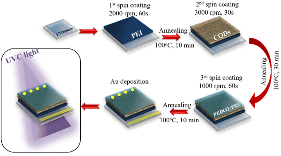 | ||
| Fig. 1 Schematic of fabrication of a UVC PD. | ||
2.4. Characterization and measurement
The morphological and crystallographic characteristics of the as-synthesized CQDs were analyzed using scanning electron microscopy (SEM; Hitachi SU8600, Tokyo, Japan) and X-ray diffraction (XRD; SmartLab, Rigaku, Tokyo, Japan). In addition, UV-vis spectrophotometry (LAMDA750, PerkinElmer, Waltham, USA) was used to investigate the optical properties and bandgaps of the CQDs. Fourier-transform infrared spectroscopy (FT-IR) (Thermo Fisher Scientific (iS50)) was used to examine the surface functional groups of the CQDs. The photoluminescence (PL; Fliorolog-QM, Horiba, Japan) of the CQDs was measured at an excitation wavelength of 260 nm. Cross-sectional SEM was used to measure the thickness and surface roughness of the CQD and PEI films. To evaluate the electrical characteristics of the fabricated PD, current–time (I–t) and current–voltage (I–V) profiles were recorded using a source meter (Keithley 2400, Tektronix, Beaverton, OR, USA) under UV irradiation at 254 and 365 nm (Spectroline UV-5NF, Spectronics Corporation, Melville, NY, USA). The potential was recorded using a potentiostat–galvanostat (Bio-Logic SP-240). A 254 nm UV lamp (Vilber Lourmat VL-6.LC) was used to illuminate the PD to measure the photo-response. Simulated solar irradiation was provided by a solar simulator (Polaromix K201, Solar simulator LAB 50, McScience K3000) with an irradiance of 100 mW cm−2. Electrical signals were recorded using a Keithley source meter (2400).3. Results and discussion
3.1. Characterization of photoactive materials
CQDs were prepared using a natural precursor (glucose) and a one-step ultrasonic reaction procedure, as shown in Fig. 2a. These CQDs served as a convenient and environmentally friendly platform for producing PD devices.77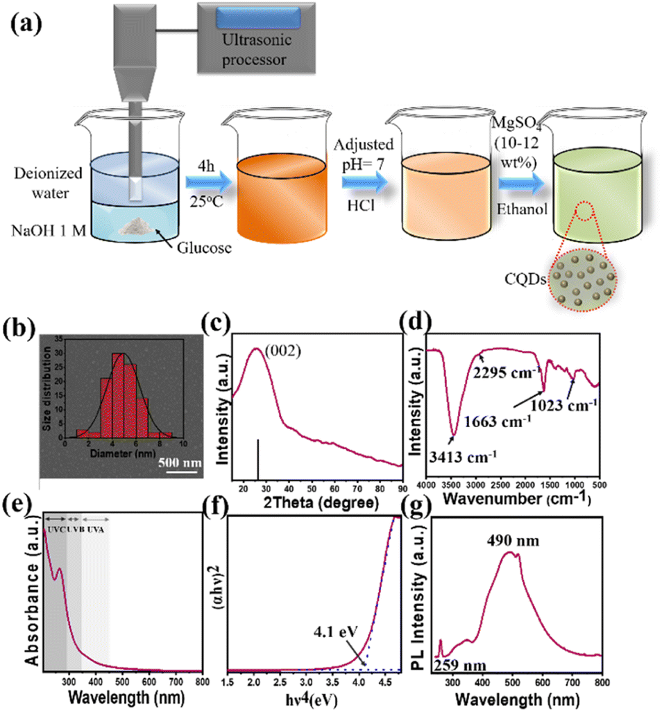 | ||
| Fig. 2 (a) Schematic of synthesis of CQDs, (b) SEM image of CQDs coated on glass (inset: size distribution of CQDs), (c) XRD pattern of CQDs, (d) FT-IR spectrum of CQDs, (e) UV-vis absorbance spectrum of CQDs, (f) Tauc plot of CQDs, and (g) PL spectrum (excitation wavelength of 260 nm) of CQDs. | ||
The emission properties and quality of the CQDs remained stable after storage in air for several months at ambient temperature, confirming their excellent optical stability. These CQDs could be easily dispersed in water without ultrasonication, facilitating their widespread application in PD devices.37 Furthermore, the advantages of CQDs, such as excellent optical properties, high response, and high chemical stability, will be demonstrated in this study. From the SEM image (Fig. 2b), the CQDs are aggregates of nanoparticles with a size of 2–9 nm, dominated by 5 nm particles. The peak at 25.9° in the XRD pattern, corresponding to the (002) plane, demonstrates the successful synthesis of the CQDs (Fig. 2c).78 Concurrently, FT-IR analyses were conducted to determine the surface functional groups on the CQDs. The distinctive O–H absorption band (3413 cm−1), C![[double bond, length as m-dash]](https://www.rsc.org/images/entities/char_e001.gif) O stretching vibration band (1651 cm−1), and C–O stretching vibration band (1023 cm−1) demonstrate the presence of the carboxylic group.79 Additionally, the weak signal at 2295 cm−1, attributed to –C
O stretching vibration band (1651 cm−1), and C–O stretching vibration band (1023 cm−1) demonstrate the presence of the carboxylic group.79 Additionally, the weak signal at 2295 cm−1, attributed to –C![[triple bond, length as m-dash]](https://www.rsc.org/images/entities/char_e002.gif) N, indicates the presence of amino-containing functional groups, which are required for streptavidin conjugation.80,81 The optical properties of the CQDs are displayed in Fig. 2e. The CQDs could absorb light in UVC range selectively, whereas the absorbance in the UVB range was minimal (visible blindness). Owing to the quantum confinement effect, the optical bandgap estimated from the Tauc plot is 4.1 eV (as shown in Fig. 2f), which is significantly greater than that of other carbon-based materials. Because of their large bandgap and selective absorption ability in UVC range, the prepared CQDs are excellent materials for UVC PDs. The transmittance of the CQDs in the UVC range was significantly low (∼4% at 254 nm; Fig. S1a†). Nevertheless, because CQDs are essential materials with high electron mobility, they cannot absorb light in the UVC region (Fig. S1b†). The functional groups on the surface of the CQDs formed an insulating shell, and the repulsive forces between the functional groups assisted in dispersing the CQDs, which retarded electrical transport, generated an inevitable leakage current, and reduced light absorption in the UVC region. Decreasing the concentration of CQDs can reduce the number of similarly charged particles (repulsive effect) and improve the charge transport pathway in the film, thus promoting the detection of UVC light. The CQD solutions were diluted to 60, 50, 40, 30, and 20 wt%, and the corresponding samples are denoted as CQDs-60, CQDs-50, CQDs-40, CQDs-30, and CQDs-20, respectively. The PL spectra (Fig. 2g) of the CQDs displayed two emission peaks at approximately 259 and 490 nm following excitation at 260 nm. The emission of the intermediate states of the CQDs resulting from surface defects, such as oxygen vacancies, is indicated by the peak at approximately 490 nm, whereas the peak at 259 nm represents the recombination of excitations and return to the ground state.
N, indicates the presence of amino-containing functional groups, which are required for streptavidin conjugation.80,81 The optical properties of the CQDs are displayed in Fig. 2e. The CQDs could absorb light in UVC range selectively, whereas the absorbance in the UVB range was minimal (visible blindness). Owing to the quantum confinement effect, the optical bandgap estimated from the Tauc plot is 4.1 eV (as shown in Fig. 2f), which is significantly greater than that of other carbon-based materials. Because of their large bandgap and selective absorption ability in UVC range, the prepared CQDs are excellent materials for UVC PDs. The transmittance of the CQDs in the UVC range was significantly low (∼4% at 254 nm; Fig. S1a†). Nevertheless, because CQDs are essential materials with high electron mobility, they cannot absorb light in the UVC region (Fig. S1b†). The functional groups on the surface of the CQDs formed an insulating shell, and the repulsive forces between the functional groups assisted in dispersing the CQDs, which retarded electrical transport, generated an inevitable leakage current, and reduced light absorption in the UVC region. Decreasing the concentration of CQDs can reduce the number of similarly charged particles (repulsive effect) and improve the charge transport pathway in the film, thus promoting the detection of UVC light. The CQD solutions were diluted to 60, 50, 40, 30, and 20 wt%, and the corresponding samples are denoted as CQDs-60, CQDs-50, CQDs-40, CQDs-30, and CQDs-20, respectively. The PL spectra (Fig. 2g) of the CQDs displayed two emission peaks at approximately 259 and 490 nm following excitation at 260 nm. The emission of the intermediate states of the CQDs resulting from surface defects, such as oxygen vacancies, is indicated by the peak at approximately 490 nm, whereas the peak at 259 nm represents the recombination of excitations and return to the ground state.
To understand the photoelectric conversion mechanism of the prepared PD, Fig. 3a shows the energy band diagrams of individual constituents of the device, including their conduction bands (CB) and valence bands (VB). FTO and Au were used as the bottom and top electrodes for the collection of electrons and holes, respectively.82–85 Here, a thin film of PEI is sandwiched between the CQD and FTO/glass substrate. The PEI interfacial layer supports close film formation and separates the top and bottom electrodes. The VB of the PEI layer was lower than that of the CQDs, which hindered hole transport from the CQD to the FTO. Furthermore, the CB of PEI is located between that of CQD and the Fermi level of FTO, facilitating electron extraction from CQD to FTO. The PD can operate without an external bias voltage owing to the difference in the Schottky barrier height between the PEI-coated FTO/CQD and PEDOT:PSS/CQD contacts. It is observed that the energy barriers at PEI-coated FTO/CQD and PEDOT:PSS/CQD interfaces are approximately 0.1 and 0.2 eV, respectively. Consequently, these energy barriers prevent charge carriers from migrating between electrodes, which is a main contributor to dark current. When the device is exposed to 254 nm UV illumination, electron–hole pairs are generated because the energy of the photons is greater than the bandgap of the CQD (as shown in Fig. 3b). The photoexcited electrons can overpass the lower Schottky barrier (0.1 eV) and be collected at the FTO side. For charge neutralization, the photogenerated holes concurrently move to the PEDOT:PSS side, generating a photocurrent at zero bias.
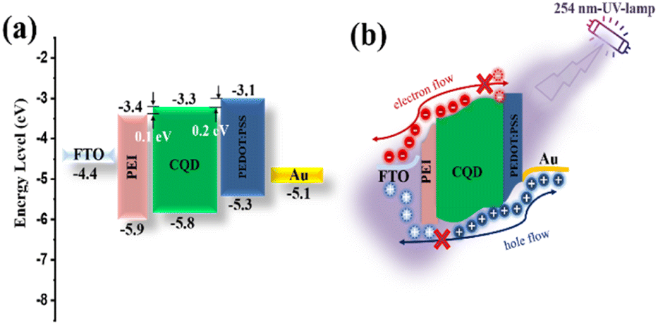 | ||
| Fig. 3 (a) Energy diagram of CQD-based PD device, and (b) operating mechanism of UVC detector under 254 nm illumination. | ||
3.2. Surface morphology of PEI and CQD films
The uniformity of the film significantly affects the performance of the PDs; for instance, an uneven surface can reduce energy loss by mitigating the scattering and reflection of incident light and improving trapping between the interfaces. Poor film uniformity also reduces the bonding between the interface layers, leading to a higher contact resistance. The morphologies of the spin-coated PEI (7 mg mL−1) and CQDs (CQDs-30) on the FTO/glass substrates are displayed in Fig. 4a and b. Both films were uniform, continuous, and devoid of any obvious cracks, flaws, or voids and could be confidently applied to create vertically stacked devices. The thickness of the film at different concentrations of PEI and CQD was investigated because this parameter significantly affects the ability of the device to absorb light (as shown in Fig. 4c, d, S2 and S3†). The PEI film was very thin (<100 nm in different solution concentrations), and its thickness was expected to positively affect light detection owing to a significant reduction in the number of trap positions and light penetration loss. An excessively thick CQD layer (>500 nm) increased the number of electron transport channels, creating favorable conditions for light penetration. Thus, a synergy between the PEI and CQD layers contributed to improving the device performance. Furthermore, the film thickness varied linearly with the concentration of both PEI and the CQDs. Increasing the PEI concentration from 1 to 9 mg mL−1 changed the film thickness from 51 to 86 nm (Fig. S2†). By contrast, when the concentration of the CQDs was decreased from 60 to 20 wt%, the film thickness gradually decreased from 782 to 701 nm because of the smaller number of CQDs in the ethanol solution (Fig. S3†). The thicknesses of the PEI and CQD films with respect to the solution concentration and weight percentage are shown in Fig. 4e and f. As the concentration of the solution increased, the thickness of the PEI film increased linearly (coefficient of determination (R2) = 0.9995). Moreover, in the case of the CQDs, decreasing the weight percentage of CQDs in the solution linearly reduced the film thickness (R2 = 0.9993). The high chemical stability of the CQDs was demonstrated via contact angle analysis (Fig. S4†). As the PEI concentration increased from 1 to 9 mg mL−1, the contact angle increased from 23.3° to 30.3°. Nevertheless, when the CQD concentration was varied from 60 to 20 wt%, the contact angle was stabilized at approximately 26°. The excellent chemical stability of the CQDs is favorable for large-scale applications.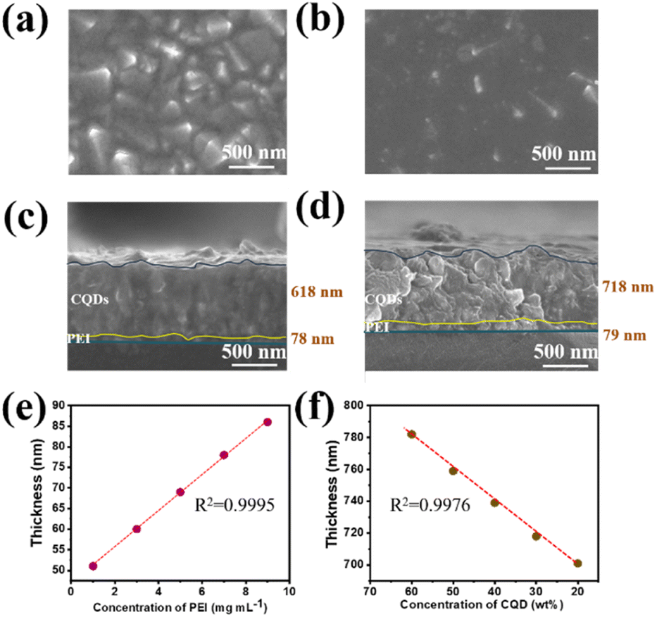 | ||
| Fig. 4 SEM image of (a) PEI layer (5 mg mL−1), (b) CQD layer (50 wt%). Cross-sectional SEM image of (c) PEI (5 mg mL−1), (d) CQDs (50 wt%). The film thickness changed as a function of the concentrations of (e) PEI and (f) CQDs in the solution. | ||
3.3. Effect of layer thickness on PD performance
We first investigated the influence of the PEI layer on the PD performance of the FTO/glass/CQDs/PEDO:TPSS/Au device. The responsivity (R) of the PD was calculated as follows:where P is the light intensity, A is the active area of the PD, and Idark and Iphoto are the currents under dark and illuminated conditions, respectively.
As shown in Fig. S5a and b,† the dark current level of the device with PEI was higher than that without PEI at zero bias. However, when illuminated at 254 nm, the photocurrent generated by the device with PEI was significantly higher (86 nA) than that without PEI (39 nA) (Fig. S5c†). Because of the decreased photocurrent, the device with PEI exhibited a higher responsivity than that without PEI. Fig. S6 and S7† show the I–V profiles of the PEI and CQD single-layer devices (FTO-glass/PEI/Au and FTO-glass/CQDs/Au). A linear I–V profile was detected, suggesting ohmic contacts were formed at the semiconductor/electrode interfaces because PEI had a higher Fermi level than both electrodes (FTO/glass and Au) (Fig. S6†). By contrast, the coexistence of ohmic (CQD/Au) and Schottky (CQD/FTO-glass) contacts caused nonlinear I–V behavior in the CQD single-layer device (Fig. S7†). Consequently, the absence of a PEI structure in the device with Schottky barriers restricts the flow of electrons from the semiconductor to the electrode and lowers the photocurrent (Fig. S5c†).
The number of charge carriers in heterojunction devices is significantly influenced by the thickness of the photoactive layer, which in turn affects the performance of the device. Fig. 5a, b and S8† present the photocurrent and responsivity of the device prepared by spin-coating as a function of the concentration of PEI and CQD (PEI: 1, 3, 5, 7, and 9 mg mL−1, and CQDs: 20, 30, 40, 50, and 60 wt%). Another essential metric for PDs is detectivity (D*), which indicates the minimum detectable light intensity from the device. D* is defined as follows:
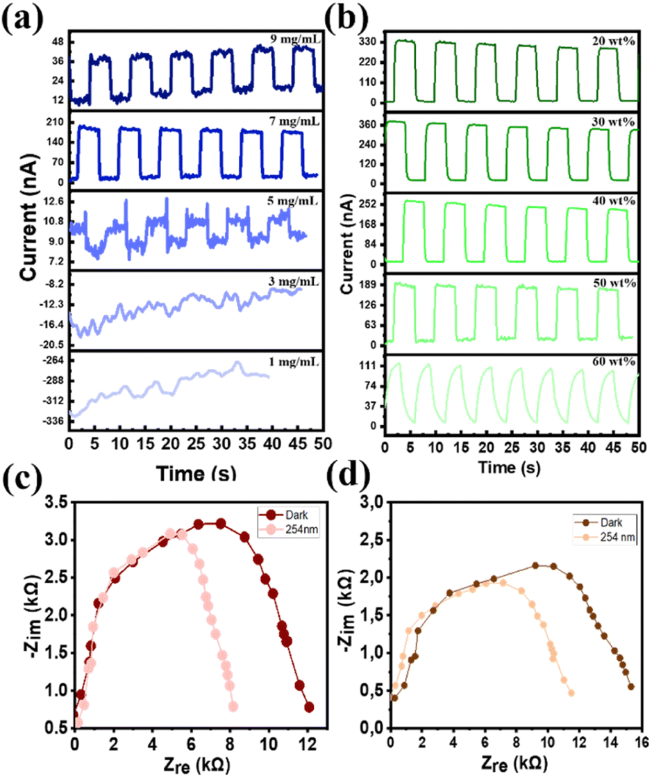 | ||
| Fig. 5 Photocurrent of (a) PEI at different solution concentrations, (b) CQDs at different concentrations. Nyquist plots of (c) PEI (solution concentration: 7 mg mL−1) and (d) CQDs (concentration: 30 wt%). | ||
In short, the photocurrent depends on the concentrations of PEI and CQD solution. More importantly, the photocurrent development mechanism is governed by the properties and thicknesses of the films in the PD device. PEI acts as a buffer layer, stabilizing the CQD and FTO electrode interface. Increasing the PEI thickness effectively controls the electrons trapped in the intrinsic vacancies and grain boundaries that can be instantly released from the PEI/CQD interface when the CQDs are exposed to radiation. However, a PEI film with excessive thickness can reduce the 254 nm light intensity in the absorption region. In contrast, CQDs act as a potential photoactive layer. A thinner CQD film shortens the travel distance of electrons, and fewer electrons are trapped in O vacancies and grain boundaries. However, excessive photocell reduction due to the excessively thin CQD layer will reduce the photocurrent in PEI films, deteriorating the PD performance. Therefore, adjusting the thickness of the PEI layer is necessary for optimizing the effective transport path in photovoltaic cells. Thus, the optimal conditions for the CQD and PEI layers were expected to produce a reasonably high photocurrent with a fast response. Under optimal conditions, the device can generate the highest on/off current ratio to achieve self-powered operation without consuming external energy.
Similar phenomena (brief spikes during pulsed light) have been documented for several optoelectronic devices, such as solar cells and PDs. Fig. 5c and d show the Nyquist plots of PEI and CQD films when the devices were illuminated by a light source with a wavelength of 254 nm at zero bias and in complete darkness. The PEI and CQD films were prepared from 7 mg mL−1 PEI and 30 wt% CQD solutions, respectively (Plots for each concentration are displayed individually in Fig. S11†). The radius of the semicircle in the Nyquist plot represents the charge-transfer resistance (Rct). With light illumination, the number of photocarriers increased in the absorbance zone, reducing the radius of the semicircle. Because the trap sites in the thicker films enhanced the recombination of the electrons and holes, the radii of the semicircles in Fig. S10† generally increased as the concentration of the solution increased. Specifically, light with a wavelength of 254 nm could not reach the absorbance zone when the thickness of the PEI layer was excessively high (PEI concentration 9 mg mL−1). Fewer electron–hole pairs are generated in the narrow absorbance zone of a thinner film (PEI-1 mg mL−1 and CQD-60 wt%); therefore, the Rct is low, and the reduction in Rct caused by light exposure was not noteworthy. On the contrary, the reduction in Rct due to light exposure was substantial for moderate film thicknesses (PEI-7 mg mL−1 and CQD-30 wt%), suggesting that a significant number of photocarriers was produced in the absorbance area. Consequently, impedance spectroscopy (IS) analysis validated that the optimal solution concentrations for PEI and CQD were 7 mg mL−1 and 30 wt%, respectively.
3.4. Performance of PEI–CQD heterojunction UVC PD
Fig. 6a schematically illustrates the vertical device structure, and Fig. 6b shows the cross-sectional SEM image of the optimized heterojunction PD (PEI-7/CQDs-30). The vertically stacked individual layers were clearly identified with well-defined thicknesses (Fig. 6b). In general, the boundaries of all organic materials are clearly shown. The thicknesses of the PEI, CQDs, PEDOT:PSS, and Au film layers were 76, 710, 130, and 80 nm, respectively. The I–t curves at different light intensities and bias voltages when exposed to 254 nm light are shown in Fig. 6c. Owing to the production of more photoelectrons at the PEI/CQD interface, the photocurrent increased from 160.8 to 190.8 nA at zero bias as the light intensity increased from 0.28 to 0.6 mW cm−2. Thus, the best-performed CQD-based PD device reaches a photocurrent of 190 nA, responsivity of 1.5 mA W−1, and detectivity of 1.8 × 10¹⁰ Jones under 0.6 mW cm−2 (as shown in Fig. 6c and S12†). Regardless of the bias voltage, a steady drop in the responsivity was also observed as the light intensity increased from 0.6 to 0.8 mW cm−2. This is explained by the non-linear increase in the on/off ratio with an increase in the light intensity. The optical-band selectivity of the PD was determined by evaluating its spectral responsivity. Similar trends were observed under different bias settings (Fig. S13†). By contrast, a higher bias voltage resulted in a notably higher dark current and a lower on/off ratio. Notably, for bias voltages of 0, 5, and 10 mV, the dark currents were 19.86, 114.1, and 218.9 nA, respectively. The movement of charge carriers trapped in the defects of the CQD layer, and the increased drift speed caused a large dark current under bias conditions. The spectral responsiveness in the 220–800 nm wavelength range is displayed in Fig. 6d. The D* exhibited a similar trend to that of responsivity, as evidenced by its negative correlation with both bias voltage and light intensity (Fig. 6e).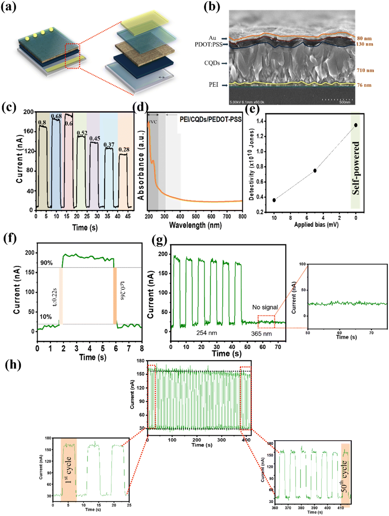 | ||
| Fig. 6 (a) Schematic of UVC PD structure, (b) cross-sectional SEM image of the optimized PD, (c) photocurrent under different light intensities at zero bias, (d) spectral responsivity of the self-powered device, (e) detectivity of PD under different applied bias, (f) rise and decay times of the PD, (g) photocurrent versus time for PD under UVC and UVA illumination with an intensity of 0.6 mW cm−2, and (h) long-term performance (50 cycles) when the PD was subjected to repeated on/off cycles (4 s of illumination per cycle). | ||
Because of the low dark current density, high detectivity of 1.3 × 10¹⁰ Jones was observed at zero bias. Consequently, the self-powered operation could improve detectivity and responsivity. The rise (time required for the maximum current to increase from 10% to 90%) or decay (time required for maximum current to decrease from 90% to 10%) period is referred to as the response time (Rt). The heterojunction PD exposed to 4 s light pulses had rise and decay times of 0.22 and 0.26 s, respectively, as shown in Fig. 6f. The CQD-based PD demonstrated high efficiency under irradiation at 254 nm compared with that under UV B-band (UVB) and UV A-band (UVA) light (no signal) (Fig. 6g and S14†). The applicability of PD sensors largely depends on the stability and continuity of the PDs. The photocurrent remained almost constant for 50 on/off light cycles, as illustrated in Fig. 6h (4 s of illumination for each pulse), indicating the consistent and reliable performance of the PD over an extended period of use.
Table 2 summarizes the performance of contemporary UV PDs. Compared with the performance of other recently reported UV PDs, the PD reported in this study exhibited high responsivity (1.5 mA W−1) and detectivity (1.8 × 10¹⁰ Jones) at 254 nm during self-powered operation. In comparison to the performance of other recent photoactive materials, our PEI–CQD exhibits high responsibility, many times higher than reported organic-based UV devices, along with self-powering ability as another advantage in this research. In summary, this work proposes a combined strategy to optimize PEI thickness for stabilizing the PEI/CQD interface and to use organic materials that have inherently high electronic conductivity with appropriate film thickness for enhancing PD performance. The optimal PEI thickness achieves stable electron mobility across the PEI/CQD interface (3.3 × 10⁻⁶ cm2 V−1 s−1). CQD films improve the photocurrent and responsibility to 360 nA and 1.5 mA W−1, respectively. Therefore, this discovery demonstrated a simple and effective process to achieve high-performance electrodes for optoelectronics, especially deep UV photodetectors.
| Photo-absorbing materials | Voltage (V) | Wavelength (nm) | Responsivity (mA W−1) | Detectivity (Jones) | Thickness (nm) | Ref. |
|---|---|---|---|---|---|---|
| a PC61BM – [6,6]-phenyl-C61-butyric acid methyl; Cy7-T:C60 – heptamethine cyanine dyes/C60 fullerene; 1(Pyrl):C60 – merocyanine/C60; polyTPD:SBDTIC – poly(N,N′-bis-4-butylphenyl-N,N′-bisphenyl)benzidine:(4,4,10,10-tetrakis(4-hexylphenyl)-5,11-(n-hexylthio)-4,10-dihydrodithienyl[1,2-b:4,5-b]benzodi-thiophene-2,8-diyl)bis(2-(3-oxo-2,3-dihydroinden-1-ylidene)malononitrile); PCZ-Th-DPP – phenanthrocarbazole:diketopyrrolopyrrole; M1:C60 – M-molecules and C60; CiInPc:C60 – indium(III) phthalocyanine chloride:C60; 1a:C60 – dipolar donor–acceptor (1a) molecules:C60; SubPc:C60 – boron subphthalocyanine chloride:C60; DMQA:SubPc – N,N-dimethyl quinacridone:SubPC; DM-2,9-DMQA:SubPc – 2,9-dimethylquinacridone (2,9-DMQA):SubPC; PCPDTBT:ZnO – poly[2,6-(4,4-bis-(2-ethylhexyl)-4H-cyclopenta [2,1-b; 3,4-b′]dithiophene)-alt-4,7(2,1,3-benzothiadiazole):ZnO; PSBOTz:PNDBO – (4,8-bis(5-((2-ethylhexyl)thio)thiophen-2-yl)benzo[1,2-b:4,5-b′]dithiophene-2,6-diyl-alt-2,5-bis(5-bromo-4-octylthiazol-2-yl)thiophene-2,5-diyl):N,N′-bis(2-ethylhexyl)-1,8:4,5-aphthalenetetracarboxdiimide-2,6-diyl-alt-1,8-octyldioxy-4,4-diphenyl; 1(Pyrl):1(Hex):C60 – 2-[4-(tert-butyl)thiazol-2(3H)-ylidene]malononitrile:2-aminothiophene:C60. | ||||||
| PC61BM | −1.0 | 500 | 0.03 | — | 86 | |
| PC61BM | −1.0 | 525 | 0.06 | 1.00 × 10¹¹ | 120 | 87 |
| Cy7-T:C60 | −1.0 | 850 | 0.12 | 1.00 × 10¹² | 30 | 88 |
| 1(Pyrl):C60 | 0 | 481 | 0.07 | 2.00 × 10¹¹ | 76 | 89 |
| PolyTPD:SBDTIC | 0 | 740 | 0.06 | 1.42 × 10¹³ | 70 | 40 |
| PCZ-Th-DPP | −1.0 | 709 | — | 4.63 × 10¹² | 300 | 90 |
| Rubrene:C60 | −1.0 | 470 | 0.21 | — | 70 | 91 |
| M1:C60 | −3.0 | 550 | 0.26 | 3.73 × 10¹³ | 85 | 92 |
| CiInPc:C60 | −1.0 | 705 | 0.45 | 3.30 × 10¹² | 120 | 93 |
| 1a:C60 | −3.0 | 560 | 0.32 | 4.37 × 10¹³ | 85 | 94 |
| SubPc:C60 | −1.0 | 600 | 0.08 | 7.50 × 10¹¹ | — | 95 |
| DMQA:SubPc | −5.0 | 586 | 0.27 | 2.34 × 10¹² | 90 | 96 |
| DM-2,9-DMQA:SubPc | −3.0 | 580 | 0.56 | 2.03 × 10¹² | 70 | 97 |
| PCPDTBT:ZnO | — | 725 | 0.40 | — | 70 | 98 |
| PSBOTz:PNDBO | −2.0 | 530 | 0.07 | 1.10 × 10¹³ | — | 99 |
| 1(Pyrl):1(Hex):C60 | 0 | 754 | 0.086 | 1.10 × 10¹⁰ | 40 | 100 |
| CQDs | 0 | 254 | 1.5 | 1.8 × 10¹⁰ | ∼700 | This study |
4. Conclusion
An all-organic-based, high-performance, self-powered PEI–CQD heterojunction UVC PD was developed through a simple, low-temperature solution process using natural precursors and a one-step ultrasonic reaction procedure. The CQDs were characterized by SEM, UV-vis absorbance spectroscopy, XRD, and FT-IR spectroscopy. The layer thicknesses of the PEI film and CQD film were optimized to achieve the best device performance. Under the optimal conditions, the PEI/CQD PD exhibits a strong photocurrent (1.5 mA W−1 at 254 nm), high detectability (1.8 × 10¹⁰ Jones at 254 nm), an ultrafast response speed, and long-term stability during the power supply sequence. Overall, the PEI/CQD PD reported in this study paves the way for the development of highly efficient, inexpensive, and form-factor UVC sensing devices for various applications.Data availability
The authors do not have permission to share data.Author contributions
Vo Pham Hoang Huy: data curation, writing – original draft, investigation. Chung Wung Bark: conceptualization, methodology, writing – review & editing, supervision, funding acquisition.Conflicts of interest
The authors declare that they have no known competing financial interests or personal relationships that could have appeared to influence the work reported in this paper.Acknowledgements
This work was supported by grants from the National Research Foundation of Korea (NRF) funded by the Ministry of Science and ICT (NRF-2020R1F1A1076576) and by the Korea Basic Science Institute grant funded by the Ministry of Education (2019R1A6C1010016). This work was supported by the Korea Institute of Energy Technology Evaluation and Planning (KETEP) and the Ministry of Trade, Industry, and Energy (MOTIE) of the Republic of Korea (no. 1415188041).Notes and references
- M. Razeghi, Short-wavelength solar-blind detectors-status, prospects, and markets, Proc. IEEE, 2002, 90(6), 1006–1014 CrossRef CAS.
- L. Sang, M. Liao and M. Sumiya, A Comprehensive Review of Semiconductor Ultraviolet Photodetectors: From Thin Film to One-Dimensional Nanostructures, Sensors, 2013, 13, 10482–10518, DOI:10.3390/s130810482.
- P. Autier, et al., Exposure to Artificial UV Radiation and Skin Cancer, Lyon, France, 2005, p. 2005 Search PubMed.
- S. Li, et al., UV-C irradiation for harmful algal blooms control: A literature review on effectiveness, mechanisms, influencing factors and facilities, Sci. Total Environ., 2020, 723, 137986 CrossRef CAS PubMed.
- T. Dai, et al., Ultraviolet C irradiation: an alternative antimicrobial approach to localized infections, Expert Rev. Anti-Infect. Ther., 2012, 10(2), 185–195 CrossRef CAS PubMed.
- T. Phukan, A. N. Rai and M. B. Syiem, Dose dependent variance in UV-C radiation induced effects on carbon and nitrogen metabolism in the cyanobacterium Nostoc muscorum Meg1, Ecotoxicol. Environ. Saf., 2018, 155, 171–179 CrossRef CAS PubMed.
- A. Trevisan, et al., Unusual High Exposure to Ultraviolet-C Radiation, Photochem. Photobiol., 2006, 82(4), 1077–1079 CrossRef CAS PubMed.
- M. Bruze, M. Hindsén and L. Trulsson, Dermatitis with an unusual explanation in a welder, Acta Derm.-Venereol., 1994, 74(5), 380–382 CrossRef CAS PubMed.
- A. Forsyth, C. W. Ide and H. Moseley, Acute sunburn due to accidental irradiation with UVC, Contact Dermatitis, 1991, 24(2), 141–142 CrossRef CAS PubMed.
- X. Li, et al., Background limited ultraviolet photodetectors of solar-blind ultraviolet detection, Appl. Phys. Lett., 2013, 103(17), 171110 CrossRef.
- D. Kaur and M. Kumar, A Strategic Review on Gallium Oxide Based Deep-Ultraviolet Photodetectors: Recent Progress and Future Prospects, Adv. Opt. Mater., 2021, 9(9), 2002160 CrossRef CAS.
- S. Kim, et al., Alpha-phase gallium oxide-based UVC photodetector with high sensitivity and visible blindness, APL Mater., 2023, 11(6), 061107 CrossRef CAS.
- B. Zhao, et al., An Ultrahigh Responsivity (9.7 mA W−1) Self-Powered Solar-Blind Photodetector Based on Individual ZnO–Ga2O3 Heterostructures, Adv. Funct. Mater., 2017, 27(17), 1700264 CrossRef.
- S. Oh, C.-K. Kim and J. Kim, High Responsivity β-Ga2O3 Metal–Semiconductor–Metal Solar-Blind Photodetectors with Ultraviolet Transparent Graphene Electrodes, ACS Photonics, 2018, 5(3), 1123–1128 CrossRef CAS.
- K. Arora, et al., Ultrahigh Performance of Self-Powered β-Ga2O3 Thin Film Solar-Blind Photodetector Grown on Cost-Effective Si Substrate Using High-Temperature Seed Layer, ACS Photonics, 2018, 5(6), 2391–2401 CrossRef CAS.
- C. Lin, et al., npj 2D Mater. Appl., 2018, 2, 23 CrossRef.
- T. C. Wei, et al., See-Through Ga2O3 Solar-Blind Photodetectors for Use in Harsh Environments, IEEE J. Sel. Top. Quantum Electron., 2014, 20(6), 112–117 Search PubMed.
- H. Kan, et al., Ultrafast Photovoltaic-Type Deep Ultraviolet Photodetectors Using Hybrid Zero-/Two-Dimensional Heterojunctions, ACS Appl. Mater. Interfaces, 2019, 11(8), 8412–8418 CrossRef CAS PubMed.
- E. Park, et al., Self-powered high-performance ultraviolet C photodetector based on poly(9-vinyl carbazole)/SnO2 quantum dot heterojunction, J. Alloys Compd., 2022, 918, 165502 CrossRef CAS.
- J. D. Myers and J. Xue, Organic Semiconductors and their Applications in Photovoltaic Devices, Polym. Rev., 2012, 52(1), 1–37 CrossRef CAS.
- M. J. Griffith, et al., Combining Printing, Coating, and Vacuum Deposition on the Roll-to-Roll Scale: A Hybrid Organic Photovoltaics Fabrication, IEEE J. Sel. Top. Quantum Electron., 2016, 22(1), 112–125 Search PubMed.
- T. R. Andersen, et al., Comparison of inorganic electron transport layers in fully roll-to-roll coated/printed organic photovoltaics in normal geometry, J. Mater. Chem. A, 2016, 4(41), 15986–15996 RSC.
- M. J. Griffith, et al., Controlling Nanostructure in Inkjet Printed Organic Transistors for Pressure Sensing Applications, Nanomaterials, 2021, 11(5), 1185 CrossRef CAS PubMed.
- J. A. Posar, et al., Polymer Photodetectors for Printable, Flexible, and Fully Tissue Equivalent X-Ray Detection with Zero-Bias Operation and Ultrafast Temporal Responses, Adv. Mater. Technol., 2021, 6(9), 2001298 CrossRef CAS.
- H. Klauk, Organic thin-film transistors, Chem. Soc. Rev., 2010, 39(7), 2643–2666 RSC.
- G. C. Welch and M. Leclerc, Organic Solar Cells – Special Issue, Chem. Rec., 2019, 19(6), 961 CrossRef CAS PubMed.
- M. Marks, et al., Building intermixed donor–acceptor architectures for water-processable organic photovoltaics, Phys. Chem. Chem. Phys., 2019, 21(10), 5705–5715 RSC.
- M. Ameri, et al., Role of Stabilizing Surfactants on Capacitance, Charge, and Ion Transport in Organic Nanoparticle-Based Electronic Devices, ACS Appl. Mater. Interfaces, 2019, 11(10), 10074–10088 CrossRef CAS PubMed.
- W. Huang, et al., Wearable Organic Nano-sensors, in Flexible and Wearable Electronics for Smart Clothing, 2020, pp. 1–27 Search PubMed.
- H.-W. Chen, et al., Liquid crystal display and organic light-emitting diode display: present status and future perspectives, Light: Sci. Appl., 2018, 7(3), 17168 CrossRef CAS PubMed.
- P. C. Y. Chow and T. Someya, Organic Photodetectors for Next-Generation Wearable Electronics, Adv. Mater., 2020, 32(15), 1902045 CrossRef CAS PubMed.
- Z. Zhang, et al., Ultraviolet Photodetectors Based on Polymer Microwire Arrays toward Wearable Medical Devices, ACS Appl. Mater. Interfaces, 2022, 14(36), 41257–41263 CrossRef CAS PubMed.
- X. Zhou, et al., High—Performance Solar-Blind Deep Ultraviolet Photodetector Based on Individual Single-Crystalline Zn2GeO4 Nanowire, Adv. Funct. Mater., 2016, 26(5), 704–712 CrossRef CAS.
- H. Chen, et al., Nanostructured Photodetectors: From Ultraviolet to Terahertz, Adv. Mater., 2016, 28(3), 403–433 CrossRef CAS PubMed.
- V.-T. Tran, et al., All-inkjet-printed flexible ZnO micro photodetector for a wearable UV monitoring device, Nanotechnology, 2017, 28(9), 095204 CrossRef PubMed.
- D. Shao, et al., An ultraviolet photodetector fabricated from WO3 nanodiscs/reduced graphene oxide composite material, Nanotechnology, 2013, 24(29), 295701 CrossRef PubMed.
- S. Nakagomi, et al., Deep ultraviolet photodiodes based on the β-Ga2O3/GaN heterojunction, Sens. Actuators, A, 2015, 232, 208–213 CrossRef CAS.
- S. Y. Heo, et al., Wireless, battery-free, flexible, miniaturized dosimeters monitor exposure to solar radiation and to light for phototherapy, Sci. Transl. Med., 2018, 10(470), eaau1643 CrossRef CAS PubMed.
- K. Vasseur, et al., Structural Evolution of Evaporated Lead Phthalocyanine Thin Films for Near-Infrared Sensitive Solar Cells, Chem. Mater., 2011, 23(3), 886–895 CrossRef CAS.
- K. Xia, et al., Narrowband-Absorption-Type Organic Photodetectors for the Far-Red Range Based on Fullerene-Free Bulk Heterojunctions, Adv. Opt. Mater., 2020, 8(8), 1902056 CrossRef CAS.
- M. A. Alam, et al., The essence and efficiency limits of bulk-heterostructure organic solar cells: A polymer-to-panel perspective, J. Mater. Res., 2013, 28(4), 541–557 CrossRef CAS.
- Q. Liu, S. E. Bottle and P. Sonar, Developments of Diketopyrrolopyrrole-Dye-Based Organic Semiconductors for a Wide Range of Applications in Electronics, Adv. Mater., 2020, 32(4), 1903882 CrossRef CAS PubMed.
- H. W. Lin, et al., Highly Efficient Visible-Blind Organic Ultraviolet Photodetectors, Adv. Mater., 2005, 17(20), 2489–2493 CrossRef CAS.
- S. Dhara and P. K. Giri, Stable p-type conductivity and enhanced photoconductivity from nitrogen-doped annealed ZnO thin film, Thin Solid Films, 2012, 520(15), 5000–5006 CrossRef CAS.
- R. Parize, et al., Effects of Polyethylenimine and Its Molecular Weight on the Chemical Bath Deposition of ZnO Nanowires, ACS Omega, 2018, 3(10), 12457–12464 CrossRef CAS PubMed.
- J. Qiu, et al., Solution-derived 40 μm vertically aligned ZnO nanowire arrays as photoelectrodes in dye-sensitized solar cells, Nanotechnology, 2010, 21(19), 195602 CrossRef PubMed.
- C. P. Burke-Govey and N. O. V. Plank, The influence of polyethylenimine molecular weight on hydrothermally-synthesised ZnO nanowire morphology, Int. J. Nanotechnol., 2017, 14(1–6), 47–55 CrossRef CAS.
- M. Chen, et al., X-ray photoelectron spectroscopy and auger electron spectroscopy studies of Al-doped ZnO films, Appl. Surf. Sci., 2000, 158(1), 134–140 CrossRef CAS.
- Y. Zhou, et al., A Universal Method to Produce Low-Work Function Electrodes for Organic Electronics, Science, 2012, 336(6079), 327–332 CrossRef CAS PubMed.
- M. Cesarini, et al., Reproducible, High Performance Fully Printed Photodiodes on Flexible Substrates through the Use of a Polyethylenimine Interlayer, ACS Appl. Mater. Interfaces, 2018, 10(38), 32380–32386 CrossRef CAS PubMed.
- F. Yuan, et al., Bright Multicolor Bandgap Fluorescent Carbon Quantum Dots for Electroluminescent Light-Emitting Diodes, Adv. Mater., 2017, 29(3), 1604436 CrossRef PubMed.
- Y. Dong, et al., Polyamine-functionalized carbon quantum dots for chemical sensing, Carbon, 2012, 50(8), 2810–2815 CrossRef CAS.
- K. A. S. Fernando, et al., Carbon Quantum Dots and Applications in Photocatalytic Energy Conversion, ACS Appl. Mater. Interfaces, 2015, 7(16), 8363–8376 CrossRef CAS PubMed.
- Y.-Q. Zhang, et al., N-doped carbon quantum dots for TiO2-based photocatalysts and dye-sensitized solar cells, Nano Energy, 2013, 2(5), 545–552 CrossRef CAS.
- X. Yu, et al., Preparation and visible light photocatalytic activity of carbon quantum dots/TiO2 nanosheet composites, Carbon, 2014, 68, 718–724 CrossRef CAS.
- Y.-L. Zhang, et al., Graphitic carbon quantum dots as a fluorescent sensing platform for highly efficient detection of Fe3+ ions, RSC Adv., 2013, 3(11), 3733–3738 RSC.
- Y. Dong, et al., Polyamine-Functionalized Carbon Quantum Dots as Fluorescent Probes for Selective and Sensitive Detection of Copper Ions, Anal. Chem., 2012, 84(14), 6220–6224 CrossRef CAS PubMed.
- P. Mirtchev, et al., Solution phase synthesis of carbon quantum dots as sensitizers for nanocrystalline TiO2 solar cells, J. Mater. Chem., 2012, 22(4), 1265–1269 RSC.
- H. Li, et al., Carbon Quantum Dots/TiOx Electron Transport Layer Boosts Efficiency of Planar Heterojunction Perovskite Solar Cells to 19%, Nano Lett., 2017, 17(4), 2328–2335 CrossRef CAS PubMed.
- A. H. Loo, et al., Carboxylic Carbon Quantum Dots as a Fluorescent Sensing Platform for DNA Detection, ACS Appl. Mater. Interfaces, 2016, 8(3), 1951–1957 CrossRef CAS PubMed.
- S.-W. Lee, et al., Low dark current and improved detectivity of hybrid ultraviolet photodetector based on carbon-quantum-dots/zinc-oxide-nanorod composites, Org. Electron., 2016, 39, 250–257 CrossRef CAS.
- K. Li, et al., Built-in electric field promotes photoexcitation separation and depletion of most carriers in TiO2:C UV detectors, Nanotechnology, 2019, 30(29), 295502 CrossRef CAS PubMed.
- P. Sahatiya, S. S. Jones and S. Badhulika, 2D MoS2–carbon quantum dot hybrid based large area, flexible UV-vis-NIR photodetector on paper substrate, Appl. Mater. Today, 2018, 10, 106–114 CrossRef.
- W. Zhang, et al., High-performance AlGaN metal–semiconductor–metal solar-blind ultraviolet photodetectors by localized surface plasmon enhancement, Appl. Phys. Lett., 2015, 106(2), 021112 CrossRef.
- E. A. Azhar, et al., Vapor-Transport Synthesis and Annealing Study of ZnxMg1−xO Nanowire Arrays for Selective, Solar-Blind UV-C Detection, ACS Omega, 2018, 3(5), 4899–4907 CrossRef CAS PubMed.
- J. Ahn, et al., Ultrahigh Deep-Ultraviolet Responsivity of a β-Ga2O3/MgO Heterostructure-Based Phototransistor, ACS Photonics, 2021, 8(2), 557–566 CrossRef CAS.
- S.-H. Tsai, et al., Deep-Ultraviolet Photodetectors Based on Epitaxial ZnGa2O4 Thin Films, Sci. Rep., 2018, 8(1), 14056 CrossRef PubMed.
- H. Liu, et al., High-performance deep ultraviolet photodetectors based on few-layer hexagonal boron nitride, Nanoscale, 2018, 10(12), 5559–5565 RSC.
- J. Xing, et al., Solar-blind deep-ultraviolet photodetectors based on an LaAlO3 single crystal, Opt. Lett., 2009, 34(11), 1675–1677 CrossRef CAS PubMed.
- L. Li, et al., Ultrahigh-Performance Solar-Blind Photodetectors Based on Individual Single-crystalline In2Ge2O7 Nanobelts, Adv. Mater., 2010, 22(45), 5145–5149 CrossRef CAS PubMed.
- B. Yu, et al., Facile hydrothermal synthesis of SnO2 quantum dots with enhanced photocatalytic degradation activity: Role of surface modification with chloroacetic acid, J. Environ. Chem. Eng., 2021, 9(4), 105618 CrossRef CAS.
- T. Zou, et al., Enhanced UV-C Detection of Perovskite Photodetector Arrays via Inorganic CsPbBr3 Quantum Dot Down-Conversion Layer, Adv. Opt. Mater., 2019, 7(11), 1801812 CrossRef.
- W. J. Kuang, et al., Solution-Processed Solar-Blind Ultraviolet Photodetectors Based on ZnS Quantum Dots, IEEE Photonics Technol. Lett., 2018, 30(15), 1384–1387 CAS.
- Y. Xia, et al., Solution-processed solar-blind deep ultraviolet photodetectors based on strongly quantum confined ZnS quantum dots, J. Mater. Chem. C, 2018, 6(42), 11266–11271 RSC.
- Z. Long, et al., Cross-Bar SnO2-NiO Nanofiber-Array-Based Transparent Photodetectors with High Detectivity, Adv. Electron. Mater., 2020, 6(1), 1901048 CrossRef CAS.
- H. Alamoudi, et al., Enhanced solar-blind deep UV photodetectors based on solution-processed p-MnO quantum dots and n-GaN p–n junction-structure, Appl. Phys. Lett., 2022, 120(12), 122102 CrossRef CAS.
- H. Li, et al., One-step ultrasonic synthesis of water-soluble carbon nanoparticles with excellent photoluminescent properties, Carbon, 2011, 49(2), 605–609 CrossRef CAS.
- J. Zheng, et al., An Efficient Synthesis and Photoelectric Properties of Green Carbon Quantum Dots with High Fluorescent Quantum Yield, Nanomaterials, 2020, 10(1), 82 CrossRef CAS PubMed.
- C. Zhu, J. Zhai and S. Dong, Bifunctional fluorescent carbon nanodots: green synthesis via soy milk and application as metal-free electrocatalysts for oxygen reduction, Chem. Commun., 2012, 48(75), 9367–9369 RSC.
- P. C. Hsu and H. T. Chang, Synthesis of high-quality carbon nanodots from hydrophilic compounds: role of functional groups, Chem. Commun., 2012, 48(33), 3984–3986 RSC.
- Q. Liang, et al., Easy synthesis of highly fluorescent carbon quantum dots from gelatin and their luminescent properties and applications, Carbon, 2013, 60, 421–428 CrossRef CAS.
- T. M. H. Nguyen and C. W. Bark, Self-Powered UVC Photodetector Based on Europium Metal–Organic Framework for Facile Monitoring Invisible Fire, ACS Appl. Mater. Interfaces, 2022, 14(40), 45573–45581 CrossRef CAS PubMed.
- N. A. Issa, et al., Photovoltaic performance improvement of organic solar cell with ZnO nanorod arrays as electron transport layer using carbon quantum dots-incorporated photoactive layer, Opt. Mater., 2022, 132, 112876 CrossRef CAS.
- M. H. Tran, T. M. H. Nguyen and C. W. Bark, Toward Industrial Production of a High-Performance Self-Powered Ultraviolet Photodetector Using Nanoporous Al-Doped ZnO Thin Films, ACS Omega, 2023, 8(38), 35343–35350 CrossRef CAS PubMed.
- A. J. Olivares, et al., Nanostructural Modification of PEDOT:PSS for High Charge Carrier Collection in Hybrid Frontal Interface of Solar Cells, Polymers, 2019, 11(6), 1034 CrossRef CAS PubMed.
- R. D. Jansen-van Vuuren, et al., Colour selective organic photodetectors utilizing ketocyanine-cored dendrimers, J. Mater. Chem. C, 2013, 1(22), 3532–3543 RSC.
- D. M. Lyons, et al., Narrow band green organic photodiodes for imaging, Org. Electron., 2014, 15(11), 2903–2911 CrossRef CAS.
- H. Zhang, et al., Transparent Organic Photodetector using a Near-Infrared Absorbing Cyanine Dye, Sci. Rep., 2015, 5(1), 9439 CrossRef CAS PubMed.
- A. Liess, et al., Ultranarrow Bandwidth Organic Photodiodes by Exchange Narrowing in Merocyanine H- and J-Aggregate Excitonic Systems, Adv. Funct. Mater., 2019, 29(21), 1805058 CrossRef.
- S. Z. Hassan, et al., Molecular Engineering of a Donor–Acceptor Polymer To Realize Single Band Absorption toward a Red-Selective Thin-Film Organic Photodiode, ACS Appl. Mater. Interfaces, 2019, 11(31), 28106–28114 CrossRef CAS PubMed.
- W. Li, et al., Squarylium and rubrene based filterless narrowband photodetectors for an all-organic two-channel visible light communication system, Org. Electron., 2016, 37, 346–351 CrossRef CAS.
- M. G. Han, et al., Narrow-Band Organic Photodiodes for High-Resolution Imaging, ACS Appl. Mater. Interfaces, 2016, 8(39), 26143–26151 CrossRef CAS PubMed.
- C. W. Joo, et al., High-performance fab-compatible processed near-infrared organic thin-film photodiode with 3.3×10¹² Jones detectivity and 80% external quantum efficiency, Org. Electron., 2019, 70, 101–106 CrossRef CAS.
- G. H. Lee, et al., Green-light-selective organic photodiodes for full-color imaging, Opt. Express, 2019, 27(18), 25410–25419 CrossRef CAS PubMed.
- D. Shen, et al., Trilayer organic narrowband photodetector with electrically-switchable spectral range and color sensing ability, J. Mater. Chem. C, 2021, 9(11), 3814–3819 RSC.
- K.-H. Lee, et al., Green-Sensitive Organic Photodetectors with High Sensitivity and Spectral Selectivity Using Subphthalocyanine Derivatives, ACS Appl. Mater. Interfaces, 2013, 5(24), 13089–13095 CrossRef CAS PubMed.
- S.-J. Lim, et al., Organic-on-silicon complementary metal–oxide–semiconductor colour image sensors, Sci. Rep., 2015, 5(1), 7708 CrossRef CAS PubMed.
- J. Y. Kim, et al., Versatile use of ZnO interlayer in hybrid solar cells for self-powered near infra-red photo-detecting application, J. Alloys Compd., 2020, 813, 152202 CrossRef CAS.
- J. Kang, et al., High-Detectivity Green-Selective All-Polymer p–n Junction Photodetectors, Adv. Opt. Mater., 2020, 8(23), 2001038 CrossRef CAS.
- T. Schembri, et al., Semitransparent Layers of Social Self-Sorting Merocyanine Dyes for Ultranarrow Bandwidth Organic Photodiodes, Adv. Opt. Mater., 2021, 9(15), 2100213 CrossRef CAS.
Footnote |
| † Electronic supplementary information (ESI) available. See DOI: https://doi.org/10.1039/d3ra08538d |
| This journal is © The Royal Society of Chemistry 2024 |