
 Open Access Article
 This Open Access Article is licensed under a Creative Commons Attribution-Non Commercial 3.0 Unported Licence
An amorphous MgF2 anti-reflective thin film for enhanced performance of inverted organic–inorganic perovskite solar cells†
Wenhui Lia,
Wenhuan Caoa,
Huawei Zhou *a,
Xianxi Zhang*a and
Kai Wang*b
*a,
Xianxi Zhang*a and
Kai Wang*b
aSchool of Chemistry and Chemical Engineering, College of Materials Science and Engineering, Shandong Provincial Key Laboratory/Collaborative Innovation Center of Chemical Energy Storage, Liaocheng University, China. E-mail: zhouhuaweiopv@163.com; xxzhang3@126.com
bDalian National Laboratory for Clean Energy, iChEM, Dalian Institute of Chemical Physics, Chinese Academy of Sciences, Dalian 116023, Liaoning, China. E-mail: wangkai@dicp.ac.cn
First published on 16th January 2024
Abstract
The effective control of light plays an important role in optoelectronic devices. However, the effect of anti-reflection thin film (ARTF) in inverted perovskite solar cells (PSCs) (p-i-n) has so far remained elusive. Herein, MgF2 ARTF with different thicknesses (approximately 100, 330, and 560 nm) were deposited on the glass side of FTO conductive glass substrates by vacuum thermal evaporation. The results of reflectance and transmittance spectroscopy show that approximately 330 nm MgF2 ARTF can reduce reflectivity and increase transmittance on FTO conductive glass substrates. The results of SEM, XRD, and AFM show that the surface of amorphous MgF2 ARTF possesses a lot of nanoscale pits. The effect of the MgF2 ARTF on the performance of inverted perovskite solar cells (PSCs) (p-i-n) was investigated. The power conversion efficiencies (PCE) of inverted PSCs without and with MgF2 ARTF are 18.20 and 21.28%, respectively. The significant improvement in PCE of the devices with MgF2 ARTF is caused by the improvement in short-circuit current density. The stability results of the devices show that the PCE remains above 70% of the initial PCE after 300 h illumination.
1 Introduction
Photovoltaic energy has great potential for development due to the advantages of wide distribution, sustainability, safety and reliability. Photovoltaic research has attracted international attention as a result of global warming and other climate issues.1–3 Perovskite solar cells (PSCs) have been the subject of heated discussions in the scientific research field in the last decade, as a result of their simple technical process, and high power conversion efficiency (PCE).4,5Although the PCE of PSCs has exceeded 25%, how to further achieve a Shockley–Queisser limit of 31% is an important scientific issue.6 Development of tandem solar cells is a way to improve the PCE. Interface passivation can reduce recombination of photogenerated carriers. The light loss is one of the key issues for the reduction of the short-circuit current and PCE of the device due to the occurrence of refraction and reflection at the interface of the device. There are two ways to improve the PCE of the device through light control. One way is building special micro-nanostructure of the device to increase the absorption and secondary use of photons. For example, gradient structure with active and reflective layers can improve the PCE of dye-sensitized solar cells. The anti-reflection thin film (ARTF) with a small refractive index can reduce the reflection of photons and increase their transmission. For example, SiNx ARTF can improve PCE of crystalline silicon solar cells.7–9 Therefore, fabrication of ARTF is an important way to achieve high PCE.10
Magnesium fluoride (MgF2) is used as the refractive material in the optics field because of its low refractive index and high transmittance in the visible light region.11 Some researchers have applied MgF2 ARTF to perovskite solar cell (PSCs) to reduce optical loss.3,12–14 However, systems research of the effect of MgF2 ARTF (the thickness, crystallinity, chemical composition and surface morphology) on inverted PSCs have not been reported.
In this study, we prepared MgF2 ARTF on inverted PSCs by vacuum thermal evaporation (VTE) method to improve the performance of inverted PSCs. We investigated the optical properties of MgF2 ARTF by ellipsometry and reflectance and transmittance spectra. The morphological structure of MgF2 ARTF was analyzed by SEM and AFM, and its optoelectronic performance was analyzed by photoelectric workstation.
2 Experiment
2.1 Preparation of MgF2 ARTF on inverted PSCs and FTO substrate
The MgF2 ARTF was prepared by VTE of high-purity MgF2 (99.999%) powder using ZD-400 single-chamber ten-source resistive vapor deposition equipment. The experimental current during deposition was 120 A. The deposition rate was 0.6 Å s−1. The inverted PSCs (2.4 × 2.4 cm2) and FTO conductive glass substrate was selected to study the effect of MgF2 ARTF. MgF2 ARTF with different thicknesses were obtained by evaporating different weight (0.1, 0.5, and 1 g) of MgF2 powder.2.2 Preparation of inverted PSCs
The inverted PSCs (FTO/NiOx/Perovskite/PC61BM/BCP/Au) were fabricated using previously reported routes.15 Preparation of NiOx films using electron beam evaporation (EBE-NiOx): the FTO glass was ultrasonically cleaned using anhydrous ethanol and deionized water for 30 min, and was blown dry using N2, followed by treatment using 100 W plasma for 5 min and then transferred to an electron beam evaporation system. A oxygen flow (15 sccm) was maintained during the evaporation process to improve the quality of the NiOx film.The treatment of surface redox engineering (SRE) for EBE-NiOx films: EBE-NiOx films was treated by Ar plasma with 30 W for 2.5 min, followed by treatment of dilute nitric acid (0.015 M) (spin coating rate of 5000 rpm for 35 s).
Preparation of perovskite and electron transport layer and Au electrode: 1.14 M FAI, 1.33 M PbI2, 0.1 M CsI, and 0.2 M MACl were dissolved in a mixed solvent (DMF![[thin space (1/6-em)]](https://www.rsc.org/images/entities/char_2009.gif) :DMSO = 4:1) and 0.06 mg mL−1 L-α-phosphatidylcholine and 0.33 mg mL−1 ionic liquid BMIMBF4 as additives. The perovskite films were prepared on NiOx film using above precursor solution by spinning-coating, followed by heating at 110 °C for 20 min. The 20 mg mL−1 PC61BMsolution was spin-coated at 4000 rpm for 30 s on perovskite film. The BCP saturated solution in isopropanol spin-coated on PC61BM film at 4000 rpm for 40 s. Finally, Au electrode (area of 0.09 cm2) was deposited on the BCP film.
:DMSO = 4:1) and 0.06 mg mL−1 L-α-phosphatidylcholine and 0.33 mg mL−1 ionic liquid BMIMBF4 as additives. The perovskite films were prepared on NiOx film using above precursor solution by spinning-coating, followed by heating at 110 °C for 20 min. The 20 mg mL−1 PC61BMsolution was spin-coated at 4000 rpm for 30 s on perovskite film. The BCP saturated solution in isopropanol spin-coated on PC61BM film at 4000 rpm for 40 s. Finally, Au electrode (area of 0.09 cm2) was deposited on the BCP film.
2.3 Characterization
The phase of MgF2 powder and film was analyzed by XRD at 40 kV/40 mA, with a scanning speed of 10° per min, step width of 0.02°, and the diffraction angle of 5° to 80°. The morphological characteristics and elemental distribution were performed by scanning electron microscopy (SEM). The 3D morphological structures were measured by atomic force microscopy (AFM). Reflectance and transmittance spectra were performed by a 500-UV-Vis spectrophotometer in the wavelength range of 350–750 nm. The photovoltaic characteristics of the devices were measured using a solar simulator (AAA solar simulator) with a power density of 100 mW cm−2.3 Results and discussion
3.1 SEM, AFM, and XRD analysis of the prepared MgF2 ARTF
To measure the different thicknesses of MgF2 ARTF on FTO, we performed SEM of their cross-sections. The results are shown in Fig. 1a and S1.† The thickness of MgF2 ARTF obtained by evaporation of 0.1, 0.5, and 1 g of MgF2 powder is approximately 100, 330, and 560 nm, respectively. The elemental distribution of fluorine and magnesium further determines the location of MgF2 ARTF on FTO, as shown in Fig. 1b, c and S1.† Surface morphology of MgF2 ARTF on FTO is shown in Fig. 1d. We can see that the surface of MgF2 ARTF possesses a lot of nanoscale island. In contrast, the SEM image of the pure FTO conductive glass substrate is shown in Fig. S2.† The elemental distribution of fluorine and magnesium on FTO is shown in Fig. 1e and f, respectively. The uniform distribution of fluorine and magnesium shows that MgF2 ARTF has a good coverage on FTO. The results of elemental content (F/Mg = 2.10) show that the elemental proportions are consistent with the molecular formula of MgF2, as shown in Fig. S3.† In addition, the elemental content was further analyzed by XPS. The results are shown in Fig. S4.† We calculated the atomic ratio of F and Mg to be 2.11 by Thermo Avantage software, which is also consistent with the molecular formula of MgF2.16 To determine the undulation of MgF2 ARTF surface, atomic force microscopy (AFM) experiments were performed on the surface of FTO without (Fig. 1g) and with (Fig. 1h) MgF2 ARTF, and the morphology was studied in a range of 3 × 3 μm2. As can be seen in the 3D plot, the surface of amorphous MgF2 ARTF possesses a lot of nanoscale pits. The undulation of MgF2 ARTF surface is approximately 1.5 nm. The results of AFM are consistent with those of SEM. To determine the crystalline phase of MgF2 ARTF, XRD was carried out, as shown in Fig. 1i. The XRD pattern of MgF2 ARTF is similar to that of glass side of the substrate (as shown in Fig. 2a left), suggesting that the MgF2 ARTF is amorphous. Amorphous MgF2 do not have a periodic lattice arrangement, which will reduce the reflection caused by the crystal planes of the crystalline material. In contrast, the MgF2 powder is crystalline phase. Compared with PDF standard cards, most of the peaks match with MgF2 JCPDS card No. 41-1443 (Fig. S5†). These peaks located at 27.27, 35.21, 40.48, 43.87, 53.68, 56.25, 60.74, and 68.35°correspond to (110), (101), (111), (210), (211), (220), (002), and (301) planes of tetragonal MgF2, respectively.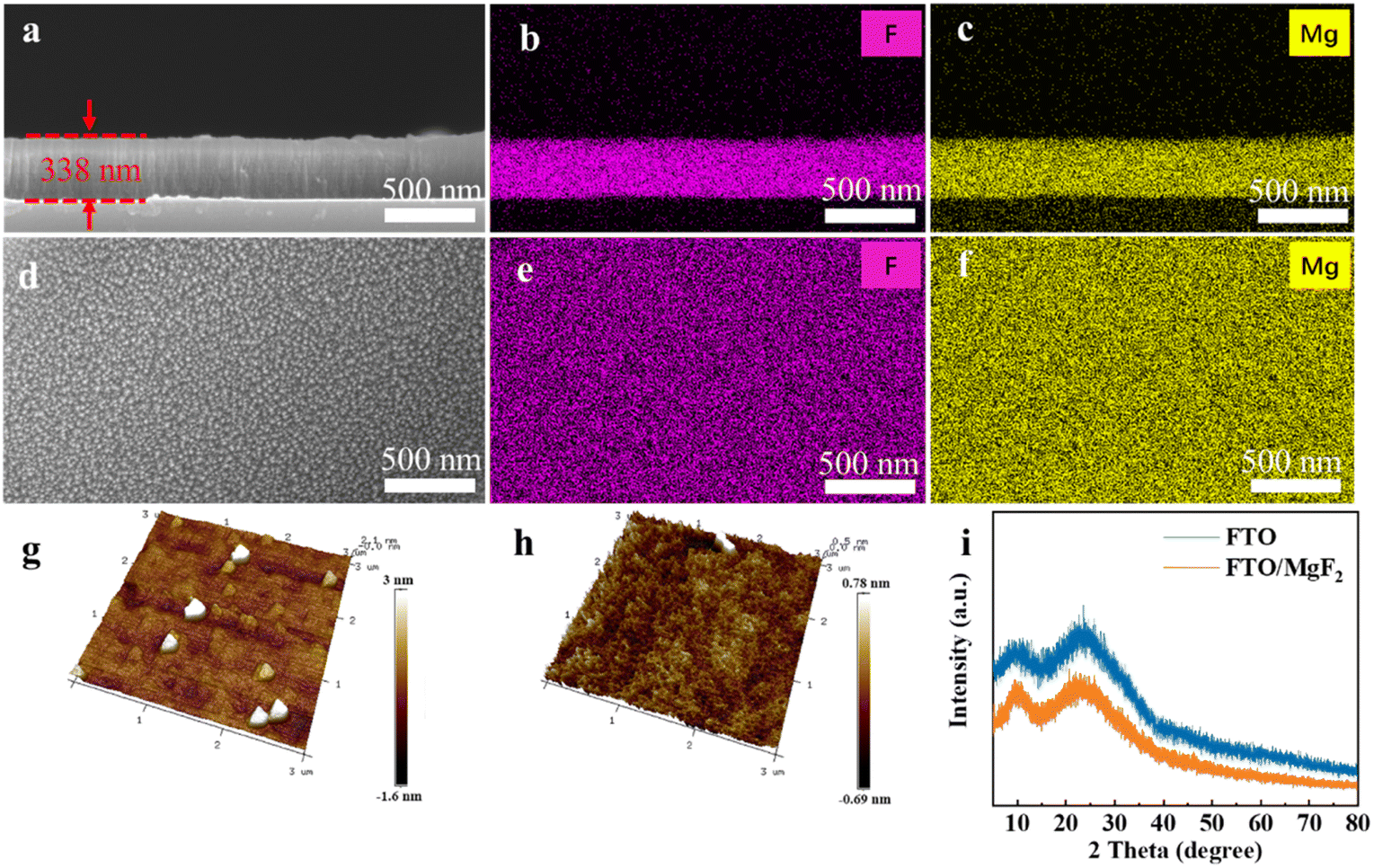 | ||
| Fig. 1 Micro-nano structures and crystalline phases. (a) Cross-sections SEM images of 300 nm MgF2 ARTF on FTO. (b) F and (c) Mg element mapping in cross-section. (d) Surface SEM image of 300 nm MgF2 ARTF on FTO. (e) F and (f) Mg element mapping on MgF2 ARTF surface. AFM topography images of FTO without (g) and with (h) MgF2 ARTF. (i) XRD patterns of FTO without and with MgF2 ARTF. | ||
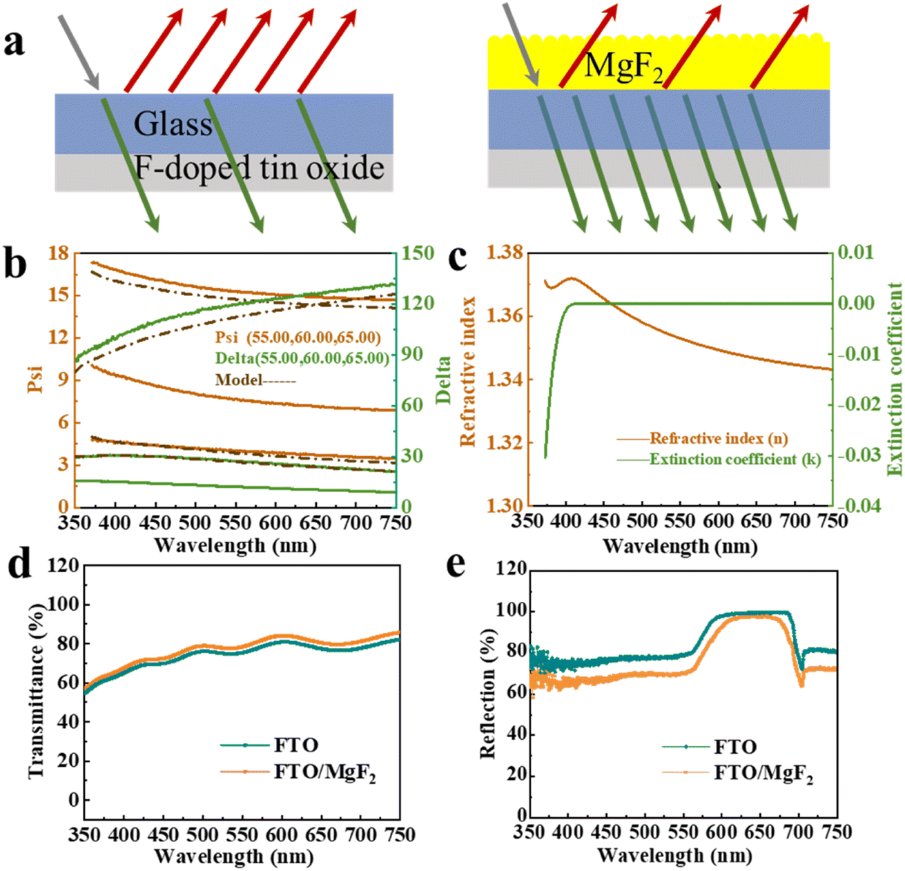 | ||
| Fig. 2 Optical properties of FTO substrate without and with MgF2 ARTF. (a) Diagram of light path in glass side of FTO without and with MgF2 ARTF. (b) Change of polarization state when the beam is reflected from the surface of MgF2 ARTF. (c) Refractive index and extinction coefficient of MgF2 ARTF on FTO. Transmission (d) and reflectance spectra (e) of FTO substrate without and with MgF2 ARTF. | ||
3.2 Optical characteristics of MgF2 ARTF
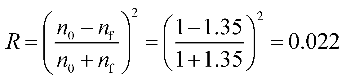
To study the optical characteristics of MgF2 ARTF, ellipsometry and reflectance and transmittance spectra were measured. Diagrams of light path in FTO without and with MgF2 ARTF are shown in Fig. 2a. The transmission spectra of MgF2 ARTF with different thicknesses (approximately 100, 330, and 560 nm) were measured, as shown in Fig. S6.† From the results of the transmission spectroscopy, it can be seen that the transmittance of MgF2 ARTF with a thickness of about 330 nm increases over the entire wavelength range (from 350 to 750 nm). Unless otherwise specified, 330 nm MgF2 ARTF were used as samples for subsequent measurements and analyses. We measured the polarization state change (psi and delta) of the beam as it reflected from the surface of the MgF2 ARTF by an M-2000VI spectroscopic ellipsometer (Fig. 2b) and calculated the simulated refractive index and extinction coefficient of the MgF2 ARTF in the wavelength range of 350–750 nm (Fig. 2c). The refractive index of MgF2 ARTF decreases gradually in the wavelength range of 410–750 nm (from 1.37 to 1.34). Theoretically, antireflective coatings can effectively reduce the reflection of light by the glass. Glass has a high refractive index of n = 1.52, so approximately 4.25% of the incident light on the surface of FTO is reflected.17 The equivalent interfacial reflectance of MgF2 ARTF can be calculated by the Fresnel equation:where R is the interface refractive index, n0 is the refractive index in the air with a general value of 1, and nf is the refractive index of the effective material (MgF2 ARTF).18 Thus, approximately 2.20% of the incident light on the surface of MgF2 ARTF is reflected. The optical properties (transmittance and reflectivity) of the MgF2 ARTF on FTO were measured from 350 to 750 nm. As can be seen from Fig. 2d and e, the transmittance of FTO with MgF2 ARTF is higher than that of bare substrate, the reflectance of FTO with MgF2 ARTF is lower than that of the bare substrate, especially in the range of 400 to 750 nm (BaSO4 as back plate for measurement of reflectivity). The above results indicate that MgF2 ARTF can reduce light reflection on the surface and increase light transmission into the device, which will help to increase the short-circuit current density and result in improving the PCE.
3.3 Effect of MgF2 ARTF on performance of inverted PSCs
To evaluate the performance of the MgF2 ARTF, they were deposited on top of the inverted PSCs by VET and their performance were measured. The process of preparing invert PSCs is described in the experimental section. The cross-sectional structure and element mapping of inverted PSCs is shown in Fig. 3a. The position of each layer is consistent with that of the detected feature element. The thickness of Au, BCP/PC61BM, perovskite, and NiOx is approximately 160, 50, 500, and 35 nm, respectively. The schematic diagram of MgF2 ARTF on inverted PSCs is shown in Fig. 3b. The PCE of the devices was measured under 100 mW cm−2 light intensity. The PCE of inverted PSCs without and with MgF2 ARTF are 18.20 and 21.28%, respectively, as shown in Fig. 3c. The detailed photovoltaic parameters are as follows: (without MgF2 ARTF) Jsc = 21.37 mA cm−2, Voc = 1.09 V, FF = 78.16%, (with MgF2 ARTF) Jsc = 24.89 mA cm−2, Voc = 1.09 V, FF = 78.47%. The average photovoltaics parameters of the devices without and with MgF2 ARTF for 20 cells are listed as follows: for the devices without MgF2 ARTF:Voc = 1.08 ± 0.02 V, Jsc = 21.45 ± 2.53 mA cm−2, FF = 0.76 ± 0.02, PCEs = 18.1 ± 1.21%; for the devices with MgF2 ARTF:Voc = 1.08 ± 0.03 V, Jsc = 24.04 ± 1.97 mA cm−2, FF = 0.76 ± 0.03, PCEs = 19.8 ± 2.27%. The significant improvement in PCE of the devices with MgF2 ARTF is caused by the improvement in short-circuit current density. The significant improvement in PCE of the devices with MgF2 ARTF is caused by the improvement in short-circuit current density. The IPCE curves of inverted PSCs are shown in Fig. 3d. Compared with that of the devices without MgF2 ARTF, the IPCE of devices with MgF2 ARTF increases significantly in the 375–840 nm range. The integrated current density from IPCE for devices without and with MgF2 ARTF is 22.09 and 24.69 mA cm−2, respectively. The results indicate that the MgF2 ARTF increases the number of photon transmission and reduces those of photon reflection. In addition, the enhancement of photocurrent density by MgF2 ARTF under different light intensities was investigated. Fig. 3e shows the curves of the Jsc ∝ Iα, where α is the exponent, which should be close to 1, I is the light intensity. The exponent α (1.122) of inverted PSCs with MgF2 ARTF is closer to 1 than that (1.205) without MgF2 ARTF, suggesting that the non-radiation recombination has been suppressed and more carriers (photogenerated electrons and holes) are inclined to be transferred to the corresponding charge transport layer (PC61BM and NiOx).19–21 The MPP (maximum power point) tracking for 300 s was performed to evaluate both devices photostability, as shown in Fig. S7.† The current density of both devices stabilizes within the first 50 s. The current density is then stable from 50 to 300 s, indicating that both devices are photostable. Finally, the device with MgF2-ARTF was measured for stability under 300 h illumination (100 mW cm−2), and the device without MgF2-ARTF as reference. The results indicate that the PCEs of both devices are close to 70% of the initial PCE after 300 h illumination (Fig. 3f). The results indicate that MgF2 ARTF only played a role in reducing reflection and increasing PCE, but did not play a role in increasing stability.
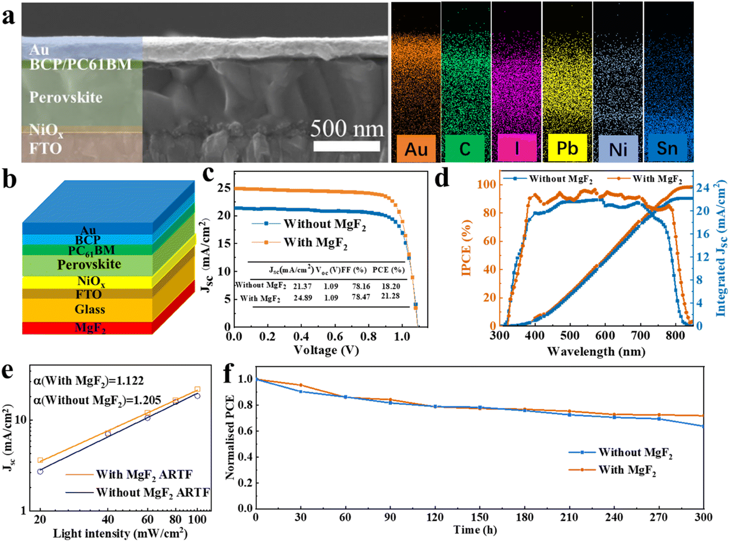 | ||
| Fig. 3 Device structure and optoelectronic performance. (a) Cross-sectional SEM image and element mapping of inverted PSCs. (b) Structure diagram of MgF2 ARTF on inverted PSCs. (c) The J–V curves of inverted PSCs without and with MgF2 ARTF. (d) The IPCE and integrated current density curves of inverted PSCs without and with MgF2 ARTF. (e) The effect of MgF2 ARTF on photocurrent density under different light intensities. (f) The stability of inverted PSCs with MgF2 ARTF under 100 mW cm−2 light intensity for 300 h illumination. | ||
4 Conclusion
In this study, different thickness amorphous MgF2 ARTF were prepared by VTE method and enhance PCE of inverted PSCs. The MgF2 films have antireflective and transmissive effects on FTO conductive glass substrates. The surface of amorphous MgF2 ARTF have a lot of nanoscale pits. The improvement in PCE of the devices with MgF2 ARTF is attributed to the improvement in short-circuit current density. VTE method can be applied to the preparation of large area MgF2 ARTF. The preparation methods and experimental conclusions in this paper can give ideas for other types of solar cells.Conflicts of interest
There are no conflicts to declare.Acknowledgements
This work was financially supported by the Shandong Province Natural Science Foundation (Grant No. ZR2019MB021).Notes and references
- K. K. Nussupov, N. B. Beisenkhanov, S. Keiinbay and A. T. Sultanov, Silicon carbide synthesized by RF magnetron sputtering in the composition of a double layer antireflection coating SiC/MgF2, Opt. Mater., 2022, 128, 112370 CrossRef CAS
.
- W. Zhang, K. Hu, J. Tu, A. Aierken, D. Xu, G. Song, X. Sun, L. Li, K. Chen, D. Zhang, Y. Zhuang, P. Xu and H. Wu, Broadband graded refractive index TiO2/Al2O3/MgF2 multilayer antireflection coating for high efficiency multi-junction solar cell, Sol. Energy, 2021, 21724, 271–279 CrossRef
- G. Y. Yoo, N. Nurrosyid, S. Lee, Y. Jeong, I. Yoon, C. Kim, W. Kim, S. Y. Jang and Y. R. Do, Newly developed broadband antireflective nanostructures by coating a low-Index MgF2 film onto a SiO2 moth-eye nanopattern, ACS Appl. Mater. Interfaces, 2020, 129, 10626–10636 CrossRef PubMed
- B. Huo, S. Jia, Y. Li, H. Zhang, C. Hao, H. Wang and S. Hu, Unveiling the effect of carbon dots on the TiO2-involved electron transport in perovskite solar cells, J. Alloys Compd., 2023, 951, 169958 CrossRef CAS
- A. Uddin, M. Upama, H. Yi and L. Duan, Encapsulation of organic and perovskite solar cells: A review, Coatings, 2019, 92, 65 CrossRef
- K. Wang, L. Zheng, Y. Hou, A. Nozariasbmarz, B. Poudel, J. Yoon, T. Ye, D. Yang, A. V. Pogrebnyakov, V. Gopalan and S. Priya, Overcoming Shockley-Queisser limit using halide perovskite platform?, Joule, 2022, 64, 756–771 CrossRef
- B. S. Richards, Comparison of TiO2 and Other Dielectric coatings for buried contact solar cells: a review, Prog. Photovolt.: Res. Appl, 2004, 124, 253–281 CrossRef
- K. Jan, P. Sven, G. Bernd, S. Mykhaylo, C. Mikaela, K. Matthias, F. Oliana, M. Stephan, A. Anna, M. Gregorii, F. Yuri and M. W. Ted, Mid-infrared optical properties of thin films of aluminum oxide, titanium dioxide, silicon dioxide, aluminum nitride, and silicon nitride, Appl. Opt., 2012, 5128, 6789–6798 Search PubMed
- Y. Wan, K. R. McIntosh and A. F. Thomson, Characterisation and optimisation of PECVD SiNx as an antireflection coating and passivation layer for silicon solar cells, AIP Adv., 2013, 33, 032113 CrossRef
- Y. Zhang, J. Zheng, C. Fang, Z. Li, X. Zhao, Y. Li, X. Ruan and Y. Dai, Enhancement of silicon-wafer solar cell efficiency with low-cost wrinkle antireflection coating of polydimethylsiloxane, Sol. Energy Mater. Sol. Cells, 2018, 181, 15–20 CrossRef CAS
- M. Gholampour, A. Miri, S. I. Karanian and A. Mohammadi, Design and fabrication of multi-layers infrared antireflection nanostructure on ZnS substrate, Acta Phys. Pol., A, 2019, 1363, 527–530 CrossRef
- X. Dai, Y. Deng, C. Van Brackle, S. Chen, P. Rudd, X. Xiao, Y. Lin, B. Chen and J. Huang, Scalable fabrication of efficient perovskite solar modules on flexible glass substrates, Adv. Energy Mater., 2020, 10, 1903108 CrossRef CAS
- B. Chen, Z. Yu, K. Liu, X. Zheng, Y. Liu, J. Shi, D. Spronk, P. Rudd, Z. Holman and J. Huang, Grain engineering for perovskite/silicon monolithic tandem solar cells with efficiency of 25.4, Joule, 2019, 3, 177–190 CrossRef CAS
- K. Bush, S. Manzoor, K. Frohna, Z. Yu, J. Raiford, A. Palmstrom, H. Wang, R. Prasanna, S. Bent, Z. Holman and M. McGehee, Minimizing current and voltage losses to reach 25% efficient monolithic two-terminal perovskite−silicon tandem solar cells, ACS Energy Lett., 2018, 3, 2173–2180 CrossRef CAS
- J. Li, Q. Dong, N. Li and L. Wang, Direct evidence of ion diffusion for the silver-electrode induced thermal degradation of inverted perovskite solar cells, Adv. Energy Mater., 2017, 714, 1602922 CrossRef
- X. Yang, D. Luo, Y. Xiang, L. Zhao, M. Anaya, Y. Shen, J. Wu, W. Yang, Y. Chiang, Y. Tu, R. Su, Q. Hu, H. Yu, G. Shao, W. Huang, T. Russell, Q. Gong, S. Stranks, W. Zhang and R. Zhu, Buried interfaces in halide perovskite photovoltaics, Adv. Mater., 2021, 33, 2006435 CrossRef CAS PubMed
- H. K. Raut, V. A. Ganesh, A. S. Nair and S. Ramakrishna, Anti-reflective coatings: A critical, in-depth review, Energy Environ. Sci., 2011, 410, 3779–3804 RSC
- J.-L. Hou, S.-J. Chang, T.-J. Hsueh, C.-H. Wu, W.-Y. Weng and J.-M. Shieh, InGaP/GaAs/Ge triple-junction solar cells with ZnO nanowires, Prog. Photovolt.: Res. Appl, 2013, 218, 1645–1652 CrossRef
- D. Glowienka and Y. Galagan, Light intensity analysis of photovoltaic parameters for perovskite solar cells, Adv. Mater., 2022, 34, 2105920 CrossRef CAS PubMed
- Y. Su, J. Yang, G. Liu, W. Sheng, J. Zhang, Y. Zhong, L. Tan and Y. Chen, Acetic Acid-assisted synergistic modulation of crystallization kinetics and inhibition of Sn2+ oxidation in tin-based perovskite solar cells, Adv. Funct. Mater., 2022, 32, 2109631 CrossRef CAS
- T. Du, W. Xu, S. Xu, S. Ratnasingham, C. Lin, J. Kim, J. Briscoe, M. McLachlan and J. Durrant, Light-intensity and thickness dependent efficiency of planar perovskite solar cells: charge recombination versus extraction, J. Mater. Chem. C, 2020, 8, 12648–12655 RSC
Footnote |
| † Electronic supplementary information (ESI) available. See DOI: https://doi.org/10.1039/d3ra08456f |
| This journal is © The Royal Society of Chemistry 2024 |