
 Open Access Article
 This Open Access Article is licensed under a Creative Commons Attribution-Non Commercial 3.0 Unported Licence
Pioneering dielectric materials of Sn-doped Nb0.025Ti0.975O2 ceramics with excellent temperature and humidity stability for advanced ceramic capacitors†
Yasumin Mingmuanga,
Narong Chanlekb,
Masaki Takesada*c,
Ekaphan Swatsitanga and
Prasit Thongbai *a
*a
aGiant Dielectric and Computational Design Research Group (GD-CDR), Department of Physics, Faculty of Science, Khon Kaen University, Khon Kaen 40002, Thailand. E-mail: pthongbai@kku.ac.th
bSynchrotron Light Research Institute (Public Organization), 111 University Avenue, Muang District, Nakhon Ratchasima 30000, Thailand
cDepartment of Physics, Hokkaido University, Sapporo, 060-0810, Japan. E-mail: mt@phys.sci.hokudai.ac.jp
First published on 4th March 2024
Abstract
In this study, the rutile TiO2 system, widely acclaimed for its superior properties, was enhanced through co-doping with isovalent Sn4+ ions and 2.5% Nb5+ donor ions, diverging from traditional acceptor doping practices. This novel doping strategy was implemented by employing a conventional solid-state reaction method, resulting in the synthesis of Sn-doped Nb0.025Ti0.975O2 (Sn-NTO) ceramics. These ceramics demonstrated remarkable dielectric characteristics, with a high dielectric constant (ε′) ranging from ∼27![[thin space (1/6-em)]](https://www.rsc.org/images/entities/char_2009.gif) 000 to 34000 and an exceptionally low loss tangent between 0.005 and 0.056 at ∼25 °C and 1 kHz. Notably, the temperature coefficient of ε′,
000 to 34000 and an exceptionally low loss tangent between 0.005 and 0.056 at ∼25 °C and 1 kHz. Notably, the temperature coefficient of ε′,  , aligned with the stringent specifications for X7/8/9R capacitors. Furthermore, the Sn-NTO ceramics exhibited a stable Cp response across various frequencies within a humidity range of 50 to 95% RH, with ΔCp (%) values within ±0.3%, and no hysteresis loop was detected, suggesting the absence of water molecule adsorption and desorption during humidity assessments. This behavior is primarily attributed to the effective suppression of oxygen vacancy formation by the Sn4+ ions, which also affects the grain growth diffusion process in the Sn-NTO ceramics. The observed heterogeneous electrical responses between semiconducting grains and insulating grain boundaries in these polycrystalline ceramics are attributed to the internal barrier layer capacitor effect.
1. Introduction
Over the past two decades, research on dielectric materials has been continuously reported and extensively discussed due to their intriguing performance in advanced electronic devices. Among various applications, capacitors stand out as primary beneficiaries of these materials, owing to their high dielectric response (ε′ > 104). In 2000, Subramanian et al. unveiled the discovery of materials with giant dielectric permittivity (GDP), including CaCu3Ti4O12 (CCTO) and its related compounds ACu3Ti4O12. These materials exhibited an outstanding ε′, with CCTO achieving ∼12000 at room temperature (RT) and at a frequency of 1 kHz.1 The primary cause of high ε′ is attributed to interfacial polarization, arising from distinct electrical responses between semiconducting grains and insulating grain boundaries. This phenomenon is known as the internal barrier layer capacitor (IBLC) model.2,3 Unfortunately, CCTO still exhibited low stability of ε′ at high temperatures, which is a disadvantage for application in the industrial sector. This issue is similar to the challenges faced by traditional BaTiO3 materials and other GDP materials.4–7
Up until 2013, the excellent performance in dielectric properties were observed in the form of a simple material based on rutile TiO2.8–11 These improvements were achieved by introducing acceptor (A) and donor (D) dopants, which influenced the generation of defects within the structure of TiO2. The substitution of D dopants (i.e., Nb5+) led to an increase in the ε′ value due to the reduction of Ti4+ to Ti3+, forming a diamond-shaped structure. Conversely, the introduction of A dopants, like In3+, resulted in a triangular shape. This defect was used to explain the reduction of loss tangent (tanδ) value. Surprisingly, the stability of ε′ was obtain over a wide temperature range from −193 to 177 °C. When both of these shapes overlapped, the ceramics exhibited excellent performance, a phenomenon referred to as the Electron-pinned defect-dipoles (EPDD) model.8,12,13 However, the mechanism underlying the behavior of TiO2-based materials remained a topic of debate, with many reports suggesting the origin of these ceramics might be related to the IBLC effect, akin to GPD materials such as CCTO ceramics.14–17
Most recently, we presented our findings on the co-doping of TiO2 with Sn4+ and Ta5+ under the phenomenon of the IBLC model.16 This co-doping system resulted in excellent dielectric properties, with high ε′ and low tanδ as well as a stable ε′ performance across a wide temperature range, making them well-suited for application in ceramic capacitors. Furthermore, we developed (Sn0.5Nb0.5)xTi1−xO2+x/4 ceramics with x values of 0.01, 0.025, and 0.05, demonstrating noteworthy GDP performance.18 Notably, these dense ceramics were achieved at lower sintering temperatures compared to other co-doped TiO2 systems. According to the previous works, the primary role of Sn4+ in achieving these remarkable properties was attributed to its ability to inhibit the formation of oxygen vacancies.16,19 Substituting Sn4+ ions in CCTO or co-doped TiO2 materials helps minimize free electron generation from oxygen loss during sintering. However, the specific influence of varying Sn4+ concentrations on the dielectric GDP performance of Sn4+ and Nb5+ co-doped TiO2 remains unexplored. The EIA standard for ceramic capacitors specifies that dielectric constant variations should remain below 15% across a defined temperature range for X–R type capacitors. This standard highlights the necessity for materials to exhibit minimal capacitance (Cp) fluctuation in response to temperature shifts or other external factors, such as humidity. Despite this, the impact of humidity—a critical consideration in capacitor performance—has scarcely been reported. Variations in dielectric properties induced by humidity can severely impair capacitor functionality, particularly under high relative humidity (RH) conditions. Previous studies on CCTO and other co-doped TiO2 materials, such as those incorporating In3+ and Na+/Nb5+, have demonstrated significant dependence of Cp and ε′ values on RH levels.20–22 This suggests that water molecules may interact with the ceramic, leading to substantial permittivity increases and indicating intrinsic defect presence.
For co-doped TiO2, the creation of defects like oxygen vacancies has been highlighted as a crucial factor in water molecule adsorption/desorption, influencing Cp and ε′ changes with humidity. Such Cp variations are undesirable for capacitor use, suggesting a need for further investigation. We hypothesize that Sn4+ and Nb5+ co-doped TiO2 will not only exhibit high GDP and low tanδ, but will also demonstrate stability across temperature and humidity variations. Thus, this study aims to delve deeper into the role of co-doping in TiO2 materials, enhancing the reliability and efficacy of ceramic capacitors under diverse environmental conditions. Our findings aim to contribute significantly to the field, offering insights into material behaviors that could lead to advancements in capacitor technology.
In this work, we synthesized Sn4+ and Nb5+ co-doped rutile TiO2 with varying Sn4+ concentrations using a standard solid-state reaction (SSR) method and sintered the samples at 1200 °C for 3 h. Phase composition, microstructure, and oxidation state were investigated using specific techniques. Importantly, we measured dielectric and electric properties under various conditions, including different frequencies and temperatures. Surprisingly, excellent stability of ε′ or Cp was simultaneously obtained over a wide temperature range from −60 to 210 °C and humidity range from 50 to 95% RH in all ceramics, respectively. Furthermore, the origin of the dielectric property in these ceramics will be discussed from the perspective of impedance spectroscopy.
2. Experimental details
The rutile TiO2 ceramics, doped with Nb5+ and Sn4+ ions, were synthesized using the SSR method. The raw materials, including high-purity oxides of SnO2 (99.9% purity, Sigma-Aldrich, UK), Nb2O5 (99.99% purity, Sigma-Aldrich, China), and TiO2 (≥99.9% purity, Sigma-Aldrich, Japan), were carefully weighed according to the stoichiometric ratios required for SnxNb0.025Ti0.975−xO2 (Sn-NTO) ceramics with varying Sn4+ concentrations (x = 1, 2.5, and 5%, denoted as 1% Sn-NTO, 2.5% Sn-NTO, and 5% Sn-NTO, respectively). First, these raw materials were thoroughly mixed in ethanol using ZrO2 balls (2.0 mm in diameter) for 24 h to ensure a homogeneous blend. Second, the ZrO2 balls were separated from the mixtures of raw materials in ethanal. Third, the resulting wet mixtures were dried in the drier at ∼80 °C to evaporate ethanol. After drying, the resultant powders were then finely milled and pressed into green bodies with 5% polyvinyl alcohol (PVA) under a uniaxial pressure of 250 MPa. The formed pellets measured 0.95 mm in diameter and 1.2 mm in thickness. Finally, all green bodies were loaded onto an alumina plate and coved by a large crucible. Finally, these green bodies were placed on an Al2O3 plate, covered with a large crucible, and sintered at 1200 °C for 3 h in an air atmosphere, with a ramp rate of 5 °C min−1, followed by natural cooling to ambient temperature. The densities of the sintered specimens were determined using the Archimedes method.Subsequently, the sintered Sn-NTO ceramics were comprehensively characterized using various techniques. Empyrean X-ray diffraction (XRD) from PANalytical was utilized to investigate the crystal structure, phase composition, and purity of the samples. The results were further confirmed using a micro-Raman system (Horiba Jobin Yvon T64000). The microstructure and elemental mapping of the ceramics were analyzed through field-emission scanning electron microscopy (FESEM) with energy-dispersive X-ray spectroscopy (EDS) using Helios NanoLab, G3 CX instrument. To determine the charge composition and the presence of ions in various states on the ceramic's surface, X-ray photoelectron spectroscopy (XPS) was employed. This analysis was carried out using a PHI5000 VersaProbe II instrument, which was supported by the Synchrotron Light Research Institute (SLRI) in Thailand.
To investigate the dielectric and electrical responses of Sn-NTO ceramics without the surface effects, both sides of the samples were ground using sandpaper and subsequently painted with silver (Ag) to create parallel electrodes. The samples were then heated to 600 °C for 0.5 h, with a heating rate of 5 °C min−1. Dielectric properties, ε′ and tanδ, were measured using an impedance analyzer (KEYSIGHT E4990A) across a wide frequency range (102 to 106 Hz) and over a temperature range of −60 to 210 °C under Vrms = 0.5 V. Subsequently, each humidity response in the Sn-NTO ceramics was evaluated at 25 °C by measuring adsorption and desorption in the range 50 to 95% RH at different frequencies using a humidity chamber (ESPEC, SH-222).
3. Results and discussion
To study phase composition and crystal structure of rutile TiO2 ceramics after doping with Nb5+ and Sn4+ ions, XRD patterns of the sintered 1% to 5% Sn-NTO ceramics are revealed in Fig. 1(a). The phase compositions of the samples were identified as only the tetragonal rutile TiO2 phase, according to (No. JCPDS 21-1276).15,23 In other words, no impurity phases were detected. Complementing the XRD results, the SEM-EDS mapping images demonstrate a uniform distribution of all constituent elements in the 5% Sn-NTO ceramic, which represents the highest doping concentration of Sn4+. This uniformity is clearly evident, as there is no discernible segregation or accumulation of a second phase, especially at the grain boundaries, as depicted in Fig. S1 of the ESI.† Thus, XRD and SEM-EDS mapping can be used to confirm the existence of a single rutile TiO2 phase in the Sn-NTO ceramics. As presented in Fig. 1(b), the 2θ of (110) diffraction peaks, the strongest peak, shifted toward lower angles when Sn4+ concentrations increased, which is similar to other works.14,23,24 The results were attributed to the increasing lattice parameters (a and c) and bond lengths of the crystal. Additionally, it is important to note that the apparent splitting of the (110) peak at higher 2θ values can be attributed to the Kα2 component of the Cu radiation source used in the XRD analysis. This phenomenon is a well-recognized artifact stemming from the doublet nature of Cu-Kα radiation, wherein the Kα1 and Kα2 emission lines produce two peaks that are closely spaced. | ||
| Fig. 1 (a) XRD patterns of the Sn-NTO ceramics. (b) Enlarged peak of (110). | ||
Accurate determination of the structural parameters was achieved through Rietveld refinement using the X'pert HighScore Plus software, with the refined patterns displayed in Fig. S2 (ESI†). The derived lattice constants and bond lengths are compiled in Table S1 (ESI†), and key findings are concisely presented in Table 1. It is observed that both the lattice parameters (a and c) and the bond lengths (A–O and A–A, where A = Ta, Sn, Ti) incrementally increase with higher concentrations of Sn4+. This trend can be attributed to the substitution of Ti4+ sites by the larger ionic radii of Sn4+ (69.0 pm) and Nb5+ (64.0 pm), compared to that of Ti4+ (60.5 pm).The systematic enlargement of these structural parameters is indicative of a complete and homogeneous integration of the dopants into the host lattice, as supported by the data.15,16
δ) at 1 kHz and 25 °C and temperature coefficient  for 1% Sn-NTO, 2.5% Sn-NTO, and 5% Sn-NTO ceramics
| Sample | Dielectric properties @ 1 kHz & 25 °C | Temperature range for
|
|
|---|---|---|---|
| ε′ | tanδ |
||
| 1% Sn-NTO | 33853 |
0.005 | −60 to 210 °C |
| 2.5% Sn-NTO | 31629 |
0.015 | −60 to 210 °C |
| 5% Sn-NTO | 27159 |
0.056 | −60 to 210 °C |

Raman spectroscopy is an analytical technique used to investigate the chemical composition and molecular structure of materials by measuring changes in the frequency of vibrational and rotational modes in the sample. Raman spectra of the Sn-NTO samples were observed in the range 120 to 700 cm−1, as illustrated in Fig. S3 (ESI†). The results in the Sn-NTO samples revealed the spectra consisting of four peaks (generally three peaks and a second-order Raman scattering in the rutile structure) similar to in the rutile TiO2.14,24 Therefore, the confirmation of the exclusive presence of rutile TiO2 in the Sn-NTO samples was supported by XRD, mapping image of elements, and Raman spectroscopy. Each peak indicated a different response of structure. These shifts were fitted and calculated using the Lorentz model. Interestingly, the two strongest peaks corresponding to the Eg and A1g modes shifted when the Sn4+ concentrations were varied, as shown in the inset of Fig. S3 (ESI†) and listed in Table S1 (ESI†). The Eg modes shifted to lower energy side in the range of 439 to 437 cm−1 as the Sn concentration increased, which can be attributed to certain factors such as lattice distortion and the movement of oxygen along c-axis.14 Meanwhile, the A1g modes showed a slight shift to higher frequency side in the range of 606 to 607 cm−1 related to the change in the Ti–O stretch modes after the replacement of Ti with Sn and Nb.15,24
The Ti 2p profile in the 5% Sn-NTO sample is presented in Fig. 2(a). It revealed two distinct peaks of Ti 2p3/2, located at binding energies of 457.02 eV and 458.64 eV, corresponding to Ti3+ and Ti4+ states, respectively.8 Additionally, at higher binding energies, the Ti 2p1/2 peaks associated with Ti3+ and Ti4+ states exhibited lower intensity peaks at 462.68 eV and 464.30 eV, respectively.15,24 The presence of Ti3+ within the structures can be attributed to charge compensation, whereby Ti4+ was converted into Ti3+ through donor doping with Nb5+. This phenomenon was described by eqn (1) and (2) as follows:
 | (1) |
| Ti4+ + e → Ti3+ | (2) |
 | ||
| Fig. 2 XPS spectra of (a) Ti 2p, (b) O 1s, and (c) Sn 3d for 5% Sn-NTO ceramic. | ||
In accordance with previous work, the quantity of Ti3+ within the structure played a crucial role in determining the dielectric response.8,16 Theoretically, the Ti3+/Ti4+ ratio in the 5% Sn-NTO ceramic should be approximately 2.7%, which closely aligned with the experiment result of 2.5% calculated from the theoretical value from the nominal formula.
As depicted in Fig. 2(b), the three components of O 1s in the 5% Sn-NTO sample were determined using Gaussian–Lorentzian profile fitting. The primary peak corresponds to oxygen lattice, representing the bulk Ti–O bond, and it was detected at a binding energy of 530.04 eV.14 Additionally, two other components, associated with oxygen vacancies and hydroxyl (OH) groups, were observed as peaks at 531.54 and 532.79, respectively.8,14 The ratio of oxygen vacancies to the main oxygen lattice in 5% Sn-NTO ceramic was calculated to be 15.6%. This result can be attributed to the sintering process, without the influence of dopants such as Nb5+ and Sn4+ on the generation of oxygen vacancies.16 In other words, Nb5+ solely affected the presence of free electrons, while Sn4+ contributed to the suppression of oxygen vacancy formation, in accordance with eqn (3).
 | (3) |
Furthermore, the ratio of duplication 15.6% is lower than the value of 18.9% obtained in our previous study for 2.5% Sn-NTO (or 5% Sn-NTO) ceramic with a difference of about 3.3%.18 This result indicated that Sn4+ ions inhibit the oxygen loss in the ceramic structure, which is consistent with the influence of Sn4+ in CCTO ceramics.19
In contrast, when doping TiO2 with A2+/3+ such as Cr3+, Zn2+, and In3+, it is generally expected to create oxygen vacancies for charge compensation.8,15,23 To confirm the presence of only Sn4+ state (without Sn2+ state) in the structure of the 5% Sn-NTO sample, the Sn 3d profile was observed in detail with binding energies of 486.48 and 494.92 eV, corresponding exclusively to the existence of Sn4+, as shown in Fig. 2(c).25 Therefore, there is no oxygen loss attributed to Sn2+ ions in Sn-NTO ceramics. In the previous work,18 it was observed that both Sn2+ and Sn4+ were detectable in the 2.5% (Sn0.5Nb0.5) co-doped TiO2. In contrast, in the current study, only Sn4+ was identified in the 5% Sn-doped Nb0.025Ti0.975O2 (5% Sn-NTO), as indicated by the fitting results and the notably lower FWHM values of the Sn 3d peaks. The increased sharpness and symmetry of these peaks in our XPS analysis suggest a more homogeneous chemical environment, which is likely indicative of a predominance of Sn4+ ions. A higher doping level, such as that in the 5% Sn-NTO, could lead to a more pronounced alteration or lattice distortion within the rutile TiO2 structure, thus potentially stabilizing the Sn4+ oxidation state. Additionally, the formation and distribution of oxygen vacancies in the TiO2 lattice—arising from oxygen loss during the sintering process—are critical factors that can stabilize different oxidation states of the dopants, as supported by eqn (3).
The surface morphologies of Sn-NTO ceramics are presented in Fig. 3, with their insets displaying the statistical distribution grain sizes. The relative density and grain size of each Sn-NTO sample were also calculated and are listed in Fig. 3(d). A high relative density and a small number of pores were achieved in the 1% Sn-NTO and 2.5% Sn-NTO ceramics, measuring approximately 97.35% and 98.71%, respectively, as depicted in Fig. 3(a) and (b). Unfortunately, higher concentration of Sn (5% Sn-NTO) resulted in lower density (95.48%), with value below those of the 1% Sn-NTO and 2.5% Sn-NTO ceramics, approximately 1.9% and 3.3%, respectively, with corresponding increased porosity, as show in Fig. 3(c). Moreover, the reduction in grain growth was observed as the Sn4+ concentrations increased, decreasing from 3.6 to 2.7 μm in Fig. 3(d). These results might primally be caused by the influence of SnO2 properties. SnO2 was characterized by its low densification during the sintering process, which was used in advanced applications for humidity sensor devices.26 It was observed that the mean grain size in Ga3+-doped TiO2 exceeded that of the undoped TiO2, a phenomenon primarily ascribed to the generation of oxygen vacancies for charge compensation.27 This implies that oxygen vacancies facilitate improved diffusion within the microstructure, consequently resulting in a reduced density and a diminishment in grain size. In our preceding research involving (Sn0.5Nb0.5) co-doped TiO2 ceramics, we documented the coexistence of Sn2+ alongside Sn4+.18 The presence of Sn2+ ions within the TiO2 matrix is ionically compensated by oxygen vacancies, which promotes the diffusion of ions and/or atoms across the grain boundaries, thereby fostering grain growth and higher ceramic densities.18 However, the current study found no evidence of the Sn2+ state in the Sn-NTO ceramics structure, as demonstrated by the XPS results. This absence likely accounts for the relatively higher densities observed in the (Sn0.5Nb0.5) co-doped TiO2 ceramics compared to the Sn-NTO ceramics presented herein.18 Additionally, it is noteworthy that the highest concentration of Sn4+ doping corresponded with the lowest relative density among the Sn-NTO samples examined. Nevertheless, the density in all obtained Sn-NTO ceramics is suitable for advanced applications and demonstrated excellent properties, as reported in other works, such as Tm3+/Ta5+ co-doped TiO2 and In3+/Zr4+/Nb5+ triple-doped TiO2.28,29 This was primarily attributed to the diffusion during the thermal sintering process.
 | ||
| Fig. 3 Surface morphologies of (a) 1% Sn-NTO, (b) 2.5% Sn-NTO, and (c) 5% Sn-NTO ceramics, respectively. (d) Grain sizes and relative density values of the Sn-NTO samples. | ||
Generally, the ε′ response is often influenced by the D5+ (e.g., Nb5+ and Ta5+) effect. As the concentration of D5+ doping increases, the ε′ value also tends to increase because D5+ can induce free electrons within the structure, as described in eqn (1) and (2). The increased presence of free electrons serves as a key contributor to the enhancement of both intrinsic polarization at the local complex defect cluster and interfacial polarization at interfaces and grain increase within these materials.8,15 However, the Nb5+ concentration was prepared and mixed at the same level, x = 0.025, for the Sn-NTO samples. As a result, there should be no significant increase or alteration in ε′ performance owing to the uniform Nb5+ concentration. Surprisingly, the ε′ response in the frequency range of 102 to 106 Hz at 25 °C decreased with increasing Sn4+ concentrations in Fig. 4. Compared to the 1% Sn-NTO and 2.5% Sn-NTO samples, a significant decrease was observed at the highest concentration of Sn4+ in the 5% Sn-NTO sample, as shown in Fig. 4. The results indicated the influence of Sn4+ and the microstructure, including factors such as grain sizes and the presence of porosity in the ceramics.16,18 The reduction in grain sizes can lead to a decrease in ε′ performance, in according with the IBLC model.16 Regarding the impact of porosity, these models consider the dielectric material as a composite system consisting of two phases, a matrix with numerous pores, each having different ε′ values or responses. The existence of air or other non-dielectric voids within the material creates regions with ε′ values lower than those of the bulk material.30 As a result, the effective ε′ of the porous material decreases, which may be another contributing factor to the lowest ε′ value observed in the 5% Sn-NTO ceramic. As shown in the inset of Fig. 4, the tanδ values were dependent on the frequency range of 102 to 106 Hz at 25 °C for the 5% Sn-NTO ceramics. The results indicated an increase in tanδ as Sn4+ concentrations rose, especially in 2.5% Sn-NTO and 5% Sn-NTO ceramics at a low frequency, which can be attributed to relaxation peaks. However, ε′ and tanδ values for the Sn-NTO samples remained consistently high, exceeding 104 and staying below 0.06 at 25 °C and 1 kHz, respectively, as listed in Table 1. Moreover, the rapid decline in ε′ response at high frequencies was attributed to the Maxwell–Wagner relaxation, a phenomenon that correlated with the IBLC model.3,18 Further discussion is provided in the impedance results.
 | ||
| Fig. 4 Frequency dependence of ε′ at 25 °C of Sn-NTO ceramics sintered at 1200 °C for 3 h; the inset shows the tanδ. | ||
Ceramic materials, known for their exceptional high chemical, mechanical, and thermal stability, are widely employed in advanced devices, which are particularly suitable for use in extreme environments. In the context of their application in X–R type ceramic capacitors, as defined by the Electronics Industries Alliance (EIA), the stability of dielectric properties across a range of temperatures is of utmost importance. These capacitors must adhere to strict criteria, such as the temperature coefficient of capacitance at 1 kHz (ΔC/C25 (%), where C25 represents capacitance at 1 kHz and 25 °C) or the temperature coefficient of ε′ ( , where
  is the dielectric constant at 1 kHz and 25 °C), which must remain within a ±15% tolerance over a wide temperature range between −55 to 125 (X7R), −55 to 150 (X8R), and −55 to 200 °C (X9R), respectively.31 As illustrated in Fig. 5(a), the
  for 1% Sn-NTO and 2.5% Sn-NTO ceramics were relatively independent of temperature at 1 kHz, indicating only slight changes in ε′ values at different temperatures. Meanwhile, the 5% Sn-NTO ceramic exhibited
  at 1 kHz that depended on temperatures, which was related to in tanδ response, especially at high temperatures, as shown in Fig. 5(b). The
  at 1 kHz for all Sn-NTO ceramics remained below ±15% tolerance range between −60 to 210 °C, as summarized in Table 1. This demonstrates their compatibility with the X–R types of ceramic capacitors, specifically X7R, X8R, and X9R. For these capacitor types, the
  is required to stay within ±15% across their respective temperature ranges of −55 to 125 °C, −55 to 150 °C, and −55 to 200 °C. In addition to the low
  values within these specified ranges, it is also essential for the tanδ values to remain low for the application in X7R, X8R, and X9R capacitors. Notably, the tanδ values for both 1% Sn-NTO and 2.5% Sn-NTO samples were also slightly temperature-dependent, but they remained below 0.05 over a wide temperature range of −60 to 210 °C. This excellent property allows Sn-NTO ceramics to be considered as candidates for application in advanced devices in the future, especially when compared to traditional BaTiO3 and CCTO-related materials.4,32–34
 | ||
Fig. 5 Temperature dependence of (a)  and (b) tanδ of 1% Sn-NTO, 2.5% Sn-NTO, and 5% Sn-NTO ceramics sintered at 1200 °C for 3 h at 1 kHz. and (b) tanδ of 1% Sn-NTO, 2.5% Sn-NTO, and 5% Sn-NTO ceramics sintered at 1200 °C for 3 h at 1 kHz. | ||
In previous research, it was observed that the humidity in the environment can impact the dielectric properties, such as ε′ or the capacitance (Cp), in dielectric materials.21,22,35,36 The changes of these properties indicate the adsorption of water molecules into the ceramic structure, leading to enhanced polarization related to Cp or ε′ response. These results should be affected by the presence of intrinsic defects such as oxygen vacancies and  ions, as well as microstructure effects.21,37 This phenomenon has been widely applied in humidity sensors. However, for the application of ceramic capacitors, it is essential to maintain the stability of Cp or ε′ over a wide range of relative humidity conditions, similar to the previous result for
  . As shown in Fig. 6(a) and (b), the Cp responses of 1% Sn-NTO and 5% Sn-NTO ceramics at various frequencies (100 to 100 kHz) showed an independent response to changes in relative humidity (% RH) within the range of 50 to 95%. However, a significant reduction in Cp was observed at high frequencies. This reduction is due to the polarization process not being able to keep up with the rapidly changing electric field, which is a normal behavior of dielectric response.38,39 Furthermore, there was no hysteresis observed in the adsorption and desorption of water molecules in the Sn-NTO samples. The humidity coefficient of capacitance was calculated using ΔCp (%) = [(CRH − C50)/C50] × 100, where CRH and C50 are the capacitance at any % RH and 50% RH, respectively. The ΔCp (%) values for both the 1% Sn-NTO and 5% Sn-NTO ceramics were lower than ±0.3% at different frequencies of 1, 10, and 100 kHz, as shown in the insets of Fig. 6(a) and (b). These results indicated that there was no adsorption and desorption of water molecules and no substantial increase in polarization in Sn-NTO ceramics. This phenomenon was attributed to the inhibition of oxygen loss in structure due to the Sn4+ effect.19,22 Surprisingly, the microstructural differences in grain sizes and porosity did not result in different Cp responses in 1% Sn-NTO and 5% Sn-NTO ceramics. This finding was aligned with the previous research on Mg-doped CCTO ceramics.36 In considering a dielectric material for humidity sensor applications, the sensitivity of the ceramics was calculated using the equation: sensitivity = ΔCp/Δ(% RH),21,40 where ΔCp and Δ(% RH) denote the changes in capacitance and relative humidity, respectively. As illustrated in Fig. 6(c), while the high sensitivity values of (In + Nb) and (Na + Nb) co-doped TiO2 are advantageous for humidity sensor applications, the markedly low sensitivity observed in Sn-NTO ceramics demonstrates their superior dielectric stability, making them highly suitable for capacitor applications.
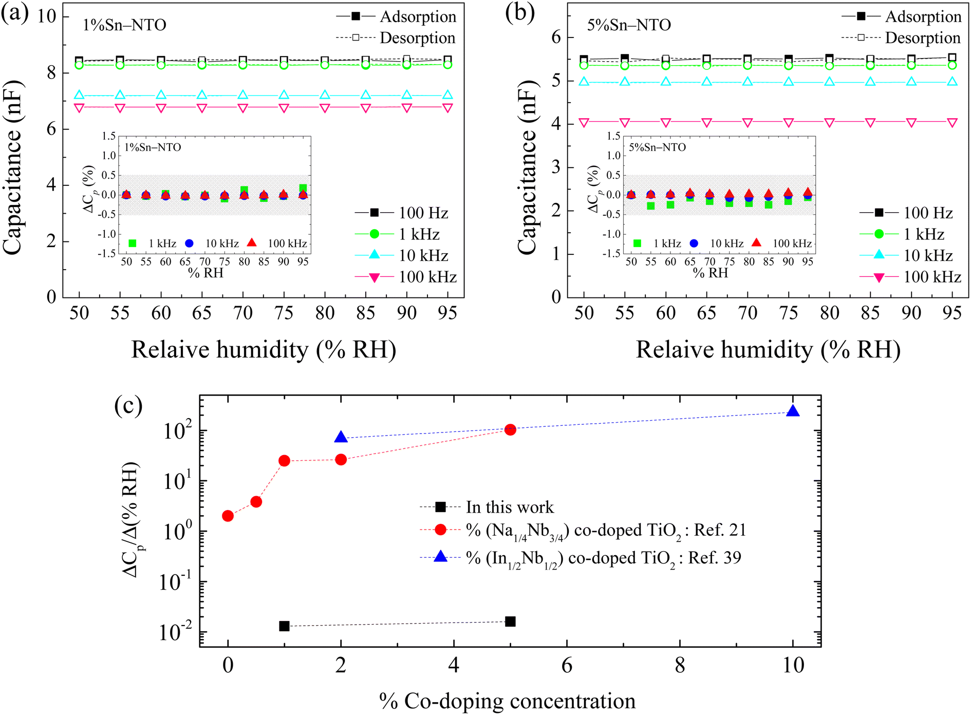 | ||
| Fig. 6 Relative humidity dependence of Cp at 25 °C and several frequencies for (a) 1% Sn-NTO and (b) 5% Sn-NTO; their insets show the ΔCp (%). (c) Comparison of Cp-humidity sensitivity of Sn-NTO with (In + Nb) and (Na + Nb) co-doped TiO2 ceramics. | ||
Based on the IBLC model, impedance spectroscopy was employed to elucidate the origin of the excellent dielectric properties in the Sn-NTO ceramic samples, particularly in the context of their application in ceramic capacitors. As shown in Fig. 7, the complex impedance plane (Z*) plots for the Sn-NTO samples at 180 °C revealed large semicircular arcs corresponding to the insulating components, such as surface layer and/or grain boundaries.2,15,41,42 However, it is important to note that only insulating grain boundaries were present in the Sn-NTO samples, as the surface of the samples was intentionally removed before making the electrodes and then measuring dielectric properties. At 25 °C, smaller semicircular arcs were observed at the high frequencies, representing the response of the semiconducting part of the grains, as illustrated in the inset of Fig. 7.3 The diameter of these semicircular arcs can be used to consider the resistance values of each electrical response part.7,17,24 Furthermore, the grain boundary resistance (Rgb) value is significantly large compared to the grain resistance (Rg) value and Rgb of other GDP materials, which contributed to achieving both low tanδ value and  value within ±15% over a wide range.6,42,43 Meanwhile, the Rg values were on the order of ∼102 and decreased with increasing Sn4+ concentrations. This result indicates the decrease of ε′ response associated with the increase of Sn4+ concentrations. These responses in the preset polycrystalline Sn-NTO ceramics are considered to be a phenomenon caused by the IBLC model.
 | ||
| Fig. 7 Z* plots for Sn-NTO samples at 180 °C and over a wide frequency range of 102 to 106 Hz; the inset shows Z* plots at 25 °C near the origin at high frequencies. | ||
4. Conclusions
The Sn-NTO ceramics were synthesized via the SSR method, sintered at 1200 °C for 3 h in an air atmosphere. These ceramics exhibited a pure tetragonal rutile TiO2 phase without impurities, as confirmed by XRD and Raman spectroscopy analyses. XPS results supported the formation of Ti3+ ions within the Sn-NTO ceramics, significantly influencing the dielectric response. Interestingly, the grain growth in these ceramics was found to be dependent on the Sn4+ ion concentration. Remarkably, the Sn-NTO samples demonstrated outstanding performance, making them suitable for use in X–R type ceramic capacitors designed for extreme environmental conditions. These ceramics showcased not only a low tanδ at 1 kHz and 25 °C, but also stable dielectric responses across a wide temperature range, and they maintained constant Cp responses under varying humidity levels. These results showed the pivotal role of Sn4+ ions in minimizing oxygen vacancy-related losses within the ceramic structure. Impedance spectroscopy analysis revealed that the distinctive properties of the Sn-NTO ceramics could be attributed to extrinsic effects, as described by the IBLC model.
Conflicts of interest
There are no conflicts to declare.Acknowledgements
This research project is supported by National Research Council of Thailand (NRCT): (N41A640084 and N41A640193). This study was partly supported by Hokkaido University, Grant-in-Aid for Scientific Research (B) (21H01107). This research work was also supported by the Research and Graduate Studies Office of Khon Kaen University. The authors would like to thank the SUT-NANOTECSLRI (BL5.3) Joint Research Facility for use of their XPS facility. Y. M. would like to thank the National Research Council of Thailand under The Royal Golden Jubilee PhD Program for her PhD scholarship.References
- M. A. Subramanian, D. Li, N. Duan, B. A. Reisner and A. W. Sleight, J. Solid State Chem., 2000, 151, 323–325 CrossRef CAS.
- D. C. Sinclair, T. B. Adams, F. D. Morrison and A. R. West, Appl. Phys. Lett., 2002, 80, 2153 CrossRef CAS.
- J. Liu, C.-G. Duan, W.-G. Yin, W. Mei, R. Smith and J. Hardy, Phys. Rev. B: Condens. Matter Mater. Phys., 2004, 70, 144106 CrossRef.
- H. Gong, X. Wang, S. Zhang, H. Wen and L. Li, J. Eur. Ceram. Soc., 2014, 34, 1733–1739 CrossRef CAS.
- H. Chandra Rao Bitra, A. V. Rao, K. S. Babu and G. N. Rao, Mater. Chem. Phys., 2020, 254, 123379 CrossRef CAS.
- S. Kumar, S. Supriya, L. K. Pradhan and M. Kar, J. Mater. Sci.: Mater. Electron., 2017, 28, 16679–16688 CrossRef CAS.
- J. Boonlakhorn, N. Chanlek, J. Manyam, P. Srepusharawoot, S. Krongsuk and P. Thongbai, J. Adv. Ceram., 2021, 10, 1243–1255 CrossRef CAS.
- W. Hu, Y. Liu, R. L. Withers, T. J. Frankcombe, L. Norén, A. Snashall, M. Kitchin, P. Smith, B. Gong, H. Chen, J. Schiemer, F. Brink and J. Wong-Leung, Nat. Mater., 2013, 12, 821–826 CrossRef CAS.
- K. Safeen, R. Ullah, A. Safeen, Zulfiqar, M. Kabeer, R. Khan, H. Ullah, A. Zaman, K. Shafique Ahmad, M. Z. Ullah Shah, H. O. Elansary, I. Mohamed Moussa, R. Casini and E. A. Mahmoud, J. Saudi Chem. Soc., 2023, 27, 101711 CrossRef CAS.
- X. Wang, B. Zhang, L. Xu, X. Wang, Y. Hu, G. Shen and L. Sun, Sci. Rep., 2017, 7, 8517 CrossRef PubMed.
- T. Nachaithong, W. Tuichai, P. Kidkhunthod, N. Chanlek, P. Thongbai and S. Maensiri, J. Eur. Ceram. Soc., 2017, 37, 3521–3526 CrossRef CAS.
- L. Wang, J. Li, X. Liu, M. Zhang, X. Li, S. Liu and X. Sun, Ceram. Int., 2023, 49, 32116–32126 CrossRef CAS.
- W. Dong, W. Hu, T. J. Frankcombe, D. Chen, C. Zhou, Z. Fu, L. Candido, G. Hai, H. Chen, Y. Li, R. L. Withers and Y. Liu, J. Mater. Chem. A, 2017, 5, 5436–5441 RSC.
- L. Zhou, Z. Peng, J. Zhu, Q. Shi, P. Liang, L. Wei, D. Wu, X. Chao and Z. Yang, Mater. Chem. Phys., 2023, 295, 127072 CrossRef CAS.
- W. Tuichai, S. Danwittayakul, N. Chanlek, M. Takesada, A. Pengpad, P. Srepusharawoot and P. Thongbai, ACS Omega, 2021, 6, 1901–1910 CrossRef CAS.
- Y. Mingmuang, N. Chanlek, V. Harnchana and P. Thongbai, Ceram. Int., 2023, 49, 188–193 CrossRef CAS.
- L. Zhou, G. Yang, D. Yang, J. Xu, Z. Peng, D. Wu, L. Wei, P. Liang, X. Chao and Z. Yang, Phys. Chem. Chem. Phys., 2023, 25, 7373–7382 RSC.
- Y. Mingmuang, N. Chanlek, P. Moontragoon, P. Srepusharawoot and P. Thongbai, J. Alloys Compd., 2022, 923, 166371 CrossRef CAS.
- J. Boonlakhorn, B. Putasaeng, P. Kidkhunthod, J. Manyam, S. Krongsuk, P. Srepusharawoot and P. Thongbai, J. Eur. Ceram. Soc., 2021, 41, 5176–5183 CrossRef CAS.
- A. Chattopadhyay and J. Nayak, Sens. Actuators, A, 2022, 341, 113603 CrossRef CAS.
- R. J. Si, T. Y. Li, J. Sun, J. Wang, S. T. Wang, G. B. Zhu and C. C. Wang, J. Mater. Sci., 2019, 54, 14645–14653 CrossRef CAS.
- T. Y. Li, R. J. Si, J. Sun, S. T. Wang, J. Wang, R. Ahmed, G. B. Zhu and C. C. Wang, Sens. Actuators, B, 2019, 293, 151–158 CrossRef CAS.
- J. Fan, T. Yang and Z. Cao, J. Asian Ceram. Soc., 2020, 8, 1188–1196 CrossRef.
- J. Fan, T. Yang, Y. Guan and J. Liang, Ceram. Int., 2023, 49, 30557–30564 CrossRef CAS.
- S. C. Su, H. Y. Zhang, L. Z. Zhao, M. He and C. C. Ling, J. Phys. D: Appl. Phys., 2014, 47, 215102 CrossRef.
- J. Wang, Y. M. Guo, S. T. Wang, L. Tong, J. Sun, G. B. Zhu and C. C. Wang, J. Eur. Ceram. Soc., 2019, 39, 323–329 CrossRef CAS.
- W. Tuichai, N. Thongyong, S. Danwittayakul, N. Chanlek, P. Srepusharawoot, P. Thongbai and S. Maensiri, Mater. Des., 2017, 123, 15–23 CrossRef CAS.
- J. Fan, Y. Chen, Z. Long, L. Tong, G. He and Z. Hu, Phys. Chem. Chem. Phys., 2022, 24, 4759–4768 RSC.
- B. Guo, P. Liu, X. Cui and Y. Song, J. Am. Ceram. Soc., 2020, 103, 1854–1863 CrossRef CAS.
- R. L. de Sousa e Silva and A. Franco, J. Eur. Ceram. Soc., 2020, 40, 1307–1311 CrossRef.
- M.-J. Pan and C. A. Randall, IEEE Electr. Insul. Mag., 2010, 26, 44–50 Search PubMed.
- L.-F. Yuan, T. Zhang and D.-D. Han, Sci. Rep., 2023, 13, 15285 CrossRef CAS.
- S. Srilarueang, B. Putasaeng, K. Sreejivungsa, N. Thanamoon and P. Thongbai, RSC Adv., 2023, 13, 29706–29720 RSC.
- J. Jumpatam, J. Boonlakhorn, N. Phromviyo, N. Chanlek and P. Thongbai, Materialia, 2022, 23, 101441 CrossRef CAS.
- M. Li, Sens. Actuators, B, 2016, 228, 443–447 CrossRef CAS.
- M. Li, X. L. Chen, D. F. Zhang, W. Y. Wang and W. J. Wang, Sens. Actuators, B, 2010, 147, 447–452 CrossRef CAS.
- A. Chattopadhyay and J. Nayak, Sens. Actuators, A, 2022, 341, 113603 CrossRef CAS.
- M. Li, D. C. Sinclair and A. R. West, J. Appl. Phys., 2011, 109, 084106 CrossRef.
- C. C. Homes, T. Vogt, S. M. Shapiro, S. Wakimoto and A. P. Ramirez, Science, 2001, 293, 673–676 CrossRef CAS.
- T. Li, R. Si, J. Wang, S. Wang, J. Sun and C. Wang, J. Am. Ceram. Soc., 2019, 102, 6688–6696 CrossRef CAS.
- J. Li, F. Li, Y. Zhuang, L. Jin, L. Wang, X. Wei, Z. Xu and S. Zhang, J. Appl. Phys., 2014, 116, 074105 CrossRef.
- J. Jumpatam, N. Chanlek, M. Takesada and P. Thongbai, J. Am. Ceram. Soc., 2020, 103, 1871–1880 CrossRef CAS.
- M. Li, A. Feteira and D. C. Sinclair, J. Appl. Phys., 2009, 105, 114109 CrossRef.
Footnote |
| † Electronic supplementary information (ESI) available. See DOI: https://doi.org/10.1039/d3ra08336e |
| This journal is © The Royal Society of Chemistry 2024 |