
 Open Access Article
 This Open Access Article is licensed under a Creative Commons Attribution-Non Commercial 3.0 Unported Licence
Epitaxial graphene growth on cubic silicon carbide on silicon with high temperature neutron reflectometry: an operando study†
Aiswarya Pradeepkumar ab,
David Cortiecd,
Erin Smythc,
Anton P. Le Brunc and
Francesca Iacopi*abd
ab,
David Cortiecd,
Erin Smythc,
Anton P. Le Brunc and
Francesca Iacopi*abd
aSchool of Electrical and Data Engineering, Faculty of Engineering and Information Technology, University of Technology Sydney, Sydney, New South Wales 2007, Australia. E-mail: Francesca.Iacopi@uts.edu.au
bARC Centre of Excellence for Transformative Meta-Optical Systems, University of Technology Sydney, New South Wales 2007, Australia
cAustralian Centre for Neutron Scattering, Australian Nuclear Science and Technology Organization, New Illawarra Road, Lucas Heights, New South Wales 2234, Australia. E-mail: dcr@ansto.gov.au
dARC Centre of Excellence in Future Low-Energy Electronics Technologies, Melbourne, Victoria 3800, Australia
First published on 19th January 2024
Abstract
The growth of graphene on silicon carbide on silicon offers a very attractive route towards novel wafer-scale photonic and electronic devices that are easy to fabricate and can be integrated in silicon manufacturing. Using a Ni/Cu catalyst for the epitaxial growth of graphene has been successful in the mitigation of the very defective nature of the underlying silicon carbide on silicon, leading to a consistent graphene coverage over large scales. A more detailed understanding of this growth mechanism is warranted in order to further optimise the catalyst composition, preferably via the use of operando characterization measurements. Here, we report in situ neutron reflectometry measurements of (Ni, Cu)/SiC films on silicon wafers, annealed from room temperature to 1100 °C, which initiates graphene formation at the buried (Ni, Cu)/SiC interface. Detailed modelling of the high temperature neutron reflectometry and corresponding scattering length density profiles yield insights into the distinct physical mechanisms within the different temperature regimes. The initially smooth solid metallic layers undergo intermixing and roughening transitions at relatively low temperatures below 500 °C, and then metal silicides begin to form above 600 °C from interfacial reactions with the SiC, releasing atomic carbon. At the highest temperature range of 600–1100 °C, the low neutron scattering length density at high temperature is consistent with a silicon-rich, liquid surface phase corresponding to molten nickel silicides and copper. This liquid catalyst layer promotes the liquid-phase epitaxial growth of a graphene layer by precipitating the excess carbon available at the SiC/metal interface.
1 Introduction
Epitaxial graphene (EG) on cubic silicon carbide (3C–SiC) on silicon substrates could enable tunable electronic, optoelectronic and photonic devices integrated with well-established silicon technologies. A promising avenue is to grow relatively thick SiC films (∼500 nanometres) on silicon, which act as “pseudosubstrates” for graphene growth. While the growth of epitaxial graphene on 4H– and 6H–SiC wafers has reached a peak of maturity,1–6 the corresponding growth on 3C–SiC on silicon pseudosubstrates has been plagued by many more challenges related to the poor heteroepitaxial SiC template7 and also to the unstable SiC/silicon interface.8,9 As the issues of the electrically “leaky” SiC/silicon interface have been better understood and addressed,10,11 the attention has been focused on an improved understanding and control of the catalytic Ni/Cu approach to grow epitaxial graphene on SiC/silicon.12–14 This method enables the realisation of a consistent large-scale and site-selective epitaxial growth,15,16 yielding a conductivity as high as that of EG on SiC wafers, despite considerably smaller grain sizes.14We have reported that the use of a Ni/Cu bilayer on the 3C–SiC12,14 enables uniform graphene growth over large scales despite the highly defective 3C–SiC as opposed to the conventional thermal decomposition route of 3C–SiC.17 The catalytic reaction of nickel with SiC forming nickel silicides and releasing atomic carbon, combined with that of the copper distributing the released carbon across large areas and promoting its graphitisation, enable a continuous graphene coverage in spite of the highly defective nature of the heteroepitaxial 3C–SiC surface.12 Particularly, we had attributed this improvement to the liquid-phase epitaxial growth18–20 conditions of this system at 1100 °C, providing the carbon atoms with longer diffusion lengths as compared to the more conventional solid-phase epitaxy via thermal decomposition of 3C–SiC.12
Operando techniques can facilitate new insights and a thorough corroboration of this epitaxial growth mechanism, enabling future advancements in terms of grain size and layer control of this EG process. In this work, we performed an in situ growth of EG on 3C–SiC/Si and investigated the temperature dependence of the alloy-mediated graphene layer formation by probing light elements using time-of-flight neutron reflectometry.
Neutron reflectometry is a surface-sensitive form of neutron scattering that can probe the chemical depth-profiles of films in the 0.5–300 nm thickness range, and yield information on buried interfaces below the surface. In addition, it can provide operando measurements, thanks to the low rate of interaction of neutrons with matter.
Specular neutron and X-ray reflectometry has been performed in the past on thick many-layer (15–100 layers) graphene grown on the C-face of 4H–SiC substrates.6 These measurements revealed the important role of disorder and roughness on the SiC/graphene growth interface. Off-specular measurements also demonstrated the existence of a distinctive type of diffuse scattering known as “Yoneda” scattering giving characteristic “angel wings” in off-specular reflectometry, evident in transverse scans that probe in-plane directions, tied to the existence of moderate nanometre-scale roughness at the SiC/C interface with a distinct lateral correlation length. The latter specular and off-specular data provide a useful point of comparison, however the earlier measurements, were only performed post-annealing, and to-date there have been no high temperature neutron reflectometry which would allow for an operando study of the growth mechanisms in detail at different temperature stages. Furthermore, the low-temperature growth of carbon on 3C–SiC pseudo substrates, mediated by Ni and Cu layers, is considerably different from the growth on monocrystalline 4H–SiC wafers, as the catalytic interactions with metallic films from silicide formation play a key role in lowering the reaction temperature.
2 Experimental
2.1 Epitaxial graphene synthesis
We have used unintentionally doped, commercially-purchased (NovaSiC, France) 3C–SiC(100) films with 500 nm thickness, epitaxially grown on 700 μm thick highly resistive (resistivity >10 kΩ cm) Si(100) substrates. Prior to graphene growth, the 3C–SiC/Si substrate wafers are diced into 2 × 2 cm2 coupons and cleaned in acetone and isopropanol. The EG is obtained via a solid-source, Ni/Cu alloy-mediated method as described by Mishra et al.12 The steps involved in the EG synthesis process are as follows: (i) Ni and Cu are deposited via sputtering on the top of the SiC surface as separate layers with thicknesses of 10 nm and 20 nm, respectively (see Fig. 1); (ii) samples are annealed at 1100 °C below 5 × 10⁻⁵ mbar for 1 hour; (iii) samples are wet etched in a freckle etch solution12 (∼16 hours) to remove the residues of metal and metal-silicides, followed by rinsing in Milli-Q water.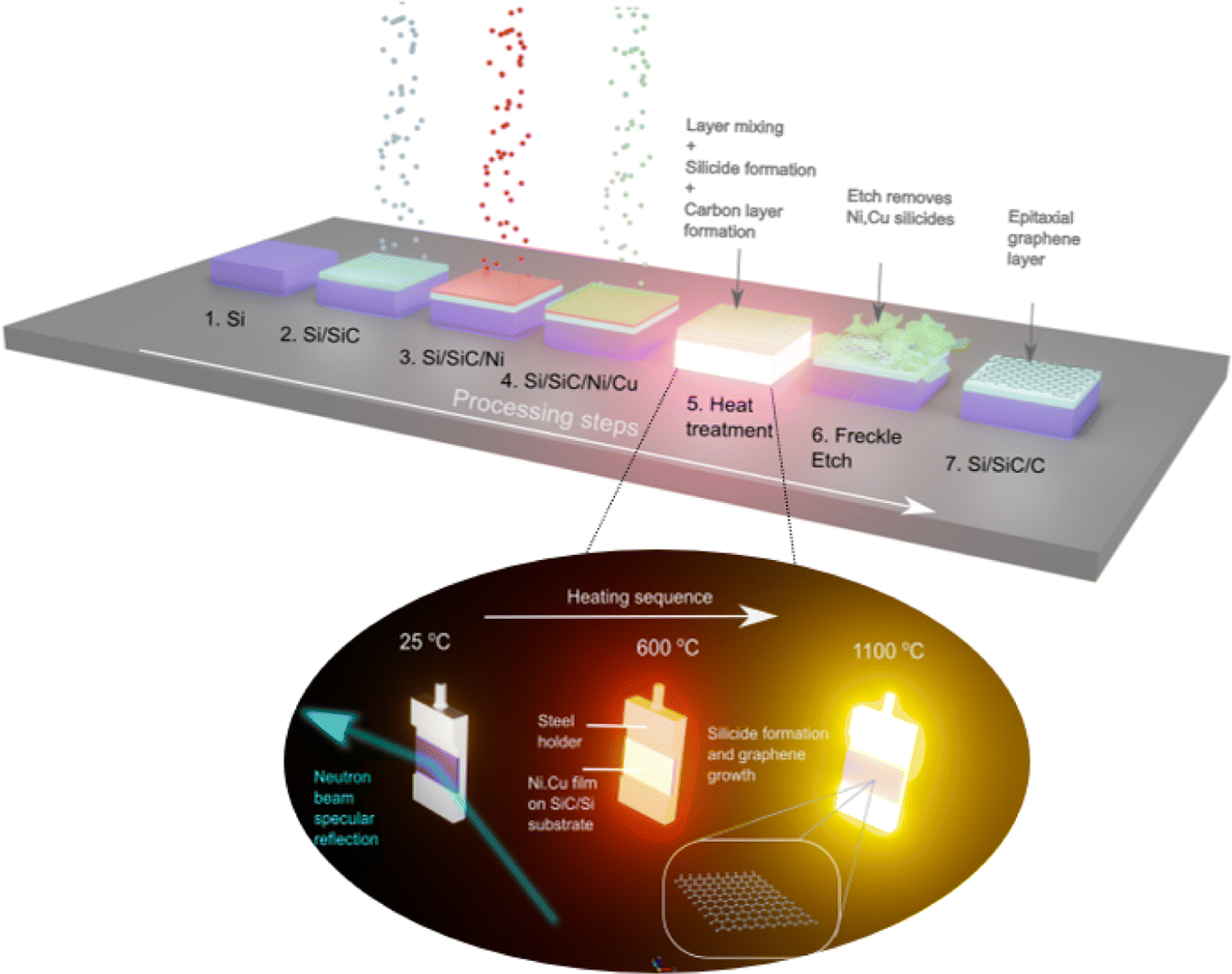 | ||
| Fig. 1 Schematic of the Ni/Cu catalytic alloy-mediated EG synthesis on 3C–SiC on silicon. | ||
2.2 Neutron reflectometry
In this work, we performed an in situ growth of EG on the 3C–SiC(100)/Si(100) and investigated the temperature-dependence of the alloy-mediated graphene layer formation using neutron reflectometry (NR). Variable temperature neutron reflectometry measurements were conducted in situ during a controlled annealing process on the Spatz time-of-flight neutron reflectometer at the 20 MW OPAL Multipurpose Reactor at the Australian Nuclear Science and Technology Organisation (ANSTO, Lucas Heights, Australia). The advantage of using neutrons for this application is that the neutron beam can penetrate through a vacuum furnace walls containing elements of niobium and aluminium to observe the conditions for graphene growth at 1100 °C. These types of measurements would be impossible with standard X-ray reflectometry (XRR) as X-rays cannot penetrate through the furnace's outer and inner walls. In addition, neutrons are advantageous for observing and differentiating lighter elements with similar mass such as carbon, oxygen and silicon, all involved in the graphene synthesis. This is related to their larger and distinct neutron scattering lengths.19 In contrast, X-ray scattering lengths for carbon, oxygen and silicon are relatively smaller and similar, making these elements less sensitive under X-rays, especially when higher atomic number elements like Ni and Cu are also present.22 Furthermore, neutrons also exhibit better contrast for Ni and Cu, whereas they are less distinct under X-rays.22Spatz is a time-of-flight reflectometer using cold neutrons with wavelengths from 2–20 Å, in a vertical scattering geometry as shown in Fig. 2.21 The data was reduced using the RefNX software package, and plotted in terms of the reduced scattering vector:
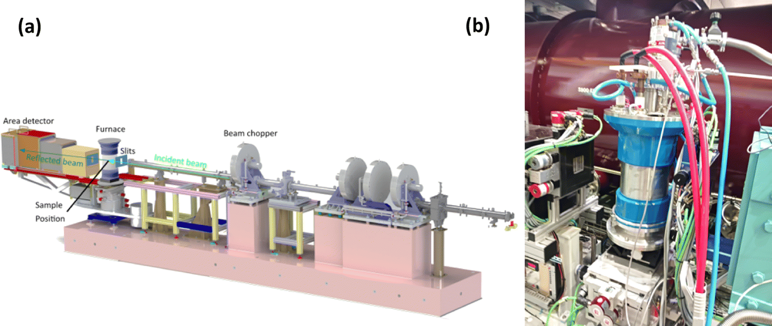 | ||
| Fig. 2 (a) The layout of the Spatz neutron beam instrument with furnace installed on the neutron beamline at the Australian Nuclear Science and Technology Organization (ANSTO), recreated from ref. 21 under creative commons licence CC BY 4.0 DEED. Green arrow indicates the neutron beam path. (b) Photograph of the furnace installed on the neutron beamline for EG synthesis and in situ monitoring using neutron reflectometry at ANSTO. | ||
2.3 X-ray reflectometry
Specular and off-specular X-ray reflectometry were performed using a Rigaku Smartlab II diffractometer where the X-ray wavelength was 1.5406 Å (Cu K-α). Specular data were fitted using the RefNX software. Modelling of the off-specular data used the BornAgain software25 deploying the Distorted Wave Born Approximation to model the Yoneda wings and correlated roughness.2.4 Raman spectroscopy
Room temperature (RT) Confocal Raman mapping was performed using a Renishaw InVia Raman spectrometer at 532 nm laser using a 100× objective with a spot size of ∼1 μm and incident power of 17 mW.12 Raman mapping was performed across an area of 30 μm × 30 μm at the center of the samples using a 0.2 μm step size and 0.1 s integration time. Raman intensity ratio maps of the D to G peak (ID/IG) and 2D to G peak (I2D/IG) are analyzed.2.5 Electrical characterization
Four-point InSn were soldered onto the EG/3C–SiC(100)/Si(100) annealed sample after wet freckle etching. Room temperature van-der Pauw Hall effect measurements were performed to measure the carrier type, carrier concentration, mobility and sheet resistance across a current range of 1–10 μA using an Ecopia Hall effect measurement system, HMS 5300 operating with a magnetic field of 0.55 T.3 Results and discussions
3.1 High temperature in operando neutron reflectometry
Fig. 3 shows the neutron reflectivity versus scattering vector, Q for different annealing temperatures starting from room temperature (RT) to 600 °C for the Cu/Ni/3C–SiC(100)/Si(100). The solid points are the data, and the solid lines are the corresponding fitting curves. Kiessig fringes are observed in Fig. 3 for the lower temperature data (<400 °C), which are related to the Ni and Cu layers with different SLDs. A slab model was used to fit the data with the top layer of Cu of thickness of 214.2 (±26.6) Å, SLD of 6.2 (±0.1) × 10−6 Å−2 and roughness of 11.8 (±5.0) Å, (see ESI Table S1† for fitted parameters).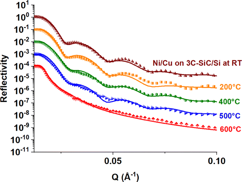 | ||
| Fig. 3 Neutron reflectivity experimental data obtained during the in situ annealing from room temperature to 600 °C of the thin Ni/Cu bilayer sputtered on 3C–SiC(100)/Si(100) for the growth of epitaxial graphene. Data are offset for clarity. Solid points represent the experimental data and solid lines represent the fitted curves. | ||
The Cu layer is followed by the Ni layer of thickness, SLD and roughness of 85.3 (±1.2) Å, 7.0 (±0.1) × 10−6 Å−2 and 1.6 (±2.2) Å, respectively. Whilst the copper layer matches expectation, the SLD value of the nickel layer is reduced by 15% from the value expected for fully dense nickel (mass density 7.9 g cm−3, SLD = 8.35 × 10⁻⁶ Å−2). This may reflect the nanocrystalline nature of the nickel layer which typically reduces the mass density by 10–20%, although some low-temperature interdiffusion with the copper may also contribute. The fitted SLD of the SiC substrate is 5.2 (±0.1) × 10−6 Å−2, matching the expected SLD based on the 3C crystal structure. The SiC has a roughness of 2.0 Å, determined in the neutron measurements. The SiC pseudosubstrate is sufficiently thick (∼500 nm) so that it appears as semi-infinite to the neutrons, and the underlying silicon layer is not detected, as the latter would yield an SLD of 2.01 × 10⁻⁶ Å−2 which is not detected experimentally. As temperature increases to 400 °C, the well-defined maxima and minima of the fringes gradually dampen, indicating the intermix of Ni and Cu layers and Ni–Cu alloy formation. The Kiessig fringes disappear at 600 °C. This is attributed to a sudden increase in surface/interface roughness, and also a loss of neutron scattering length density contrast as the surface layer SLD is decreased. Both phenomena indicate the start of a solid phase reaction, implying the onset of nickel silicides formation (NiSi2 in this case, as indicated in ref. 12), leading to silicon entering the surface region and reducing the SLD. This in turn implies the release of atomic carbon. The formation of NiSi2 at 600 °C is in good agreement with earlier reports in literature.26,27 Fig. 4 shows the corresponding SLD profiles versus distance for the fitted models from Fig. 3. The SLD profiles calculated for RT and 200 °C indicate the two distinct layers of Ni and Cu deposited on top of 3C–SiC for the EG synthesis. The data at 400 °C shows the alloy formation of Ni and Cu. Fig. 4 indicates that at 600 °C, the cupronickel layer and top SiC layers intermix to form nickel NiSi2. The 600 °C data indicates indeed a very diffuse, graded interface attributed to a diffusion profile of the silicon, copper and nickel related to a complex elemental concentration across the sample.
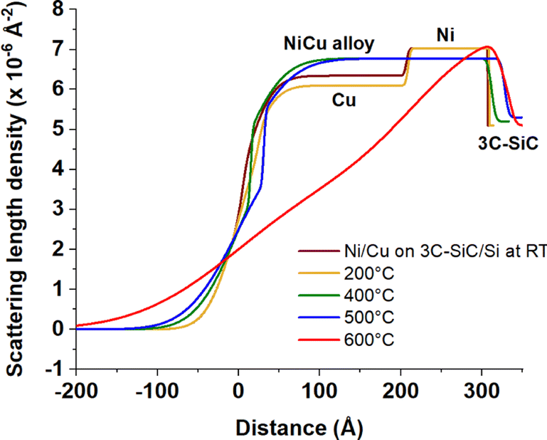 | ||
| Fig. 4 Calculated real-space SLD profiles corresponding to the data in Fig. 3. Note the Ni/Cu bilayer alloying above 200 °C and the high intermixing of the cupronickel alloy and the top of the SiC layer, indicating the start of formation of NiSi2, at 600 °C. | ||
After 1 hour of annealing at 1100 °C, data in Fig. 5 indicate the formation of a low-density surface layer with an SLD of 2.6 (±1.2) × 10−6 Å−2 (refer to Supplementary Table S2† for fitted values). This low-density layer can be related to the formation of a molten top layer at 1100 °C made of liquid nickel silicides/copper (melting points of NiSi2 and Cu are ∼993 °C and ∼1085 °C, respectively), supporting a liquid-phase epitaxial growth of EG.12,13 This growth condition can hence greatly benefit from a liquid-assisted diffusion18–20 during the carbon epitaxy. The data is fitted with a layer of carbon underneath the molten layer (see, Fig. 6) with thickness, SLD and roughness of 13.1 (±6.0) Å, 6.8 (±3.3) × 10−6 Å−2 and 7.7 (±5.3) Å respectively, indicating the graphene formation. Additionally, the data at 1100 °C could only be fitted with a silicate (Si–O–C) layer between the EG and the SiC, with thickness, SLD and roughness of 9.3 (±6.2) Å, 4.5 (±1.7) × 10−6 Å−2 and 5.2 (±3.1) Å, respectively (Supplementary Table S2†). This agrees with cross-sectional transmission electron microscopy (TEM) and time of flight secondary ion mass spectrometry (ToF-SIMS) depth profiling of graphene samples we reported in ref. 12, indicating the presence of graphene layer on top of a low-density silicate layer on the 3C–SiC.
 | ||
| Fig. 5 Neutron reflectivity experimental and fitted data obtained at 1100 °C and after the sample returned to RT – Markov chain Monte Carlo (MCMC) sampling data is shown in the supplementary. Dots represent the experimental data and solid lines represent the fit. The inset shows the reflectivity data and fit on the RQ4 scale for reflectivity over a limited Q range to highlight the differences between the two datasets. | ||
 | ||
| Fig. 6 SLD profiles for the fitted models for data at 1100C and after cooling to room temperature. MCMC sampling data is shown in the ESI, Fig. S1–S2.† | ||
The final RT measurement after cooling down shows a reduction of the thickness of the top-intermixed catalytic layer to 10.9 (±5.6) Å, from 34.0 (±24.2) Å at 1100 °C indicating a loss of metal by evaporation (primarily Cu, due to its appreciable volatility already from ∼400 °C28) during the high-temperature annealing. The loss of metallic elements during annealing is also evident from the decrease in total thickness of the metallic layers on top of the SiC from ∼300 (±27.8) Å before annealing to ∼10.9 (±5.6) Å after cooling back to RT, as shown in Table S1 and S2.† The RT data after cooling down, show the presence of a carbon (graphene) layer peak below the top/catalytic layer. The carbon layer representing the graphene was fitted with an SLD and roughness of 6.5 (±1.7) × 10−6 Å−2 and 10 (±4.8) Å, respectively. The silicate layer between the graphene and SiC was fitted with a thickness, SLD and roughness of 17.9 (±3.9) Å, 3.2 (±0.2) × 10−6 Å−2 and 1.3 (±1.8) Å, respectively.
MCMC sampling data for 1100 °C and RT is shown in the ESI Fig. S1–S2.† Although there is a large spread of fitted values for the graphene layer, this is to be expected given the featureless nature of the experimental data. However, note that it was not possible to fit the data adequately without adding the carbon (EG) and silicate layers. Additionally, as the thicknesses are comparable or smaller than layer roughness in several case, due to the diffuse and complex depth profile, the validity of the standard specular reflectometry calculation needs to be confirmed. In the ESI Fig. S3,† we present alternate calculations using micro-slicing of the SLD profile.
3.2 Ex-situ characterization
After the annealing step and in situ neutron measurements discussed earlier, the same samples were removed from the furnace and studied under ambient condition using X-ray and neutron reflectometry. Additional samples prepared on a standard laboratory furnace were also measured for comparison.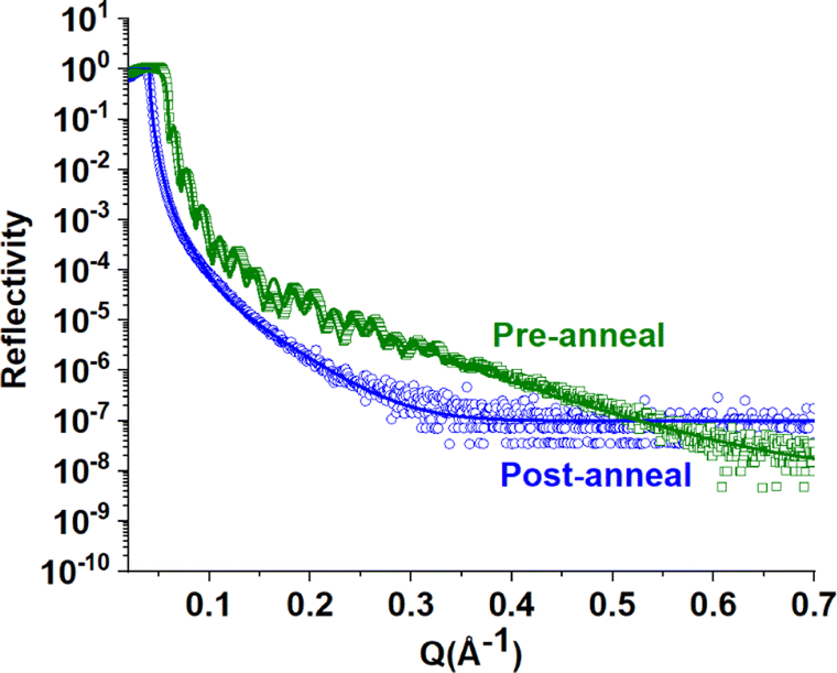 | ||
| Fig. 7 X-ray reflectivity of Ni/Cu sputtered 3C–SiC(100)/Si substrate before and after annealing, prior to etching. Solid lines indicate the fit. | ||
 | ||
| Fig. 8 SLD profiles for the fitted models for Ni/Cu sputtered 3C–SiC(100)/Si substrate before and after annealing, prior to etching. | ||
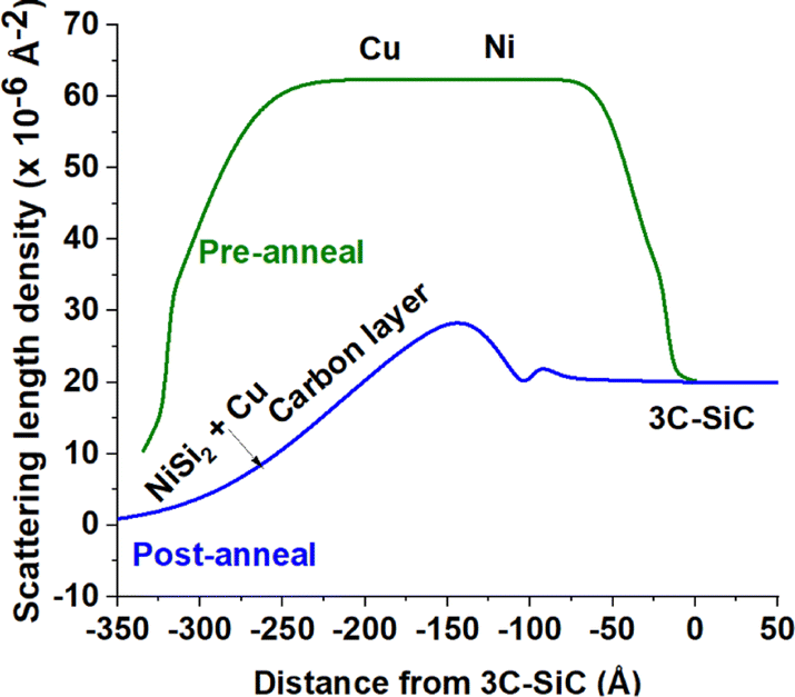
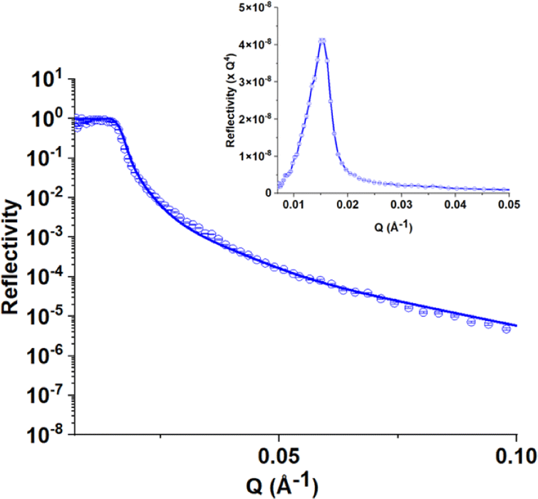
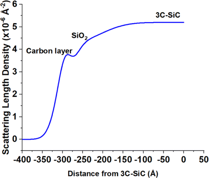
In addition to the samples used for neutron measurements, X-ray reflectometry measurements were performed on an EG film grown in a the standard Carbolite laboratory HT furnace used in ref. 14-see Fig. 9. Fig. 9a shows that the specular reflectivity of final epitaxial graphene (post-heating and etching) is different from the bare 3C–SiC/Si. These measurements can also be compared closely with the structural data for similar films in ref. 12 and reflectometry studies of graphene on 4H–SiC in ref. 6. The reflectivity intensity falls off more rapidly with the scattering vector (Q) in the EG samples compared to the 3C–SiC/Si samples. This implies that the surface roughness of graphene is larger than 3C–SiC/Si. We have previously reported that the root mean square roughness of alloy-mediated epitaxial graphene is about two-fold (∼9 nm) of the 3C–SiC/Si roughness (4 nm) as determined by atomic force microscopy.12 The X-ray and neutron roughness, which are both probes of the global average across the entire sample, are somewhat smaller, however display the same relative trend. There is also some indication of a single weak Kiessig fringe at – Q = 0.1 Å−1 in the EG samples, however it is heavily damped. Pristine, idealised graphene should yield well resolved fringes, albeit at higher Q. Previous work explained the observation of the damped fringe in SiC/EG as a result of the interlayer that forms between the graphene and SiC during the growth process.6 Here a simple two-layer model was used to fit the data as represented by the SLD profiles in Fig. 9b. The EG sample shows an additional thin layer. This is consistent with past reports6 (for example see, Fig. 5 of ref. 6) where it is attributed to a rough interface layer that forms between the EG and the SiC.
 | ||
| Fig. 9 (a) X-ray reflectivity of bare 3C–SiC(100)/Si(100) substrate and EG/3C–SiC(100) after freckle etching produced ex-situ (non-neutron). (b) SLD profile for the fitted model. The reflectivity intensity falls off more rapidly in the EG samples. This implies that the surface roughness of graphene is larger than 3C–SiC/Si. | ||
Through an off-specular XRR, we observed distinctive Yoneda scattering in the off-specular map, again implying that the surfaces of the films were rough, see Fig. 10. This yields a distinctive 3-peak rocking curve in the transverse scans. The observation of Yoneda scattering in SiC:C interfaces was reported previously in ref. 6 and the diffuse and off-specular scattering in our samples is remarkably similar. The origin of the scattering was proposed to arise from the SiC rough interface formed during the growth, however, has not been analysed quantitatively. To analyse the source of the scattering, calculations were performed in the Distorted Wave Born Approximation (DWBA). The model used a 29 Å roughness, and this roughness is primarily on the SiC surface, with a Hirst-factor of 0.1 and correlation length set to 3300 Å. The distinctive 2D map yields information on the correlation lengths in the bare SiC and EG coated SiC thin films. In particular, from the critical angle of the Yoneda scattering it is clear that the primary rough interface is at the SiC interface. If the graphene were thick enough or rough enough a second set of Yoneda wings should be observed. This finding confirmed by control measurements that revealed even blank SiC pseudosubstrate (even those without EG) yielded weak Yoneda scattering indicating the films are intrinsically rough. However, the nature of the 2D scattering was modified by the annealing process and EG formation, indicating additional roughness and disorder at EG/SiC interface. It is noted the Yoneda-wing patterns are comparable with the previous data for single crystal SiC:C interfaces6 suggesting that the alloy-mediated approach yields samples with comparable quality to the graphene obtained at higher temperature on monocrystalline SiC substrates.
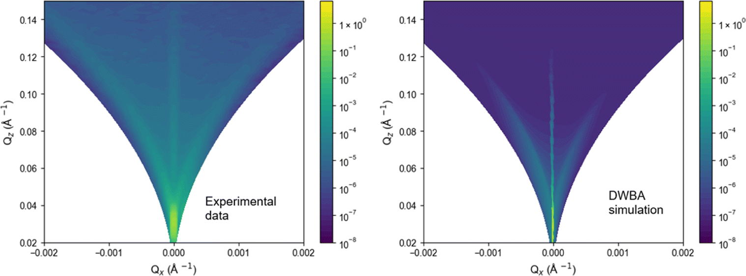 | ||
| Fig. 10 Off-specular X-ray reflectometry pattern of the SiC:C interface showing the distinctive Yoneda “angel” wing scattering leading to the “V” shaped intensity around the primary specular peak which is vertical at (Qx = 0). | ||
 | ||
| Fig. 11 Neutron reflectivity experimental and fitted data obtained for the annealed sample after wet freckle etching. The inset shows the reflectivity data and fit on the RQ4 scale for reflectivity over a limited Q range. | ||
 | ||
| Fig. 12 SLD profiles for the fitted models for data for the annealed sample after wet freckle etching. | ||
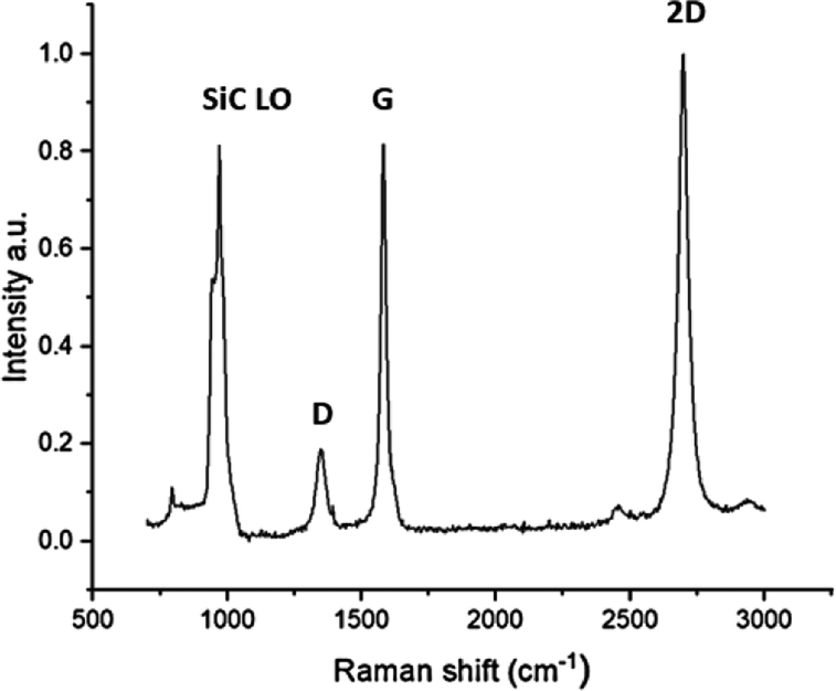 | ||
| Fig. 13 Raman averaged spectrum across a 30 × 30 μm2 area on the annealed sample after wet freckle etch. | ||
4 Conclusions
With a unique in operando (up to 1100 °C, below 5 × 10⁻⁵ mbar) neutron reflectometry setup and characterisation, this work gain insights into the epitaxial growth of graphene on 3C–SiC/Si using a thin bilayer of Ni/Cu as catalyst. The observations directly confirm that the metal silicide formation is a key ingredient enabling the release of atomic C from the SiC at relatively low temperatures to enable the formation of graphene. The operando observations also support the liquid-phase nature of the epitaxial growth occurring at 1100 °C, key to a uniform coverage of graphene despite of the very defective 3C–SiC template.Overall, the neutron reflectivity profiles sequentially illustrate all of the main steps and hallmarks of this epitaxial growth;
(a) Alloying of the Ni/Cu bilayer at 400 °C.
(b) Onset of nickel silicidation at 600 °C creating a highly intermixed layer on top of the 3C–SiC.
(c) Formation of a low-density, likely molten, catalyst layer around 1100 °C.
(d) Formation of a carbon (graphene) layer at 1100 °C, underneath the molten catalyst, and a thin silicate (Si–O–C) layer (SLD of 2.7 × 10⁻⁶ Å−2) in between the graphene and silicon carbide of thickness of ∼20 Å.
This work unlocks new avenues to use high temperature neutron reflectometry for the observation and optimization of wafer-scale growth of epitaxial graphene and other 2D materials for nanoelectronics and photonics.
Author contributions
The manuscript was written through the contributions of all authors.Conflicts of interest
There are no conflicts to declare.Acknowledgements
This research was partly supported by an AINSE Ltd. Early Career Researcher Grant (ECRG). This work was performed in part at the Australian Nuclear Science and Technology Organization. We thank ANSTO for providing neutron beamtime via proposal (14446). Spatz neutron beam operations are supported through the National Collaborative Research Infrastructure Strategy (NCRIS), an Australian Government initiative. We acknowledge Chris Baldwin and Michael Fenech for technical support at the Australian Centre for Neutron Scattering, ANSTO. AP and FI also acknowledge support by the ARC Centre of Excellence for Transformative Meta-Optical Systems (CE200100010).References
- C. Berger, Z. Song, T. Li, X. Li, A. Y. Ogbazghi, R. Feng, Z. Dai, A. N. Marchenkov, E. H. Conrad and P. N. First, Ultrathin epitaxial graphite: 2D electron gas properties and a route toward graphene-based nanoelectronics, J. Phys. Chem. B, 2004, 108, 19912–19916 CrossRef CAS.
- J. L. Tedesco, B. L. VanMil, R. L. Myers-Ward, J. M. McCrate, S. A. Kitt, P. M. Campbell, G. G. Jernigan, J. C. Culbertson, C. Eddy and D. K. Gaskill, Hall effect mobility of epitaxial graphene grown on silicon carbide, Appl. Phys. Lett., 2009, 95, 122102 CrossRef.
- Y.-M. Lin, C. Dimitrakopoulos, K. A. Jenkins, D. B. Farmer, H.-Y. Chiu, A. Grill and P. Avouris, 100-GHz transistors from wafer-scale epitaxial graphene, Science, 2010, 327, 662 CrossRef CAS PubMed.
- F. Speck, J. Jobst, F. Fromm, M. Ostler, D. Waldmann, M. Hundhausen, H. B. Weber and T. Seyller, The quasi-free-standing nature of graphene on H-saturated SiC (0001), Appl. Phys. Lett., 2011, 99, 122106 CrossRef.
- W. Norimatsu and M. Kusunoki, Structural features of epitaxial graphene on SiC {0 0 0 1} surfaces, J. Phys. D: Appl. Phys., 2014, 47, 094017 CrossRef CAS.
- A. Mazza, A. Miettinen, A. Daykin, X. He, T. Charlton, M. Conrad, S. Guha, Q. Lu, G. Bian and E. Conrad, Revealing interfacial disorder at the growth-front of thick many-layer epitaxial graphene on SiC: a complementary neutron and X-ray scattering investigation, Nanoscale, 2019, 11, 14434–14445 RSC.
- N. Mishra, J. Boeckl, N. Motta and F. Iacopi, Graphene growth on silicon carbide: A review, Phys. Status Solidi A, 2016, 213, 2277–2289 CrossRef CAS.
- A. Pradeepkumar, N. Mishra, A. R. Kermany, J. J. Boeckl, J. Hellerstedt, M. S. Fuhrer and F. Iacopi, Catastrophic degradation of the interface of epitaxial silicon carbide on silicon at high temperatures, Appl. Phys. Lett., 2016, 109, 011604 CrossRef.
- A. Pradeepkumar, M. Zielinski, M. Bosi, G. Verzellesi, D. K. Gaskill and F. Iacopi, Electrical leakage phenomenon in heteroepitaxial cubic silicon carbide on silicon, J. Appl. Phys., 2018, 123, 215103 CrossRef.
- A. Pradeepkumar, H. Cheng, K. Liu, M. Gebert, S. Bhattacharyya, M. Fuhrer and F. Iacopi, Low-leakage epitaxial graphene field-effect transistors on cubic silicon carbide on silicon, J. Appl. Phys., 2023, 133, 174503 CrossRef CAS.
- A. Pradeepkumar, D. K. Gaskill and F. Iacopi, Electronic and transport properties of epitaxial graphene on SiC and 3C-SiC/Si: a review, Appl. Sci., 2020, 10, 4350 CrossRef CAS.
- N. Mishra, J. J. Boeckl, A. Tadich, R. T. Jones, P. J. Pigram, M. Edmonds, M. S. Fuhrer, B. M. Nichols and F. Iacopi, Solid source growth of graphene with Ni–Cu catalysts: towards high quality in situ graphene on silicon, J. Phys. D Appl. Phys., 2017, 50, 095302 CrossRef.
- F. Iacopi, N. Mishra, B. V. Cunning, D. Goding, S. Dimitrijev, R. Brock, R. H. Dauskardt, B. Wood and J. Boeckl, A catalytic alloy approach for graphene on epitaxial SiC on silicon wafers, J. Mater. Res., 2015, 30, 609 CrossRef CAS.
- A. Pradeepkumar, M. Amjadipour, N. Mishra, C. Liu, M. S. Fuhrer, A. Bendavid, F. Isa, M. Zielinski, H. Sirikumara, T. D. K. G. Jayasekera and F. Iacopi, p-type Epitaxial Graphene on Cubic Silicon Carbide on Silicon for Integrated Silicon Technologies, ACS Appl. Nano Mater., 2019, 830–841 Search PubMed.
- B. V. Cunning, M. Ahmed, N. Mishra, A. R. Kermany, B. Wood and F. Iacopi, Graphitized silicon carbide microbeams: wafer-level, self-aligned graphene on silicon wafers, Nanotechnol., 2014, 25, 325301 CrossRef PubMed.
- D. A. Katzmarek, A. Mancini, S. A. Maier and F. Iacopi, Direct synthesis of nanopatterned epitaxial graphene on silicon carbide, Nanotechnol, 2023, 34, 405302 CrossRef PubMed.
- M. Suemitsu and H. Fukidome, Epitaxial graphene on silicon substrates, J. Phys. D Appl. Phys., 2010, 43, 374012 CrossRef.
- M. Jankowski, M. Saedi, F. La Porta, A. C. Manikas, C. Tsakonas, J. S. Cingolani, M. Andersen, M. de Voogd, G. J. van Baarle and K. Reuter, Real-time multiscale monitoring and tailoring of graphene growth on liquid copper, ACS Nano, 2021, 15, 9638–9648 CrossRef CAS PubMed.
- S. Zheng, M. Zeng, H. Cao, T. Zhang, X. Gao, Y. Xiao and L. Fu, Insight into the rapid growth of graphene single crystals on liquid metal via chemical vapor deposition, Sci. China Mater., 2019, 62, 1087–1095 CrossRef CAS.
- M. Mauk, P. Sims, J. Rand and A. Barnett, in Practical Handbook of Photovoltaics: Fundamentals and Applications, ed. T. Markvart, Elsevier, USA, 2nd edn, 2012, ch. 4, pp. 161–206 Search PubMed.
- A. P. Le Brun, T.-Y. Huang, S. Pullen, A. R. Nelson, J. Spedding and S. A. Holt, Spatz: the time-of-flight neutron reflectometer with vertical sample geometry at the OPAL research reactor, J. Appl. Crystallogr., 2023, 56, 18–25 CrossRef CAS PubMed.
- Y. Ren and X. Zuo, Synchrotron X-ray and neutron diffraction, total scattering, and small-angle scattering techniques for rechargeable battery research, Small Methods, 2018, 2, 1800064 CrossRef.
- A. R. Nelson and S. W. Prescott, refnx: neutron and X-ray reflectometry analysis in Python, J. Appl. Crystallogr., 2019, 52, 193–200 CrossRef CAS PubMed.
- A. R. McCluskey, A. J. Caruana, C. J. Kinane, A. J. Armstrong, T. Arnold, J. F. Cooper, D. L. Cortie, A. V. Hughes, J.-F. Moulin and A. R. Nelson, Advice on describing Bayesian analysis of neutron and X-ray reflectometry, J. Appl. Crystallogr., 2023, 56, 12–17 CrossRef CAS PubMed.
- G. Pospelov, W. Van Herck, J. Burle, J. M. Carmona Loaiza, C. Durniak, J. M. Fisher, M. Ganeva, D. Yurov and J. Wuttke, BornAgain: software for simulating and fitting grazing-incidence small-angle scattering, J. Appl. Crystallogr., 2020, 53, 262–276 CrossRef CAS PubMed.
- P. Poulopoulos, A. Goschew, S. Pappas, V. Karoutsos, A. Straub, P. Fumagalli, M. Velgakis, W. Schommers and C. Politis, Graphene-Assisted Growth of Nanoblocks of Single-Crystalline Epitaxial Nickel Disilicides on Si (001), J. Surf., 2014, 2, 161–165 Search PubMed.
- A. M. Thron, P. K. Greene, K. Liu and K. van Benthem, Structural changes during the reaction of Ni thin films with (1 0 0) silicon substrates, Acta Mater., 2012, 60, 2668–2678 CrossRef CAS.
- G. W. C. Kaye and D. Ewen, The sublimation of metals at low pressures, Proc. R. Soc. A, 1913, 89, 58–67 Search PubMed.
- E. Rollings, G.-H. Gweon, S. Zhou, B. Mun, J. McChesney, B. Hussain, A. Fedorov, P. First, W. De Heer and A. Lanzara, Synthesis and characterization of atomically thin graphite films on a silicon carbide substrate, J. Phys. Chem. Solids, 2006, 67, 2172–2177 CrossRef CAS.
- C. Li, X. Li, W. Yu, R. Xiao, F. Huang, H. Tian, C. Wang, X. Chen and J. Shao, Scalable fabrication of turbostratic graphene with high density and high ion conductivity for compact capacitive energy storage, Matter, 2023, 6, 4032–4049 CrossRef CAS.
Footnote |
| † Electronic supplementary information (ESI) available. See DOI: https://doi.org/10.1039/d3ra08289j |
| This journal is © The Royal Society of Chemistry 2024 |