
 Open Access Article
 This Open Access Article is licensed under a Creative Commons Attribution-Non Commercial 3.0 Unported Licence
Spike rate dependent synaptic characteristics in lamellar, multilayered alpha-MoO3 based two-terminal devices – efficient way to control the synaptic amplification†
Meenu Maria Sunny ab and
R. Thamankar*b
ab and
R. Thamankar*b
aDepartment of Physics, Vellore Institute of Technology, Vellore, TN, India. E-mail: meenumaria.sunny2020@vitstudent.ac.in
bCentre for Functional Materials, Vellore Institute of Technology, Vellore, TN, India. E-mail: rameshm.thamankar@vit.ac.in
First published on 15th January 2024
Abstract
Brain-inspired computing systems require a rich variety of neuromorphic devices using multi-functional materials operating at room temperature. Artificial synapses which can be operated using optical and electrical stimuli are in high demand. In this regard, layered materials have attracted a lot of attention due to their tunable energy gap and exotic properties. In the current study, we report the growth of layered MoO3 using the chemical vapor deposition (CVD) technique. MoO3 has an energy gap of 3.22 eV and grows with a large aspect ratio, as seen through optical and scanning electron microscopy. We used transmission electron microscopy (TEM) and X-ray photoelectron spectroscopy for complete characterisation. The two-terminal devices using platinum (Pt/MoO3/Pt) exhibit superior memory with the high-resistance state (HRS) and low-resistance state (LRS) differing by a large resistance (∼MΩ). The devices also show excellent synaptic characteristics. Both optical and electrical pulses can be utilised to stimulate the synapse. Consistent learning (potentiation) and forgetting (depression) curves are measured. Transition from long term depression to long term potentiation can be achieved using the spike frequency dependent pulsing scheme. We have found that the amplification of postsynaptic current can be tuned using such frequency dependent spikes. This will help us to design neuromorphic devices with the required synaptic amplification.
Computation beyond von Neumann architecture is becoming more and more attractive in the era of big data and the internet of things. Brain inspired architecture is a way forward to achieve highly efficient, low power consuming computing systems. This can be done by means of in-sensor computing, spiking neural network (SNN) and artificial intelligence (AI).1–8 The advent of AI and big data brings in challenges to the computing hardware and systems. Conventional von Neumann computing systems have the processor and memory in different physical locations limiting the processing speed, particularly when dealing with big data which consumes a lot of power, and it is also limited by the data transfer between the memory and processor (the von Neumann bottleneck) thus limiting the computing capability of these platforms.9,10 In order to process such big data, the existing hardware architecture following Moore’s law poses serious challenges in embedding more and more memory and processors in a given area or volume. In this sense, computing architectures designed with new ideas and new materials are very much essential for highly efficient systems consuming lesser power. Thinking of designing the very high density architecture, inspiration can be taken from the human brain. The human brain contains around 1011 neurons connected with 1015 synapses, and can perform complex computation with an extremely small power consumption of 1–10 fJ per event.9,11–13 Our brain does this in a smart way by distributing the work into different places in the brain. It is well established that neuron–synapse form the fundamental pair in brain-inspired computation.14 As the action potential is reached at the presynaptic region, the neuron transmits the information via synapses. This way, it consumes extremely low power of ∼20 W. Synapses are the units where the amplification and depression of the signal occur resulting in the learning and forgetting effect in the human brain. The strength of connection between two neurons, called the synaptic weight, can be optimized. Emulating the biological neuron–synapse–neuron activity in solid state devices is at the heart of the design of bio-inspired computational devices and systems. In an ideal scenario, Si-based neuromorphic devices and systems are required to make them compatible to the already existing Si-based complementary metal–oxide–semiconductor (CMOS) devices. Since the conventional Si-based device miniaturization has reached a bottleneck, new materials and device manufacturing are needed for high-density, highly-efficient devices and systems.15–17
Memristors or resistive switching memory devices are one of the device architectures which have attracted a lot of attention recently. These are simply, two terminal devices which store information in the form of different resistance states. These devices have shown long memory retention, non-volatile switching and high data density.18 Interestingly, the resistive switching devices are compatible for substituting the existing complementary metal–oxide–semiconductor (CMOS) based memory technology. A basic memristive device has two metal electrodes and an insulating layer sandwiched between them (M–I–M structure). The device can switch between a high-resistance state and a low-resistance state by the application of voltage.20–22 The switching materials used in the devices vary from thin films,23 low dimensional materials,24 and organic materials.25,26 There are also reports on carbon dots, hydrogen-bonded organic frameworks and graphene oxide based memristive devices.27–29 Among the most commonly used switching materials, metal oxide based switching devices have fascinated the scientific world due to the low power consumption, fast switching and low operating voltages. Transition Metal Oxides (TMOs) belong to the category of materials beyond graphene and, among them, TiO2,30,31 WO3,32 VO2,33,34 STO,35–37 ZnO38 and HfO239 have been used as active materials exhibiting reversible resistive switching behaviour for non-volatile memory (NVM) device applications. In these switching devices, the information is stored between a high-resistance state (HRS) and a low-resistance state (LRS). The switching mechanism in a device is explained mainly based on the charge conduction behaviour in a fabricated device such as ohmic conduction, trap assisted charge conduction techniques, thermionic emission, and hopping conduction methods. Usually, the current–voltage characteristics in an LRS state are mostly ohmic.40 Molybdenum oxide (MoO3) is a transition metal oxide which can be grown easily in two dimensions. The electrical properties of such low dimensional MoOx can be tuned by controlling the stoichiometry.18 It has been confirmed that two dimensional MoOx grows in two stable forms namely MoO2 and MoO3. MoO2 grows in a distorted rutile-like monoclinic structure while MoO3 grows as orthorhombic structure. Interestingly, MoO3 grows in the form of a layered, large band gap semiconductor.19,20 The properties of intermediate structures for MoO3−x can be tuned by controlling the oxygen vacancies. Lamellar MoO3 can grow even in ambient conditions by heating molybdenum metal in oxygen ambient conditions.41,42 More controlled stoichiometry of MoO3 is achieved by growing in a chemical vapour deposition (CVD) chamber by controlling the oxygen partial pressure. Recently, large area growth of α-MoO3 has been achieved using the CVD technique and successfully tested for optoelectronic applications.43,44 Two-dimensional MoO3 layers have been used as a high-κ dielectric to fabricate a Ni/WSe2 based transistor where the MoO3 will inject holes into the WSe2 channel layer.45 This study is focused on the utilisation of CVD grown lamellar MoO3 multilayered sheets as switching materials and incorporating them as an active part of a synapse that mimics basic functionalities of the biological synapse. In order to ensure the uniform distribution of nanosheets for device fabrication, the prepared multilayers are ultrasonicated for more than two hours in ethanol.
We use as fabricated Pt electrodes (schematic is shown in Fig. 1c) (Micrux technologies, SPAIN). Detailed information about the electrodes used is given in Fig. S1 (see the ESI†). The electrode system contains 150 pairs of Pt/Ti electrodes on a glass substrate within a circular region spanning a diameter of 3 mm. Initially 50 nm thick titanium is used as a bottom layer which acts as a wetting layer and then 150 nm thick platinum electrodes create 150 pairs of electrodes separated by 5 μm. The pre-patterned electrodes are cleaned using ethanol, acetone and distilled water alternatively and dried. Finally, well-characterised MoO3 multilayers which are uniformly distributed in ethanol are drop-casted into these electrodes and annealed at 150 °C for 2 hours. The electrical measurements are performed at room temperature using a Keysight B2902B source meter, including both dc–voltage sweep and pulsed voltage measurements.
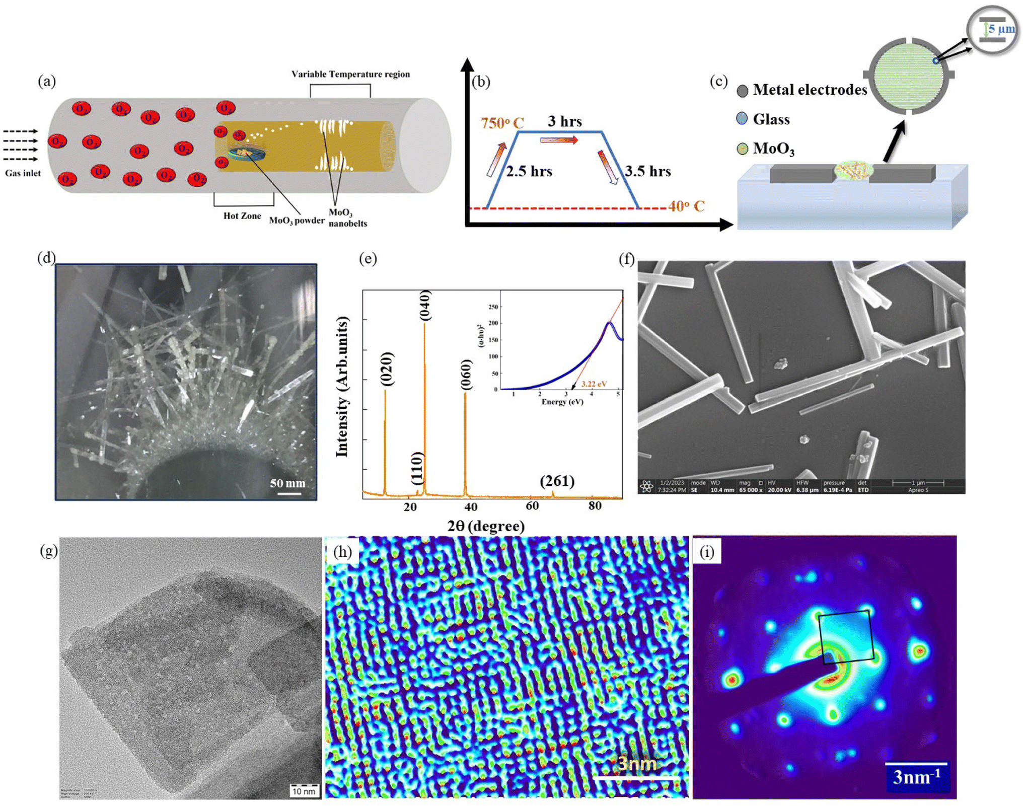 | ||
| Fig. 1 (a) Schematic diagram of the CVD furnace used for preparation of the MoO3 nanosheets. The growth of nanosheets is done in the presence of oxygen partial pressure. Various temperature zones are indicated. (b) The typical temperature sequence employed during the synthesis of layered MoO3. (c) The two-terminal device configuration where prefabricated Pt electrodes are used. The inter-electrode gap is 5 μm. (d) Photograph showing the typical growth of few centimeter long layered MoO3 around the quartz tube at the hot–cold zone interface. These nanosheets are collected carefully from the CVD furnace. (e) The X-ray diffraction pattern of the layered MoO3. The typical XRD pattern indicates growth along the [010] direction indicated by strongest peaks at 2θ ∼ 12.3°, 22.9° and 38.5°. Inset shows the Tauc plot used for calculation of the energy gap ∼3.22 eV. (f) Individual lamellar MoO3 with large aspect ratio are seen in the high resolution scanning electron image. (g–i) Results of transmission electron microscopy of MoO3. The high resolution TEM images show the MoO3 lattice growing along the (10) and (01) directions. The Fourier transform of the topography image clearly indicates bright spots along the (10) and (01) directions indicating the growth directions. | ||
1 Results and discussion
Lamellar MoO3 sheets were synthesised using the Chemical Vapor Deposition technique (CVD) where, MoO3 powder was used as the precursor (see Fig. 1a and b). 3 g of MoO3 powder was taken in a quartz crucible and kept inside the hot zone region of the CVD tube under an oxygen atmosphere of 100 sccm flow for 3 h at 750 °C and 2 millibar pressure. We obtained lamellar MoO3 with sizes ranging from a few millimeters to centimeters in length (Fig. 1d) and this was carefully collected from the cold zone of the CVD tube after the chamber was cooled to room temperature. A few milligrams of as-synthesised material was sonicated for a duration of two hours in ethanol. The product obtained was then cleaned and washed with ethanol using centrifugation (1000 rpm/5 min), where the residue was separated from the supernatant and dried. The final product was preserved in a glass vial for further characterisation and device fabrication. Before investigating the electrical properties and checking the synaptic properties, it is necessary to establish the crystallographic phase of the layered MoO3 prepared. Two of the most commonly known phases of MoO3 are α-MoO3 and the metastable β-MoO3.19,46,47 As reported, a spontaneous phase transition between β → α occurs in the temperature range of 375–400 °C.48 The interesting phase of MoO3 is the α-phase, so we kept the CVD chamber temperature well above the phase transition temperature so that the product phase is completely the α-phase and ruling out any possibility of mixed phase formation. A typical XRD-pattern obtained for the large multilayered MoO3 samples is shown in Fig. 1e. The strongest diffraction peaks are found at 2θ values of 12.3°, 22.9° and 38.5° corresponding to the (020), (040) and (060) crystallographic planes, respectively. As shown in Fig. 1f, the layered MoO3 grow with very high aspect ratio which is essential for our purpose. The UV-vis spectroscopy done on such layered MoO3 shows that the energy gap is ∼3.22 eV as shown using the Tauc plot (inset Fig. 1e).49 Transmission electron microscopy images shown in Fig. 1g–i reveal that the MoO3 grow in the form of sheets and atomically resolved images suggest that layers grow along [01] and [10] showing orthorhombic MoO3 sheets. The Fourier transform of the topography image clearly indicates the bright spots along [01] and [10] clearly indicating the growth of orthorhombic MoO3 sheets. A detailed calculation of the lattice fringes is shown in ESI Fig. S1.† From the average distance between the spots along the (10) and (01) directions, we find that the real lattice dimensions are 0.276 nm along the (10) direction and 0.274 nm along the (01) direction. A detailed analysis of the TEM images is shown in Fig. S1 in the ESI.† To determine the chemical composition and the chemical states of the MoO3 surfaces, X-ray photoelectron spectroscopy (XPS) was performed over the lamellar layers and is shown in Fig. 2. The survey scan shows the characteristics peaks of molybdenum (Mo), oxygen (O), trace amounts of carbon (C) and then the O-KLL Auger peaks. A high resolution scan was conducted in order to determine the valence band edge of the MoO3 sample (inset Fig. 2a). The valence band edge is found to be at 2.79 eV (x-intercept of the red line scan of increasing intensity). The overall intensity at this low energy scan can be fitted with multiple peaks located at 4.68 eV, 6.47 eV and 8.56 eV respectively. The broad intensity observed in the energy range between 1 eV to 6 eV is due to metallic Mo coming from Mo-4d and Mo-5s orbitals,.50,52 while O-2p orbital contribution is observed between 4 eV to 10 eV indicating there is a strong overlap between the Mo-4d and O-2p orbitals in the MoO3 as expected in the pure α-MoO3. It is to be noted that we do not see the doublet near to the Fermi energy which is associated with the presence of MoO2 phase in the sample.50 High resolution narrow scans are done at the binding energy range of the Mo-3d core level and oxygen-1s core levels to identify the chemical states of the elements (Fig. 2b and c respectively). Well-resolved Mo-3d5/2 and Mo-3d3/2 levels due to spin–orbit splitting occur at 232.58 eV and 235.68 eV respectively. These are doublet states of molybdenum in the Mo6+ state. The energy gap between Mo-3d5/2 and Mo-3d3/2 levels is 3.1 eV and the areas under the curve are in the ratio of 3![[thin space (1/6-em)]](https://www.rsc.org/images/entities/char_2009.gif) :2 indicating clearly that the MoO3 has molybdenum in the Mo6+ oxidation state. We do not see the corresponding peak for Mo5+ occurring at lower binding energies as seen in the literature.51 A clear peak at 530.48 eV shown in Fig. 2c is due to the O2− ions present in the MoO3 layers. The binding energy peak at 530.48 eV of oxygen clearly confirms lattice oxygen rather than oxygen defects. If we consider the small shoulder at 532.68 eV of the oxygen peak, which is coming from the nonlattice oxygen, the concentration of such nonlattice oxygen content is about 9.45% which we consider as very low. This is due to the higher partial pressure of oxygen we have used during the growth of MoO3 wherein oxygen vacancies are compensated most efficiently. We do not observe any adsorbed water molecules on the MoO3 layer which would show up as OH–MoO3 resulting in the reduction of MoO3 to MoO2.51 The peak at 284.52 eV shown in Fig. 2d corresponding to the C-1s peak is from the standard for the corrections to the data obtained from the XPS (adventitious carbon peaks (AdC)). We can also observe the C–O and C
:2 indicating clearly that the MoO3 has molybdenum in the Mo6+ oxidation state. We do not see the corresponding peak for Mo5+ occurring at lower binding energies as seen in the literature.51 A clear peak at 530.48 eV shown in Fig. 2c is due to the O2− ions present in the MoO3 layers. The binding energy peak at 530.48 eV of oxygen clearly confirms lattice oxygen rather than oxygen defects. If we consider the small shoulder at 532.68 eV of the oxygen peak, which is coming from the nonlattice oxygen, the concentration of such nonlattice oxygen content is about 9.45% which we consider as very low. This is due to the higher partial pressure of oxygen we have used during the growth of MoO3 wherein oxygen vacancies are compensated most efficiently. We do not observe any adsorbed water molecules on the MoO3 layer which would show up as OH–MoO3 resulting in the reduction of MoO3 to MoO2.51 The peak at 284.52 eV shown in Fig. 2d corresponding to the C-1s peak is from the standard for the corrections to the data obtained from the XPS (adventitious carbon peaks (AdC)). We can also observe the C–O and C![[double bond, length as m-dash]](https://www.rsc.org/images/entities/char_e001.gif) O bonds completely coming from the adventitious carbon present during the investigation. From the XPS spectrum, we can infer that our CVD grown MoO3 layers are close to MoO3 stoichiometry with the possibility of having a small oxygen deficiency.52
O bonds completely coming from the adventitious carbon present during the investigation. From the XPS spectrum, we can infer that our CVD grown MoO3 layers are close to MoO3 stoichiometry with the possibility of having a small oxygen deficiency.52
 | ||
| Fig. 2 Detailed XPS analysis of layered MoO3: (a) survey scan of MoO3. The inset shows the detailed scan of the valence band edge. The line fit shows that the valence band edge is 2.79 eV from the Fermi level. Multipeak fitting reveals the presence of peaks at 4.68 eV, 6.47 eV and 8.56 eV which can be assigned to metallic Mo (4d and 5s) orbitals, O-2s orbitals with strong overlapping of Mo-4d and O-2s orbitals. (b) High resolution binding energy scan of Mo-3d orbitals. (c) High resolution binding energy scan of O-1s orbitals. (d) Adventitious carbon peaks (AdC) reveal the energy levels of single bonds and double bonds between carbon and oxygen atoms. | ||
2 Conduction mechanism and memory devices
The uniformly dispersed MoO3 multilayers are dropcast onto the prefabricated electrodes and the devices are post-annealed at 150 °C for a few hours to remove all the solvent from the devices. Typical nonlinear current–voltage characteristics can be seen for Pt/MoO3/Pt as shown in Fig. 3a. The device operates at very low current (few nA), which is very much essential for our purpose, and can be attributed to the highly compensated MoO3 lattice. Even though abrupt resistive switching is not seen in our devices as seen in vertical devices, the analog switching shown by our devices can be used for multi-state operation. Here one should note that the hysteresis is still very small but consistently observed in the devices. In the case of the Pt/MoO3/Pt device, there is an asymmetry in the current–voltage characteristics. To understand the conduction mechanism, the current–voltage characteristics are fitted according to conduction mechanisms occurring at various voltage regimes. For the fitting of the HRS state (Fig. 3b), a linear relation between ln(I) vs. V0.5 is obtained between the bias range from 0.5 V to 2.22 V. The corresponding slope of the curve is 2.26 indicating the Schottky emission in the HRS state. In the case of the LRS state (Fig. 3c), a linear relation between ln(I) vs. ln(V) with s = 1.2 confirms ohmic conduction. We adopted pulsed voltage measurements to check the applicability of our devices to memory applications. Standard read–write–erase–read pulses (WRITE at 4 V, READ at 1 V and ERASE at −3.5 V). As indicated in Fig. 3d, clear ON/OFF states can be obtained for the chosen pulse voltage. The device shows excellent stability with respect to the high-resistance state (HRS) and low-resistance state (LRS) within the ∼nA range. The stability of HRS/LRS states have been tested for up to 1000 cycles as indicated in Fig. 3e and the states show excellent stability with HRS/LRS differing by ∼0.68 nA. Since the device works in the low current regime, we tested our device performance for still lower WRITE and ERASE pulses as indicated in Fig. 3f so that we could operate it in a lower current range. As shown in Fig. 3f, very stable HRS and LRS states can be maintained over 1000 cycles with HRS–LRS states separated by only ∼0.25 nA. For lower operating voltages, say ∓3 V, the device also shows very stable HRS and LRS states with current differing by 0.19 nA as shown in Fig. S2.† It is very important to note that the devices show a stable WRITE/ERASE operation at lower current levels which are very important for all practical purposes when using layered materials.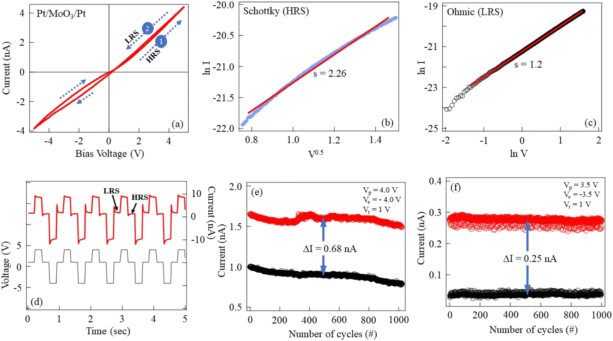 | ||
| Fig. 3 (a–c) show current–voltage characteristics of Pt/MoO3/Pt based devices. (a) Typical nonlinear I–V curve with very small hysteresis shown by device. (b) In the high-resistance state, the conduction is due to Schottky emission as indicated by linear ln(I) vs. V0.5 relation. (c) The linear relation between ln(I) vs. ln(V) shows that there is ohmic conduction in the low-resistance state. (d–f) show the results of read–write–erase–read measurements. (d) A few cycles of the READ–WRITE–READ–ERASE cycles used for measurements. The HRS/LRS state is indicated. (e) For a WRITE voltage of 4 V, the stability of HRS/LRS states are tested for 1000 cycles. The read voltage used here is 1 V. (f) Stable HRS and LRS can be seen for the Vp = ∓3.5 V retained for 1000 cycles. | ||
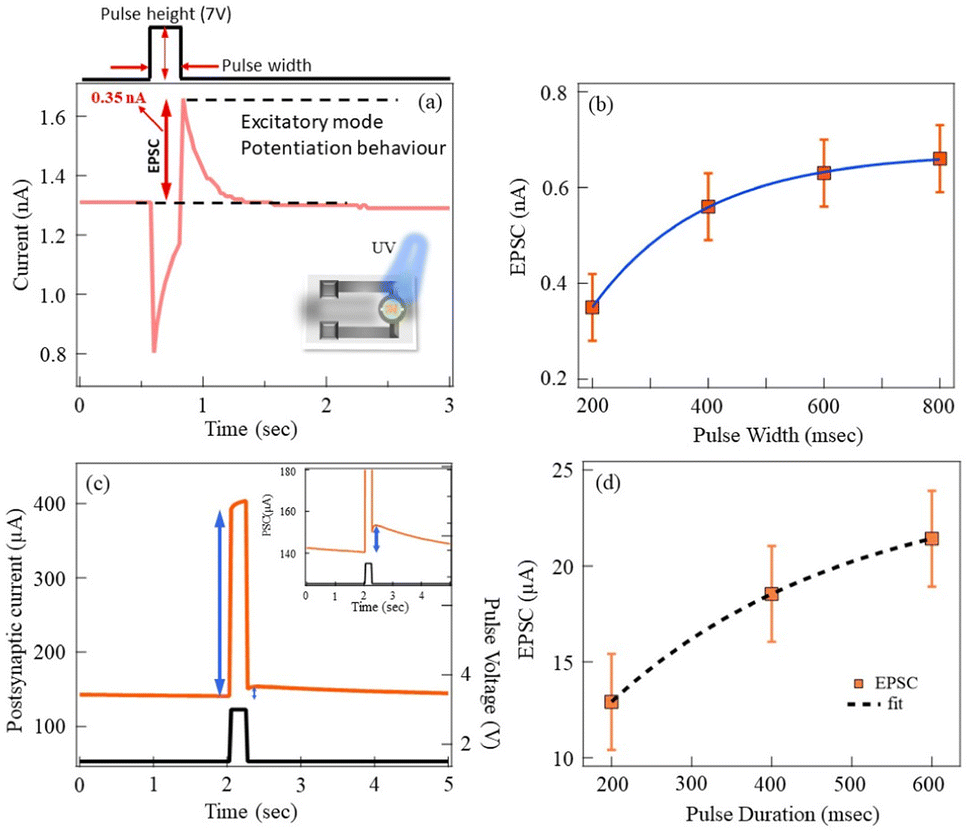
In a biological synapse, the information is transferred from the presynaptic neuron to postsynaptic neuron via a biological synapse. Information transmission occurs via the synapse when a voltage stimulus is injected into the presynaptic neuron. The synapse modulates this signal and the postsynaptic neuron receives the signal. Similarly, here we apply a voltage pulse to the electrode 1 which acts as a presynaptic neuron and the postsynaptic current is monitored at electrode 2 (see Fig. S1† for the correct identification of electrode 1 and electrode 2). We have found that our lamellar α-MoO3 has an optical energy gap of 3.22 eV from the UV-vis measurements. Therefore a UV-LED of 375 nm is selected for the optical excitation of the synaptic device. The excitatory postsynaptic current (EPSC) generated from our MoO3 device is shown in Fig. 4a. A pulse voltage (7 V/200 ms) was applied to the UV-LED and EPSC was detected. At the end of the voltage pulse, the EPSC reached a maximum value EPSCmax = 1.66 nA and then decayed slowly and returned to the initial value within 1 s. This can be attributed to the short term memory in the device due to the optical pulse. Similarly the optical synaptic excitation is created by using a voltage pulse as shown in Fig. 4c. In this case also, EPSC is observed when a positive (3 V/200 ms) pulse was applied to the left electrode. EPSC again decays slowly taking a longer time to attain the initial pre-pulse value (more than 5 s). We have performed such measurements using both optical and electrical pulses with various pulse widths and the EPSC has been plotted as a function of pulse width. The results are shown in Fig. 4b and d. An exponential increase in the EPSC is seen in both cases with characteristic time constants τoptical ∼ 192 s and τelectrical ∼ 303 s. Any synaptic device fabricated must be checked for the frequency dependent synaptic weight update. Because individual device can show long-term potentiation and long-term depression depending on the spike frequencies. Here, we use the terms “spike” and “excitatory postsynaptic current (EPSC)” for depicting the voltage pulse and the measured transient current after the pulse respectively, to express the emulation of biological synaptical activity. The frequency dependent plasticity (FDP) is a specific feature of memristive devices where the synaptic weight update depends on the frequency of applied voltage pulses.53–56 This behaviour is modelled using the Bienenstock–Cooper–Munro (BCM) learning rule.57–59 and explains the onset of long-term potentiation (LTP) and long-term depression (LTD). Long-term potentiation and long-term depression can be stimulated in a memristive device by modifying the spike frequencies. The devices are stimulated by a given number of voltage pulses at various frequencies and the postsynaptic current is measured with respect to time. We applied 15 voltage pulses of fixed pulse voltage Vp = ±3 V and varied the frequency from 1 Hz to 16 Hz. Fig. 5a show the results of such measurements for Pt/MoO3/Pt. It is clear that for the spike frequency of 1 Hz, the EPSC gradually reduces, indicating a long-term depression (LTD). The EPSC reduced from 0.609 mA to 0.478 mA for the Pt/MoO3/Pt device. As the spike frequency increased to 2 Hz, we observed an enhancement in the EPSC. Further increase in the spike frequency resulted in a clear increase in the EPSC, indicating that the device exhibits long-term potentiation (LTP). This change can be explained by considering the temporal effect of pulses on the post-synaptic current. The temporal effect increases as the applied spike frequency increased which clearly mimics the biological synapse where the diffusive Ca2+ ion concentration determines the short-term plasticity. One such demonstration of controlled short-term plasticity was shown in an SiOxNy:Ag memristor. Here, controlled diffusion of Ag+ ion from the Ag clusters has been attributed to the short-term plasticity. Applied electric field would enhance the diffusion of the Ag+ ions and relaxing to original current level when the applied field is taken out. The diffusive dynamics of the Ag+ ions could generate a transition from LTD to LTP and again LTD in such memristors.60 We have performed such controlled change from LTD to LTP with spike frequency. We attribute the phenomenon to the regulated creation of oxygen vacancies in the layered MoO3 contributing to enhanced conduction giving rise to LTP and then relaxation when the pulse voltage is absent. Similar spike frequency dependence of the post-synaptic current has been reported in various memristive devices. Especially when the spike rate-dependent plasticity (SRDP) increases with the spike frequency, the devices can be used for high-pass filters applications.61,62
 | ||
| Fig. 4 Excitatory postsynaptic current induced by both optical pulse and electrical pulse. (a) An optical pulse of wavelength 375 nm/200 ms applied to the device. (b) Effect of optical pulse width on the EPSC signal. (c) The EPSC obtained in the device using 3 V electrical pulse. Inset shows clear LTP characteristics. (d) Effect of electrical pulse width on the EPSC signal. | ||
 | ||
| Fig. 5 Frequency dependent EPSC measurements. (a) Frequency dependent EPSC measured for Pt/MoO3/Pt device. Fifteen voltage pulses are applied at various frequencies. The inset shows the EPSC when the device is triggered at 10 Hz. (b) The ratio of PSC for the 15th and first pulse. Yellow shaded region shows the EPSC from no-gain to 100% gain. (c and d) Transition from a short-term depression to long-term depression can be seen by operating the device at different spike frequency. At lower frequency (1 Hz), the PSC decays to the initial state within a few seconds while for the device operated at 16 Hz, the PSC is retained for more than 20 s. | ||
For clarity, we show the EPSC measured for a spike frequency of 10 Hz for Pt/MoO3/Pt in the inset of Fig. 5a where A1 and A15 are the amplitude of measured EPSC for the first pulse and fifteenth pulse respectively. The PSC after the first voltage pulse denoted as A1 is 0.365 mA and the synaptic current amplitude for A15 is 0.446 mA. We calculate the synaptic gain as ratio A15/A1 of the Pt/MoO3/Pt device. As shown in Fig. 5b, the synaptic gain is almost constant for the various spike frequencies used in our investigation. This might be due to the fact that the first 15 pulses will already create a potentiation which will later saturate for a further increase in the number of pulses. To check if the EPSC increases with the frequency for smaller number of pulses, we chose 10 pulses and repeated the experiment for different frequencies. As seen in Fig. 5b, the EPSC shows a marked different trend compared to the larger number of pulses. The EPSC increases linearly with the frequency of the spikes. This kind of pulse frequency dependence is termed as spike rate-dependent plasticity (SRDP). From our results, it is established that SRDP can be achieved for various frequencies with a smaller number of pulses. For the chosen 10 pulses, SRDP increases by 20% as the frequency of voltage pulses increased from 1 Hz to 16 Hz.63 It is interesting to note that there exists a cut-off frequency (fcutoff) below which the (A10/A1) is less than 100% indicating LTD at lower frequencies. If the spike frequency is above this cutoff, then we will get EPSC amplification. The change in the EPSC from STM to LTM can be understood by considering the spike dependent activation of oxygen vacancies. When the spike frequency is too low, a fewer number of oxygen vacancies can be activated and be driven to the other electrode. This results in reduced EPSC and is considered as LTD. When higher spike frequency used, then more and more oxygen vacancies are activated thus giving rise to enhancement of the EPSC resulting in LTM. In psychology, there are two synaptic plasticities discussed often namely short-term memory (STM) and long-term memory (LTM). In particular STM lasts for a very short period of time due to weak potentiation while LTM persists for more hours due to strong potentiation. By changing the frequency, the STP-to-LTP transition or the other way has been measured in many cases. In the case of Pt/MoO3/Pt devices, we have observed long-term potentiation when the applied spike frequencies increase. In the Pt/MoO3/Pt device, apart from the SRDP gain, we also found that there is a transition from STP to LTP as spike frequency is varied from 1 Hz to 16 Hz frequency. As shown in Fig. 5c, for spike frequency 1 Hz, we find that the PSC returns back to its pre-spike value within 2 s. When the spike frequency is 16 Hz, the PSC is retained for more than 20 s as shown in Fig. 5d. This can be considered as LTP and we have shown a transition from STP to LTP. In general, for the lower spike frequency case, after each spike, enough time is available for the PSC to decay to the original level or close to the original level. This implies that applying multiple pulses has negligible effect on the cumulative PSC. This also gives rise to STP after the pulse train is applied. When the spike frequency is higher, between each voltage spike there is not enough time for the PSC to decay before the next pulse arrives. Thus the accumulation of post-synaptic current will also be higher for a given number of voltage spikes. At the end of the pulse train, we see a higher PSC (indicated by the blue dotted line in Fig. 5b). Generally such transition from STP to LTP is observed in the optical synapses. We are successful in getting this transition in the electronic synapse. It is noteworthy that the spike stimulation adopted here from frequency dependent plasticity results in the synaptic weight update precisely matching with the biological synapse. This suggests that the synaptic weight update is highly dependent on the presynaptic spiking rate and thus the reiterative spike voltages with higher frequencies will lead to higher synaptic weight.
3 Emulating the biological synapse
After understanding the MoO3 and the conduction mechanism in such devices, we tested the suitability of the devices for neuromorphic applications. Fig. 6a and b show schematic diagrams of the similarity between the biological synapse and an artificial synapse. Our devices based on MoO3 will act as an artificial synapse. In the case of the biological synapse, the signal transmission takes place via synaptic connections once an action potential approaches the neuron–synapse junction. When the signal approaches the synapse from the pre-synaptic neuron, neurotransmitters are released through the synapse and a post-synaptic signal (PSC) is generated in the second neuron. During the transmission through the synapse, the signal will be either amplified or compressed. This modulation of the signals is called the synaptic weight which results in the learning and forgetting processes in the biological synapse. A similar performance is replicated in the solid state devices by applying constant potential pulses with a given pulse width while the current is monitored with respect to time which forms the post-synaptic current. Depending on the polarity of the pulse voltages applied, it is possible to get the learning and forgetting characteristics in the devices. In the case of Pt–MoO3, we apply a series of negative pulses for potentiation and positive voltages for depression. The action potentials occurring in the biological synapses are replicated by carefully choosing the pulse voltage amplitude for the potentiation and depression. Fig. 6c shows one cycle of the potentiation and depression curve for the Pt/MoO3/Pt device with pulse amplitude Vp = 3 V and pulse time 200 ms. We applied 40 pulses for potentiation and depression in all the cases. The enhancement of the post-synaptic current (PSC) can be seen for negative pulse voltages. For the positive pulses, the PSC reduces with the number of voltage pulses resulting in a forgetting curve. The enhancement and reduction of the post-synaptic current typically resembles the learning (LTP) curve and forgetting (LTD) curve in the biological synapse. If one carefully observes the post-synaptic current, there is a slow reduction in the current level after each potentiation cycle. This effect can be attributed to the incomplete SET process for the number of pulses we have used. This effectively reduces the current level at the end of the following depression cycle. This might effectively give a smaller post-synaptic current at the end of each cycle. Further, if one takes the absolute change within a given cycle, the overall change is within the measurement limits (1 to 2 × 10⁻¹⁰ shown in Fig. S4b).†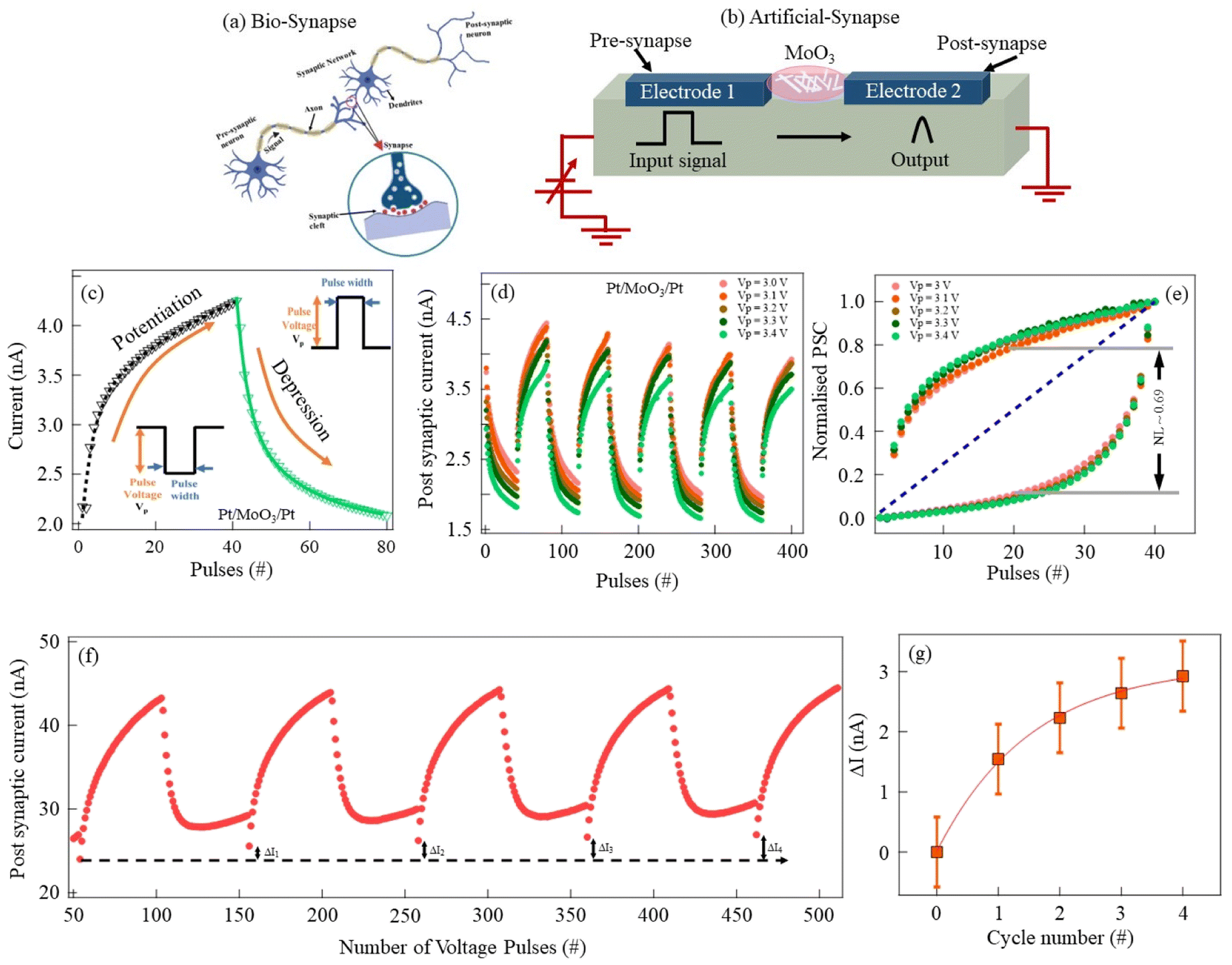 | ||
| Fig. 6 (a) Schematic diagram of biological synapse. (b) The artificial synapse using the two-terminal devices based on layered MoO3. We used prefabricated Pt electrodes. (c) Single cycle of potentiation and depression curve for Pt/MoO3/Pt device. The continuous curve is fitted using a double exponential as shown in eqn (1). A pulse of amplitude 3 V with pulse width 200 ms was used. (d) Series of potentiation and depression curves measured to check the stability of the device. (e) The non-linearity calculated for the Pt/MoO3/Pt devices. 20th pulse is used to quantify the nonlinearity. (f) Potentiation and depression curves for continuously varying pulse voltage pulses. Progressively, the memory retention can be improved by repeated learning–forgetting operation as indicated by ΔI after each cycle. (g) The evolution of ΔI with each cycle of potentiation and depression. | ||
In all our measurements, we see the synaptic weight update showing nonlinear behaviour. It follows a double exponential given by
|
PSC = I0 + A0exp[−(x − x0)/t1] + A1exp[−(x − x0)/t2]
| (1) |
To check the reliability of the potentiation and depression, we performed the measurements for multiple cycles with multiple pulse voltages. Fig. 6d displays the results of such measurements which show consistent learning and forgetting curves. Again, the negative voltage pulses are used for potentiation (learning) and positive pulses are used for depression (forgetting) curves. The potentiation and depression follow eqn (1) for all the cycles. Interestingly, the total synaptic weight update (ΔI) for individual pulse voltage remains almost independent of pulse voltage used as shown in Fig. S2 in the ESI.† This also indicates that various pulse voltages used with the ideal pulse sequence do not cause appreciable change in the learning and forgetting curves. The potentiation and depression always show a nonlinear update as shown in Fig. 6e. We calculated the nonlinearity (NL) factor as a parameter that quantifies the device quality. We used the 20th pulse as a reference for the NL factor calculation. For the Pt/MoO3/Pt device, our measurements show that the nonlinearity factor is ∼0.69 and the calculated nonlinear factor for various pulse voltages used changes within the error margin. This means an ideal series of pulse voltages would not help the device to show a linear learning (potentiation) and forgetting (depression).
Memory retention for a long time is an essential characteristic of the human brain. This is very important when multiple learning (potentiation)–forgetting (depression)–relearning operations are done. We applied a non-ideal pulse sequence to the device and monitored the PSC for many cycles. We increased the pulse voltage from 1.6 V to 3.6 V in steps of 40 mV per step. As shown in Fig. 6f, multiple cycles of operation resulted in an enhanced memory indicated by ΔI. The gradual increase in the retention is indicated by the double sided arrow after each cycle (Fig. 6f). As the device is subjected to multiple cycles of potentiation and depression, the memory retention also increases. The growth of memory retention in such a case follows
|
PSC = I0 + A0exp[−x/τ]
| (2) |
4 Conclusions
In summary, we fabricated multilayered, low dimensional MoO3 based artificial synaptic devices using pre-fabricated Pt electrodes separated by 5 μm. The initial characterisation shows that the CVD-prepared α-MoO3 are grown in a lamellar structure evidenced by high resolution transmission electron microscopy images. We observe excellent synaptic characteristics, including consistent potentiation and depression curves lasting multiple cycles. The potentiation and depression curves follow a double exponential growth. The excitatory post-synaptic current (EPSC) depends on the spike rate and we find that the device can show transition from short-term memory to long-term memory depending on the spike rate applied. By repeated learning–forgetting–learning operations, the memory retention can be improved. Our studies on lamellar MoO3 can pave the way to design and fabricate the high performing artificial synaptic devices. By fine tuning the spike frequency of operation, we can achieve 100% enhancement in memory which is essential in designing optimally operating neuromorphic devices in future computing applications.Conflicts of interest
The authors declare that they have no competing financial interests or personal relationships that could have appeared to influence the work reported in this paper.Acknowledgements
The authors would like to thank the Centre for Functional Materials, Vellore Institute of Technology, for their support during this research work. The authors would like to acknowledge Dr Ramakrishnan Ganesan, BITS Pilani Hyderabad Campus, for his technical help during the scanning electron microscopy (SEM) and X-ray photoelectron spectroscopy (XPS) measurements. The authors would like to acknowledge SCIF, SRMIST for providing the instrumentation facilities such as the transmission electron microscope for the sample analysis. MMS acknowledges the Department of Science and Technology (DST), India, for providing the graduate student fellowship Inspire Fellowship under DST/Inspire fellowship/2020/IF200272. The authors acknowledge Dr Ankur Rastogi, Centre for Functional Materials (CFM), VIT Vellore, for technical suggestions and critical reading of the manuscript.Notes and references
- W. Zhang, B. Gao, J. Tang, P. Yao, S. Yu, M.-F. Chang, H.-J. Yoo, H. Qian and H. Wu, Neuro-inspired computing chips, Nat. Electron., 2020, 3(7), 371 CrossRef.
- T. Hasegawa, K. Terabe, T. Tsuruoka and M. Aono, Atomic Switch: Atom/Ion Movement Controlled Devices for Beyond Von-Neumann Computers, Adv. Mater., 2012, 24(2), 252 CrossRef CAS PubMed.
- M. A. Zidan, J. P. Strachan and W. D. Lu, The future of electronics based on memristive systems, Nat. Electron., 2018, 1(1), 22 CrossRef.
- J.-Q. Yang, R. Wang, Y. Ren, J.-Y. Mao, Z.-P. Wang, Y. Zhou and S.-T. Han, Neuromorphic Engineering: From Biological to Spike-Based Hardware Nervous Systems, Adv. Mater., 2020, 32(52), 2003610 CrossRef.
- Y. Kang, Y. Chen, Y. Tan, H. Hao, C. Li, X. Xie, W. Hua and T. Jiang, Bioinspired activation of silent synapses in layered materials for extensible neuromorphic computing, J. Mater., 2023, 9(4), 787 Search PubMed.
- Z. Wu, P. Shi, R. Xing, Y. Xing, Y. Ge, L. Wei, D. Wang, L. Zhao, S. Yan and Y. Chen, Quasi-two-dimensional α-molybdenum oxide thin film prepared by magnetron sputtering for neuromorphic computing, RSC Adv., 2022, 12(28), 17706–17714 RSC.
- T. Guo, B. Sun, S. Ranjan, Y. Jiao, L. Wei, Y. N. Zhou and Y. A. Wu, From Memristive Materials to Neural Networks, ACS Appl. Mater. Interfaces, 2020, 12(49), 54243–54265 CrossRef CAS PubMed.
- S. K. Acharya, E. Galli, J. B. Mallinson, S. K. Bose, F. Wagner, Z. E. Heywood, P. J. Bones, M. D. Arnold and S. A. Brown, Stochastic Spiking Behavior in Neuromorphic Networks Enables True Random Number Generation, ACS Appl. Mater. Interfaces, 2021, 13(44), 52861–52870 CrossRef CAS PubMed.
- J. Bian, Z. Cao and P. Zhou, Neuromorphic computing: devices, hardware, and system application facilitated by two-dimensional materials, Appl. Phys. Rev., 2021, 8(4), 041313 CAS.
- S. Goswami, S. Goswami and T. Venkatesan, An organic approach to low energy memory and brain inspired electronics, Appl. Phys. Rev., 2020, 7(2), 021303 CAS.
- G. Lee, J.-H. Baek, F. Ren, S. J. Pearton, G.-H. Lee and J. Kim, Artificial Neuron and Synapse Devices Based on 2D Materials, Small, 2021, 17(20), 2100640 CrossRef CAS.
- S. Herculano-Houzel, The remarkable, yet not extraordinary, human brain as a scaled-up primate brain and its associated cost, Proc. Natl. Acad. Sci. U. S. A., 2012, 109, 10661–10668 CrossRef CAS.
- J.-K. Han, J. Oh, G.-J. Yun, D. Yoo, M.-S. Kim, J.-M. Yu, S.-Y. Choi and Y.-K. Choi, Cointegration of single-transistor neurons and synapses by nanoscale CMOS fabrication for highly scalable neuromorphic hardware, Sci. Adv., 2021, 7(32), eabg8836 CrossRef CAS PubMed.
- C. Frenkel, D. Bol and G. Indiveri, Bottom-Up and Top-Down Approaches for the Design of Neuromorphic Processing Systems: Tradeoffs and Synergies Between Natural and Artificial Intelligence, Proc. IEEE, 2023, 111(6), 623–652 CAS.
- Y. Tuchman, T. N. Mangoma, P. Gkoupidenis, Y. van de Burgt, R. A. John, N. Mathews, S. E. Shaheen, R. Daly, G. G. Malliaras and A. Salleo, Organic neuromorphic devices: past, present, and future challenges, MRS Bull., 2020, 45(8), 619–630 CrossRef.
- D. Marković, A. Mizrahi, D. Querlioz and J. Grollier, Physics for neuromorphic computing, Nat. Rev. Phys., 2020, 2(9), 499–510 CrossRef.
- V. K. Sangwan and M. C. Hersam, Neuromorphic nanoelectronic materials, Nat. Nanotechnol., 2020, 15(7), 517–528 CrossRef CAS.
- F. Rahman, T. Ahmed, S. Walia, E. Mayes, S. Sriram, M. Bhaskaran and S. Balendhran, Reversible resistive switching behaviour in CVD grown, large area MoOx, Nanoscale, 2018, 10(42), 19711 RSC.
- K. Kalantar-zadeh, J. Tang, M. Wang, K. L. Wang, A. Shailos, K. Galatsis, R. Kojima, V. Strong, A. Lech, W. Wlodarski and R. B. Kaner, Synthesis of nanometre-thick MoO3 sheets, Nanoscale, 2010, 2(3), 429–433 RSC.
- R. Waser, R. Dittmann, G. Staikov and K. Szot, Redox-Based Resistive Switching Memories – Nanoionic Mechanisms, Prospects, and Challenges, Adv. Mater., 2009, 21(25–26), 2632–2663 CrossRef CAS PubMed.
- K. Zhu, M. R. Mahmoodi, Z. Fahimi, Y. Xiao, T. Wang, K. Bukvišová, M. Kolíbal, J. B. Roldan, D. Perez, F. Aguirre and M. Lanza, Memristors with Initial Low-Resistive State for Efficient Neuromorphic Systems, Adv. Intell. Syst., 2022, 4, 2200001 CrossRef.
- G. Milano, M. Aono, L. Boarino, U. Celano, T. Hasegawa, M. Kozicki, S. Majumdar, M. Menghini, E. Miranda, C. Ricciardi, S. Tappertzhofen, K. Terabe and I. Valov, Quantum Conductance in Memristive Devices: Fundamentals, Developments, and Applications, Adv. Mater., 2022, 34, 2201248 CrossRef CAS.
- E. Carlos, R. Branquinho, R. Martins, A. Kiazadeh and E. Fortunato, Recent Progress in Solution-Based Metal Oxide Resistive Switching Devices, Adv. Mater., 2021, 33(7), 2004328 CrossRef CAS.
- C. S. Yang, D. S. Shang, N. Liu, G. Shi, X. Shen, R. C. Yu, Y. Q. Li and Y. Sun, A Synaptic Transistor based on Quasi-2D Molybdenum Oxide, Adv. Mater., 2017, 29(27), 1700906 CrossRef.
- L. Yuan, S. Liu, W. Chen, F. Fan and G. Liu, Organic Memory and Memristors: From Mechanisms, Materials to Devices, Adv. Electron. Mater., 2021, 7(11), 2100432 CrossRef CAS.
- T. Zeng, Z. Yang, J. Liang, Y. Lin, Y. Cheng, X. Hu, X. Zhao, Z. Wang, H. Xu and Y. Liu, Flexible and transparent memristive synapse based on polyvinylpyrrolidone/N-doped carbon quantum dot nanocomposites for neuromorphic computing, Nanoscale Adv., 2021, 3(9), 2623–2631 RSC.
- C. Zhang, Y. Li, F. Yu, G. Wang, K. Wang, C. Ma, X. Yang, Y. Zhou and Q. Zhang, Visual growth of nano-HOFs for low-power memristive spiking neuromorphic system, Nano Energy, 2023, 109, 108274 CrossRef CAS.
- C. Zhang, M. Chen, Y. Pan, Y. Li, K. Wang, J. Yuan, Y. Sun and Q. Zhang, Carbon Nanodots Memristor: An Emerging Candidate toward Artificial Biosynapse and Human Sensory Perception System, Adv. Sci., 2023, 10(16), 2207229 CrossRef CAS.
- Y. Li, S. Ling, R. He, C. Zhang, Y. Dong, C. Ma, Y. Jiang, J. Gao, J. He and Q. Zhang, A robust graphene oxide memristor enabled by organic pyridinium intercalation for artificial biosynapse application, Nano Res., 2023, 16(8), 11278 CrossRef CAS.
- K. Szot, M. Rogala, W. Speier, Z. Klusek, A. Besmehn and R. Waser, TiO2—a prototypical memristive material, Nanotechnology, 2011, 22(25), 254001 CrossRef CAS PubMed.
- R. Miyake, Z. Nagata, K. Adachi, Y. Hayashi, T. Tohei and A. Sakai, Versatile Functionality of Four-Terminal TiO2−x Memristive Devices as Artificial Synapses for Neuromorphic Computing, ACS Appl. Electron. Mater., 2022, 4(5), 2326 CrossRef CAS.
- X. He, Y. Yin, J. Guo, H. Yuan, Y. Peng, Y. Zhou, D. Zhao, K. Hai, W. Zhou and D. Tang, Memristive properties of hexagonal WO3 nanowires induced by oxygen vacancy migration, Nanoscale Res. Lett., 2013, 8(1), 50 CrossRef.
- A. Rana, C. Li, G. Koster and H. Hilgenkamp, Resistive switching studies in VO2 thin films, Sci. Rep., 2020, 10(1), 3293 CrossRef CAS.
- J. del Valle, J. G. Ramírez, M. J. Rozenberg and I. K. Schuller, Challenges in materials and devices for resistive-switching-based neuromorphic computing, J. Appl. Phys., 2018, 124(21), 211101 CrossRef.
- H. Nili, T. Ahmed, S. Walia, R. Ramanathan, A. E. Kandjani, S. Rubanov, J. Kim, O. Kavehei, V. Bansal, M. Bhaskaran and S. Sriram, Microstructure and dynamics of vacancy-induced nanofilamentary switching network in donor doped SrTiO3−x memristors, Nanotechnology, 2016, 27(50), 505210 CrossRef.
- H. J. H. Ma and J. F. Scott, Non-Ohmic Variable-Range Hopping and Resistive Switching in SrTiO3 Domain Walls, Phys. Rev. Lett., 2020, 124(14), 146601 CrossRef CAS PubMed.
- T. Ahmed, S. Walia, J. Kim, H. Nili, R. Ramanathan, E. L. H. Mayes, D. W. M. Lau, O. Kavehei, V. Bansal, M. Bhaskaran and S. Sriram, Transparent amorphous strontium titanate resistive memories with transient photoresponse, Nanoscale, 2017, 9(38), 14690 RSC.
- U. B. Isyaku, M. H. B. M. Khir, I. M. Nawi, M. A. Zakariya and F. Zahoor, ZnO Based Resistive Random Access Memory Device: A Prospective Multifunctional Next-Generation Memory, IEEE Access, 2021, 9, 105012–105047 Search PubMed.
- Y. Wang, G. Zhou, B. Sun, W. Wang, J. Li, S. Duan and Q. Song, Ag/HfOx/Pt Unipolar Memristor for High-Efficiency Logic Operation, J. Phys. Chem. Lett., 2022, 13(34), 8019–8025 CrossRef CAS.
- M. H. Alam, S. Chowdhury, A. Roy, X. Wu, R. Ge, M. A. Rodder, J. Chen, Y. Lu, C. Stern, L. Houben, R. Chrostowski, S. R. Burlison, S. J. Yang, M. I. Serna, A. Dodabalapur, F. Mangolini, D. Naveh, J. C. Lee, S. K. Banerjee, J. H. Warner and D. Akinwande, Wafer-Scalable Single-Layer Amorphous Molybdenum Trioxide, ACS Nano, 2022, 16(3), 3756–3767 CrossRef CAS PubMed.
- K. Kalantar-zadeh, J. Tang, M. Wang, K. L. Wang, A. Shailos, K. Galatsis, R. Kojima, V. Strong, A. Lech, W. Wlodarski and R. B. Kaner, Synthesis of nanometre-thick MoO3 sheets, Nanoscale, 2010, 2(3), 429–433 RSC.
- J. Lu, C. Sun, M. Zheng, Y. Wang, M. Nripan, J. A. van Kan, S. G. Mhaisalkar and C. H. Sow, Ultrasensitive Phototransistor Based on K-Enriched MoO3 Single Nanowires, J. Phys. Chem. C, 2012, 116(41), 22015–22020 CrossRef CAS.
- A. Arash, T. Ahmed, A. Govind Rajan, S. Walia, F. Rahman, A. Mazumder, R. Ramanathan, S. Sriram, M. Bhaskaran, E. Mayes, M. S. Strano and S. Balendhran, Large area synthesis of 2D MoO3−x for enhanced optoelectronic applications, 2D Mater., 2019, 6(3), 035031 CrossRef CAS.
- B. Zheng, Z. Wang, Y. Chen, W. Zhang and X. Li, Centimeter-sized 2D α-MoO3−x single crystal: growth, Raman anisotropy, and optoelectronic properties, 2D Mater., 2018, 5(4), 045011 CrossRef CAS.
- B. A. Holler, K. Crowley, M.-H. Berger and X. P. A. Gao, 2D Semiconductor Transistors with Van der Waals Oxide MoO3 as Integrated High-κ Gate Dielectric, Adv. Electron. Mater., 2020, 6(10), 2000635 CrossRef CAS.
- R. L. Smith and G. S. Rohrer, Scanning Probe Microscopy of Cleaved Molybdates: α-MoO3(010), Mo18O52(100), Mo8O23(010), and η-Mo4O11(100), J. Solid State Chem., 1996, 124(1), 104–115 CrossRef CAS.
- P. F. Carcia and E. M. McCarron, Synthesis and properties of thin film polymorphs of molybdenum trioxide, Thin Solid Films, 1987, 155(1), 53–63 CrossRef CAS.
- W. M. R. Divigalpitiya, R. F. Frindt and S. R. Morrison, Oriented films of molybdenum trioxide, Thin Solid Films, 1990, 188(1), 173–179 CrossRef CAS.
- S. Balendhran, J. Deng, J. Z. Ou, S. Walia, J. Scott, J. Tang, K. L. Wang, M. R. Field, S. Russo, S. Zhuiykov, M. S. Strano, N. Medhekar, S. Sriram, M. Bhaskaran and K. Kalantar-zadeh, Enhanced Charge Carrier Mobility in Two-Dimensional High Dielectric Molybdenum Oxide, Adv. Mater., 2013, 25(1), 109–114 CrossRef CAS.
- K. P. Reddy, N. B. Mhamane, M. K. Ghosalya and C. S. Gopinath, Mapping Valence Band and Interface Electronic Structure Changes during the Oxidation of Mo to MoO3 via MoO2 and MoO3 Reduction to MoO2: A NAPPES Study, J. Phys. Chem. C, 2018, 122(40), 23034–23044 CrossRef CAS.
- A. R. Head, C. Gattinoni, L. Trotochaud, Y. Yu, O. Karslıoğlu, S. Pletincx, B. Eichhorn and H. Bluhm, Water (Non-)Interaction with MoO3, J. Phys. Chem. C, 2019, 123(27), 16836–16842 CrossRef CAS.
- X. Hou, J. Huang, M. Liu, X. Li, Z. Hu, Z. Feng, M. Zhang and J. Luo, Single-Crystal MoO3 Micrometer and Millimeter Belts Prepared from Discarded Molybdenum Disilicide Heating Elements, Sci. Rep., 2018, 8(1), 16771 CrossRef PubMed.
- J. Wen, L. Q. Zhu, Y. M. Fu, H. Xiao, L. Q. Guo and Q. Wan, Activity Dependent Synaptic Plasticity Mimicked on Indium–Tin–Oxide Electric-Double-Layer Transistor, ACS Appl. Mater. Interfaces, 2017, 9(42), 37064–37069 CrossRef CAS.
- L. F. Abbott and W. G. Regehr, Synaptic computation, Nature, 2004, 431(7010), 796–803 CrossRef CAS.
- R. Rosenbaum, J. Rubin and B. Doiron, Short Term Synaptic Depression Imposes a Frequency Dependent Filter on Synaptic Information Transfer, PLoS Comput. Biol., 2012, 8(6), e1002557 CrossRef CAS.
- Y.-Y. Huang, A. Colino, D. K. Selig and R. C. Malenka, The Influence of Prior Synaptic Activity on the Induction of Long-Term Potentiation, Science, 1992, 255(5045), 730–733 CrossRef CAS.
- N. Du, X. Zhao, Z. Chen, B. Choubey, M. Di Ventra, I. Skorupa, D. Bürger and H. Schmidt, Synaptic Plasticity in Memristive Artificial Synapses and Their Robustness Against Noisy Inputs, Front. Neurosci., 2021, 15, 660894 CrossRef PubMed.
- M. Park, M. Kang and S. Kim, Pulse frequency dependent synaptic characteristics in Ta/SiN/Si memristor device for neuromorphic system, J. Alloys Compd., 2021, 882, 160760 CrossRef CAS.
- L. C. Udeigwe, P. W. Munro and G. B. Ermentrout, Emergent Dynamical Properties of the BCM Learning Rule, J. Math. Neurosci., 2017, 7(1), 2 CrossRef PubMed.
- Z. Wang, S. Joshi, S. E. Savelev, H. Jiang, R. Midya, P. Lin, M. Hu, N. Ge, J. P. Strachan, Z. Li, Q. Wu, M. Barnell, G.-L. Li, H. L. Xin, R. S. Williams, Q. Xia and J. J. Yang, Memristors with diffusive dynamics as synaptic emulators for neuromorphic computing, Nat. Mater., 2017, 16(1), 101 CrossRef CAS PubMed.
- H. Wang, S. Jiang, Z. Hao, X. Xu, M. Pei, J. Guo, Q. Wang, Y. Li, J. Chen, J. Xu, X. Wang, J. Wang, Y. Shi and Y. Li, Molecular-Layer-Defined Asymmetric Schottky Contacts in Organic Planar Diodes for Self-Powered Optoelectronic Synapses, J. Phys. Chem. Lett., 2022, 13(10), 2338 CrossRef CAS.
- H. Li, S. Geng, T. Liu, M. H. Cao and J. Su, Synaptic and Gradual Conductance Switching Behaviors in CeO2/Nb-SrTiO3 Heterojunction Memristors for Electrocardiogram Signal Recognition, ACS Appl. Mater. Interfaces, 2023, 15(4), 5456 CrossRef CAS PubMed.
- P. Zhao, R. Ji, J. Lao, C. Jiang, B. Tian, C. Luo, H. Lin, H. Peng and C.-G. Duan, Multifunctional Two-Terminal Optoelectronic Synapse Based on Zinc Oxide/Poly(3-hexylthiophene) Heterojunction for Neuromorphic Computing, ACS Appl. Polym. Mater., 2022, 4(8), 5688–5695 CrossRef.
- A. B. Mishra and R. Thamankar, Artificial synapse based on carbon quantum dots dispersed in indigo molecular layer for neuromorphic applications, APL Mater., 2023, 11(4), 041122 CrossRef CAS.
- K. Hadiyal, R. Ganesan, A. Rastogi and R. Thamankar, Bio-inspired artificial synapse for neuromorphic computing based on NiO nanoparticle thin film, Sci. Rep., 2023, 13(1), 7481 CrossRef CAS PubMed.
Footnote |
| † Electronic supplementary information (ESI) available. See DOI: https://doi.org/10.1039/d3ra07757h |
| This journal is © The Royal Society of Chemistry 2024 |