
 Open Access Article
 This Open Access Article is licensed under a Creative Commons Attribution-Non Commercial 3.0 Unported Licence
Enhancing the electric charge output in LiNbO3-based piezoelectric pressure sensors
Wenhao Xu,
Wenping Geng *,
Huiyi Zhang,
Wenxiao Fu,
Zihan Wang,
Jiahe Li,
Xiaojun Qiao,
Yichi Zhang and
Xiujian Chou
*,
Huiyi Zhang,
Wenxiao Fu,
Zihan Wang,
Jiahe Li,
Xiaojun Qiao,
Yichi Zhang and
Xiujian Chou
Science and Technology on Electronic Test and Measurement Laboratory, North University of China, Taiyuan 030051, China. E-mail: wenpinggeng@nuc.edu.cn
First published on 11th March 2024
Abstract
Lithium niobate (LiNbO3) single crystals are a kind of ferroelectric material with a high piezoelectric coefficient and Curie temperature, which is suitable for the preparation of piezoelectric pressure sensors. However, there is little research reporting on the use of LiNbO3 single crystals to prepare piezoelectric pressure sensors. Therefore, in this paper, LiNbO3 was used to prepare piezoelectric pressure sensors to study the feasibility of using LiNbO3 single crystals as a sensitive material for piezoelectric pressure sensors. In addition, chemical mechanical polishing (CMP) technology was used to prepare LiNbO3 crystals with different thicknesses to study the influence of these LiNbO3 crystals on the electric charge output of the sensors. The results showed that the sensitivity of a 300 μm sample (0.218 mV kPa−1) was about 1.23 times that of a 500 μm sample (0.160 mV kPa−1). Low-temperature polymer heterogeneous integration and oxygen plasma activation technologies were used to realize the heterogeneous integration of LiNbO3 and silicon to prepare piezoelectric pressure sensors, which could significantly improve the sensitivity of the sensor by approximately 16.06 times (2.569 mV kPa−1) that of the original sample (0.160 mV kPa−1) due to an appropriate residual stress that did not shatter LiNbO3 or silicon, thus providing a possible method for integrating piezoelectric pressure sensors and integrated circuits.
Introduction
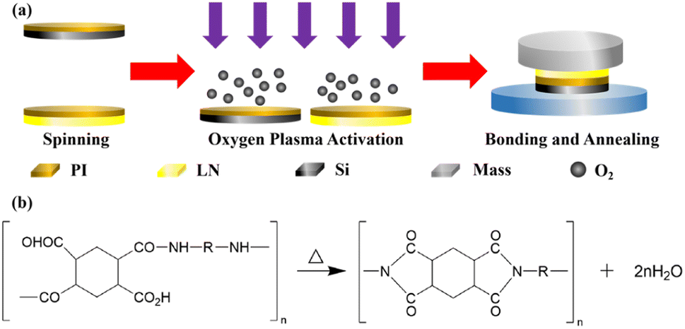
Pressure sensors have received much research attention from many researchers in order to meet the needs of people from all walks of life for accurate, efficient, and safe pressure monitoring. Besides, with the development of material preparation technology, numerous research studies on flexible pressure sensors have emerged in recent years. Zehang Luo et al. used PVDF to prepare a capacitive pressure sensor with high sensitivity (0.43 kPa−1) for the high-resolution detection (13 dpi) of pressure distribution.1 Zaihua Duan et al. prepared a high-sensitivity (0.23 kPa−1) capacitive pressure sensor through a facile process and at low cost using a polyester conductive tape2 and a high-sensitivity piezoresistive pressure sensor with a sensitivity of 5.54 kPa−1 based on polyester fibers.3 Importantly, capacitive and piezoresistive pressure sensors require additional power to work, whereas piezoelectric pressure sensors do not need additional power. Besides, compared to other types of pressure sensors, piezoelectric pressure sensors are characterized by a wide bandwidth, passivity, good dynamic characteristics, high sensitivity, and a simple structure.4–7 Therefore, there are some reports on the study of piezoelectric modules or other self-actuated modules and their integration in capacitive8 and piezoresistive9 pressure sensors. However, compared with piezoelectric pressure sensors, these are usually complex in structure or have higher requirements for the internal structural properties of the material. Consequently, many researchers choose to study piezoelectric pressure sensors. For instance, Da Bin Kim et al. prepared piezoelectric pressure sensors that maintained high linearity in a high-pressure range by using PVDF and PET fibers.10 Abhishek Sasmal et al. improved a ZnSn(OH)6-based piezoelectric pressure sensor by doping different particles in PVDF.11 Despite the excellent performance of these reported sensors, they still struggle to meet the development trends for large-scale integration in industry. Moreover, because the materials used to prepare these sensors are specialized, this field is still relatively immature as relatively less research has been performed to date in this area. Consequently, it is challenging to integrate these materials with mature technology and to fabricate sensors with multiple functions by themselves. However, LiNbO3 single crystals are an attractive piezoelectric and ferroelectric material with excellent piezoelectric, ferroelectric, thermoelectric, nonlinear optical, electro-optical, and acousto-optical properties, and are widely used in modulators, detectors, sensors, integrated optics, nonlinear optics, information storage, and other devices.12–16 LiNbO3 single crystals are widely used in optics and are called “optical silicon” owing to their unique electro-optical, acoustic-optical, thermoelectrical, and nonlinear optical properties.17 Meanwhile, LiNbO3 is widely used in the preparation of acoustic surface wave and bulk acoustic wave devices because of its high-quality factors and large electromechanical coupling coefficient.18 Besides, LiNbO3 is also a ferroelectric material with a wide range of applications due to its high piezoelectric coefficient, Curie temperature, and electro-optical coefficient.19 All the merits of LiNbO3 indicate that it could be expected to allow realizing the integrated preparation of multifunctional devices on a single lithium niobate wafer in the future. Therefore, this research studied piezoelectric pressure sensors based on the LiNbO3 material.The common preparation methods of LiNbO3 with different thicknesses are mainly thermal evaporation, liquid-phase epitaxy technology, chemical vapor deposition, sol–gel method, pulsed laser deposition, and the smart cut method. However, these epitaxial methods to prepare LiNbO3 mentioned above have many shortcomings, such as poor uniformity, physical properties, and chemical properties.20–28 In addition, the properties of the LiNbO3 prepared by the smart cut method are inferior to those of LiNbO3 single crystals, because ion aggregation and lattice damage can occur at the highest ion concentration after the ion-implantation process. These shortcomings will result in a degradation of LiNbO3's ferroelectricity.29–32 Besides, fragmentation can occur in samples, due to a discrepancy in the coefficient of thermal expansion between LiNbO3 and Si, resulting in low productivity. In addition, these preparation methods generally are applied for film preparation while LiNbO3 is a hard and brittle material, which indicates that samples prepared by the above methods are not suitable for relatively high-pressure measurements. However, chemical mechanical polishing (CMP) is an ultra-precision machining technology that could represent an important way to process LiNbO3 single crystals. CMP comprises mechanical lapping and chemical mechanical polishing. Besides, CMP processes cause minimal damage to the surface of LiNbO3 single crystals and there is no need for high-temperature annealing.33 In addition, the material is rubbed in a relative motion on a rotating polishing pad under pressure to achieve material processing. Besides, the slurry, which consists of submicron level abrasive particles and substances that can corrode the material, is dropped at the interface between the material and the polishing pad. The process of creating LiNbO3 single crystals is achieved by the combination of mechanical contact with the abrasive particles and chemical corrosion.34 In this way, not only can the problems mentioned above be effectively prevented, but also the processing needs can be met.
The integration of MEMS devices and integrated circuit devices has gradually become a new trend with the development of miniaturization and integration of devices and the development of MEMS technology and integrated circuit (IC) technology. Junfeng Sun of Southeast University adopted a similar Post-CMOS integration method to realize the monolithic integration of an RF MEMS switch and IC high-voltage driver chip.35 Therefore, it would be meaningful to prepare and test silicon-based LiNbO3 heterogeneous integrated devices. Currently, the homogeneous or heterogeneous integration of different semiconductors and silicon is usually achieved through direct bonding, which has been widely used in the manufacture of silicon-based devices.36–38 In a typical direct bonding process, high-temperature (>800 °C) annealing is usually used to achieve sufficient bonding strength, but such a high annealing temperature can lead to structural and interface damage.39 In order to reduce the annealing temperature, researchers have developed a variety of methods, such as wet bonding, vacuum ultraviolet-light activation bonding, and plasma activation bonding.40,41 Plasma activation bonding, which can make the bonding interface possess a higher surface energy, is achieved mainly by oxygen, nitrogen, and argon gas to activate the surface of the material.42 Jikai Xu et al. achieved a sample with a high bond strength after plasma activation annealing at 200 °C, with the bond strength comparable to the sample obtained by a conventional high-temperature annealing method.43 However, the coefficient of thermal expansion of LiNbO3 at room temperature is 16.7 × 10⁻⁶/°C, while the coefficient of thermal expansion of silicon is 2.5 × 10⁻⁶/°C, and a high temperature of 200 °C can still easy lead to the fragmentation of LiNbO3 during annealing due to the large differences in their coefficients of thermal expansion. So, the heterogeneous integration of LiNbO3 and silicon needs to be carried out at low temperatures. Polymer indirect bonding is a technology that allows different materials to be bonded together by polymers, offering the advantages of a relatively low-temperature, simple process, and few requirements of the material surface. So, this technology is suitable for standard CMOS bonding or different materials bonding. Xiangyu Yang et al. realized the heterogeneous integration between silicon and LiNbO3 at an 80 °C annealing temperature with a relatively high bonding intensity.44
In this study, CMP technology was used to process LiNbO3 single crystals into different thicknesses. In addition, the influences of the rotational speed of the polishing disk, the polishing fluid flow, thinning rate, and interface state were studied to better determine the CMP process parameters. The quality of the surface was assessed by XRD and AFM, which showed that there were no extra impurities introduced into the prepared surface during the CMP process and the prepared surface possessed a low roughness, which would barely influence the later processes. Likewise, low-temperature polymer heterogeneous integration technology was used to product silicon-based LiNbO3 heterogeneous integrated sheets. The quality of the heterogeneous integration interface was characterized by SEM and tensile tests, which showed that the heterogeneous integration interface was flat and tight and possessed a relatively high bonding intensity. Meanwhile, interdigital electrodes of different sizes were introduced to study the influence of the charge output and different electrode sizes, which showed that the electrodes with larger sizes had a higher charge output. The properties of piezoelectric pressure sensors based on LiNbO3 single crystals were tested by a self-built test platform. Besides, the influences of different thicknesses, electrode areas, and heterogeneous integration were illustrated by the test results, and showed that the integration of LiNbO3 and Si could dramatically improve the charge output of devices.
Materials and methods
Y-128-cut LiNbO3 wafer (CETC Deqing Huaying Electronics Co., Ltd) was used to prepare different thicknesses of LiNbO3 single crystals. The photoresist (Suzhou Research Materials Microtech Co., Ltd) was spun on a super-flat glass plate and the plate with the photoresist was prebaked at 100 °C for about 50 s for ensuring a better connection between LiNbO3 and the plate. The photoresist was mainly used to bond the materials and plate, and the photoresist could be easily removed simply by applying acetone solution after finishing the CMP process. So, if there are other adhesives that can provide enough bonding strength that do not lead to de-bonding during CMP process, and can be easily removed after CMP process, these adhesives can also be used for bonding between the plate and materials. After prebaking the plate, the LiNbO3 wafer was first put on the plate and then hand-pressed. Later, the plates were put in a bonding machine at 30 °C for 40 min to realize a sufficient bonding strength between LiNbO3 and the plate. Meanwhile, Al2O3 powder (Logitech Ltd) with a grain size of 9 μm and 1 μm was put into two specialized buckets, and water was put into both buckets to prepare Al2O3 slurry for the thinning process. Then, a specialized iron block was put on the thinning machine and the Al2O3 slurry with a 9 μm grain size was dropped on the thinning plate to repair the thinning plate at 70 rmp for about 1 h. After the repair process, the back of the glass plate with LiNbO3 was fixed on a special device by vacuum. Then, a special device was put on the thinning plate with the surface of LiNbO3 in contact with the thinning plate at 40 rmp. Besides, a simple digital display device on the special device roughly showed how much LiNbO3 had been removed. When the thickness of the LiNbO3 approached the target thickness, the Al2O3 slurry with 9 μm grain size was exchanged with 1 μm grain sized material to thin the remnant thickness. This was important because the smaller grain size could help make a flatter surface for the processed materials, which could allow a better polishing effect in the next process. After the thinning process, the processed LiNbO3 was washed by water and dried by N2. Then, SiO2 solution (Suzhou Research Materials Microtech Co., Ltd) and water were used to prepare the polishing solution. Similarly, the repair process was also needed during the polishing process and the steps for the repairing and fixing were the same as for the thinning process. Generally, to realize a smooth surface, the polishing process was processed for 10 h. After the CMP process, the glass plate was put in acetone solution for 24 h to realize the de-bonding between the LiNbO3 and the glass plate. Then, the processed LiNbO3 was put in alcoholic solution to remove the remaining acetone, and was later washed by water and dried by N2. A schematic diagram of the CMP machine is provided in Fig. 1a.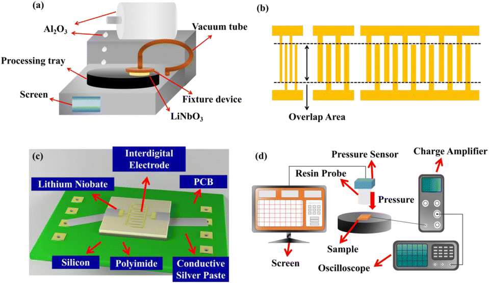 | ||
| Fig. 1 Schematic diagrams of the (a) CMP machine, (b) interdigital electrodes, (c) fabricated sensors, (d) and measurement system. | ||
Y-128 cut LiNbO3 at 500 μm thickness and silicon (Suzhou Research Materials Microtech Co., Ltd) were used to realize the low-temperature heterogeneous integration of the polyimide (PI). The PI (Wuxi Feynman Technology Co., Ltd) was taken from the freezer and put in a tube and the tube was centrifuged to remove the bubbles from the PI. Besides, the PI was allowed to stand for about 8 h to improve the activity. The LiNbO3 and silicon single crystals were washed with deionized water and dried by nitrogen. Then, the PI was spun on LiNbO3 and silicon at 3500 rmp, respectively. Also, the samples were prebaked at 80 °C for 30 s making PI into a viscoelastic phase to ensure that the heterogeneous integration interface was close enough. The surfaces to be bonded were activated through oxygen plasma activation at 300 W for 2 min. Then, LiNbO3 and silicon were prebonded together on a bonding machine at 35 °C for 2 h to ensure sufficient contact of PI. After that, the prebonded samples were put on a hot plate with a mass block on top. Besides, the temperature of the hot plate was slowly increased from room temperature to 80 °C at a rate of 0.1 °C min−1 for 24 h and then decreased slowly from 80 °C to room temperature at a rate of 0.1 °C min−1 to finish the annealing process and to reduce the residual stress, because excessive residual stress may result in a fragmentation of the pressure sensor at lower pressure or even micro-pressure. Besides, the action of slowly increasing and decreasing the temperature prevents fragmentation of heterogeneous integration samples caused by dramatic temperature variation because of the different coefficients of thermal expansion between different materials.
The electrodes were prepared on the surfaces of LiNbO3 with different thicknesses and heterogeneous integration samples by magnetron sputtering, photoetching, and ion beam etching processes, respectively. The specific steps were as follows. The prepared samples were placed in a magnetron sputtering chamber and 20/100 nm Cr/Au was deposited on the surface of the samples at 500 W. The photoresist was spun on the metal layer at 3000 rmp for 2 min, and later photoetched by a lithography machine, and then placed in developing liquid for 55 s to obtain the mask layer. The samples with a metal layer and mask layer were put in an ion beam etching chamber to remove excess metal materials. Finally, acetone was used to remove the superfluous photoresist, and then absolute ethyl alcohol to remove the acetone, before finally rinsing with deionized water to rinse out the impurities from the samples surface to finish the electrode preparation. A schematic diagram of the interdigital electrode is shown in Fig. 1b. The different structures of electrodes had the same interdigital distance of 30 μm and overlap length of 1000 μm. Besides, in this paper, the overlap area of interdigital electrodes is the product of overlap length, interdigital width and the number of interdigital. So, the 0.2 mm2 overlap area refers to that the interdigital width is 10 μm and the number of interdigital is 20. Likewise, both of 0.6 mm2 and 1.8 mm2 have interdigital widths of 30 μm, and the number of 0.6 mm2 and 1.8 mm2 are 20 and 60, respectively.
As can be seen in Fig. 1c, the heterogeneous integration samples were put on a printed circuit board (PCB) that was used for soldering the wires to connect to the charge amplifier, with the sample electrodes connected to the PCB by conductive silver paste. This set up was followed because the LiNbO3 single crystals would not have been able to withstand the high temperature of the soldering process. In addition, the sensors of the samples with different thicknesses had similar structures, as shown in Fig. 1c. In addition, the size of the samples on the PCB was about 1.2 × 1.2 cm and the size of the PCB was about 2.1 × 3.5 cm. As can be seen in Fig. 1d, the fabricated sensors were put on the platform and pressed by a compression-testing machine through a resin probe composed of Teflon. Besides, the output signal of the prepared sensors was captured and amplified by the charge amplifier and then transmitted to an oscilloscope.
Results and discussion
Fig. 2a presents a schematic diagram of the LiNbO3 single-crystal thinning process. Fig. 2b shows the thickness of the prepared LiNbO3 single crystals characterized by a step meter. The physical removal of material from the LiNbO3 surface was mainly based on the interaction between the single crystal, polishing disk, and polishing solution. The interactions can be divided into three types:45 (1) indirect contact condition, where the single crystal and polishing disk slip past each under the effect of the polishing solution and the removal is finished by the force generated by fluid motion;46,47 (2) mixed condition, where the contact type between the single crystal and polishing disk alternates between indirect contact and direct contact during the removal process;48,49 (3) direct condition, where there is little polishing solution existing at the interface between the single crystal and polishing disc, and the removal is realized by the friction caused between the single crystal and polishing disc.50,51 Fig. 2c illustrates the removal rate under different slurry flow rates. The maximum removal rate occurred when the slurry flow rate was 2 ml min−1 and the pad speed was 40 rmp, because the interface between the material surface and pad was in a mixed condition with an optimal balance between physical removal and chemical removal. The chemical removal dominated when the slurry flow rate was 2 ml min−1 and the pad speed was 30 rmp, so, in this condition, the removal rate declined due to the insufficient physical removal. Likewise, the removal rate also declined due to the insufficient chemical removal under the condition that the slurry flow rate was 2 ml min−1 and the pad speed was 50 rmp. Besides, this phenomenon could be also observed whether the slurry flow rate was 1 ml min−1 or 5 ml min−1, and the optimal removal rate was different with different combinations of slurry flow rate and pad speed. Therefore, realizing a high removal rate should be attempted in a mixed condition with an optimal balance between physical removal and chemical removal, while excessive physical removal or chemical removal is adverse to the removal rate.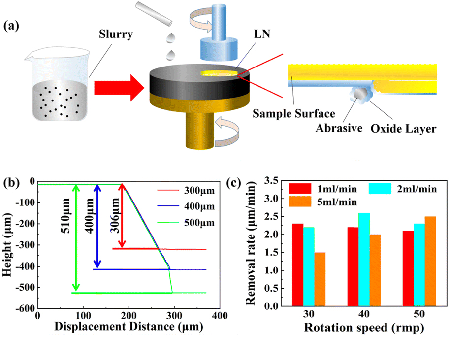 | ||
| Fig. 2 (a) Schematic diagram of the CMP process, (b) thickness illustration using a step meter, (c) and the removal rate under different conditions. | ||
Some surface material of the samples was removed by the action of abrasive particles, which means that a certain degree of lattice damage to LiNbO3 may occur during thinning process. The surface lattice properties of monocrystalline materials can be characterized by XRD analysis. The main working principle is that X-ray irradiation on the surface of the sample interacts with the sample, triggering its diffraction inside the lattice. The optical path difference of the diffracted light can be determined by using Bragg's equation:
2d![[thin space (1/6-em)]](https://www.rsc.org/images/entities/char_2009.gif) sinθ = nλ sinθ = nλ
| (1) |
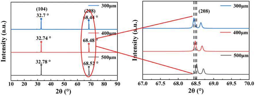 | ||
| Fig. 3 XRD characterization of LiNbO3 of 300, 400 and 500 μm thicknesses. | ||
AFM can be used to characterize the surface morphology of samples at a high resolution, and so here was used to quantitatively characterize the level of surface flattening of the ground samples. Fig. 4a–c show the surface roughness of the 500, 400, and 300 μm LiNbO3 samples measured by AFM. Fig. 4d shows the quantitative values for the contour arithmetic mean deviation (Ra) and root mean square (RMS). The results show that the thinning process did not have much effect on the surface roughness of LiNbO3, and the Ra values for the 300 and 400 μm samples were only 284 and 225 pm, respectively, while the Ra value for the 500 μm was 171 pm, demonstrating that the obtained LiNbO3 single crystals would meet the standard for practical applications in terms of their surface condition.
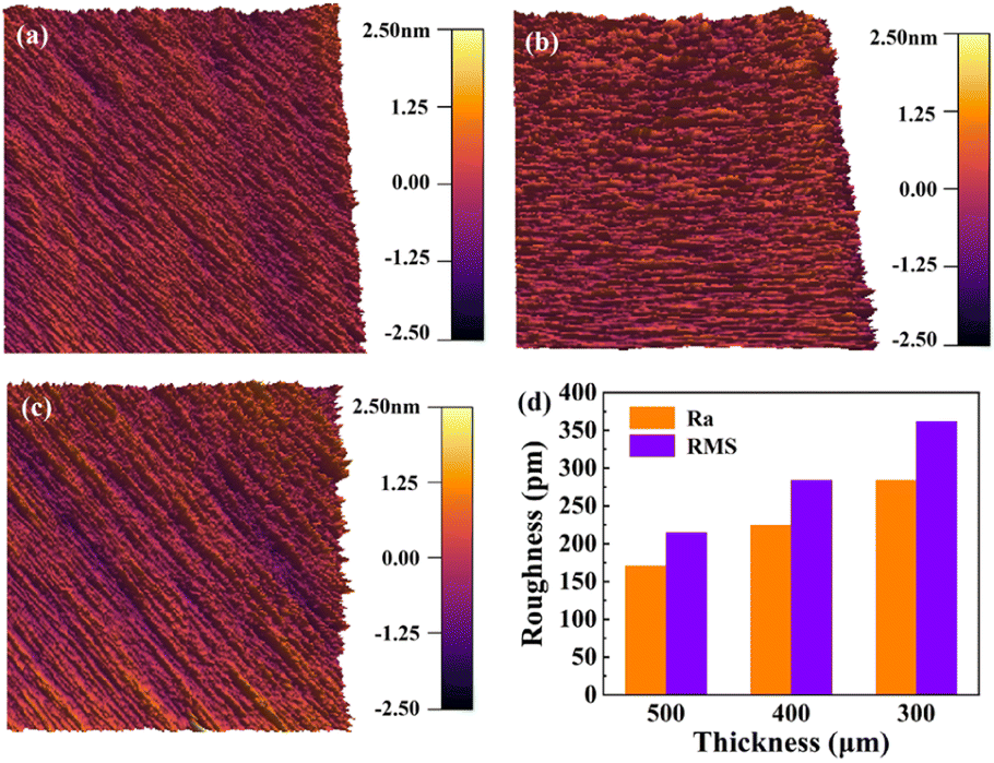 | ||
| Fig. 4 AFM characterization of LiNbO3 of 300, 400 and 500 μm thicknesses. (a–c) AFM characterization of the surfaces. (d) Ra and RMS values of the different thicknesses. | ||
Fig. 5a shows the process for the heterogeneous integration, in which the polyimide used for the heterogeneous integration was a thermoset material and in the form of polyamide acid (PAA). Fig. 5b shows the chemical equation for the polyimide solidification process,52 indicating that polyimide will generate a by-product vapor, which can lead to bubbles forming in the interface, a low bonding intensity, and a decrease in the heterogeneous integration areas. In order to decrease the amount of by-product and guarantee an excellent heterogeneous integration interface, the polyimide to be coated on the surface of samples should be prebaked during the heterogeneous integration to remove any solvent, realizing solidification to a certain extent together with a certain adhesion. However, with the extent of solidification deepening, the adhesion of the polyimide decreases. Therefore, oxygen plasma activation was introduced to activate the polyimide surface to enhance the surface energy to realize the prebonding.
 | ||
| Fig. 5 Heterogeneous integration preparation process. (a) Schematic diagram of the heterogeneous integration process. (b) Formula showing the heating process to prepare polyimide. | ||
Plasma is mainly composed of ions, electrons, photons, and free radicals. In a high-frequency alternating electric field, the electrons are accelerated and collide with plasma gas leading to the generation of free radicals, ions with positive charges, and more electrons.53 Besides, it is hard for ions to be accelerated continuously in a high-frequency alternating electric field, because ions have more mass than electrons and thus finally accumulate on the surfaces of materials, benefiting the bonding process.54 Plasma activation bonding mainly relies on the improvement of the surface hydrophilicity of a material to achieve the bonding process. Besides, the bonding process mainly relies on the hydrogen bonds formed between the water molecules absorbing to the surface and the van Waals force between the active groups generated by activation. Therefore, after plasma activation, the hydrogen bonds and van der Waals forces of the reaction are gradually transformed into covalent bonds to generate greater binding energy, thereby increasing the bonding strength and finally completing the bonding process.
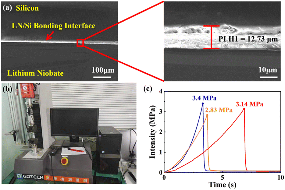
Fig. 6a shows the SEM characterization of the heterogeneous integration interface, from which it can be seen that the thickness of the polyimide adhesive at the bonding interface was approximately 12.73 μm. Besides, the heterogeneous integration interface was flat and tight between Si and LiNbO3, which proved that the two layers of polyimide films had already penetrated into each other and cross-linked together. Fig. 6b shows the tensile tester instrument used to test the bonding intensity. Fig. 6c shows the average bonding intensity was 3.12 MPa, which was not only high enough to prevent de-bonding occurring during the CMP process, but also low enough to prevent LiNbO3 or silicon shattering during the heterogeneous integration process.
 | ||
| Fig. 6 Heterogeneous integration characteristics. (a) SEM of a cross-section, (b) tensile tester, (c) results of the bonding intensity. | ||
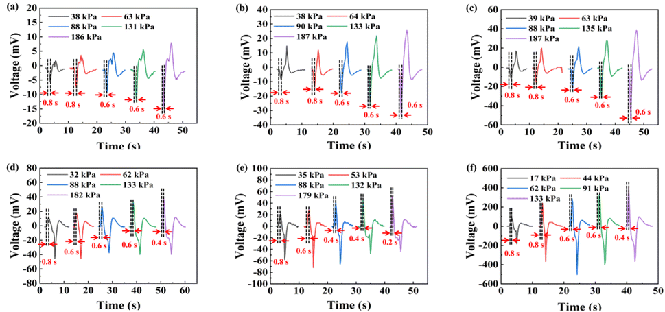
Interestingly, the phenomenon in which the output signal increased with the overlap area of the interdigital electrode increasing was observed, as shown in Fig. 7a–c, mainly because electrodes with larger areas can capture and transmit more charges. Besides, the output signals for different thicknesses were measured, as demonstrated in Fig. 7b, d and e. According to the results, samples with lower thickness were more sensitive than the larger ones, mainly because they were more likely to suffer from deformation of the materials, leading to relatively more displacement of lattice, thus leading to a relatively high electric dipole moment, which finally improved the output signal of the prepared sensors. According to Fig. 7f, an obvious enhancement of output signal was observed after heterogeneous integration. Actually, the piezoelectric effect was induced by the asymmetry of the crystal structure, and the sample was pulled by the force of the heterogeneous integration, leading to the variations in the crystal structure increasing relative to the change amount of the electric dipole moment. Therefore, more charges were generated by larger electric dipole moments, leading to the higher output signals of the heterogeneous integration samples.
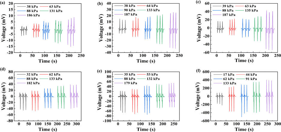 | ||
| Fig. 7 Output signal waveform diagram. (a–c) Results for different electrodes areas of 0.2, 0.6, and 1.8 mm2. (d and e) Results for different thicknesses of 400 and 300 μm; (f) results for the heterogeneous integration sample. | ||
For better comparison of the output signals the between samples with different structures, the peak of the output signal was plotted as a linear fit error bar curve, as shown in Fig. 8. The least-squares method was introduced to linear fit the data points with the characteristic equation:
| Y = a + bx | (2) |
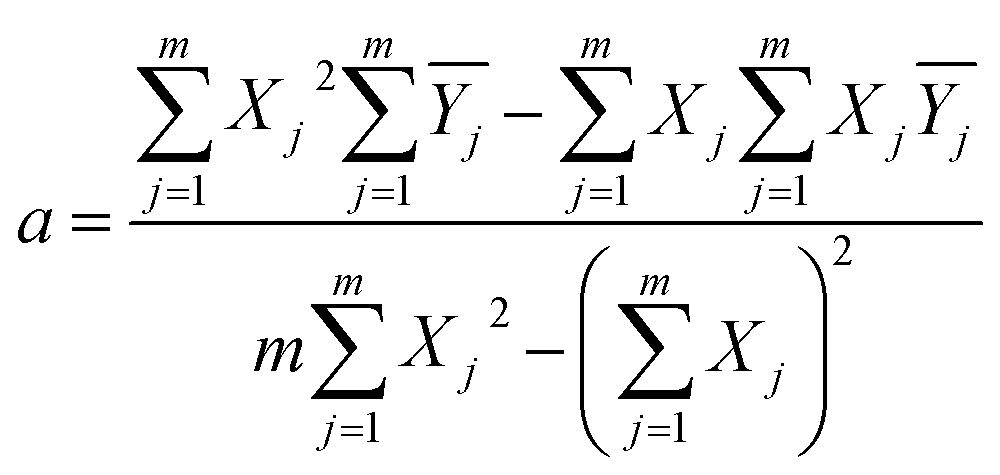 | (3) |
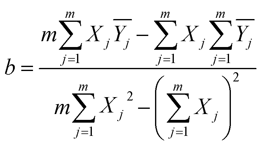 | (4) |
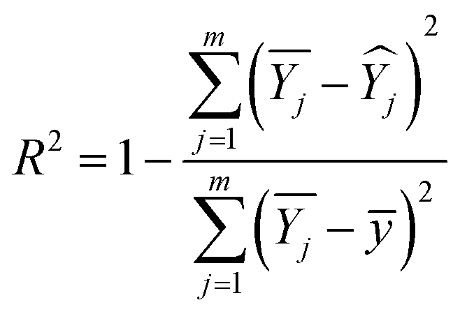
 represents the average value of the output of the JTH data point, m refers to the number of test points, and Xj is the input pressure of the JTH data point. In addition, the determination coefficient (R2) was considered to represent the linearity of fitting a straight-line and R2 was calculated by:
 | (5) |
 represents the average value of the output of the JTH data points,
  refers to the output value on the linear fitted line, and ȳ is the output value corresponding to the center point on the linear fitting line. So, the value of R2 determines the fitting effect from the characteristic equation and model, and the fitting effect is positively related to the proportion of explanatory variables in the characteristic equation that can correctly explain the value of the data points. Therefore, when the explanation rate of the explanatory variable to the predictor variable is larger, the determination coefficient is larger, and the fitting effect between the characteristic equation and the sample model is better.
 | ||
| Fig. 8 Linear fit error bar curve. (a) Comparison of different electrodes areas, (b) comparison of different thicknesses, (c) comparison between the heterogeneous integration and original sample. | ||
According to Fig. 8a, the sensitivities of the different electrodes were 0.059, 0.160, and 0.268 mV kPa−1. Besides, the sensitivity of the 1.8 mm2 electrode area was increased by 354.24% and 67.5% compared to the 0.2 mm2 and 0.6 mm2 electrode areas, respectively. In addition, the R2 value demonstrated that these sensors had excellent linearity. According to Fig. 8b, the sensitivities of the 300, 400, and 500 μm thicknesses were 0.218, 0.177, and 0.160 mV kPa−1, respectively, and the enhancements of the sensitivities were 10.63% and 36.25%, respectively, from the 500 μm to 300 μm samples. In addition, the R2 value declined in the processed samples, because the relatively low surface evenness induced an offset of the output signal compared to the unprocessed LiNbO3. According to Fig. 8c, the sensitivity of heterogeneous integration was about 16.06 times that of the original sample. The great enhancement was realized by the structural change due to the high “prestress” just as mentioned above. In addition, the data points seemed to meet a parabola caused by the relationship between the nominal stress and pressive strain exhibiting a nonlinear dependence,55 leading to the relatively low R2 value. A comparison of the results from our study with other research is shown in Table 1.
Generally, the response time is one of the most important indicators of piezoelectric pressure sensors, because the shorter the response time of the pressure sensor, the more quickly information can be obtained about pressure changes, so that the device can respond more quickly, thus reducing the occurrence of accidents. According to Fig. 9, the response time decreased as the pressure increased, mainly because the high pressure was set at a relatively fast speed, otherwise the high pressure could not be detected precisely at low speed. According to Fig. 9a–c, the electrodes area did not influence the response time, because different areas of electrodes did not influence the crystal structure when LiNbO3 was pressed. According to Fig. 9b, d, and e, the response time performance improved with the thickness of LiNbO3 decreasing, mainly because the pressure could be more easily propagated in a thinner material than in a thicker material, which means that all the lattices within the thinner material would complete the displacement faster, leading to less time required for the sample to reach the output peak. According to Fig. 9f, an enhancement of the response time was also observed in the heterogeneous integration sample. Generally, the pressure caused by PI is a kind of dynamic balancing force and has a tiny variation near equilibrium. So, the atoms in LiNbO3 were in a dynamic rather than a static state, which means that the atoms did not need time and energy to change from the static to dynamic state when another pressure was applied on the sample. Therefore, the heterogeneous integration sample displayed an improved response time performance compared to the 500 μm LiNbO3 sample.
 | ||
| Fig. 9 Response time under different pressures. (a–c) Results for samples with overlap areas of 0.2, 0.6, and 1.8 mm2, (d–f) results for samples with 400 and 500 μm thicknesses, (e) results for the heterogeneous integration sample. | ||
Conclusions
In this paper, LiNbO3 single crystals of different thicknesses were prepared by CMP technology, and their surfaces were characterized by XRD and AFM. The heterogeneous integration samples were prepared by a low-temperature polymer heterogeneous integration technique, and the heterogeneous integration interface was characterized by SEM. Both the surface and heterogeneous integration interface characterizations showed that the prepared materials had excellent performances in terms of a compact interface, and Ra values of 284 and 224 pm. The effect of different interdigital electrodes, different thicknesses of LiNbO3, and heterogeneous integration on the performance of piezoelectric pressure sensors was investigated. The results showed that the heterogeneous integration had the greatest effect on the sensitivity enhancement, which was about 15.06 times higher than that of the unbonded sample, and the thickness of LiNbO3 had a relatively low effect on the sensitivity.Author contributions
Wenhao Xu: investigation, methodology, formal analysis, writing – original draft. Wenping Geng: conceptualization, investigation, validation, writing – review & editing. Huiyi Zhang: conceptualization, validation. Wenxiao Fu: methodology, validation. Zihan Wang: investigation, validation. Jiahe Li: conceptualization, writing – review & editing. Yichi Zhang: Methodology. Xiaojun Qiao: investigation. Xiujian Chou: resource, writing – review & editing, supervision, project administration, funding acquisition.Conflicts of interest
There are no conflicts to declare.Acknowledgements
This work was supported in part by the National Natural Science Foundation of China (62171415), and Fundamental Research Program of Shanxi Province (202203021223005, 202203021222068), and Fund Program for the Scientific Activities of Selected Returned Overseas Professionals in Shanxi Province (20230015) and The Central Guidance on Local Science and Technology Development Fund of Shanxi Province (YDZJSX20231A028).References
- Z. Luo, J. Chen, Z. Zhu, L. Li, Y. Su, W. Tang, O. M. Omisore, L. Wang and H. Li, ACS Appl. Mater. Interfaces, 2021, 13, 7635–7649 CrossRef CAS PubMed.
- Z. Duan, Y. Jiang, Q. Huang, Z. Yuan, Q. Zhao, S. Wang, Y. Zhang and H. Tai, J. Mater. Chem. C, 2021, 9, 13659–13667 RSC.
- Z. Duan, Y. Jiang, Q. Huang, S. Wang, Q. Zhao, Y. Zhang, B. Liu, Z. Yuan, Y. Wang and H. Tai, Cellulose, 2021, 28, 6389–6402 CrossRef CAS.
- S. Y. Jeong, W. S. Hwang, J. Y. Cho, J. C. Jeong, J. H. Ahn, K. B. Kim, S. D. Hong, G. J. Song, D. H. Jeon and T. H. Sung, Energy, 2019, 177, 87–93 CrossRef.
- A. Rahaman, C. H. Park and B. Kim, Sens. Actuators, A, 2020, 311, 12 CrossRef.
- S. Z. Shi, W. P. Geng, K. X. Bi, J. He, X. J. Hou, J. L. Mu, F. Li and X. J. Chou, Sens. Actuators, A, 2020, 313, 9 CrossRef.
- P. Sturesson, Z. Khaji, L. Klintberg and G. Thornell, IEEE Sens. J., 2017, 17, 2411–2421 CAS.
- P. Maiti, A. Sasmal, A. Arunachalakasi and R. Mitra, ACS Appl. Electron. Mater., 2023, 5, 4968–4983 CrossRef CAS.
- Q. Huang, Y. Jiang, Z. Duan, Y. Wu, Z. Yuan, M. Zhang, Q. Zhao, Y. Zhang, B. Liu and H. Tai, Nano Energy, 2023, 118, 108997 CrossRef CAS.
- D. B. Kim, J. Han, S. M. Sung, M. S. Kim, B. K. Choi, S. J. Park, H. R. Hong, H. J. Choi, B. K. Kim and C. H. Park, npj Flexible Electron., 2022, 6, 69 CrossRef CAS.
- A. Sasmal, S. Maity, P. Maiti, A. Arockiarajan and S. Sen, Chem. Eng. J., 2023, 143794 CrossRef CAS.
- G. Shixin, C. Jianhua, Y. Na, G. Yue and W. Yu, Chin. J. Lasers, 2015, 42, 1102002 CrossRef.
- Z. Liu, S. Long, Y. Zhu, W. Wang and B. Wang, J. Alloys Compd., 2021, 867, 158986 CrossRef CAS.
- W. Zhi-Bin, L. I. Ke-Wu, Z. Rui, W. Li-Fu and W. Guo-Liang, Opt. Precis. Eng., 2015, 23, 63–69 CrossRef.
- W. Geng, J. He, X. Qiao, L. Niu, C. Zhao, G. Xue, K. Bi, L. Mei, X. Wang and X. Chou, IEEE Electron Device Lett., 2021, 42, 1841–1844 CAS.
- W. Geng, X. Qiao, J. He, L. Mei, K. Bi, X. Wang and X. Chou, J. Mater. Chem. C, 2021, 9, 15797–15803 RSC.
- Y. F. Kong, F. Bo, W. W. Wang, D. H. Zheng, H. D. Liu, G. Q. Zhang, R. Rupp and J. J. Xu, Adv. Mater., 2020, 32, 14 Search PubMed.
- J. R. Carruthers, G. E. Peterson and P. M. Bridenbaugh., J. Appl. Phys., 1971, 42, 1846–1851 CrossRef CAS.
- B. Gao, M. Ren, D. Zheng, W. Wu, W. Cai, J. Sun and J. Xu, J. Synth. Cryst., 2021, 50, 1183–1199 CAS.
- V. Postnikov, V. Ievlev, I. Zolotukhin and G. Rodin, Chem. Informationsdienst, 1973, 4(46), 006 Search PubMed.
- C. Dubs, J.-P. Ruske, J. Kräußlich and A. Tünnermann, Opt. Mater., 2009, 31, 1650–1657 CrossRef CAS.
- Y. Lu, P. Dekker and J. M. Dawes, J. Cryst. Growth, 2009, 311, 1441–1445 CrossRef CAS.
- S. Margueron, A. Bartasyte, V. Plausinaitiene, A. Abrutis, P. Boulet, V. Kubilius and Z. Saltyte, Effect of deposition conditions on the stoichiometry and structural properties of LiNbO3 thin films deposited by MOCVD, Oxide Based Mater. Devices IV, 2013, 8626, 862612 Search PubMed.
- A. Simoes, M. Zaghete, B. Stojanovic, C. Riccardi, A. Ries, A. Gonzalez and J. A. Varela, Mater. Lett., 2003, 57, 2333–2339 CrossRef CAS.
- X. Wang, Z. Ye, G. Li and B. Zhao, J. Cryst. Growth, 2007, 306, 62–67 CrossRef CAS.
- M. B. Tellekamp, J. C. Shank, M. S. Goorsky and W. A. Doolittle, J. Electron. Mater., 2016, 45, 6292–6299 CrossRef CAS.
- S. Gong, L. Shi and G. Piazza, High electromechanical coupling MEMS resonators at 530 MHz using ion sliced X-cut LiNbO3 thin film, 2012 IEEE/MTT-S International Microwave Symposium Digest, Montreal, QC, Canada, 2012, pp. 1–3 Search PubMed.
- N. Courjal, B. Guichardaz, G. Ulliac, J.-Y. Rauch, B. Sadani, H.-H. Lu and M.-P. Bernal, J. Phys. D: Appl. Phys., 2011, 44, 305101 CrossRef.
- R. Huang, C. Li, T. Lan, J. Li and Z. Wang, J. Radioanal. Nucl. Chem., 2021, 327, 905–911 CrossRef CAS.
- C. Ma, F. Lu and Y. Ma, Nucl. Instrum. Methods Phys. Res., Sect. B, 2015, 342, 76–81 CrossRef CAS.
- C. Ma, F. Lu and Y. Ma, Appl. Phys. A, 2015, 118, 1233–1238 CrossRef CAS.
- S. Zafar, V. Kaushik, P. Laberge, P. Chu, R. E. Jones, R. L. Hance, P. Zurcher, B. E. White, D. Taylor and B. Melnick, J. Appl. Phys., 1997, 82, 4469–4474 CrossRef CAS.
- C.-C. Wu, R.-H. Horng, D.-S. Wuu, T.-N. Chen, S.-S. Ho, C.-J. Ting and H.-Y. Tsai, Jpn. J. Appl. Phys., 2006, 45, 3822 CrossRef CAS.
- M. Levy, R. Osgood Jr, R. Liu, L. Cross, G. Cargill III, A. Kumar and H. Bakhru, Appl. Phys. Lett., 1998, 73, 2293–2295 CrossRef CAS.
- J. Sun, Z. Li, J. Zhu, Y. Yu and L. Jiang, AIP Adv., 2015, 5(4), 041313 CrossRef.
- S. Bao, Y. Wang, K. Lina, L. Zhang, B. Wang, W. A. Sasangka, K. E. K. Lee, S. J. Chua, J. Michel and E. Fitzgerald, J. Semicond., 2021, 42, 023106 CrossRef.
- M. Yamamoto, T. Matsumae, Y. Kurashima, H. Takagi, T. Suga, S. Takamatsu, T. Itoh and E. Higurashi, Micromachines, 2020, 11, 454 CrossRef PubMed.
- Y.-S. Kim, T. H. Nguyen and S.-H. Choa, Micromachines, 2022, 13, 537 CrossRef PubMed.
- H. Moriceau, F. Rieutord, F. Fournel, Y. Le Tiec, L. Di Cioccio, C. Morales, A. Charvet and C. Deguet, Adv. Nat. Sci., 2010, 1, 043004 Search PubMed.
- X. H. Lin, G. L. Liao, T. L. Shi and L. Nie, Chin. J. Sens. Actuators, 2006, 19, 1384–1387+1403 CAS.
- C. X. Wang, X. Y. Qi, H. Fang, Q. S. Kang, S. C. Zhou, J. K. Xu and Y. H. Tian, J. Mech. Eng., 2022, 58, 122–135 CrossRef.
- M. Eichler, B. Michel, M. Thomas, M. Gabriel and C.-P. Klages, Surf. Coat. Technol., 2008, 203, 826–829 CrossRef CAS.
- J. Xu, C. Wang, T. Wang, Y. Wang, Q. Kang, Y. Liu and Y. Tian, RSC Adv., 2018, 8, 11528–11535 RSC.
- W. P. Geng, X. Y. Yang, G. Xue, W. H. Xu, K. X. Bi, L. Y. Mei, L. Zhang, X. J. Hou and X. J. Chou, Nanomaterials, 2021, 11, 10 Search PubMed.
- C. H. Zhang, X. Geng, Z. W. Li, Z. Y. Wang and Z. D. Lu, Surf. Technol., 2020, 49, 50–56 Search PubMed.
- L. Wang, P. Zhou, Y. Yan, C. Hou and D. Guo, Tribol. Int., 2021, 156, 106831 CrossRef.
- N. Zhu, F. Zheng, Y. Zhu, S. Xu and D. Zuo, Int. J. Adv. Des. Manuf. Technol., 2016, 87, 1951–1956 CrossRef.
- J. Lu, C. Rogers, V. Manno, A. Philipossian, S. Anjur and M. Moinpour, J. Electrochem. Soc., 2004, 151, G241 CrossRef CAS.
- T. Kasai, Tribol. Int., 2008, 41, 111–118 CrossRef CAS.
- Y.-R. Jeng, P.-Y. Huang and W.-C. Pan, J. Electrochem. Soc., 2003, 150, G630 CrossRef CAS.
- Y. Zhao and L. Chang, Wear, 2002, 252, 220–226 CrossRef CAS.
- G. Bower and L. Frost, J. Polym. Sci., Part A: Gen. Pap., 1963, 1, 3135–3150 CrossRef CAS.
- R. Peter, L. James Jian-Qiang and M. V. T. Maaike, Handbook of Wafer Bonding [M], Wiley-VCH Verlag GmbH & Co. KGaA, 2012 Search PubMed.
- Y. P. Fang, W. B. Luo, X. Hao, X. Y. Bai, H. Z. Zeng, Z. Shuai and W. L. Zhang, Piezoelectr. Acoustoopt., 2020, 42 Search PubMed.
- R. Chen, T. Luo, J. Wang, R. Wang, C. Zhang, Y. Xie, L. Qin, H. Yao and W. Zhou, Nat. Commun., 2023, 14, 6641 CrossRef CAS PubMed.
- N. I. Kim, M. Yarali, M. Moradnia, M. Aqib, C. H. Liao, F. AlQatari, M. Nong, X. Li and J. H. Ryou, Adv. Funct. Mater., 2023, 33, 2212538 CrossRef CAS.
- S. Chen, J. Luo, X. Wang, Q. Li, L. Zhou, C. Liu and C. Feng, Sci. Rep., 2020, 10, 8895 CrossRef CAS PubMed.
- D. Kwon, T.-I. Lee, J. Shim, S. Ryu, M. S. Kim, S. Kim, T.-S. Kim and I. Park, ACS Appl. Mater. Interfaces, 2016, 8, 16922–16931 CrossRef CAS PubMed.
- X. Wang, Y. Gu, Z. Xiong, Z. Cui and T. Zhang, Adv. Mater., 2014, 26, 1336–1342 CrossRef CAS PubMed.
| This journal is © The Royal Society of Chemistry 2024 |