
 Open Access Article
 This Open Access Article is licensed under a Creative Commons Attribution-Non Commercial 3.0 Unported Licence
Resonant Raman scattering on graphene: SERS and gap-mode TERS†
N. N. Kurus a,
V. Kalininb,
N. A. Nebogatikovaab,
I. A. Milekhinab,
I. V. Antonovaab,
E. E. Rodyakinaab,
A. G. Milekhina,
A. V. Latyshevab and
D. R. T. Zahn*c
a,
V. Kalininb,
N. A. Nebogatikovaab,
I. A. Milekhinab,
I. V. Antonovaab,
E. E. Rodyakinaab,
A. G. Milekhina,
A. V. Latyshevab and
D. R. T. Zahn*c
aRzhanov Institute of Semiconductor Physics (SBRAS), Lavrentjev av. 13, Novosibirsk, 630090, Russia. E-mail: ifp@isp.nsc.ru
bNovosibirsk State University, Pirogov str. 1, Novosibirsk 630090, Russia
cSemiconductor Physics and Center for Materials, Architectures and Integration of Nanomembranes (MAIN), Chemnitz University of Technology, Reichenhainer Str. 70, D-09107, Chemnitz, Germany. E-mail: zahn@physik.tu-chemnitz.de
First published on 23rd January 2024
Abstract
Nanoscale deformations and corrugations occur in graphene-like two-dimensional materials during their incorporation into hybrid structures and real devices, such as sensors based on surface-enhanced Raman scattering (SERS-based sensors). The structural features mentioned above are known to affect the electronic properties of graphene, thus highly sensitive and high-resolution techniques are required to reveal and characterize arising local defects, mechanical deformations, and phase transformations. In this study, we demonstrate that gap-mode tip-enhanced Raman Scattering (gm-TERS), which offers the benefits of structural and chemical analytical methods, allows variations in the structure and mechanical state of a two-dimensional material to be probed with nanoscale spatial resolution. In this work, we demonstrate locally enhanced gm-TERS on a monolayer graphene film placed on a plasmonic substrate with specific diameter gold nanodisks. SERS measurements are employed to determine the optimal disk diameter and excitation wavelength for further realization of gm-TERS. A significant local plasmonic enhancement of the main vibrational modes in graphene by a factor of 100 and a high spatial resolution of 10 nm are achieved in the gm-TERS experiment, making gm-TERS chemical mapping possible. By analyzing the gm-TERS spectra of the graphene film in the local area of a nanodisk, the local tensile mechanical strain in graphene was detected, resulting in a split of the G mode into two components, G+ and G−. Using the frequency split in the positions of G+ and G− modes in the TERS spectra, the stress was estimated to be up to 1.5%. The results demonstrate that gap-mode TERS mapping allows rapid and precise characterization of local structural defects in two-dimensional materials on the nanoscale.
1. Introduction
Graphene, an extraordinary material with beneficial physical, chemical, structural and optical properties, is now being put under the spotlight by researchers for a second decade.1,2 Its large surface area, high mobility of charge carriers and thermal conductivity in the layer plane, together with a unique electronic band structure, makes graphene the material of choice for the creation of electronic components, such as field-effect transistors,3,4 diodes,5–7 and flexible displays.8,9 At the same time, graphene has arisen as a perfect material for the creation of chemical and biological sensors, since the adsorption of even a single molecule on its surface leads to a local change in the resistance of the material.10–12 Surface-enhanced Raman scattering (SERS)-based sensors provide advantages over many traditional sensors in terms of sensitivity, efficiency, and portability. Plasmonic substrates in the form of highly developed nanostructured metal films have been shown to be effective for the significant enhancement of Raman scattering signals (up to 107 times) from an analyte (organic/bioorganic molecules, inorganic substances, and semiconductor nanocrystals) due to the localized surface plasmon resonance (LSPR).13–15 The fabrication of plasmonic substrates composed of highly ordered arrays of metal nanoclusters using nanolithography allows the study of resonant effects for SERS enhancement of an analyte placed on different-sized metal nanoclusters.15 For plasmonic materials, gold and silver are predominantly used. The first is an inert material and undergoes no chemical reaction under normal conditions but provides a sufficient plasmonic enhancement. The second, despite being reactive, possesses a high imaginary part of the dielectric function and thus strong plasmonic enhancement. Both materials are widely used for SERS and TERS experiments in the visible spectral range. Graphene is used in the creation of such sensors for several reasons. First, since graphene is a conductor, it is possible to excite its own plasmon, thereby multiplying the optical response due to plasmon enhancement from the analyte placed on the sensor surface.16,17 As shown previously, the effect of plasmon coupling between a metal and graphene opens up the possibility of creating highly sensitive sensor systems for detecting extremely small amounts of substances, down to the level of one molecule.18,19 Second, graphene is a suitable material for chemical passivation of the sensor surface. When a substance under study interacts with a metal structure, it leads to a shift in the vibrational modes of the analyte or the emergence of new modes in the SERS spectrum, thus making it difficult to unambiguously interpret the results.20–23 It has been shown that placing a graphene layer on the surface of a plasmonic substrate makes it possible to prevent these interactions. Finally, owing to the two-dimensional structure of graphene, the problem of smoothing the developed surface relief of the active element of the SERS-based sensor is successfully solved, resulting in the uniform deposition of the analyte and increasing the measurement accuracy.24 Thus, it is obvious that graphene is one of the key materials in plasmonics, and the physical phenomena that occur in hybrid graphene–metal structures define sensor parameters, such as the enhancement factor, sensitivity, and selectivity. For example, it was shown that mechanical strain25 and p-type or n-type doping26,27 of a graphene film appear during contact with gold or silver nanostructures. At the same time, micro- and nanocorrugations, which appear during the placing of the graphene film on a plasmonic substrate with sophisticated relief, and their effect on the mechanical and optical properties of graphene have been poorly studied. It was found that the bending of a graphene film leads to a change in its electrophysical and optical properties.28 Hence, the formation of nanofolds and corrugations in the vicinity of metal nanostructures affects LSPR conditions and consequently the enhancement of the SERS signal from the analyte.29,30 In this context, to study the effect of nanofolds and nanoscale corrugations of graphene, a technique suitable to probe the vibrational properties of the material far beyond the diffraction limit is highly required. However, to date, only a few papers devoted to the optical characterization of structural defects in graphene on the nanoscale are known.Tip-enhanced Raman scattering (TERS) is a technique31–34 important in the study of the vibrational properties of nanostructures and has two advantages over other optical techniques: a high spatial resolution down to the subnanometer level and an extraordinary enhancement of spectrum intensity by up to 1013. Being a modified version of SERS, the TERS technique exploits the surface plasmon field localized at the apex of a metalized AFM probe to enhance the Raman scattering of the vibrational modes of the material studied. The suitability of TERS for studying structural defects, impurities, and mechanical stress in graphene was previously demonstrated.35–38 The TERS of steps, ridges, and crack structures of epitaxial graphene that provide noticeable mechanical strain was investigated.35 Reversible artificial defects were induced in graphene and detected using the TERS technique.29 TERS analysis of the D mode intensity allowed the edges of both graphene36,38 and graphite regions36 or highly localised defects in graphene to be visualized with a nanometer scale resolution.37 Nevertheless, in the works cited, significant signal enhancement, being crucial in the study of nanoscale-sized structural features, was not achieved. Thus, the enhancement factor, defined as the ratio of the near-field signal intensity to the far-field signal intensity, EF = Itip down/Itip up, for the G mode was shown to be equal to 1,3 (ref. 34) and 4,2.35
To overcome the problem of a low near-field signal intensity and achieve a larger enhancement factor, ordinary TERS conditions can be modified and gm-TERS is implemented instead. In gm-TERS, the material to be studied is placed in the close gap between the metalized probe tip and metal element of a plasmonic substrate, forming a sort of metal dimer, thus making a significant enhancement of the local electromagnetic field, E, in the nanometer sized gap, called as a “hot spot”, possible. Considering that plasmonic enhancement of the Raman signal is proportional to E4, one may achieve an enhancement factor that is few orders of magnitude greater than in ordinary TERS.39,40
Previously we have shown39 that a giant enhancement (Itip down/Itip up = 7.5 × 10⁵) of phonon modes can be achieved using gm-TERS on graphene-like materials, specifically a monolayer of MoS2, and gm-TERS can be effectively applied for determining the local changes in crystal structure and doping concentration in the monolayer. Interestingly, a promising approach to use functionalized tip-enhanced Raman spectroscopy for probing the gap-mode TERS enhancement on MoS2 was demonstrated in ref. 40. At the same time, to the best of our knowledge, data on the gm-TERS of graphene are limited to only two works. Pashaee et al.38 achieved a spatial resolution below 20 nm, an enhancement factor (EF) of about 18, and visualized the edges of graphene-like crystals using gm-TERS. In our previous work,41 a spatial resolution of 10 nm and an EF of 50 allowed the visualization of nanofolds in a multilayer graphene film placed on a plasmonic substrate during gm-TERS mapping. It was shown that G and 2D mode positions of graphene in the nanofold area undergo low-frequency shifts with respect to those in flat multilayered graphene. Such a frequency shift indicates the presence of mechanical stress in nanofolds, which was estimated to be 0.7%. The results prove the suitability and possibility of using gm-TERS mapping for the study of structural features in materials at the nanoscale.
At the same time, multi-layered graphene film of a nominal thickness of 10 monolayers (MLs) was studied. Moreover, the real thickness was stated to be in the range of 2–10 MLs and may fluctuate over the sample, thus contributing to SERS or TERS measurement errors. A single layer of graphene is more favorable for the observation of an effective plasmonic enhancement of the Raman signal due to “first layer enhancement effect”,42 which should provide higher SERS and TERS enhancement. However, to realise gm-TERS from graphene, optimal experimental conditions for effective plasmonic enhancement, including structural and optical parameters of the TERS tip, plasmonic nanodisks, and substrate material, as well as the relevant excitation wavelength, should be determined.
Nevertheless, data on gm-TERS chemical mapping which could demonstrate the presence of structural defects in graphene and allow the study their properties on the nanoscale are not known.
In this paper, we report the results of plasmon-enhanced Raman scattering by a monolayer graphene film transferred from the aqueous phase onto a plasmonic substrate at micro- and nanoscales. On the basis of a SERS study, experimental conditions were established to achieve significant gap-mode TERS from a graphene film residing at plasmonic tip–Au nanodisk nanogaps. This made it possible for us to perform gap-mode TERS mapping which demonstrates the presence of mechanically stressed nanofolds of graphene located in the vicinity of plasmonic nanodisks. The approaches reported in the paper can be extended to other two-dimensional materials.
2. Materials and methods
Plasmonic substrates were fabricated using nanolithography on a Si substrate and consisted of periodic Au nanodisk arrays (period is 350 nm) with a size of 10 × 10 μm2, as described in ref. 41. A commercial monolayer graphene film on a copper substrate was transferred to the periodic arrays of Au nanodisks using a transfer method from the aqueous phase, as described in ref. 39.The thickness of the graphene film was determined from atomic force microscopy (AFM) experiments. The thickness of the graphene was obtained as about 1 nm, which is three times more than a monolayer graphene film. The discrepancy in thicknesses stated and measured is due to the transfer of the graphene film onto the rough Si/SiO2 (100 nm) substrate, being a base of the plasmonic substrate. AFM, micro-Raman (SERS), and gap-mode TERS measurements have been realized with the use of a combined AFM-Raman system (Xplora Nano) consisting of two main parts including a Horiba Omega Scope atomic force microscope and an Xplora PLUS Raman spectrometer. Alternating current (AC) mode and commercially available VIT_P probes purchased from TipsNano were used for AFM measurements.
Raman spectra were recorded in a quasi-backscattering configuration at normal light incidence with the use of an objective (100×, 0.7 NA). The diameter of the laser spot was about 1 μm, which is three times larger than the period of the nanocluster array. The Raman spectrum of the graphene film on the Si/SiO2 substrate without plasmonic structure corresponds to that of monolayer graphene, confirming the AFM results. SERS measurements were performed at excitation wavelengths of 532, 638, and 785 nm. The typical laser power in each measurement was about 1 mW to avoid any noticeable heating effects. The acquisition time in SERS measurements was 5 s.
TERS images were obtained using VIT_P probes (TipsNano), coated with silver by vacuum evaporation, as described in ref. 43. The AFM probe, with the tip displaced by 70° with respect to the sample plane, was side-exposed to the laser beam at an angle of 70°. The excitation and registration of the optical signal were performed in the quasi-backscattering geometry through an objective (100×, 0.7 NA), as described in ref. 39. A solid-state laser with a wavelength of 638 nm was exploited for TERS measurements. The laser power at the sample surface was about 1 mW. The spectral resolution in TERS experiments was about 4 cm−1. The accumulation time of the TERS signal in each pixel was 0.3 s. The signal intensity in all Raman measurements is defined as the peak height.
3. Results
3.1 SERS study of graphene on a plasmonic substrate
A typical AFM image of the graphene film on a plasmonic substrate in the form of Au nanodisks with diameters of 103 nm and a period of 350 nm is shown in Fig. 1a. As shown in the figure, the film covers the substrate and forms a lot of periodic nanoscale folds and suspended graphene areas around each nanodisk (marked in the height profile in Fig. 1b). As shown in Fig. 1, the length and width (height) of nanofolds are about 100 and 30 (3) nm, respectively. The highly ordered nanofolds predominantly occur between nanodisks nearest to each other and form a net of vertical and horizontal lines between nanodisks. As discussed in our previous work,41 nanofold formation is associated with the differences in adhesion of graphene to Au nanodisks and to the silicon substrate. Raman measurements were performed for each array with nanodisks of various sizes (from 50 to 250 nm) on the visually homogeneous areas of the sample with highly ordered folds. The nanocluster array was at least three times larger than the size of the laser spot.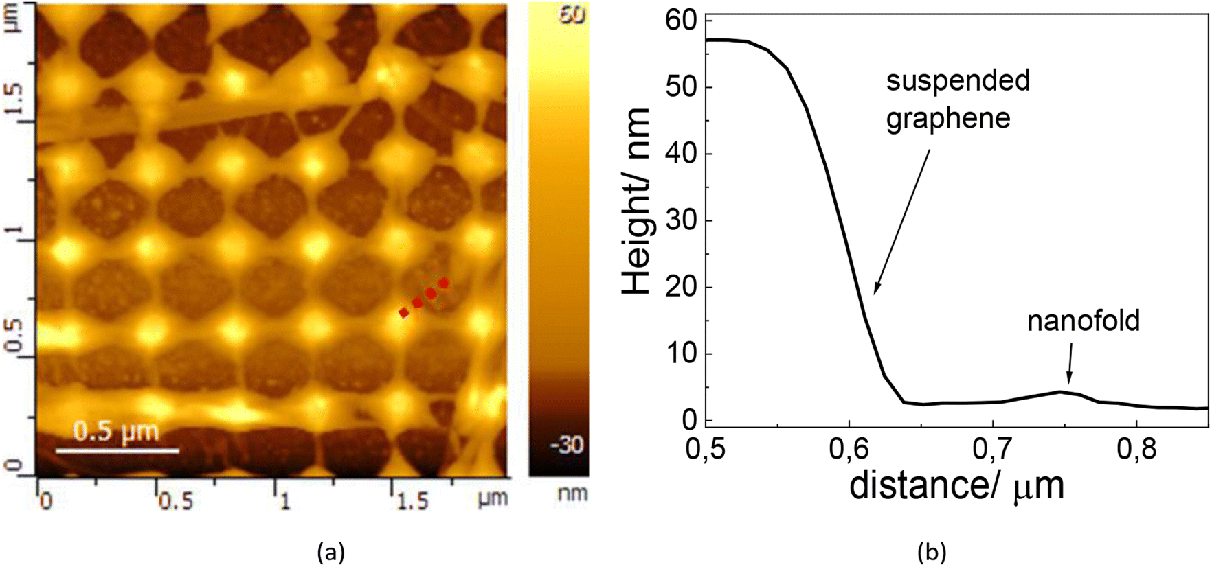 | ||
| Fig. 1 (a) AFM image and (b) height profile measured along the red dashed line in (a) of a graphene film placed on a plasmonic substrate with 103 nm gold nanodisks. | ||
The Raman spectrum of the graphene film on a bare Si/SiO2 substrate is presented in Fig. 2 (black curve) and has two main vibrational modes: the G mode at 1584 cm−1, corresponding to E2g symmetry vibrations in the plane of sp2 hybridized carbon atoms and the 2D mode at 2640 cm−1 associated with a process of two-phonon scattering involving A1g symmetry vibrations.
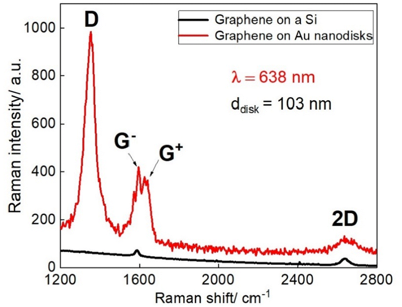 | ||
| Fig. 2 Typical SERS spectrum of graphene film on a plasmonic substrate (the diameter of gold nanodisks is about 103 nm) (red) and the Raman spectrum of the graphene film measured on a bare Si/SiO2 substrate (black) at an excitation wavelength of 638 nm. | ||
The absence of a D mode, present in the graphene Raman spectra near 1350 cm−1 due to defect-associated activation of A1g vibrations, indicates high crystallinity of the graphene film. The peak positions are in good agreement with previously published data for a single monolayer of graphene.44–46 The Raman spectrum of the graphene film on Au nanodisks (red curve in Fig. 2a) excited at 638 nm reveals the SERS enhancement of graphene Raman modes. While the 2D mode is only two times enhanced (EF ≈ 2), the enhancement factor for the G mode reaches a value of about 50 (EF ≈ 50). Importantly, in the SERS spectra, a split of the G mode into two peaks (G− at 1583 cm−1 and G+ at 1625 cm−1) is observed, indicating the presence of mechanical strain in the graphene film placed on the gold disks array. Moreover, an intense D mode emerges in the SERS spectra due to the activation of A1g symmetry vibrations caused by the formation of a large number of nanofolds in the graphene film. Note that distinguishing the contribution of the SERS effect and defect formation to the Raman enhancement of the D mode is almost not possible.
It was previously shown for a multilayered graphene film,41 that the dependence of enhancement factors on gold nanodisk diameters has a resonant character for the main vibrational modes. As expected, the same phenomenon is observed for SERS in a single-layer graphene film: resonance conditions shift to the larger diameter of nanodisks with an increase in the excitation wavelength. Fig. 3a–c demonstrate the dependence of the G mode enhancement factor on the nanodisk diameter at excitation wavelengths of 532, 638 and 785 nm, respectively. As seen in Fig. 3d, the G mode enhancement factor of graphene on a structure with gold nanodisks of about 108 nm in diameter reaches its maximum (EF = 50) upon excitation at a wavelength of 638 nm. A somewhat smaller enhancement is observed at a wavelength of 532 nm on a nanodisk diameter of about 75 nm. Upon non-resonant excitation (at 785 nm), a maximum enhancement factor of about 25 is observed for a nanodisk diameter of 120 nm.
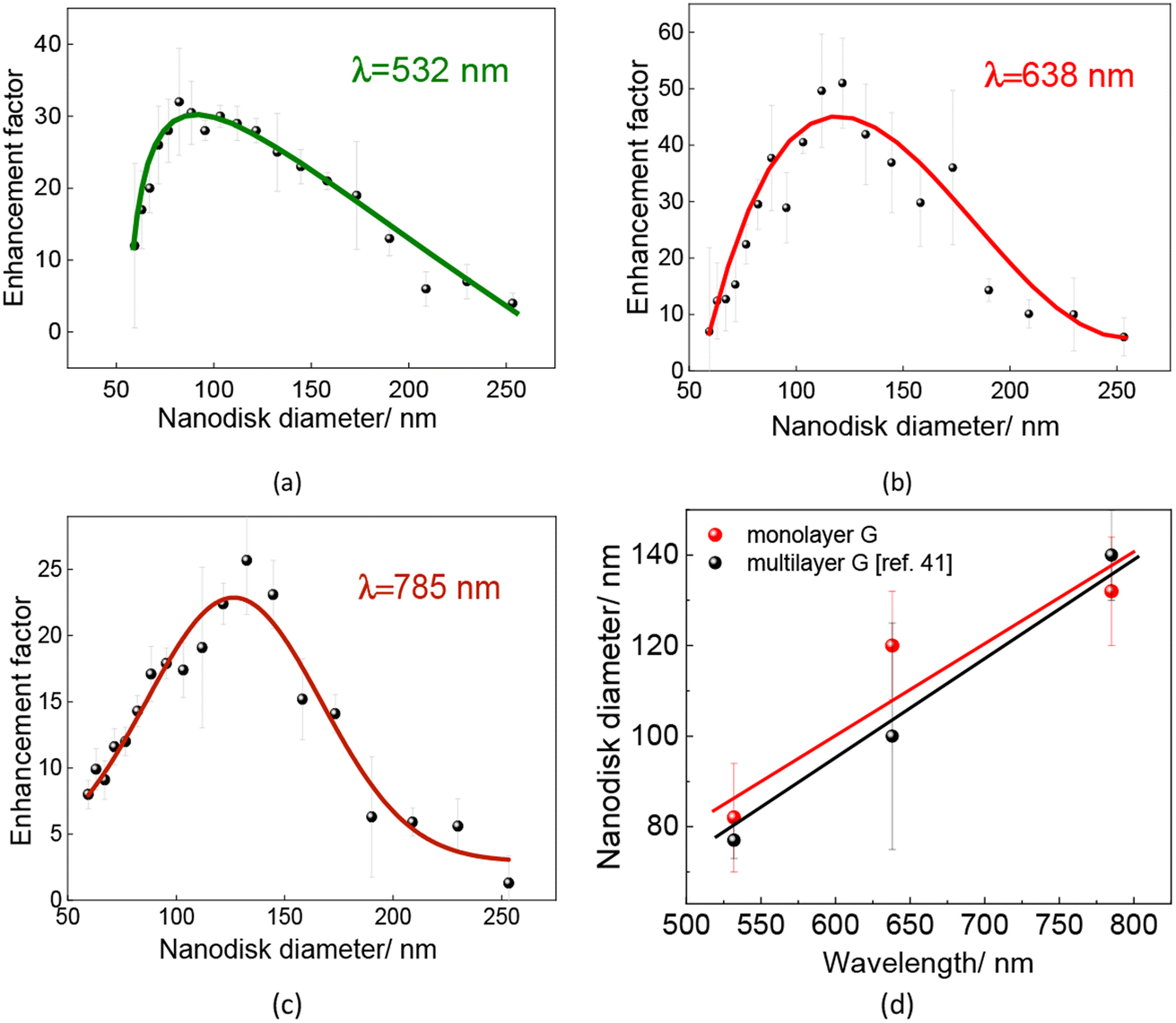 | ||
| Fig. 3 Enhancement factor (EF) of the graphene G mode measured at 532 nm (a), 638 nm (b) and 785 nm (c) as a function of the gold nanodisk diameter. (d) The diameter of gold nanodisks, corresponding to the maximum Raman signal enhancement, as a function of the excitation wavelength in comparison with the same data reported for multilayer graphene.41 The lines are a guide for the eye. | ||
Generally, these results are in good agreement with the data obtained for multilayered graphene,41 as shown in Fig. 3d, where the resonant character of the enhancement was shown, and a maximum EF was also reached at an excitation wavelength of 638 nm. We have shown earlier that a larger LSPR wavelength is observed for nanodisks with larger diameters.47 According to ref. 47, resonantly enhanced surface Raman scattering is expected for nanodisks with a LSPR wavelength in the spectral range of 500–600 nm. Most probably, the higher absorptance of larger diameter disks excited at 638 nm is responsible for the large EF relative to those excited at 532 nm.47
Note that for nanodisks under this study reveal LSPR below 700 nm and, therefore, they cannot be excited resonantly with the excitation wavelength of 785 nm, which causes weaker enhancement in off-resonant conditions.
However, in the present study, at least two times larger values of EF have been reached for all excitation wavelengths. This is apparently due to the higher crystalline perfection of the graphene film compared to multilayered graphene, as well as for its better contact with the plasmonic substrate. Another reason of higher SERS enhancement factor in graphene in comparison with multigraphene film (25 versus 4,41 respectively, for 785 nm) can be due to different effective dielectric functions of a medium surrounding Au nanodisks, which can cause a change in SERS resonant conditions and a higher EF for graphene.
3.2 Gap-mode TERS by graphene on a plasmonic substrate
An excitation wavelength of 638 nm and an array with nanodisks with diameters of about 108 nm, for which the highest plasmon enhancement of the Raman signal from graphene was observed in the SERS experiment, were chosen for performing gap-mode TERS measurements. Fig. 4 shows an AFM height image of the 2 × 2 nanodisk sample area (Fig. 4a) and the gm-TERS map of graphene corresponding to the same area (Fig. 4b). As seen in Fig. 4b, there is a consistency between the localization of the intensive G-mode signal in graphene with the height map. Thus, a significant increase in the intensity is observed at the edges of gold nanodisks. The high intensity regions on the TERS map have a semi-ring shape, which agrees well with that previously observed in gap-mode TERS of multi-layered graphene transferred to a similar plasmonic substrate.41 These regions originate from the intense electric field localized at nanodisk edges. The ring-shaped TERS images were also recorded for MoS2 monolayers placed on similar plasmonic structures.40 The asymmetry of TERS images observed can be explained if one considers the side illumination geometry39 used in our experiments. Moreover, the TERS tip is placed obliquely with respect to the sample surface. Notably, TERS images are highly reproducible for a particular TERS tip and Au disk. However, the shape of TERS images can vary from semi-rings to almost symmetrical rings.40 This depends on the flatness of Au disks and the position of the hot spot with respect to the sample surface. The gm-TERS measurements performed for another Au disk, as indicated in Fig. S2,† which shows a semi-ring TERS image with a slight difference from Fig. 4c, confirm this conclusion.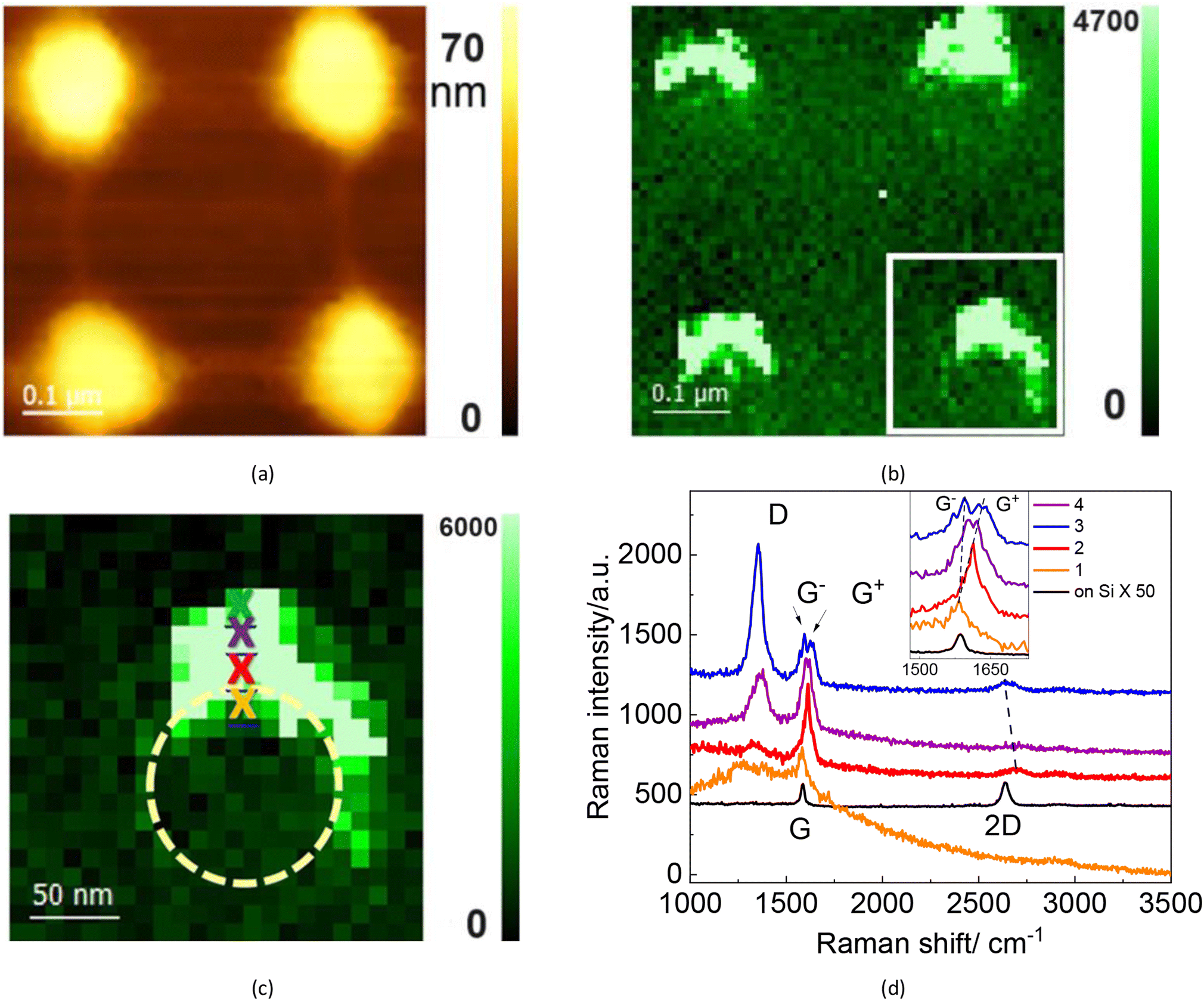 | ||
| Fig. 4 (a) AFM height map of a fragment of the Au nanodisk array (4 nanodisks) and (b) corresponding gm-TERS map of the G mode intensity. (c) Detailed gm-TERS map of the G mode intensity for a sample area of 250 × 250 nm2 (marked with a white square in (b)). A yellow dashed circle depicts the position of the gold nanodisk. (d) Gm-TERS spectra of graphene near a gold nanodisk measured at areas marked with crosses in (c). The TERS spectra and areas indicated by crosses are shown by same colors. | ||
Fig. 4c shows a more detailed TERS map of the G mode intensity in the area of one nanodisk. Very similar gm-TERS images were also obtained for the D-mode (Fig. S1 in the ESI†). As seen from Fig. 4c, the TERS map of high intensity has the same vertically elongated shape as the nanofold in the graphene film near the edge of the nanodisk seen in the AFM image (Fig. 4a). In this regard, the TERS spectra were acquired in a direction from the edge of the nanodisk and along the nanofold with a step of 10 nm, corresponding to the spatial resolution in the experiment. Fig. 4d shows the evolution of the TERS spectra with colors corresponding to the areas indicated in Fig. 4c.
As seen, in the TERS spectrum of graphene on a gold disk (orange curve), a broad plasmon peak dominates with eroding graphene peaks. The position and linewidth of the gap-mode plasmon can be seen in the TERS spectra of bare nanodisks (Fig. S3†). At the very edge of the nanodisk, an intense G mode appears (red curve) that is enhanced 20 times (EF = 20) in comparison with spectra of graphene lying on a silicon substrate (black curve). Such a significant enhancement is because the electromagnetic field distribution has a strong maximum at the nanodisk edge. When moving away from the nanodisk, the intensity of the D mode starts to increase (purple curve). The reason for this behavior is the formation of the nanofold, leading to the activation of A1g symmetry vibrations. At the same time, the G mode decreases in intensity and splits into low frequency G− (at 1600 cm−1) and high frequency G+ (at 1618 cm−1) modes, indicating the appearance of mechanical stress in the graphene film. Considering that the split is 18 cm−1, one may estimate the value of the mechanical stress to be 0.8%.48
An increase in the bending of the graphene layer further along the nanofold causes the G mode frequency split to increase to 32 cm−1, leading to an estimation of the mechanical stress to be more than 1.5% (blue curve in Fig. 4d). A higher mechanical stress in the nanofold area relative to multilayered graphene (0.7%)41 can be explained by the absence of intralayer bonds and, consequently, a lower strength material. The appearance of the D′ mode in the same spectral range as the G+ mode, could be an alternative explanation of features seen in TERS and SERS experiments. However, the appearance of the D′ mode occurs with the emergence of a 2D′ mode of comparable intensity at 3250 cm−1.49 In our TERS experiments, the 2D′ mode was not observed; therefore, we believe that this doubled feature near 1605–1620 cm−1 can be assigned to G− and G+ modes. Moreover, the splitting value between the frequency position of these modes changes gradually along the fold, confirming the strain variation. In addition, the 2D mode undergoes a low frequency shift from 2696 to 2642 cm−1 when observed in the area of folds (Fig. 4d), manifesting the presence of significant tensile strain. Conversely, the absolute frequency position of G− and G+ modes is notably higher than expected for only a strain effect. The high frequency shift of these modes could be due to charge carrier doping as discussed in ref. 50. Notably, doping causes a noticeable shift of G and D modes.51 It was already established that Au deposition induces p-doping in graphene.52 This p-type doping causes a strong and moderate high-frequency shift of G and D modes, respectively. Most probably, the superposition of the strain and doping effects are responsible for the behaviour of the modes in the TERS experiments of graphene on nanodisks. Obviously, a careful analysis that distinguishes the effects of strain and charge doping in the TERS data is required. At the same time, an intense D mode near 1350 cm−1 in the area of the graphene nanofold is observed. This mode is enhanced by a factor of 100 in comparison with that observed for flat graphene on Si. This is not only due to the SERS effect but also because of defect formation. Note that the enhancement factor for the 2D mode is only about 23, whereas EFs for G and D modes are about 20 and 100, respectively. The same enhancement of the 2D mode was observed in our previous publication (ref. 41). The maximum EF of 50 was reached for D and G modes, whereas the EF for the 2D mode was only about 10. As discussed above, a D band enhancement is due to the SERS effect and defect formation. The modest enhancement of the 2D mode may be associated with its high frequency, which is far from the LSPR energy and thus from resonance conditions.
4. Conclusions
Plasmon-enhanced Raman scattering in a graphene film transferred onto a plasmonic substrate with gold nanodisks was studied at micro- and nano-scales. The resonant character of the SERS enhancement was demonstrated. It was shown that the resonance conditions for graphene differ slightly from those in multi-layered graphene, and an effective signal enhancement could be obtained, even with excitation at 532 nm. Moreover, higher crystallinity and better mechanical contact of the graphene film with gold nanodisks allowed us to significantly increase the optical response of the material, up to an EF of 50 in comparison with an EF of 25 in the multilayered graphene.In gm-TERS experiments, a high spatial resolution (10 nm) and unprecedentedly large enhancement factor (EF = 100) made it possible to follow the changes in the Raman spectrum of the graphene film along a nanofold. It was shown that the graphene film has twice the mechanical strain of multilayered graphene due to the absence of interlayer bonds. Thus, the data presented here sheds light on the possibility of implementing gap-mode TERS to study the structural features of materials at the nanoscale.
Author contributions
Conceptualization, A. G. M., A. V. L. and D. R. T. Z.; methodology, N. A. N., I. V. A. and E. E. R.; validation, I. A. M. and D. R. T. Z.; formal analysis, N. N. K., N. A. N., I. A. M. and E. E. R.; investigation, N. N. K. and I. A. M.; resources, A. G. M., A. V. L. and D. R. T. Z.; data curation, N. N. K., V. A. K. and E. E. R.; writing – original draft, N. N. K., I. A. M., A. G. M. and D. R. T. Z.; writing – review & editing; A. G. M. and D. R. T. Z.; visualization, I. A. M.; supervision, A. G. M. and D. R. T. Z.; project administration, A. G. M. and A. V. L.; funding acquisition, A. G. M. All authors have read and agreed to the published version of the manuscript.Conflicts of interest
There are no conflicts to declare.Acknowledgements
The reported study was funded by RFBR according to the research project no. 20-52-04009.Notes and references
- K. S. Novoselov, V. I. Fal'ko, L. Colombo, P. R. Gellert, M. G. Schwab and K. Kim, Nature, 2012, 490, 192–200 CrossRef CAS PubMed.
- A. K. Geim, Science, 2009, 324, 1530–1534 CrossRef CAS PubMed.
- K. S. Novoselov, A. K. Geim, S. V. Morozov, D. Jiang, Y. Zhang, S. V. Dubonos, I. V. Grigorieva and A. A. Firsov, Science, 2004, 306, 666–669 CrossRef CAS PubMed.
- F. Schwierz, Nat. Nanotechnol., 2010, 5, 487–496 CrossRef CAS PubMed.
- M. Zeng, L. Shen, M. Zhou, C. Zhang and Y. Feng, Phys. Rev. B: Condens. Matter Mater. Phys., 2011, 83, 115427 CrossRef.
- D. Dragoman, M. Dragoman and R. Plana, J. Appl. Phys., 2010, 108, 084316 CrossRef.
- A. Sotoudeh and M. Amirmazlaghani, Superlattices Microstruct., 2018, 120, 828–836 CrossRef CAS.
- J. Lee, T. H. Han, M. H. Park, D. Y. Jung, J. Seo, H. K. Seo and S. Yoo, Nat. Commun., 2016, 7, 11791 CrossRef CAS PubMed.
- Y. Ma and L. Zhi, Small Methods, 2019, 3, 1800199 CrossRef.
- J. D. Fowler, M. J. Allen, V. C. Tung, Y. Yang, R. B. Kaner and B. H. Weiller, ACS Nano, 2009, 3, 301–306 CrossRef CAS PubMed.
- N. Mohanty and V. Berry, Nano Lett., 2008, 8, 4469–4476 CrossRef CAS PubMed.
- J. Basu, J. K. Basu and T. K. Bhattacharyya, Int. J. Smart Nano Mater., 2010, 1, 201–223 CrossRef CAS.
- I. R. Nabiev, R. G. Efremov and G. D. Chumanov, Sov. Phys. Usp., 1988, 31, 241–262 CrossRef.
- K. Kneipp, Y. Wang, H. Kneipp, L. T. Perelman, I. Itzkan, R. R. Dasari and M. S. Feld, Phys. Rev. Lett., 1997, 78, 1667–1670 CrossRef CAS.
- A. G. Milekhin, N. A. Yeryukov, L. L. Sveshnikova, T. A. Duda, E. E. Rodyakina, V. A. Gridchin, E. S. Sheremet and D. R. T. Zahn, Beilstein J. Nanotechnol., 2015, 6, 749–754 CrossRef CAS PubMed.
- X. Luo, T. Qiu, W. Lu and Z. Ni, Mater. Sci. Eng., R, 2013, 74, 351–376 CrossRef.
- J. C. Reed, H. Zhu, A. Y. Zhu, C. Li and E. Cubukcu, Nano Lett., 2012, 12, 4090–4094 CrossRef CAS PubMed.
- S. G. Zhang, X. W. Zhang, X. Liu, Z. G. Yin, H. L. Wang, H. L. Gao and Y. J. Zhao, Appl. Phys. Lett., 2014, 104, 121109 CrossRef.
- G. Sarau, B. Lahiri, P. Banzer, P. Gupta, A. Bhattacharya, F. Vollmer and S. Christiansen, Adv. Opt. Mater., 2013, 1, 151–157 CrossRef.
- Y. F. Li, F. X. Dong, Y. Chen, X. L. Zhang, L. Wang, Y. G. Bi, Z. N. Tian, Y. Liu, J. Feng and H. B. Sun, Sci. Rep., 2016, 6, 1–8 CrossRef PubMed.
- D. K. Kim, S. M. Yoo, T. J. Park, H. Yoshikawa, E. Tamiya, J. Y. Park and S. Y. Lee, Anal. Chem., 2011, 83, 6215–6222 CrossRef CAS PubMed.
- C. L. Chuang, J. N. Aoh and R. F. Din, Microelectron. Reliab., 2006, 46, 449–458 CrossRef CAS.
- K. Long, X. Luo, H. Nan, D. Du, W. Zhao, Z. Ni and T. J. Qiu, Appl. Phys., 2006, 114, 183520 Search PubMed.
- W. Xu, X. Ling, J. Xiao, M. S. Dresselhaus, J. Kong, H. Xu, Z. Liu and J. Zhang, Proc. Natl. Acad. Sci. U. S. A., 2012, 109, 9281–9286 CrossRef CAS PubMed.
- Y. Zhao, X. Liu, D. Y. Lei and Y. Chai, Nanoscale, 2014, 6, 1311–1317 RSC.
- C. H. Huang, H. Y. Lin, C. W. Huang, Y. M. Liu, F. Y. Shih, W. H. Wang and H. C. Chui, Nanoscale Res. Lett., 2014, 9, 1–5 CrossRef PubMed.
- J. Lee, K. S. Novoselov and H. S. Shin, ACS Nano, 2011, 5, 608–612 CrossRef CAS PubMed.
- A. Krayev, Nanoimaging and Nanospectroscopy VI, SPIE, 2018, vol. 10726, p. 1072609 Search PubMed.
- P. Wang, D. Zhang, L. Li, Z. Li, L. Zhang and Y. Fang, Plasmonics, 2012, 7, 555–561 CrossRef CAS.
- P. Wang, D. Zhang, L. Zhang and Y. Fang, Chem. Phys. Lett., 2013, 556, 146–150 CrossRef CAS.
- R. M. Stockle, Y. D. Suh, V. Deckert and R. Zenobi, Chem. Phys. Lett., 2000, 318, 131–136 CrossRef CAS.
- B. Pettinger, B. Ren, G. Picardi, R. Schuster and G. Ertl, Phys. Rev. Lett., 2004, 92, 096101 CrossRef PubMed.
- Z. Zhang, S. Sheng, R. Wang and M. Sun, Anal. Chem., 2016, 88, 9328–9346 CrossRef CAS PubMed.
- Y. Cao and M. Sun, Rev. Phys., 2022, 8, 100067 CrossRef.
- S. Vantasin, I. Tanabe, Y. Tanaka, T. Itoh, T. Suzuki, Y. Kutsuma, K. Ashida, T. Kaneko and Y. Ozaki, J. Phys. Chem. C, 2014, 118, 25809–25815 CrossRef CAS.
- M. Ghislandi, G. G. Hoffmann, E. Tkalya, L. Xue and G. D. With, Appl. Spectrosc. Rev., 2012, 47, 371–381 CrossRef CAS.
- S. Mignuzzi, N. Kumar, B. Brennan, I. S. Gilmore, D. Richards, A. J. Pollard and D. Roy, Nanoscale, 2015, 7, 19413–19418 RSC.
- F. Pashaee, F. Sharifi, G. Fanchini and F. Lagugne-Labarthet, Phys. Chem. Chem. Phys., 2015, 17, 21315–21322 RSC.
- A. G. Milekhin, M. Rahaman, E. E. Rodyakina, A. V. Latyshev, V. M. Dzhagan and D. R. T. Zahn, Nanoscale, 2018, 10, 2755–2763 RSC.
- A. M. Alajlan, D. V. Voronine, A. M. Sinyukov, Z. Zhang, A. V. Sokolov and M. O. Scully, Appl. Phys. Lett., 2016, 109, 133106 CrossRef.
- N. N. Kurus, I. A. Milekhin, N. A. Nebogatikova, I. V. Antonova, E. E. Rodyakina, A. G. Milekhin, A. V. Latyshev and D. R. T. Zahn, J. Phys. Chem. C, 2023, 127, 5013–5020 CrossRef CAS.
- I. Mrozek and A. Otto, Appl. Phys. A: Solids Surf., 1989, 49, 389–391 CrossRef.
- L. S. Basalaeva, N. N. Kurus, E. E. Rodyakina, K. V. Anikin and A. G. Milekhin, J. Phys.: Conf. Ser., 2021, 2015, 012013 CrossRef CAS.
- T. M. Paronyan, J. Mater. Res., 2021, 36, 2872–2880 CrossRef CAS.
- D. Yoon, H. Moon, H. Cheong, J. S. Choi, J. A. Choi and B. H. Park, J. Korean Phys. Soc., 2009, 55, 1299–1303 CrossRef CAS.
- A. P. A. Raju, A. Lewis, B. Derby, R. J. Young, I. A. Kinloch, R. Zan and K. S. Novoselov, Adv. Funct. Mater., 2014, 24, 2865–2874 CrossRef CAS.
- K. Anikin, E. Rodyakina, S. Veber, A. Milekhin, A. Latyshev and D. R. T. Zahn, Plasmonics, 2019, 14, 1527–1537 CrossRef CAS.
- N. Ferralis, J. Mater. Sci., 2010, 45, 5135–5149 CrossRef CAS.
- A. C. Ferrari and D. M. Basko, Nat. Nanotechnol., 2013, 8, 235–246 CrossRef CAS PubMed.
- J. E. Lee, G. Ahn, J. Shim, Y. S. Lee and S. Ryu, Nat. Commun., 2012, 3(1024), 1–8 Search PubMed.
- A. Das, S. Pisana, B. Chakraborty, S. Piscanec, S. K. Saha, U. V. Waghmare, K. S. Novoselov, H. R. Krishnamurthy, A. K. Geim, A. C. Ferrari and A. K. Sood, Nat. Nanotechnol., 2008, 3, 210–215 CrossRef CAS PubMed.
- J. Lee, K. S. Novoselov and H. S. Shin, ACS Nano, 2011, 5(1), 608–612 CrossRef CAS PubMed.
Footnote |
| † Electronic supplementary information (ESI) available. See DOI: https://doi.org/10.1039/d3ra07018b |
| This journal is © The Royal Society of Chemistry 2024 |