Zheng
Chen
ab,
Shuming
Duan
*abc,
Xiaotao
Zhang
d and
Wenping
Hu
*abc
aKey Laboratory of Organic Integrated Circuits, Ministry of Education & Tianjin Key Laboratory of Molecular Optoelectronic Sciences, Department of Chemistry, School of Science, Tianjin University, Tianjin 300072, China. E-mail: smduan@tjufz.org.cn; huwp@tju.edu.cn
bCollaborative Innovation Center of Chemical Science and Engineering (Tianjin), Tianjin 300072, China
cJoint School of National University of Singapore and Tianjin University, International Campus of Tianjin University, Binhai New City, Fuzhou 350207, China
dInstitute of Molecular Aggregation Sciences, Tianjin University, Tianjin 300072, China
First published on 15th March 2024
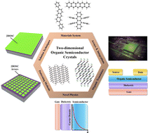
Two-dimensional (2D) organic semiconductor crystals (OSCs) have the advantages of ultrathin thickness, long-range ordered molecular structures, the absence of grain boundaries, and low defect and impurity densities, and they are of great significance for revealing the charge transport mechanism of OFETs, achieving efficient charge injection and transport, and preparing high-performance devices. However, the preparation of large-area high-quality 2DOSCs and investigation of their intrinsic properties remains challenging; especially, fabricating 2DOSC arrays is indispensable for integrated applications. Herein, we first carefully review the solution-processed materials and techniques for fabricating 2DOSCs and 2DOSC arrays because of their low-cost large-area preparation capability. Then, we discuss the novel physical and electronic properties of 2DOSCs at the 2D limit. Furthermore, we summarize recent advances in high-performance OFETs based on 2DOSCs and corresponding heterojunctions. Their device arrays and integrations for practical applications are also highlighted. Finally, the pivotal challenges and future opportunities that include the fundamental investigations and practical application of 2DOSCs are listed. These summaries highlight the scientific significance of this field; can help researchers to improve the efficiency of literature retrieval in this rapidly developing field; provide some references for practical applications; and will attract more researchers, engineers and entrepreneurs with backgrounds in physics, chemistry, materials and microelectronics to join the research and development of 2DOSCs, OFETs, and circuits.
2DOSCs are important members of the 2D material family; they are periodically arranged monolayer or few-molecular-layer organic semiconductors connected by non-covalent interactions (van der Waals (vdW) forces, hydrogen bonds, π–π interactions, dipole–dipole interactions, etc.) on the 2D plane42,43 and have many intriguing features, including the absence of grain boundaries, minimal defects and traps, and high purity. As semiconductive channel materials in electronics and optoelectronics, 2DOSCs have received less attention and research than 2D TMDCs and organic–inorganic hybrid perovskites, which is attributed the lower carrier mobility (slightly lower than 2D hybrid perovskites) and greater contact resistance of 2DOSCs than TMDCs,5,44–51 among other factors. However, 2DOSCs have their own features and advantages, as follows: (i) diverse processing techniques include low-cost and large-area solution methods; (ii) a large material library with structures can be designed and electronic and optoelectronic properties can be easily regulated; and (iii) excellent flexibility and transparency. These unique characteristics and advantages make 2DOSCs not only act as a good complement to 2D TMDCs and hybrid perovskites but also act as potential candidates for next-generation high-performance electronic and optoelectronic devices.52–55 The charge transport of organic field-effect transistors (OFETs) mainly occurs in the monolayer or first few molecular layers of organic semiconductors at the semiconductor/dielectric interface, which is also a key scientific issue in the field of organic electronics.23,56 Therefore, highly ordered 2DOSCs offer perfect platforms for revealing the charge transport mechanism and investigating the intrinsic properties as well as structure–property relationships even with a monolayer or few layers.23,24,56,57 It is reported that the molecular-level thickness in 2DOSCs is smaller than the transport mean free path of many particles including electrons, excitons and phonons, which forces them to follow ballistic transport rather than scattering or diffusion.58,59 2DOSCs and 2DOSC-based transistors demonstrate layer-dependent electronic/optoelectronic properties because of different molecular packing motifs.23,26,56,60–64 Furthermore, 2DOSCs can act as clean and flat platforms for constructing heterojunctions and superlattices, which are helpful to achieve novel physics, diverse device structures, and versatile functions.63,65–68 Mono-/few layer 2DOSCs have excellent optical transparency and they have a dimension far smaller than the wavelength of light, which help achieve lower dark currents and noise,55,69 and thus they are widely used in photodetectors,55,70 organic light-emitting diodes (OLEDs),71 and lasers,72 as well as some special application scenarios such as polarized light detectors,30,31 wide spectrum light detectors,73 and neural network image sensors.67,68 Compared with their bulk OSC counterparts, monolayer and few-molecular-layer 2DOSCs can effectively reduce interlayer charge shielding and facilitate charge carrier injection and transport, which are of great significance for realizing electronic devices with better performance.23,56,57,74 With the continuous synthesis of new materials and the improvement of device preparation processes, as well as the deepening investigations on charge injection and transport mechanisms, 2DOSCs exhibit high field-effect mobility (>10 cm2 V−1 s−1) and low contact resistance (<1000 Ω cm).26,57,60,61,74,75 Accurate positioning of 2DOSCs into specific patterned structures is essential for integrated device applications. Well-patterned 2DOSCs not only reduce leakage current and crosstalk between adjacent devices, but can be easily integrated with other device elements and their corresponding interconnects.42,49,76–78 So far, a lot of organic small-molecules have been prepared into 2D structures, and organic crystal patterns with a 2D morphology have been reported in several researches. However, 2DOSCs are still in their infancy and the fabrication of highly crystalline 2DOSCs and 2DOSC arrays lacks guidance. Hence, reviewing the 2DOSC and 2DOSC array preparation, novel physics, and high-performance devices and their integrations is significant for this rapidly developing field (Scheme 1).
In this review, we firstly summarize the classical solution-processed materials and methods of 2DOSCs and 2DOSC arrays due to their low-cost and large-area processibility, where the growth conditions and mechanisms are discussed carefully (Chapter 2). Then, the packing motifs, intrinsic properties and charge transport mechanisms of 2DOSCs at the 2D limit are reviewed in detail (Chapter 3). Thirdly, the significant advances in high-performance OFETs and integrations or arrays based on 2DOSCs and their corresponding heterojunctions are listed (Chapter 4). Finally, we point out the challenges and future opportunities in the rapidly developing field of 2DOSCs (Chapter 5).
Fig. 1a lists the acene derivatives generally used in preparing 2DOSCs by solution techniques. Pentacene is a typical representative of acene derivatives and the “star” of organic semiconductor materials. Its tight molecular packing and intermolecular interactions give it excellent charge transport performance. The maximum field-effect mobility of pentacene single crystals prepared by the PVT method reached up to 40 cm2 V−1 s−1.99 However, the solubility of pentacene is poor, making it difficult to directly prepare 2DOSC by solution techniques. In this case, indirect solution methods can be used to grow 2D crystals, such as thermal conversion from its precursor solution. The key to this method is to choose a suitable solvent to dissolve the pentacene precursor. The boiling point of the selected solvent should be higher than the conversion temperature of the precursor, and the precursor should have a reasonable solubility in the solvent. Takeya et al. dissolved the precursor of 13,6-N-sulfinylacetamido-pentacene in an ionic liquid (IL) of 1-ethyl-3-methylimidazolium bis(trifluoromethanesulfonyl)imide (emim-TFSI) and the precursor could be converted into pentacene under 120–200 °C.100 The subsequent crystallization and transfer of the single crystal onto the target substrate result in pentacene single crystals with a 2D morphology. The field-effect test showed that their hole mobility was up to 2.1 cm2 V−1 s−1.
Perylene is an isomer of pentacene, which has long π–π stacking distances between molecules, resulting in relatively low mobility. The maximum mobility of 2D perylene single crystals prepared by the solution epitaxy method was 0.18 cm2 V−1 s−1.101 Hu's team designed and synthesized a unique anthracene derivative of 2,6-diphenylanthracene (DPA). The molecular packing motif was head-to-tail J-type aggregation, and high mobility and strong fluorescence emission were obtained. The DPA single crystal prepared by the PVT method had a high mobility of 34 cm2 V−1 s−1 and a high photoluminescence quantum yield of 41.2%.71 The solubility of DPA molecules is very low at room temperature. Hu and Jie's group cooperated and prepared DPA single crystal arrays by the channel-restricted meniscus self-assembly method at higher temperatures (120 °C), and the highest and average field-effect mobility were 39.3 and 30.3 cm2 V−1 s−1, respectively.102 In order to improve the solubility of acene materials, substitution reactions are usually carried out at carbon sites with active hydrogen, and modification at these sites is also beneficial to enhance the stability of materials. For example, 2,6-bis(4-hexylphenyl) anthracene (C6-DPA) has a much higher solubility than DPA, and it's often used in solution preparation of large-area 2DOSC.62,66,101,103,104 The solubility and air stability of 6,13-bis(triisopropylsilylethynyl)pentacene (TIPS–PEN) is greatly enhanced, which can be obtained by substitution at active sites 6 and 13 of pentacene.25,105 The molecular packing motif changes from the herring-bone packing of pentacene to the 2D bricklayer packing of TIPS–PEN, which is more conducive to the formation of a 2D morphology.106
Fig. 1b shows the chalcogenide heterocyclic materials commonly used in growing 2DOSCs through solution strategies. Thiophene is an important class of five membered sulfur-containing heterocycles, which are often used to design and synthesize high-performance soluble p-type organic semiconductor materials. Sulfur atoms in thiophene can provide a pair of lone pair electrons to conjugate with two CC, forming a delocalized large π bond. In addition, sulfur atoms can also produce more weak intermolecular interactions, such as S⋯S and S⋯C interactions, resulting in excellent charge transport performance in thiophen-based materials and facilitating the preparation of 2DOSCs. Hu et al. prepared large-area 2DOSCs based on HTEB molecules by introducing thiophene units into the molecules to generate π–π interactions for efficient solution self-assembly of 2D crystals on various substrates.23 C8-BTBT, one of the leading thiophene-based materials, has a herring-bone stacking on the ab plane while the bc plane belongs to layered stacking since the alkyl chains weaken the interlayer interactions. Intermolecular S⋯S (3.606 Å) and S⋯C (3.468 Å) interactions result in a 2D carrier transport channel which is favorable for charge transport.57,107–109 For example, Hasegawa's group inkjet-printed C8-BTBT single crystal films that showed excellent charge transport performance and the maximum field-effect mobility was 31.3 cm2 V−1 s−1.107 He et al. used the vdW epitaxy method to grow monolayer C8-BTBT single crystal films on the h-BN substrate and the highest field-effect mobility exceeded 30 cm2 V−1 s−1.57
The star molecule of dinaphthalo [2,3-b:2′,3′-f] thiopheno [3,2-b] thiophene (DNTT) and its derivatives in the thiophene-based materials synthesized by Takimiya's team have also received widespread attention and research due to their excellent air stability and remarkable charge transport performance.110 The solubility of DNTT molecules is very poor, so it's not possible to prepare DNTT crystals directly by solution processes. The maximum mobility of 2D DNTT single crystals prepared by Takeya et al. through the thermal conversion of its precursor solution was 2.4 cm2 V−1 s−1.100 Cn-DNTT (n = 6, 8, 10, and 12) can be obtained by modifying DNTT with different alkyl chains, which can improve its solubility to a certain extent.111 Paddy et al. heated the substrate to further improve the solubility of C10-DNTT, and the field-effect mobility of large-area monolayer C10-DNTT crystals prepared by solution shearing reached 10.4 cm2 V−1 s−1.26 Takeya's group synthesized high-performance solution-processable V- and N-shaped molecules with extraordinary thermal stability, including dinaphtho[2,3-b:2′,3′-d]-thiophene (DNT-V)-based and dinaphtho[2,3-d:2′,3′-d′]benzo[1,2-b:4,5-b′]dithiophene (DNBDT)-based materials.112–114 The charge transport performance can be regulated by changing the length and position of the alkyl chains of V-shaped molecules, and the mobility of C10-DNT-VW and C6-DNT-VW single crystal films prepared by the solution method reached 6.5 and 9.5 cm2 V−1 s−1, respectively.112 Alkylated N-shaped molecules of C10-DNBDT-NW had a maximum field-effect mobility of 16 cm2 V−1 s−1 from its single crystalline thin films prepared by the solution edge-casting method.114 Takeya et al. obtained wafer-scale C8-DNBDT-NW crystalline films with controllable layers by optimizing the preparation conditions and used them to prepare a high frequency OFET and rectifier.60 Furan is another kind of important five membered sulfur heterocycle. Because the radius of the oxygen atom is smaller than that of the sulfur atom, the furan-based materials may have a closer molecular packing than the thiophene-based materials. Moreover, furan-based materials have better planarity and solubility than thiophene-based materials, which is conducive to solution processing. Takeya et al. reported stable dinaphtho[2,3-b:2′,3′-d]furan (DNF-V)-based and naphtho[2,1-b:6,5-b′]difuran (NDF)-based molecules, and C10-DNF-VW, C10-DNF-VV and C8-DPNDF are their representatives and the field-effect mobility of their single crystal films prepared by the solution process were 1.1, 1.3 and 3.6 cm2 V−1 s−1, respectively.113,115
Naphthalenediimide (NDI) and perylenediimide (PDI) derivatives are hot topics in the field of n-type organic semiconductor materials. They have strong electron-withdrawing groups of carbonyls, so these molecules have a low LUMO level and good stability, and the position of the nitrogen atom in imide can introduce different kinds of substituents, which is convenient for synthesizing functional materials with diverse physicochemical properties. Govindaraju et al. reported that phenylalanine methylester-functionalized naphthalenediimide (L- and D-NDI) could self-assemble into large-area 2D single crystalline nanosheets (thickness: 10–100 nm, length: ∼100 μm).122 The NDI core undergoes π–π stacking under enhanced hydrophobic interactions, and the balance between hydrophobic and π–π interactions promotes the self-assembly of L-NDI and D-NDI to form 2D single crystalline nanosheets. Compared with NDI, PDI has a larger conjugated plane, which is conducive to the formation of a packing mode with tight intermolecular forces. Takeya et al. prepared large-area and highly crystalline N,N′-1H,1H-perfluorobutyldicyanoperylene carboxydi-imide (PDIF-CN2) thin films through using the edge-casting method. The PDIF-CN2 molecules presented an obvious layered growth mode with the area of a single crystal domain of more than 200 μm2 and the highest field-effect mobility of 1.3 cm2 V−1 s−1.123
The cyano group has a strong electron-withdrawing effect and is often introduced into the molecular skeleton of n-type semiconductor materials. Park et al. reported that dicyanodistyrylbenzene (DCS) derivatives could form a 2D morphology by multiple hydrogen bond networks.124,125 In addition, the unique torsional spring behavior of DCS molecules, i.e., the conformational change from the twisted conformation of the solution state caused by self-assembly to the planar rigid conformation of the tightly stacked solid, provides a powerful impetus for the realization of solution preparation of n-type crystals.124,126 However, simple DCS derivatives can’t obtain a field-effect electron mobility of more than 1 cm2 V−1 s−1 due to their relatively small π-conjugated length. For example, (2Z,2′Z)-3,3′-(1,4-phenylene)bis(2-(3,5-bis(trifluoromethyl)phenyl)acrylonitrile) (CN-TFPA) 2D crystals demonstrated a maximum electron mobility of 0.55 cm2 V−1 s−1.124,126 In order to expand the π conjugated system of DCS derivatives, Park et al. inserted two thiophene rings into the structural framework of DCS and synthesized (1,4-phenylene) bis (2-(thiophen-2-yl) acrylonitrile) (PTA) derivatives.127–129 Among them, (2E,2′E)-3,3′-(2,5-bis(hexyloxy)-1,4-phenylene) bis(2-(5-(4-(trifluoromethyl)phenyl)thiophen-2-yl)acrylonitrile) (Hex-4-TFPTA) showed an electron mobility of up to 2.14 cm2 V−1 s−1 in vacuum deposited films with nanoribbon crystal domains.129 Although Hex-4-TFPTA exhibits excellent charge transport performance, it has poor solubility possibly due to its strong π–π packing and tightly interleaving alkyl chains. To take advantage of the excellent charge transport ability of the Hex-4-TFPTA compound and make it have an ideal solution processing property by structure modification, Park et al. synthesized (2E,2′E)-3,3′-(2,5-dimethoxy-1,4-phenylene) bis (2-(5-(4-(trifluoromethyl)phenyl)thiophen-2-yl)acrylonitrile) (Me-4-TFPTA) molecules by replacing hexyl groups with methyl groups.118 By this structural modification, the crisscross of cyano groups could be alleviated and the formation of a lateral hydrogen bond could be promoted. Me-4-TFPTA molecules have strong self-assembly ability and are easy to prepare by the solution process, and single crystals can be grown by a simple drop-casting method. Interestingly, Me-4-TFPTA molecules can be assembled into diverse morphologies under different solvent conditions. In solvents such as chloroform, 1,2-dichloroethane and toluene, Me-4-TFPTA molecules self-assemble into 1D linear crystals, while in chlorobenzene solvent, Me-4-TFPTA molecules self-assemble into 2D ultrathin nanosheet crystals (3–20 molecular layers with the width of up to hundreds of micrometers and the length of up to submillimeters). Four different hydrogen bond interactions in every molecule greatly promote the crystal growth along the [010] direction (the distance between the edge-to-face pairs of –CN⋯HC– is 2.60 Å). Additionally, chlorobenzene molecules fill the gaps in the 2D nanosheet crystals and generate additional intermolecular interactions (halogen bonds) with the methoxy groups of Me-4-TFPTA along the [010] direction, which may restrict the rotational motion of methoxy groups and guide the hydrogen bonds between cyano-methoxy groups, facilitating lateral self-assembly. In addition, the absence of specific intermolecular interactions along [100] leads to the minimization of crystal growth along the out-of-plane direction, resulting in the formation of ultrathin 2D nanosheet crystals in the drop-cast sample of Me-4-TFPTA. The field-effect mobility of 2D nanosheet single crystals is two orders of magnitude higher than that of 1D single crystals, and the maximum mobility is up to 7.81 cm2 V−1 s−1, which is mainly due to the close contact between the 2D nanosheet structure and electrode and/or dielectric layer. For the purpose of preparing large-area n-type 2DOSCs with a monolayer or few molecular layers, Hu et al. reported 2D single crystals with a maximum size up to millimeters and a thickness of 4.8 nm (2–3 molecular layers) by the solution epitaxy method based on a furan-thiophene quinoidal compound (TFT-CN), and the maximum field-effect electron mobility was 1.36 cm2 V−1 s−1.55 Different from the solid substrate, when the TFT-CN molecular solution is drop-cast on the water surface, it spreads rapidly to the entire water surface under surface tension, and the “coffee-ring”130,131 effect is reduced by eliminating the pinned three-phase contact line, and the nucleation density is decreased due to the larger spreading area than that on the solid substrate. During solvent evaporation, the TFT-CN molecules are self-assembled by intermolecular vdW forces, leading to large-area uniform 2D single crystals. Typically, organic semiconductors grow on SiO2 substrates in a step-like and layer-by-layer mode. In order to produce monolayer crystals, organic semiconductors should have strong molecular interactions and 2D orientation within the intralayer, while weak forces along the interlayer direction are required to inhibit the nucleation and growth of the second layer. Based on the above considerations, Jiang et al. used the conjugated molecule of dicyanomethylene-substituted fused tetrathienoquinoid (CMUT) to prepare large-sized monolayer crystals on polymer substrates by the gravity-assisted 2D spatial limitation strategy and the monolayer crystals obtained on bare SiO2/Si substrates were up to centimeter size.24 Due to the inability to grow large enough CMUT single crystals, they infer the molecular packing of CMUT from the compound of dicyanomethylene-substituted tetrathienoquinoid with hexyl substituents (CMHT), which has the same conjugated core as CMUT and is easy to obtain submillimeter-size large single crystals.132 Similar to CMHT, the non-bonding contact (S⋯N) and the short π–π packing distance of CMUT produce strong 2D intralayer interactions. Compared with CMHT, introducing the branched alkyl chains in CMUT is expected to weaken the interlayer forces by inhibiting the attractive N⋯H interactions along the interlayer direction, and improve the solubility of CMUT in ordinary organic solvents for solution preparation of 2D crystals. Therefore, CMUT can preferentially achieve effective 2D intramolecular stacking to grow large-area monolayer crystals.
C60 is an allotrope of carbon with aromatic properties. Because the spherical molecular structure of C60 is not conducive to the generation of uniform and continuous ordered films, it is necessary to induce the continuous ordered growth of C60 to produce high-quality thin films or crystals. In 2012, Bao et al. reported a droplet-pinned crystallization method to prepare C60 single crystals.133 The working principle of this method is as follows: in the process of droplet drying, the crystal nucleates near the solid–liquid–gas three-phase contact line, the Pinner in the center of the droplet generates a stable receding contact line, and the crystal grows along the receding direction of the droplet (toward the center direction). By using various solvents, C60 single crystals with different morphologies could be prepared, e.g., 1D needles (the solvent is m-xylene), and 2D ribbons (the solvent is a certain proportion of mixed m-xylene and carbon tetrachloride). For 2D ribbon-like C60 single crystals, the presence of solvent molecules (m-xylene and/or carbon tetrachloride) can promote 2D growth of n-type C60 molecules by balancing π–π packing interactions. On the one hand, compared with 1D needle-shaped crystals, 2D ribbon-like crystals have a larger contact area with electrodes and insulators, so the output current of OFETs prepared by 2D ribbon-like crystals is higher. On the other hand, the solvent molecules contained in 2D ribbon-like crystals act as charge traps, which also reduces the field-effect electron mobility.
Blade coating is a scalable preparation method that is commonly employed to deposit polymer films, and it often requires the use of a viscous solution to produce films with a thickness at the micrometer-level.135,136 Solution shearing is a technique derived from blade coating. In 2008, Bao et al. improved the traditional blade coating method, which could be used to deposit a variety of small-molecule semiconductor films with extremely thin, non-viscous and volatile solutions.137 By adjusting the substrate temperature, solution concentration and shearing rate, the thickness, crystallization and uniformity of the deposited films could be optimized. Therefore, the performance of the thin film devices prepared by solution shearing was better than that prepared by drop casting. Thanks to the efforts of the researchers, solution shearing has become a highly versatile coating method, showing great potential in the production of large-area highly oriented organic semiconductor crystalline films.25,60,80,105 Solution shearing usually involves injecting a solution between the blade and the substrate, and due to capillary action, the solution forms a meniscus between the blade and the substrate. The blade and substrate move at a fixed relative speed, and as the meniscus moves and the solvent continuously evaporates, a large-area highly oriented crystalline thin film is ultimately generated on the substrate.138
Bao et al. successfully fabricated a metastable molecular packing structure through the solution shearing method for the first time, known as the “lattice strain” crystal structure.25 Adjusting the intermolecular packing by this method is very important for producing high-performance devices, because reducing the π–π packing distance between molecules can significantly enhance the charge transport.96,139–142 On the foundation of traditional solution shearing, Bao et al. developed a micropillar-patterned blade technique.105 By nano-processing on a blade, a micropillar-patterned blade was obtained and higher quality crystals were acquired via solution shearing. The schematic diagram of the micropillar-patterned blade and scanning electron microscope (SEM) and optical microscope (OM) images are shown in Fig. 2a; solution shearing was carried out by this blade. It can be seen from the fluid dynamics simulation that after the solution passes through the micropillar-patterned blade, the solution is discharged to both sides in the semicircular area. The horizontal velocity is successfully introduced by the micropillar-patterned blade, distinguishing from the vertical velocity along the solution shearing direction (Fig. 2b). The velocity in the horizontal direction leads to better solution mass transport, resulting in higher crystal quality. Polarized optical microscopy (POM) images in Fig. 2c show that, compared with the control group, the micropillar-patterned blade is used to shear the TIPS–PEN single crystal films with millimeter width, centimeter length, highly aligned, and reduced grain boundaries. Finally, the field-effect mobility of TIPS–PEN single crystal films reached 11 cm2 V−1 s−1.
Fig. 2 (a) Schematic of solution shearing by a micropillar-patterned blade (top). SEM image of a micropillar-patterned blade and inset: top view of the micropillars under an OM (down). (b) Velocity distribution in solution shearing. (c) POM images of TIPS–PEN film by solution shearing, with (left) and without (right) micropillar-patterned blade. Adapted with permission from ref. 105, copyright 2013 Springer Nature. |
The problem of insufficient solution supply will occur when the crystal size exceeds the centimeter-level during solution shearing due to the limited amount of solution between the blade and the substrate, which becomes an important factor that restricts the further growth of crystals. To overcome this difficulty, Takeya et al. developed a solution shearing technique with continuous solution supply function.60,143–145 As shown in Fig. 3a, a steady solution supply is maintained throughout the shearing process by using a blade perpendicular to the substrate and introducing a continuous solution supply pipeline into the blade. This not only helps to provide a continuous material supply for growing large-area crystals, but also helps to maintain a stable meniscus during shearing, leading to improved crystal quality and uniformity. Through this method, they prepared wafer-scale crystalline thin films and achieved functions similar to controlled layer numbers (Fig. 3b). The field-effect mobility of bilayer C8-DNBDT-NW single crystals was 13 cm2 V−1 s−1, the contact resistance was 46.9 Ω cm, and the cut-off frequency was 20 MHz, which laid a solid foundation for the realization of high-speed organic circuits.60
Fig. 3 (a) Schematic diagram of continuous solution supply solution shearing equipment. (b) Combined SEM image of an ultrathin monolayer and bilayer single-crystalline film. Adapted with permission from ref. 60, copyright 2018 AAAS. (c) Principle of monolayer crystal growth by dual solution shearing. Adapted with permission from ref. 26, copyright 2017 Wiley-VCH. |
As for the fabrication of monolayer 2DOSC by solution shearing, Paddy et al. made an important breakthrough and successfully prepared millimeter-sized monolayer C10-DNTT single crystals by dual solution shearing.26 As shown in Fig. 3c, in the first solution shearing, a multilayer heterogeneous organic crystalline film was formed. In the second solution shearing, the substrate temperature was slightly higher than that in the first shearing, so the solvent could dissolve more C10-DNTT molecules. Due to the weak adhesion work (50.0 mN m−1) between C10-DNTT molecules, the upper layer of C10-DNTT molecules would preferentially dissolve and fill the areas not covered by the underlying layer molecules. In addition, strong adhesion (64.3 mN m−1) exists between the underlying molecules and the substrate, which alleviates the dissolution process in comparison with other layers. Therefore, by precisely regulating the substrate temperature and solution concentration, and taking advantage of the differences in adhesion between C10-DNTT molecules as well as between C10-DNTT molecules and substrate, the dual solution shearing could produce large-area monolayer organic crystals.
The solution shearing method is also commonly referred to as “bar coating” when cylindrical or rectangular bars are used as blades. The bar is in close contact with the substrate surface during bar coating, so the meniscus is usually confined to a small space, which induces geometric confinement to prevent molecular stacking misalignment. Although the bar coating method has this advantage, there are few reports on using it to deposit small-molecule organic semiconductor films. Through finite element modeling and experimental study, Paddy et al. demonstrated that the flow caused by temperature-dependent surface tension gradient near the meniscus had a negative impact on deposited crystals and their electrical properties.146 They used different solvent combinations to control the concentration-dependent surface tension gradient near the meniscus to balance temperature-induced Marangoni flow with concentration-induced Marangoni flow and enhance the mass transport of organic semiconductor molecules to the contact-line region. They eventually prepared large-area highly crystalline C8-BTBT thin films through bar coating and the average and maximum mobilities of OFETs were 13.7 and 16 cm2 V−1 s−1.
MGC techniques are low-cost, high-throughput and large-area deposition methods for producing organic semiconductor crystalline films. Although MGC techniques have made progress in controlling the morphology, molecular stacking, and crystal orientation of organic semiconductor thin films, there are still many challenges that need to be addressed, mainly including the following three points. (i) High deposition rates (>17 mm s−1) and low temperatures (such as environmental conditions) are necessary to achieve low-cost mass-production.147 However, the deposition rates for high-quality organic semiconductor thin films of MGC techniques usually are low (<1 mm s−1) and the substrates commonly require to be heated. From the perspective of organic semiconductor growth kinetics, rapid crystallization at low temperature generally leads to low crystallinity, high defect density and small grain size, which reduces the charge transport efficiency of organic semiconductor films. Therefore, fast deposition of high-quality films at room temperature remains a key challenge. (ii) Organic semiconductors have excellent intrinsic flexibility and are naturally suitable for flexible device applications.148,149 However, MGC techniques are difficult to fabricate high-quality organic semiconductor films on flexible substrates, and their deposition process may be limited by the rough and non-wetting surfaces, processing temperature, and incompatibility with solvents, which means that the MGC methods have more stringent requirements for preparing high-quality films on flexible substrates. (iii) Currently, MGC techniques can achieve the preparation of wafer-scale crystalline thin films, but MGC techniques are difficult to completely eliminate the grain boundaries, so it is hard to realize the production of wafer-scale single crystalline domains.26,105,143
In 2011, Hu et al. prepared millimeter-sized 2D HTEB crystals by the drop casting method.23 The HTEB molecule has several characteristics: (i) thiophene units are introduced to generate π–π interactions and realize efficient self-assembly; (ii) the introduction of triple bonds in the molecule prevents the rotation of adjacent rings; and (iii) alkyl chains are introduced into the molecule to improve solubility and assist crystallization. HTEB molecules can efficiently assemble into large-area 2D crystals on a variety of substrates by a simple drop casting method. The atomic force microscope (AFM) image in Fig. 4a shows that the edge step-height is 3.5 nm, which corresponds to the monolayer thickness. Fig. 4b demonstrates that the film in different regions has consistent selected area electron diffraction (SAED) patterns, indicating that the entire film is a single crystal.
Fig. 4 (a) AFM image of HTEB crystals with a thickness of 3.5 nm, the scale bar is 2.5 μm. (b) SAED patterns of 2D HTEB crystal. Adapted with permission from ref. 23, copyright 2011, Wiley-VCH. (c) Molecular structure of fullerene derivatives and AFM image of 2D crystals formed by derivatives. (d) Bright-field TEM image of 2D crystals. Inset: SAED pattern from monolayer 2D crystals. Adapted with permission from ref. 150, copyright 2015, Wiley-VCH. (e) Schematic representations of geometrical models and chemical compounds for the space-filling design method. Adapted with permission from ref. 151, copyright 2015, AAAS. |
Zhu's group designed and synthesized a series of C60-based liquid crystalline materials to grow 2D crystals.150 The proposed strategy is to modify long alkyl chains onto C60 molecules (Fig. 4c), and the molecules will self-assemble to form 2D layered crystals owing to the π–π interactions between C60 molecules and the phase separation between C60 molecules and alkyl chains. Fig. 4c exhibits that the lateral size of 2D crystals is several micrometers and the thickness is 5–6 nm. Bright-field transmission electron microscopy (TEM) images show a clear layer-by-layer growth motif, indicating the 2D property of the crystals (Fig. 4d). Fukushima et al. reported a “space filling” design strategy that relies on 2D nested hexagonal stacking of a special class of triptycene molecules.151 As shown in Fig. 4e, the propeller-shaped triptycene molecule is composed of three 120°-oriented phenylene rings, which self-assembles into a 2D hexagonal structure through nested stacking. The hexagonal structure has the geometric constraint of vertex displacement and avoids the translation disorder in plane. The alkanes of triptycene provide molecular fluidity to facilitate the reordering of the resulting assembly. In the “2D (hexagonal, 2D in-plane packing) + 1D (layered, 1D out-of-plane packing)” structure, the molecules can’t move freely and can only be arranged in a specific order. Through simple vacuum evaporation, spin coating and cooling from isotropic liquid, a large-area perfectly oriented molecular film can be produced. Subsequently, Fukushima et al. found that triptycene with excellent self-assembly ability could be employed as a supramolecular scaffold to tailor functional molecular units into 2D structures.152 The C60 unit was used to alter the triptycene skeleton and then resoundingly assembled into a highly oriented 2D hexagonal morphology. Jiang et al. prepared large-area monolayer crystals by bottom-up growth, which depends on particular CMUT molecules with strong intermolecular interactions in plane and weak forces in intralayer.24 They drop-cast CMUT solution onto a hydrophobic substrate at the bottom and then covered the top with a hydrophilic substrate. As the solvent evaporated, a very thin solution layer was formed in the 2D space between the two substrates with the assistance of gravity from the top substrate, resulting in large-area monolayer crystals on the top hydrophilic substrate after the complete volatilization of the solvent.
The preparation of large-area 2D crystals by simple drop casting or spin coating requires rigid design of molecular structures to make them have strong solution self-assembly ability, and currently few molecules have been reported. The introduction of insulating alkyl chains into molecules can reduce their semiconductor properties, for example, 2D crystals of HTEB, CMUT, and pyrazine-fused derivative70 demonstrate relatively low field-effect mobility (∼1 cm2 V−1 s−1). Therefore, it is vital to seek a balance between the π-conjugated core and alkyl chains through rational molecular design for taking into account both the charge transport ability and the solution self-assembly capability of organic semiconductor molecules. In addition, the 2D single crystals prepared by drop casting or spin coating methods are limited to sub-millimeter and millimeter sizes. Although the centimeter-sized n-type 2D CMUT crystals can be obtained on the hydrophilic Si/SiO2 substrate, it will lead to the degradation of device performance. Hence, there is an urgent requirement to develop universal growth methods and design high-performance molecules with strong self-assembly ability to produce large-area single crystalline thin films on various target substrates.
N = N0e−L/Gt | (1) |
Nucleation density can be controlled by adjusting the nucleation barrier and the supersaturation concentration. The relationship between the total Gibbs free energy of heterogeneous nucleation (ΔGhetero) and the total Gibbs free energy of homogeneous nucleation (ΔGhomo) can be expressed by eqn (2):156
ΔGhetero = ΔGhomo × f(θ) | (2) |
f(θ) = [(2 + cosθ) (1 − cosθ)2]/4 | (3) |
Fig. 5 (a) Schematic diagrams of 2DOSCs grown by solution epitaxy. (b) OM image of centimeter-sized perylene 2DOSCs (blue), inset: molecular structure of perylene and XRD and SAED pattern of perylene 2DOSCs. Adapted with permission from ref. 101, copyright 2016, Wiley-VCH. |
Solution epitaxy offers a simple and effective method for the preparation of large-area organic crystals, and detailed investigations of this process further improve the quality of organic crystals. For instance, considering the spread of organic semiconductor solution on the water surface, the spreading coefficient S = γ1 − γ2 − γ12, where γ1, γ2 and γ12 are the surface tensions of water, solution and solution/water interface, respectively. Better spread of organic solutions at the water surface results in fewer nucleation sites, which is especially crucial for organic solvents that are heavier than water, such as chlorobenzene, which spread poorly. Li et al. found that partial wetting and negative spreading coefficient (S < 0) leads to the formation of a compact float lens, producing three-dimensional (3D) crystals rather than 2D crystals after total evaporation of the solvent.158 When the surfactant is added into water, γ12 is greatly reduced, which enhances the spreading area of the organic semiconductor solution (the solvent is chlorobenzene) on the water surface by more than 20 times, and thus the ideal spatial-limited growth pattern of 2D crystals is required (Fig. 6a). Under suitable surfactant concentrations (≤ 10 mg mL−1), the maximum areas of the resulting crystals increase linearly with the enhanced surfactant concentrations, as shown in Fig. 6b. XRD and SAED data confirm that the prepared films are single crystals. Li et al. further developed this method by replacing water with glycerol–water mixed solution or pure glycerol.62 Compared with water, glycerol has a higher critical micellar concentration. Therefore, as the glycerol concentration increases, surfactant molecules are more likely to accumulate at the interface between the organic solution and the glycerol–water mixture, leading to an effective decrease in γ12, thereby increasing the spreading area and facilitating the assembly of 2D crystals. In addition, glycerol has a high viscosity, and thus solution viscosity increases with increasing glycerol concentration, promoting stable floating of the organic solution and allowing more precise control of the growth process of organic crystals and molecular layer numbers. As shown in Fig. 6c, a surfactant and a certain amount of C6-DPA solution were added into the glycerol–water mixed solution and the spreading area was controlled by the glycerol/water ratio. Finally, multilayer to bilayer controllable C6-DPA single crystal films were obtained by this method, and the maximum size of monolayer crystals could reach up to centimeters.
Fig. 6 (a) Schematic diagrams of 2DOSCs grown by the water surface space-confined method. (b) Maximal crystal area as a function of the concentration of the surfactant. Adapted with permission from ref. 158, copyright 2018, ACS. (c) The average layer number of 2DOSCs as a function of the volume fraction of glycerol in the water-glycerol mixed liquid substrate. Adapted with permission from ref. 62, copyright 2019, Wiley-VCH. |
Changing the solvent is another efficient method to design the spreading coefficient. As shown in Fig. 7a, Jie's group used various solvents to tune γ2, and finally obtained centimeter-sized C10-BTBT single crystal thin films by the external-force-driven solution epitaxy method.159 They found that the spread of organic semiconductor solution was poor (S < 0) when chlorobenzene solvent was used, resulting in the formation of 3D crystals. On the other hand, if the surface tension of the solvent was much less than the surface tension of water (e.g., ethyl acetate), the solution spread too quickly after dropping (S > 0), and C10-BTBT molecules didn’t have enough time to grow into continuous 2D single crystal films, leading to some small sheet crystals randomly dispersed on the water surface. Only when dichloromethane solvent was used, the solution could be spread on the water surface (S > 0), and C10-BTBT molecules had sufficient time to grow into large-area 2D single crystals. Although large-area and layer-controlled organic crystal films are obtained, controlling crystal orientation is also considerable for improving device performance. The formation of organic crystals on the water surface depends on π–π interactions between molecules and leads to arbitrary orientation of crystals. By applying materials with π–π interactions with organic semiconductor molecules on the water surface, the crystallization behavior of organic semiconductors can be altered. Jie et al. reported a centimeter-sized orientation-homogeneous monolayer organic crystal by growing crystals on (GQDs) modified water surface.160 GQDs not only enhance the spreading area of organic solution in a controlled manner, but also reduce the nuclear barrier of organic molecules through π–π interactions. The strong cohesion between GQDs and organic molecules binds organic crystals together to generate large-area crystals. The evaporation of organic solvents can also be controlled by changing the water surface without introducing additives. Recently, Jie et al. demonstrated a new drag-coating method on the water surface for growing high-quality organic crystals with uniform orientation.161 As shown in Fig. 7b, the organic solution was first spread rapidly onto the water surface and then temporarily blocked by the sacrificial thin film. Subsequently, the sacrificial membrane was dragged with a thin glass rod to spread the organic solution onto the water surface again. The high surface tension of water leads to a “constant contact radius” pattern of solvent evaporation, which helps to reduce the grain boundaries of organic semiconductor films and improve crystal quality. At the same time, the drag of the sacrificial film enables the continuous growth of organic crystals in an equilibrium state, producing a large-area organic crystal film with uniform orientation. It proves that introducing directional driving force can effectively achieve consistent crystal orientation when growing crystals on the water surface.
Fig. 7 (a) Schematic diagrams of 2DOSCs grown by external-force-driven solution epitaxy. Adapted with permission from ref. 159, copyright 2019, Tsinghua University Press and Springer Nature. (b) Schematic diagrams of 2DOSCs grown by water surface drag-coating. Adapted with permission from ref. 161, copyright 2021, Wiley-VCH. |
Thanks to the efforts of researchers, many surface energy-controlled solution methods have been developed to grow large-area 2D crystals, including solution epitaxy, 2D space-confined assembly, external-force-driven solution epitaxy, GQD induced self-assembly and water surface drag-coating. These methods are capable of producing high-quality, large-area, layer-controllable, and highly oriented organic crystal films, but this is a relatively time-consuming process due to the slow solvent evaporation rate. Although 2D crystals can be transferred onto a diversity of substrates, which is also conducive to the construction of heterostructures and superlattices, carefully handling nanoscale organic films is also the key to avoid crystal damage. Technical improvements are helpful to future progress, such as vibration isolation and mechanical automation transfer equipment, especially for large-area organic crystals and device integration. In addition, although the introduction of surfactants is useful for the preparation of large-area 2D crystals, the surfactants remaining in the crystals can also lead to the degradation of device performance. Seeking a balance point or using novel surfactants may be the key to further development.
By using suitable patterning strategies to copy the shape of the PDMS template, OSC patterns are successfully prepared. Usually, linear OSC patterns are presented in the literature since capillary force is used for guiding the self-assembly of organic semiconductor molecules in the microstructures of the PDMS mold. For example, the researchers reported these methods—an abrupt heating technique and then combined with a lift-off process,168 capillary force lithography,169 liquid-bridge-mediated nanotransfer molding,170 template-assisted self-assembly,171 and solvent-annealing effect.172 Through optimizing the fabrication methods, some reports have achieved 2DOSC patterns with tunable shapes and sizes.103,173 For instance, Bae et al. demonstrated a selective contact evaporation printing (SCEP) technique to prepare 2D TIPS–PEN crystal patterns with tailored shapes and sizes.173 The patterning process is shown in Fig. 8a. First, the pre-defined PDMS mold was in conformal contact with a large-area flat TIPS–PEN crystalline film under an appropriate pressure (3 kPa), where the TIPS–PEN crystalline film was prepared by controlling the evaporation process of a mixed-solution of toluene/dodecane (50 wt%/50 wt%) on a silicon substrate. Then, TIPS–PEN molecules were selectively evaporated and diffused into the PDMS template at the TIPS–PEN/PDMS interface at a proper temperature (100 °C), leaving well-defined periodically linear TIPS–PEN crystal patterns. Finally, another PDMS template was used to further SCEP TIPS–PEN crystal patterns, allowing for tailoring the crystal patterns with different shapes and sizes at an improved resolution. Fig. 8b and c show the 50 × 10 μm2 rectangular crystal patterns with smooth and uniform edge surfaces, and the film thickness is about 75 nm. By using different PDMS templates, various TIPS–PEN crystal patterns with different symmetries are also obtained, such as square holes arranged in p4mm symmetry and hexagons arranged in p6mm symmetry (Fig. 8d and e). This study demonstrated that the PDMS template-assisted SCEP technique can precisely tailor 2D TIPS–PEN crystals into desired micropatterns with tunable shapes and sizes under adequate conditions, and this method may be applied to other organic semiconductor crystalline films. Further control of crystal thickness and improvement of crystal quality will help promote the application of PDMS templates in patterning 2DOSC. Recently, Chen et al. fabricated high-resolution layer-controlled 2D organic single crystal arrays by combining the solution-processed organic semiconductor engineering strategy and PDMS mold-assisted SCEP technique.103 There are several key points in growing large-area layer-controllable 2D organic single crystals at the air–liquid interface. The preparation of 2D crystals through the solution self-assembly strategy requires that organic semiconductors have strong intralayer interactions and weak interlayer interactions, while organic semiconductors are connected together through weak non-covalent interactions, which leads to the widespread existence of vdW forces along the three axes in 2D organic crystals, and it is difficult to promote the growth of the x and y axes and limit the growth of the z axis. Therefore, selecting appropriate organic semiconductor molecules is crucial for growing 2D single crystals with controllable layer numbers. In this article, the authors selected C6-DPA molecules for growing large-area layer-controlled 2D single crystals. C6-DPA has a large delocalized conjugation π system, which is conducive to self-assembly into 2D crystals through strong intermolecular π–π interactions. C6-DPA also has long alkyl chains, which are beneficial for weakening interlayer interactions and assembling 2D crystals in the plane. In addition, it has a 2D force network and tends to be assembled into a 2D morphology. Moreover, using highly viscous glycerol as a liquid substrate can promote the stable floating of organic solutions and reduce the interference of external environmental factors in the crystal growth process, which helps to control the layer numbers of C6-DPA crystals. Furthermore, by adding phosphatidylcholine to increase the spreading area, the C6-DPA solution forms an extremely thin solution layer on the glycerol surface and C6-DPA molecules are self-assembled in 2D space and the concentration of C6-DPA solution and crystal growth temperature are precisely controlled, and thus large-area layer-controlled 2D C6-DPA single crystals are successfully obtained. Each micropattern in the 2D single crystal arrays is highly consistent in terms of thickness, molecular arrangement, and crystal quality; therefore, the OFET arrays have excellent electrical performance and uniformity. The high-resolution layer-controllable 2D organic single crystal arrays are helpful to investigate the electrical/optoelectronic properties related to layer numbers and improve the uniformity of device arrays. The average mobility of device arrays based on bilayer C6-DPA single crystal arrays is 1.6 cm2 V−1 s−1, and the relative variation is only 12.5%. These results demonstrate that high-resolution layer-controlled 2D organic single crystal arrays are ideal systems for advanced optoelectronics and device integrations.
Fig. 8 (a) Schematic diagrams of the selective contact evaporation printing process. (b) A SEM image of rectangular TIPS-pentacene domains with a width and length of 20 and 50 μm, respectively. The magnified image in the inset displays the smooth edge of a microdomain. (c) An AFM image in height contrast of the rectangular domains shown in (b). (d) Square holes arrayed in p4mm symmetry. (e) Hexagons arranged in p6mm symmetry. Adapted with permission from ref. 173, copyright 2011, Wiley-VCH. (f) Schematic diagrams of the capillary bridge lithography technique for fabrication of 1D organic single-crystal arrays. (g) Low magnification fluorescent image of 1D organic arrays (left), and cross-polarized fluorescence image of 1D organic single-crystal arrays (right). (h) Dark-field fluorescence image of microring arrays. Adapted with permission from ref. 174, copyright 2017, Wiley-VCH. |
Another common template is the silicon template with periodic micropillar-structures developed by Wu et al.72,174–177 They developed several methods to guide organic molecule self-assembly into highly aligned and crystalline arrays, for example, the capillary-bridge lithography strategy,174 PVT guided method,175 3D dewetting mediated assembly,176 liquid knife approach,72 and nano-confined crystallization route.177 Similar to the PDMS templates, 1D linear crystal arrays are usually manufactured because capillary force is often used to guide the self-assembly of organic molecules in the silicon templates. Fig. 8f shows the patterning process for fabricating 1,4-dimethoxy-2,5-di(4-(methylthio)styryl)benzene (TDSB) crystal arrays by capillary-bridge lithography.174 First, a thin organic solution layer was sandwiched between the linear micropillar-structured silicon template and target substrate. The hydrophobic property of sidewalls inhibited the sidewalls from wetting and kept the organic solution suspended on the tops of micropillars since the silicon template was modified with asymmetric wettability, where the sidewalls and tops of micropillars were lyophobic and lyophilic, respectively. Then, the thin organic solution layer underwent fracture as the organic solvent evaporated, forming independent microscale capillary bridges anchored on the micropillars. The micropillar structures determine the position, geometric shape, and size of capillary bridges, thus allowing the production of organic arrays. Last, the TDSB molecules reached supersaturation and crystalized and formed 1D single crystalline arrays at the three-phase contact line of the target substrate after complete dewetting of the capillary bridges (Fig. 8g). Circle-annular TDSB single crystal arrays are also obtained by applying different silicon templates (Fig. 8h). On the basis of an asymmetric-wettability-modified square-shaped micropillar-patterned silicon template, Wu et al. developed a “liquid knife” strategy to fabricate 2D single-crystalline perovskite microplate patterns with a thickness of 900 ± 100 nm.72 Therefore, it is promising that the micropillar-patterned silicon template can be utilized to fabricate 2D organic crystal arrays. Recently, Zhang et al. used the capillary bridge lithography technique to fabricate 1D TFT-CN single crystal arrays by using a micropillar-structured silicon mold with similar asymmetric wettability, and the OFETs demonstrated a high electron mobility of up to 9.82 cm2 V−1 s−1.178 In addition, they also obtained 2D morphologic TFT-CN single crystal arrays with tunable shapes and sizes. However, the thickness of these crystals still far exceeds 100 nm. In OFETs, large crystal thickness is not conducive to carrier injection and also leads to large contact resistance, which reduces device performance. Hence, the preparation of 2DOSC patterns using micropillar-structured silicon templates requires further optimizing solution fabrication conditions to realize ultrathin arrays and expand their application potential.
Fig. 9 (a) Illustration of defined micropattern with a nucleation control region and growth control region. Adapted with permission from ref. 182, copyright 2012, Wiley-VCH. (b) Schematic process of the CONNECT method. Adapted with permission from ref. 77, copyright 2015 Charlesworth. (c) Schematic illustrations of the double-blade coating technique for patterning OSC arrays. (d) POM image of a 5 × 8 C8-BTBT crystal arrays and the ratio of single domain is 62.5%, where ①–③ represent the number of domains for each C8-BTBT crystal patterns. Adapted with permission from ref. 183, copyright 2023, Wiley-VCH. |
In recent years, printing techniques including inkjet printing,184,185 screen printing,186,187 and spray printing188,189 have attracted intensive attention and interest in patterning organic semiconductors with good resolution. However, due to the difficulty in controlling the nucleation and growth of organic semiconductor molecules and the complex drying kinetics, these printing techniques encounter many challenges in preparing organic crystal arrays. It is an effective way to fabricate organic crystal arrays by modifying the substrate with asymmetric wettability and combining with printing methods. Hasegawa et al. demonstrated the preparation of C8-BTBT crystal arrays on an asymmetric wetting patterned substrate by combining inkjet printing and antisolvent crystallization.107 The patterning process is shown in Fig. 10a. First, a drop of antisolvent was printed on the pre-patterned wetting region. Then, a drop of C8-BTBT solution was overprinted onto the top of antisolvent. Third, antisolvent crystallization was used to control nucleation and subsequent crystal growth until a large crystalline film eventually covered the overall surface of antisolvent after solvent evaporation. The key point is that the wetting region contains a protuberance, which effectively positions the seed crystals in the protrusive region during the initial period of thin film formation and induces the seed crystal to grow from the protrusive region to the other end of the droplet.
Fig. 10 (a) Illustrations of combining inkjet printing and antisolvent crystallization techniques. (b) OM images of inkjet-printed 7 × 20 C8-BTBT crystal arrays. (c) POM images of an individual C8-BTBT pattern with the single domain property. Adapted with permission from ref. 107, copyright 2011 Springer Nature. (d) Schematic diagrams of the CRMS method. (e) POM image of the highly aligned DPA crystal arrays. Adapted with permission from ref. 102, copyright 2019 Elsevier. (f) Schematic diagrams of the crystallization process of channel-restricted screen-printing strategy. (g) OM image of a screen-printed crystalline C8-BTBT pattern with PVP banks. (h) POM image of a screen-printed crystalline C8-BTBT pattern with PVP banks. (i) OM image of 8 × 8 C8-BTBT crystalline film arrays on a 3 × 3 cm2 SiO2 substrate. Adapted with permission from ref. 186, copyright 2019 Wiley-VCH. |
Finally, 30–200 nm C8-BTBT crystalline film arrays were acquired on the pre-patterned substrate after the complete evaporation of antisolvent (Fig. 10b). By optimizing printing conditions, C8-BTBT single-crystalline films (Fig. 10c) could be obtained and a maximum field-effect mobility of 31.3 cm2 V−1 s−1 was achieved. In future research, it is necessary to further control crystal thickness and improve crystal quality and pattern resolution to achieve high-performance high-density device arrays and integrated applications. Modifying substrates with 3D bank structures (e.g., insulating polymers and photoresists) and combining with printing techniques is another efficient method to produce OSC patterns. The 3D bank structures can controllably guide the nucleation and crystallization process of organic semiconductor molecules, resulting in the formation of highly crystalline OSC arrays. Photolithography and printing methods can be used to prepare the 3D bank structures. For example, Deng et al. developed a channel-restricted meniscus self-assembly (CRMS) method to produce highly uniform organic single crystal arrays through microscale photoresist channels to control the meniscus front during dip coating.102 As shown in Fig. 10d, the width and shape of the meniscus is effectively confined by the friction/viscous force between the photoresist channels and organic solution. The micro-confinement effect can rationally regulate the evaporation and convective flow of organic solution in the PR stripes, enabling uniform nucleation at the meniscus front. Moreover, the dip coating process guarantees consistent molecular packing of organic single crystal arrays because it can guide the monodirectional motion of the meniscus. By using DPA as a model material, wafer-scale homogeneous organic single crystal arrays are successfully demonstrated. The DPA single crystal arrays have high uniformity in terms of morphology, quality, and growth orientation. As demonstrated in Fig. 10e, all DPA single crystals are highly aligned along the photoresist stripes, and they have very small thickness and width variations (10%). The CRMS strategy ensures DPA single crystal arrays’ highly uniform electrical performance by controlling the nucleation and growth of DPA crystals at the meniscus front and inducing consistent crystal orientation via the dip coating process, and simultaneously defines the spatial resolution of crystal arrays through regulating the size and shape of photoresist channels. To further develop all-printed organic crystal arrays, Duan et al. reported a channel-restricted screen-printing method to produce highly crystalline organic semiconductor thin film arrays by introducing 3D poly(4-vinylphenol) (PVP) banks to control the morphology and crystallinity of small-molecule organic semiconductors.186 The PVP banks have two main effects. One is partially restricting the printed organic semiconductor solution, which can control the shape of organic patterns, and decrease the thickness of the organic semiconductor film by allowing the printing of organic solution with lower viscosity than that of normal screen printing. Another is providing a confinement effect for crystal growth and inducing the directional growth of crystals. As demonstrated in Fig. 10f, the outward convective flow at the two sides of the PVP banks is triggered by the fast solvent evaporation because of the smaller contact angle. Fig. 10g and h shows that the crystallization process starts from the two sides, meets in the middle of the pattern and then stops, and leaves a disruption line. The PVP banks can effectively improve the crystalline quality of the organic semiconductor thin films and the electrical performance of OFET arrays, although obvious grain boundaries are preserved within each pattern. This method demonstrates scalable fabrication ability (Fig. 10i), and it is also compatible with flexible substrates. Later, Duan et al. selectively etched solution-sheared large-area highly crystalline organic semiconductor films to produce 2DOSC arrays by pre-depositing a poly(vinyl alcohol) (PVA) resist layer with the assistance of screen printing.80 The solution-sheared film thickness (4–40 nm) can be adjusted by controlling the ink concentrations. PVA can act as a surfactant, which enhances the wetting ability and adhesion of PVA aqueous solution on organic crystalline films and induces a pinned three-phase contact line during the drying process. Furthermore, the printing of an aqueous PVA protective layer and subsequential selective etching process produces negligible damage to the underlying organic crystalline films. Therefore, the prepared highly aligned 2DOSC arrays demonstrated good electrical performance and uniformity. Taking C8-BTBT as an example, the maximum and average mobility were 8.7 and 6.4 cm2 V−1 s−1 in 40 OFETs, respectively. This combinative strategy provides a powerful approach for achieving high-performance printed flexible devices and circuits.
For the purpose of exploiting the photolithography techniques to fabricate micro- and nanoscale organic semiconductor patterns, researchers have devoted hard work and dedication and explored some alternative strategies, mainly including preparing protective layers between organic semiconductors and photoresists,190–192 and synthesizing robust enough organic semiconductors or modifying existing organic semiconductors to maintain stable states under the standard photolithography processes.193,194 For example, Zakhidov et al. used the orthogonality between organic semiconductors and highly fluorinated photoresists (semi-perfluoroalkyl resorcinarene) to pattern organic semiconductors and prepared micro- and nanoscale OFETs with moderate performance.195 Representative pentacene and poly(3-hexylthiophene) (P3HT) film transistors demonstrated hole mobilities of 0.45 and 2 × 10⁻⁴ cm2 V−1 s−1 with channel lengths of 1 μm (Fig. 11a) and 200 nm, respectively. This work indicates that the orthogonal photoresist is an effective method for photolithography patterning of organic semiconductors to achieve the fabrication of fairly sophisticated organic electronic devices and circuits (Fig. 11b). Paddy's team patterned the bilayer C10-DNTT single crystal for OFET arrays with photolithography techniques by using an orthogonal photoresist (OSCoR 5001).196 As a result, the 4 × 4 OFET arrays on the AlOx gate dielectric (Fig. 11c) presented satisfactory device performance with a mean mobility of 5.1 cm2 V−1 s−1 and a small standard deviation of 0.7 cm2 V−1 s−1, indicating that the multiple photolithography and etching steps didn’t damage the organic crystals. Takeya and co-workers used the orthogonal photoresist of OScOR2312 to fabricate top-contact electrodes on p-type C10-DNBDT and n-type perylene derivative (GSID104031-1) crystalline films, and the field-effect mobility was 3.0 and 0.22 cm2 V−1 s−1 for representative p- and n-type transistors, respectively.197 Later, Takeya's group used an orthogonal fluorine photoresist (OSCoR 4000) to prepare p- (C10-DNBDT-NW) and n-type (GSID104031-1) transistor arrays, and the average mobility was 4.9 and 0.16 cm2 V−1 s−1 for 24 p-type and 24 n-type transistors based on single crystalline films, respectively.198 Furthermore, the complex CMOS circuits were also successfully demonstrated (Fig. 11d). In addition to developing orthogonal photoresists, researchers also explored other feasible routes to pattern organic semiconductors by photolithography techniques, such as modifying organic semiconductors and imparting orthogonality to them.199,200 Park et al. imparted chemical and physical orthogonality to different polymer semiconductor gel films through forming semi-interpenetrating diphasic polymer networks between polymer semiconductors and bridged polysilsesquioxanes (Fig. 11e), and thus the polymer semiconductor gel films could sustain stability after multiple chemical and physical etching steps during photolithography and eventually produce high-resolution patterns.199 This strategy allows the fabrication of various polymer semiconductor patterns at the nanoscale on a single substrate without degrading their optoelectronic properties for achieving CMOS inverters and pixelated polymer light-emitting diodes (Fig. 11f). However, this method may not apply to organic small-molecule semiconductors because it's very challenging to impart orthogonality to them.
Fig. 11 (a) AFM image of a photolithographic pentacene transistor with a channel length of 1 μm. (b) OM image of a ring oscillator based on the top contact pentacene transistor with 1 μm channel length. Adapted with permission from ref. 195, copyright 2011, RSC. (c) POM image of 4 × 4 C10-DNTT transistor arrays on an AlOx gate dielectric. Adapted with permission from ref. 196, copyright 2020 Wiley-VCH. (d) Photography of the CMOS circuits constructed by p- and n-type transistors. Adapted with permission from ref. 198, copyright 2017, Wiley-VCH. (e) Illustration of OPSG films composed of polymer semiconductors interpenetrated into BPSQ networks. (f) Fluorescence microscopy image of patterned pixels of light-emitting OPSG films. Adapted with permission from ref. 199, copyright 2019, Wiley-VCH. |
The above three classes of methods have their own advantages and limitations in patterning organic semiconductors. Table 1 summarizes them to make a clearer comparison and show their scope of application. Depending on the applicable scenarios, selecting the suitable materials and patterning strategies and further improving the performance and uniformity of device arrays will help propel 2DOSCs from single or a small number of devices to medium-scale integrated circuits.
Methods | Conditions | Key techniques | Pattern features (crystal quality, size, shape, resolution, thickness) | Limitations | Demonstrated applications |
---|---|---|---|---|---|
Template-based patterning | PDMS templates: bottom-up self-assembly of organic molecules and top-down fabrication with photo-lithographic templates | Abrupt heating technique combined with a lift-off process | Single- or polycrystalline, tunable sizes and shapes (commonly are linear patterns), resolution: few-micrometer, thickness: tens to hundreds of nanometers | The crystal quality, pattern resolution, and reproduction accuracy (fuzzy edge of patterns, doesn’t match the template exactly) are not high, uncontrollable thickness | OFET arrays |
Capillary force lithography | |||||
Liquid-bridge-mediated nanotransfer molding | |||||
Template-assisted self-assembly | |||||
Solvent vapor annealing | |||||
SCEP | Single-crystalline, tunable sizes and shapes (can obtain 2D morphology), resolution: few-micrometer, monolayer to tens of molecular layers (controllable) | The pattern resolution and reproduction accuracy (fuzzy edge of patterns, doesn’t match the template exactly) are not high, crystal quality and thickness depend on the methods of growing large-area 2D crystals | |||
Silicon templates: bottom-up self-assembly of organic molecules and top-down fabrication with photo-lithographic templates | Capillary-bridge lithography | Single-crystalline, tunable sizes and shapes (commonly are linear patterns, can obtain 2D morphology), resolution: hundreds of nanometers, thickness: commonly are hundreds of nanometers (can be down to 10 nm by nano-confined crystallization) | The edges of patterns are slightly blurred, large injection/contact resistance in top-contact devices caused by thick crystals, high temperature and vacuum/carrier gas as well as furnace (PVT guidance) | OFET arrays, laser arrays | |
PVT guidance | |||||
3D dewetting mediated assembly | |||||
Liquid knife | |||||
Nano-confined crystallization | |||||
Substrate-based patterning | Pre-modify substrate with defined patterns and then combine with suitable PVT, coating, and printing techniques | PVT | Single- or polycrystalline, tunable sizes and shapes, resolution: can be down to few-micrometer, thickness: tens to hundreds of nanometers even to micrometer (only PVT) | Irregular pattern sizes and shapes, micrometer-level thickness (non-2D), high temperature and vacuum/carrier gas as well as furnace | OFET arrays |
Design of nucleation and growth control region | Thickness may be up to hundreds of nanometers, without device applications | — | |||
CONNECT | It's difficult to control the preferable orientation and crystal thickness, low average mobility | OFET arrays, logic gates, and a 2-bit half-adder | |||
Double-blade-coating | Low resolution, single-crystal domains yield: 62.5%, poor reproducibility | OFET arrays | |||
Inkjet printing | Low resolution, thickness: 30–200 nm, single-crystal domains yield: 53%, large performance variance | OFET arrays | |||
Channel-restricted meniscus self-assembly | Thickness: hundreds of nanometers, linear patterns (non-2D) | OFET arrays, OFET-driven OLED | |||
Screen printing | Polycrystalline, low resolution | OFET arrays | |||
Photo-lithography | Standard photo-lithography and etching steps | Orthogonality between organic semiconductors and photoresist | Cause minor or no damage to organic semiconductors, excellent resolution and graphic reproduction accuracy | It's difficult to be completely undamaged, only apply to robust-enough materials (e.g. C10-DNTT, C10-DNBDT(-NW), GSID104031-1) | OFET arrays, CMOS inverters and ring oscillators, rectifiers, D flip-flop and selector circuits, RFID tags |
Impart the orthogonality to organic semiconductors themselves | Only apply to polymer semiconductors | OFET arrays, COMS inverters, pixelated polymer LEDs |
Fig. 12 Four common packing motifs and corresponding representative small-molecule organic semiconductor crystals. (a) Herringbone packing. (b) π–π herringbone packing. (c) Lamellar motif of 1D π packing. (d) Lamellar motif of 2D π packing. (e) DPA. (f) Rubrene. (g) TES-PEN. (h) TIPS–PEN. Adapted with permission from ref. 201, copyright 2019, RSC. |
In general, the 2D morphology is formed by herring-bone packing (face-to-edge), and the morphology formed by herringbone packing with π–π overlap between neighboring molecules (face-to-edge) mainly depends on the balance of π–π and C–H⋯π interactions. Obviously, the lamellar motif of 1D π stacking tends to form a 1D morphology, and the lamellar motif of 2D π stacking is conducive to the formation of a 2D morphology.
There are several main factors that affect the charge transport efficiency of 2DOSCs, including molecular packing motifs, transport paths, state-filling effects, and Coulomb interactions. It is reported that high mobility and high carrier density are expected in 2DOSCs because of state-filling effects.220 However, high carrier density results in enhanced coulomb interactions between charges, which reduces mobility. In addition, the more the charge transport paths, the higher the mobility. Molecular packing is crucial for charge transport because it decides two key parameters of mobility—transfer integral and reorganization energy.96,97 The larger the charge transfer integral and the smaller the reorganization energy, the higher the mobility of charge carriers. Commonly, molecules with high conjugation and good rigid structures tend to have low reorganization energy. Among the four typical molecular stacking modes of OSCs, the lamellar motif of 2D π stacking theoretically has the highest mobility because it has the largest transfer integral and can transport charge carriers through the shortest path (close to a straight line).96,97 Therefore, to achieve high mobility in 2DOSCs, the above effects must be taken into account.
Understanding charge transport and improving its efficiency is crucial for achieving high-performance devices.221–224 Earlier, researchers used layered organic polycrystalline/amorphous films to study their charge transport properties in OFETs.225–228 Biscarini et al. accurately obtained pentacene polycrystalline films with different thicknesses by vacuum evaporation, which could explore the thickness of semiconductors when carriers reach saturation.229 The experimental results indicate that the carrier transport not only depends on the molecular layer numbers of pentacene, but also has a great relationship with the pentacene's morphology. Brondijk et al. compared the temperature-dependent charge transport properties of the linear region in 2D self-assembled/evaporated monolayer and 3D bulk polymer field-effect transistors and simulated them by using the Vissenberg–Matters model.58 As demonstrated in Fig. 13a, they found that the carrier density decreases quadratically with the distance between the semiconductor/dielectric interface in 3D organic transistors, but there exists a 2D carrier confinement effect in monolayer organic transistors (where the carrier density is constant up to a certain thickness and zero far away from the semiconductor/dielectric interface).
Fig. 13 (a) Charge carrier distribution as a function of distance from the dielectric/semiconductor interface in an OFET. (b) The power law exponents versus inverse temperature in SAMFETs and monolayer transistors. (c) The power law exponents versus inverse temperature in 3D P3HT, PVT and MDMO-PPV transistors. Adapted with permission from ref. 58, copyright 2012, APS. (d) Experimental transfer I–V curves of a PSeDPPDTT-based transistor as a function of temperature. The black solid lines conform to eqn (9). (e) Replotted transfer I–V curves from (d) by a double logarithmic scale. The black solid lines conform to extract the power law exponents of γ for each temperature. (f) The power law exponents of γ extracted from (e) versus inverse temperature. Adapted with permission from ref. 59, copyright 2014, Wiley-VCH. |
This 2D carrier confinement effect has a large influence on charge transport, resulting in a decreased temperature dependence in transfer I–V curves. In the linear regime of 2D organic transistors, the source-drain current (ISD) can be expressed as follows:
(4) |
(5) |
By using the Taylor expansion, the ISD at high gate bias can be approximated by eqn (6):
ISD ∝ (VT − VG)T0/T | (6) |
For 3D transistors, the ISD in the linear regime can be expressed as follows:
(7) |
Similarly, in the linear regime of 3D organic transistors, the ISD at high gate bias can be expressed by eqn (8):
ISD ∝ (VT − VG)2T0/T−1 | (8) |
As shown in Fig. 13b, for self-assembled monolayer field-effect transistors (SAMFETs) and evaporated monolayer α-sexithiophene (T6) transistors, the power law exponents γ = T0/T equal 0 when T is infinity, indicating that the extrapolated lines cross the γ = 0 at infinite temperature, suggesting the 2D carrier density profile in monolayer transistors. The difference is that the power law exponents γ = 2T0/T − 1 equal −1 when T is infinity for 3D polymer (the film thickness: > 80 nm, poly(3-hexylthiophene) (P3HT), poly(2,5-thienylene vinylene) (PTV), and poly(2-methoxy-5-(3′,7′-dimethyloctyloxy)-p-phenylene vinylene) (MDMO-PPV)) transistors, indicating that the extrapolated lines cross the γ = −1 at infinite temperature and the 3D carrier density profile in 3D transistors (Fig. 13c).
Later, Kronemeijer et al. analyzed the charge transport of the saturation regime in polymer transistors by replacing VD with VG–VT.59 Correspondingly, the ISD in the saturation regime for 2D and 3D transistors can be expressed by eqn (9) and (10):
(9) |
(10) |
Therefore, the power law exponents are γ = T0/T + 1 and γ = 2T0/T for 2D and 3D carrier distribution, respectively. Taking poly([2,5-bis(2-octyldodecyl)-2,3,5,6-tetrahydro-3,6-dioxopyrrolo[3,4-c] pyrrole-1,4-diyl]-alt-[[2,2′-(2,5-selenophene)bis-dithieno(3,2-b;2′,3′-d)thiophene] 5,5′-diyl]) (PSeDPPDTT) as an example, even though the polymer film thicknesses range from 60 to 100 nm, the carrier distribution profile is 2D, as shown in Fig. 13d–f. Furthermore, they discovered a 2D feature of carrier distribution in the accumulation layer of other top-gate polymer transistors, which is not normally associated with semiconductor materials. The coherence between the width of density of localized states and Urbach energy proves these models. The difference of carrier distribution between the two reports may be caused by the used materials (semiconductors and dielectrics) and the top-gate configuration presents a weak dipolar disorder. The polar surface groups of SiO2 are known to cause additional dipolar disorder in the dielectric/semiconductor interface, which may cause charge carriers to move away from the dielectric/semiconductor interface, forming a 3D carrier distribution profile.230–232 Therefore, the charge transport in 2D organic semiconductors can be better described by an adapted model considering 2D carrier distribution. However, these models need to be further refined because a determined set of values for some parameters that explain charge transport has not yet been achieved, which is mainly due to the uncertainty in the thickness of the charge accumulation layer.
In addition to the carrier distribution in the thickness direction of the conductive channel, charge transport in the plane of 2DOSCs also has its unique features. In organic semiconductors, disordered molecular arrangement makes them have no well-defined conduction band and valence band, resulting in that charge carriers are transported by the hopping mechanism. In hopping transport, the charge is localized to a single molecule and relies on thermal activation energy to cross the intermolecular barrier. When the thermal energy is large enough, carriers can cross the energy barrier between neighboring localized states, and charge transport can be viewed as electrons or holes jumping from one localized state to a neighboring localized state. The mobility increases with the increase of temperature in hopping transport. In high-purity OSCs, charge carriers migrate in a quasi-continuous band in the form of relatively delocalized plane waves, known as band-like transport. Phonon scattering is only related to the lattice vibrational energy, and the higher the temperature, the more violent the lattice vibration and the greater the phonon numbers. Therefore, the mobility of high-purity OSCs decreases with increasing temperature due to lattice vibration or phonon scattering.233–235 In 2D organic single crystalline films, the carrier transport mechanism is closely related to the molecular arrangement and the dipole interactions of the semiconductor/dielectric interface.230,236,237 For example, Wang's group grew pentacene single crystalline films with precise molecular layers from monolayer to tetralayer by vdW epitaxy on the h-BN substrate and investigated their charge transport behaviors as well as structure–property relationships.56 As shown in Fig. 14a, the pentacene has different molecular packing close to the h-BN interface. The wetting layer (WL, also termed interfacial layer (IL)) has a thickness of 0.5 nm, indicating that the pentacene molecules adopt a face-on packing mode due to the strong interactions between pentacene and h-BN. The second conducting layer (2L) and the subsequent layers have a same thickness of 1.58 nm correspond to the herring-bone packing in thin-film phase because of the reduced interlayer interactions. The first conducting layer (1L) has a thickness of 1.14 nm, suggesting a more tilted herring-bone packing (compared with 2L) along the b axis for maximizing the π–π interactions between the 1L and WL. The WL is not conductive. The 1L and 2L demonstrate hopping and band-like charge transport, respectively, as shown in Fig. 14b and c. The different molecular packing caused by interfacial vdW interactions leads to the change of the charge transport mechanism. The 1L- and 2L-based OFETs demonstrate a typical field-effect mobility of 1.6 and 3 cm2 V−1 s−1 in the linear regime at room temperature, respectively. The mobility difference in 1L- and 2L-based OFETs is mainly because of the variations of inter-molecular bonding states for 1L-B and 2L-B, where 1L-B is disconnected and localized, while 2L-B forms continuous 2D networks in the a–b plane, as demonstrated in the density functional theory (DFT) calculation in Fig. 14d and e. In addition, the strong interlayer coupling between the 1L and WL can cause further charge localization in the 1L. Moreover, a room-temperature mobility of 2–3 cm2 V−1 s−1 and band-like charge transport are discovered in 3L-based OFETs, indicating that a mobility saturation thickness only needs two conductive layers (∼3 nm) and the h-BN substrate has a negligible impact on molecular packing and charge transport beyond the 2L, which differs from the reported polycrystalline pentacene transistors with a mobility saturation thickness of around 10 nm, suggesting the highest field-effect mobility in 2L pentacene originating from the intrinsic property of highly ordered single crystals. Later, Paddy's team observed a similar charge transport phenomenon in solution-sheared highly crystalline C10-DNTT thin films.26 They fabricated monolayer and multilayer C10-DNTT crystalline films by the dual solution-shearing technique. The charge transport behavior changes from the hopping transport of a monolayer transistor to the band-like transport of a multilayer transistor (Fig. 14f). The monolayer (10.4 cm2 V−1 s−1) and multilayer (12 cm2 V−1 s−1) transistors have a very close highest mobility. In single crystalline OFETs, some literature studies reported that the field-effect mobility in the monolayer device is comparable with or even higher than that in the multilayer device. These results demonstrate that monolayer organic single crystals can form efficient conductive channels and saturated mobility, and further increasing crystal thickness can lead to a reduced mobility because there exists a larger access resistance in top-contact OFETs. In addition, some results suggest that monolayer OFETs can’t achieve mobility saturation because of the incompletely covered monolayer crystal on the substrate or stronger charge delocalized states in multilayer crystals. It is worth noting that the hopping transport mechanism in the monolayer C10-DNTT transistor is different from that in the 1L pentacene-based OFET since there is no strong interlayer coupling caused by the WL. The strong dipole interactions in the semiconductor/dielectric interface originating from the polar surface functional groups of the SiO2 substrate may cause hopping transport in the monolayer C10-DNTT device.
Fig. 14 (a) Schematic diagram of the molecular packing of the first three-layer pentacene single crystal on the h-BN substrate. (b) Experimental (symbols) and calculated (lines) mobility of the 1L pentacene-based transistor as a function of inverse temperature under different gate voltages. (c) Mobility of the 2L pentacene-based transistor as a function of temperature under different gate voltages. (d) and (e) The top views of the molecular orbitals in the a–b plane for 1L-B (d) and 2L-B (e). Adapted with permission from ref. 56, copyright 2016, APS. (f) Mobility-temperature relationships of referenced (multilayer) crystal and monolayer crystal of C10-DNTT. Adapted with permission from ref. 26, copyright 2017, Wiley-VCH. |
He et al. also used the epitaxial growth method to grow a monolayer C8-BTBT single crystal film as a carrier to investigate the charge transport properties of monolayer crystalline semiconductors.57 Unlike previous reports, the mobility of monolayer transistors gradually increases with decreasing temperature (down to 150 K, Fig. 15a–c), indicating the band-like transport mechanism of the monolayer C8-BTBT single crystals. Gated four-point probe (gFPP) measured 12 monolayer devices present ultrahigh electrical performance with an average intrinsic field-effect mobility of 24.5 cm2 V−1 s−1 at room temperature and a highest value over 30 cm2 V−1 s−1 (Fig. 15c). Subsequently, Jiang's group studied the charge transport behavior of n-type monolayer CMUT single crystals.24 They successfully grew a monolayer CMUT single crystal film on the BCB-modified SiO2 substrate and observed obvious band-like transport (200–300 K, Fig. 15d) characteristics with an average mobility of 0.5 cm2 V−1 s−1 and the best result of up to 1.24 cm2 V−1 s−1. In contrast, band-like transport is not observed in transistors with SiO2/Si as the direct substrate, and the thermal activation energy of the BCB/SiO2-based OFET (20.7 meV) is significantly lower than that of the SiO2-based OFET (33.6 meV), which is also lower than that reported in most literature.26,238,239 Furthermore, DFT calculations in Fig. 15e and f indicate that the conduction band of the monolayer crystal along the packing direction is more dispersive than that of the bulk crystal, resulting in a smaller effective mass for electron transport, which is consistent with the observed band-like transport behavior in the monolayer crystal. There are two main factors for band-like transport that can be classified as follows: (i) the deep trap density between the BCB-modified SiO2 substrate and semiconductor is greatly reduced; (ii) the dipole of the dielectric layer can disturb the charge transport, and BCB has a lower dielectric constant (2.6) than SiO2 (3.9), which can reduce the transport interference caused by the dipole and is also conducive to the device to exhibit intrinsic band-like transport characteristics.236,237 Therefore, reducing the dipole interference of the dielectric layer and increasing the crystallinity of the crystalline film are beneficial to investigate the intrinsic charge transport properties of 2DOSCs.
Fig. 15 (a) gFPP measured channel conductance σ4P in the monolayer C8-BTBT device as a function of gate voltage under different temperatures. (b) Intrinsic and extrinsic mobility in the monolayer C8-BTBT device as a function of temperature. (c) Histogram distribution of the intrinsic mobility in monolayer C8-BTBT transistors under different temperatures. Some transistors were damaged during the cooling process, so the number of transistors was reduced at low temperatures. Adapted with permission from ref. 57, copyright 2017, AAAS. (d) Mobility-temperature relationships of the monolayer CMUT single crystals on bare SiO2 (red ball) and BCB/SiO2 (blue triangle) substrates. (e) and (f) Band structures and DOS of the fully optimized bulk (e) and monolayer crystals (f). Adapted with permission from ref. 24, copyright 2018, Springer Nature. |
At present, the charge transport mechanism of ultrathin 2D organic single crystalline films is still controversial, and the conclusions of the investigations on the charge transport mechanism of 2D single crystalline films of different materials are not consistent. In this regard, a large number of material systems and experimental data are still needed to confirm and summarize the transport mechanisms. These mechanisms can not only guide the preparation of high-performance devices, but also be of great help for the selection and design of organic semiconductor materials.
R = 2Rc + RchL = 2(Rinj + Racc) + RchL | (11) |
The thickness-dependent contact resistance has been extensively investigated in polycrystalline films and organic micro/nano single crystals. For example, Pesavento et al. investigated contact resistance as a function of vacuum evaporation deposited pentacene film thickness.253 For the top-contact device, as the thickness increases from 30 to 300 nm, the contact resistance can be increased from 2 × 10³ to 7 × 10⁶ Ω cm. The authors point out the following: (i) access resistance may have a higher status in contact resistance than injection resistance; (ii) carrier mobility is related to access resistance, so reducing access resistance is conducive to the improvement of device performance. In addition to organic semiconductor thickness, the electrode/semiconductor interface and grain boundaries also affect the contact resistance.256 Organic single crystals are free of grain boundaries; they are easier to achieve lower contact resistance compared to amorphous and polycrystalline counterparts. Park's group fabricated 1D (nanorod or nanowire) and 2D (nanosheet) n-type Me-4-TFPTA single crystals, and investigated their field-effect mobility under different geometries.118 Compared with 1D single crystals (0.04 cm2 V−1 s−1), 2D single crystals (7.81 cm2 V−1 s−1) demonstrated a higher electron mobility. The remarkable mobility improvement from 1D to 2D morphology is mainly due to the closer physical contacts of the electrode/semiconductor interface and/or dielectric/semiconductor interface in the 2D structure. They further investigated the mobility and contact resistance of 2D nanosheet-based top-contact OFETs with different thicknesses. When the thickness of 2D single crystals decreases from 33 to 20 nm, the contact resistance gradually decreases from 35 to 5 kΩ cm and the mobility gradually increases, which proves the important significance of ultrathin 2D single crystals in reducing the access/contact resistance and improving device performance.
In 2011, Hu's group first obtained millimeter-sized 2D HTEB single crystals from monolayer (3.5 nm) to 21 layers (76.7 nm) by a simple solution-casted self-assembly method.23 These single crystal thin films are very smooth with a root-mean-square (RMS) roughness of about 0.3–0.4 nm, indicating that the films have an atomical flatness and ideal structure. The bottom-gate top-contact OFETs based on 2D single crystal films with different thicknesses were fabricated by stamping Au stripes, and the relationship between field-effect mobility and crystal thickness was investigated. It is found that monolayer single crystals could be used as an ideal conductive channel, and the OFET presented a maximum hole mobility of 1.0 cm2 V−1 s−1 and a current on/off ratio of 107 (Fig. 16a). Device mobility decreases with increasing crystal thickness (Fig. 16b), which may be due to the higher access resistance of multilayer devices. Later, Hu's team developed a universal solution epitaxy method and prepared a variety of ultrathin 2D organic single crystals on the water surface, and these 2D crystals can be transferred to arbitrary substrates through simply inserting them below the water surface with a suitable angle.101 Taking C8-BTBT as a representative example, all OFETs have a current on/off ratio of over 106, and the average and maximum field-effect mobility are 6.9 and 11.2 cm2 V−1 s−1, respectively. Similarly, Wang et al. used the “floating-coffee-ring-driven assembly” method to prepare large-area 2D C8-BTBT single crystal films.61 By controlling the proportion and concentration of good solvent/antisolvent, 1–3 molecular layers of 2D single crystal films were obtained. Due to the strong interactions between C8-BTBT molecules and the substrate, the first layer molecules can’t grow completely standing on the substrate, resulting in a poor mobility (0.04 cm2 V−1 s−1). However, bilayer C8-BTBT single crystals could effectively inject charge carriers due to the negligible interlayer carrier scattering effect, and thus demonstrated a high hole mobility (13.0 cm2 V−1 s−1) and a very low contact resistance (400 Ω cm). By improving the preparation technology, the highly ordered 2DOSCs can be obtained by solution shearing techniques. Paddy's group prepared high-quality 2D C8-BTBT crystals by the Marangoni-effect-assisted bar-coating method.146 The average and maximum mobility of OFETs could reach up to 13.7 and 16 cm2 V−1 s−1, respectively. Furthermore, He et al. revealed the huge potential of 2D single crystalline OFETs in mobility and contact resistance.57 They prepared monolayer C8-BTBT single crystals on an exfoliated BN substrate by the vdW epitaxy method. Taking highly ordered monolayer C8-BTBT single crystals as the OFET channel, they obtained a low contact resistance and an ultrahigh intrinsic mobility due to the direct and nondestructive contact between the electrode and charge transport channel. From gFPP tests, the output curves of monolayer transistors exhibit good linear characteristics at low source drain voltage and are not sensitive to temperature, suggesting that the contact type belongs to Ohmic contact, and the contact resistance is as low as 100 Ω cm with a small Schottky barrier height of 140 meV (Fig. 16c and d). Thanks to the low contact resistance, the intrinsic hole mobility in monolayer devices showed an average value of 24.5 cm2 V−1 s−1 and reached a maximum value of more than 30 cm2 V−1 s−1 at room temperature (Fig. 15c), which is the highest value reported in monolayer C8-BTBT transistors. Later, Takeya's group successfully fabricated wafer-scale layer-controlled C8-DNBDT-NW single crystals by an improved solution shearing process.60 The bilayer (2L) transistor demonstrated an excellent mobility of 13 cm2 V−1 s−1 (Fig. 16e) and a low contact resistance of 46.9 Ω cm (Fig. 16f), leading to a high cutoff frequency of 20 MHz. Though the 2L and trilayer (3L)-based transistors presented a similar mobility, the contact resistance of the 2L-OFET is five times lower than that of the 3L-OFET since the trap states are reduced more due to more efficient contact doping. Recently, Wang's group reported an ultralow contact resistance of 14.0 Ω cm (the value was extracted by transmission length method (TLM), Fig. 16g and h), an ultrahigh hole mobility of 18 cm2 V−1 s−1 and an extremely high cutoff frequency of 0.36 GHz in solution-sheared highly crystalline monolayer C10-DNTT transistors by transferring platinum (Pt) as metal contacts.74 Pt could catalyze the dehydrogenation of alkyl chains in C10-DNTT molecules and bonding with them, which leads to the orbital hybridization of a metal–organic semiconductor and greatly improves the efficiency of charge transfer and carrier injection. Compared with Au electrode contacts without catalyzed dehydrogenation, OFETs based on Pt electrode contacts could significantly reduce the contact resistance.
Fig. 16 (a) Representative transfer I–V curves of the monolayer HTEB transistor. Inset: SEM image of a monolayer HTEB device, the channel length and width are 50 and 95 μm, respectively. (b) Maximum and average mobility as a function of the molecular layer numbers of HTEB crystals. Adapted with permission from ref. 23, copyright 2011, Wiley-VCH. (c) Low-bias output I–V curves at VG = −70 V under different temperatures (red: 300 K, blue: 200 K, green: 100 K, and black: 80 K). Inset: Contact resistance at VG = −70 V as a function of temperature extracted from gFPP measurements. (d) Derived SBH as a function of VG. The true SBH is 140 meV. Adapted with permission from ref. 57, copyright 2017 AAAS. (e) Channel sheet conductivity of the 2L- and 3L-OFETs measured by the gFPP method. (f) Dependence of the contact resistance on the VG for the 2L- and 3L-OFETs. Adapted with permission from ref. 60, copyright 2018 AAAS. (g) Transfer I–V curves based on a representative TLM structure of transferred-Pt devices with a channel length of 0.9, 2.0, 3.6, 4.6, and 7.2 μm at VDS = −1.0 V. The TLM structure has the same channel width of 27 μm. Inset: SEM image of the TLM structure. (h) Extracted Rc by the TLM method from the transistors in (g). Adapted with permission from ref. 74, copyright 2023, Springer Nature. (i) Representative transfer characteristics of 3 nm highly crystalline PDI1MPCN2 film-based transistors. (j) Dependence of the linear mobility on the VG in the PDI1MPCN2-based device. Adapted with permission from ref. 258, copyright 2017 ACS. (k) Typical transfer characteristics and source-gate current based on ultrathin TFT-CN single crystal devices. Inset: OM image of the 2D TFT-CN single crystal-based transistor. (l) Histogram distribution of mobility from 24 OFETs, the maximum and average mobility are 1.36 and 1.04 cm2 V−1 s−1, respectively. Adapted with permission from ref. 55, copyright 2018, Wiley-VCH. |
With the continuous development of 2DOSC preparation techniques, the quality of 2DOSCs is obviously improved and the performance of OFETs is constantly enhanced. Compared with p-type 2D organic crystal materials and devices, the development of n-type 2D organic crystal materials and OFETs is relatively lagging.97 Both p- and n-type 2DOSCs are critical for developing high-speed complementary logic devices and circuits. Based on the experiences learned from complementary metal–oxide–semiconductor (CMOS) devices in the silicon-based electronics industry, high-performance organic complementary circuits will make the development of low-cost and large-area electronic devices possible, even on flexible substrates. After more than ten years of development, the investigations of n-type 2DOSCs have also made some important progress. For example, Takeya et al. developed the slit gap method to prepare n-type 2D PDIF-CN2 crystals by adjusting the liquid/atmosphere boundary to induce the direction of crystal growth during the solvent evaporation.123 The maximum field-effect electron mobility could reach up to 1.3 cm2 V−1 s−1 based on 2D PDIF-CN2 crystals. In 2016, Hu's group fabricated monolayer HNPNA-1 crystalline films by a trace-spin-coating and annealing technique.257 During the annealing process, the HNPNA-1 molecules would rearrange and the crystallinity increased significantly. The OFETs demonstrated a highest electron mobility of up to 1.84 cm2 V−1 s−1. Meanwhile, Park et al. fabricated n-type 2D Me-4-TFPTA single crystalline nanosheets by the drop-casting self-assembly strategy, and the OFETs demonstrated an excellent electron mobility reaching 7.81 cm2 V−1 s−1.118 Vladimirov and co-workers prepared ultrathin N,N′-di((S)-1-methylpentyl)-1,7(6)-dicyano-perylene-3,4:9,10-bis-(dicarboximide) (PDI1MPCN2) crystals on the Al2O3 substrate by the surface-mediated crystallization method.258 The maximum electron mobility of up to 4.3 cm2 V−1 s−1 was obtained with a current on/off ratio of 105 (Fig. 16i and j). In 2018, Hu's group obtained n-type 2D TFT-CN single crystals (2–3 molecular layers) by the solution epitaxy method, and the Ion/Ioff reached 108 and the optimized electron mobility could reach up to 1.36 cm2 V−1 s−1 (Fig. 16k and l).55 At the same time, Jiang et al. prepared n-type monolayer CMUT single crystals on a polymeric substrate by the gravity-assisted 2D spatial confinement strategy, and the OFETs demonstrated an excellent electron mobility of 1.24 cm2 V−1 s−1.24 Currently, the electron mobility of some n-type 2DOSCs exceeds 1 cm2 V−1 s−1. The continuous emergence of high-mobility (≥ 1 cm2 V−1 s−1) p-type and n-type 2DOSCs provides a powerful impetus for the construction of high-performance ambipolar OFETs and more sophisticated logic complementary circuits. Table 2 lists some typical p- and n-type 2DOSCs with field-effect mobility more than 1 cm2 V−1 s−1, which can provide some reference and guidance for applying 2DOSCs in high-performance devices and circuits.
Materials | Preparation method | Device structure | Maximum mobility (cm2 V−1 s−1) | Threshold voltage (V) | On/off ratio | Other properties | Ref. |
---|---|---|---|---|---|---|---|
BGTC: bottom-gate top-contact; BGBC: bottom-gate bottom-contact; SS: subthreshold wing (mV dec−1); Rc: contact resistance (Ω cm). | |||||||
P-type | |||||||
Pentacene | vdW epitaxy by PVT | BGTC | ∼3 | 56 | |||
Rubrene | vdW epitaxy by PVT | BGBC | 11.5 | 259 | |||
Rubrene-d28 | PVT | BGBC | 16.5 | 105–106 | R c: ∼7000 | 260 | |
C8-BTBT | vdW epitaxy by PVT | BGTC | >30 | >107 | R c: 100 | 57 | |
C10-BTBT | External-force-driven solution epitaxy | BGTC | 13.5 | −28 | 105 | 159 | |
C12-BTBT | Interface self-assembly | BGTC | 13.2 | >108 | 104 | ||
HTEB | Drop casting | BGTC | 1.0 | 23 | |||
DPA | vdW epitaxy by PVT | BGTC | 6.8 | 108 | SS: 104 | 261 | |
C6-DTBDT | Dip coating | BGTC | 1.7 | 107 | 262 | ||
C6-DBTDT | Drop casting | BGTC | 8.5 | 107 | 263 | ||
TiOPc | PVT | BGTC | 26.8 | 104–107 | 218 | ||
C6-DPA | Solution epitaxy | BGTC | 4.0 | −1.5 to −0.2 | 4 × 10⁶–8 × 10⁷ | 101 | |
C6-PTA | Solution epitaxy | BGTC | 1.3 | 16–23 | 2 × 10⁵–1 × 10⁶ | 101 | |
ICZ | PVT | BGTC | 1 | 106 | 264 | ||
DPV-Ant | PVT | BGTC | 4.3 | −33 to −14 | 105–107 | 206 | |
4-HDPA | PVT | BGTC | 5.12 | 9.76 | 5.4 × 10⁷ | 265 | |
TIPS–PEN | Solution shearing | BGTC | 11 | 106–108 | 25 | ||
C8-DNBDT-NW | Continuous edge casting | BGTC | 13 | 108 | R c: 46.9 | 60 | |
C6-DNT-VW | Edge casting | BGTC | 9.5 | 112 | |||
DTT-12 | Drop casting | BGTC | 1.8 | 105 | 266 | ||
C10-DNTT | Solution shearing | BGTC | 18 | −0.18 | 2.24 × 10⁸ | R c: 14.0; SS: 60 | 74 |
BNVBP | PVT | BGTC | 2.5 | −28 ± 5 | 107–108 | 267 | |
C8-DPNDF | Edge casting | BGTC | 3.6 | 104–105 | 115 | ||
N-type | |||||||
F2-TCNQ | PVT | BGTC | 6–7 | 268 | |||
HNPNA-1 | Trace-spin -coating | BGTC | 1.84 | 257 | |||
NDI3HU-DTYM2 | Spin coating | BGTC | 2.0 | 225 | |||
TIPS-TAP | Drop casting | BGTC | 11 | 11–15 | 106–107 | 269 | |
PDIF-CN2 | Gap casting | BGTC | 1.3 | −8 | 105 | 123 | |
Me-4-TFPTA | Drop casting | BGTC | 7.81 | 118 | |||
TFT-CN | Solution epitaxy | BGTC | 1.36 | 0.31 | 108 | SS: 700 | 55 |
PDI1MPCN2 | Surface-mediated crystallization | BGTC | 4.3 | 105 | 258 | ||
CMUT | Gravity-assisted self-assembly | BGTC | 1.24 | 24 | |||
PTCDI-C13 | Annealing after thermal evaporation | BGTC | 2.1 | 60 | 4.2 × 10⁵ | 270 |
Ambipolar field-effect transistors are crucial for constructing highly integrated, low-power, and complementary circuits. In a single component OFET, it is difficult for the same metal electrode to efficiently inject electrons and holes into the same organic semiconductor simultaneously, thereby achieving bipolar charge transport. The significant improvement in electrical performance of unipolar organic semiconductor materials (p- and n-type) has laid a solid material foundation for the fabrication of double-channel ambipolar OFETs. In double-channel ambipolar OFETs, electrons and holes are transported in n-type and p-type organic semiconductor layers, respectively. If the injection and transport problem can be solved, it is expected to obtain high-performance ambipolar OFETs based on current material systems. In 2019, Li et al. prepared 2D organic single crystalline p–n heterojunctions by layer-by-layer stacking.66 The main advantages of using 2D organic single crystals to construct heterojunctions are as follows: (i) 2D organic single crystals have the merits of long-range order, absence of grain boundaries and low defect density, thus ensuring a high charge transport efficiency; (ii) ultrathin 2D organic single crystals can reduce the access resistance related to crystal thickness and improve the charge carrier injection efficiency; (iii) the atomically flat surface of 2D organic single crystals can avoid the mutual penetration between materials. 2D C6-DPA (p-type) and TFT-CN (n-type) single crystals were grown on the water surface by the spatial confinement method. 2D TFT-CN single crystals floating on the water surface were first transferred onto the silicon wafer and dried, and then 2D C6-DPA single crystals were transferred onto the silicon substrate covered by TFT-CN crystals. The two semiconductor molecules are tightly bound together to form p–n heterojunctions through the vdW interactions. By fixing the layer numbers of 2D TFT-CN single crystals as two molecular layers and changing the layer numbers of 2D C6-DPA single crystals, the electron and hole mobility could be tuned. When their molecular layer numbers are both two layers, the well-balanced ambipolar charge transport could be achieved and the electron and hole mobility were 0.82 and 0.87 cm2 V−1 s−1, respectively (Fig. 17a–c). This study provides a general strategy for obtaining double-channel ambipolar OFETs based on existing high-performance unipolar materials. Later, the same group developed a one-step solution crystallization method to fabricate bilayer p–n 2D organic single crystalline heterojunctions.271 They mixed C6-DPA and TFT-CN into the same solvent (chlorobenzene) and then the mixed solution was drop-cast onto the glycerol surface. A phenomenon of vertical phase separation could occur spontaneously during organic semiconductor crystallization and bilayer p–n heterojunctions floated on the glycerol surface after the complete evaporation of the solvent, and the heterojunctions could be easily transferred to the target substrate. The one-step solution crystallization process avoids the contamination problem of layer-by-layer stacking transfer, resulting in an improved interface quality in the bilayer p–n heterojunctions. By stamping Ag as source–drain electrodes to construct double-channel ambipolar OFETs, the highest hole and electron mobility reached 1.96 cm2 V−1 s−1 and 1.27 cm2 V−1 s−1, respectively (Fig. 17d–i). Constructing high-mobility double-channel ambipolar OFETs based on p–n 2DOSC heterojunctions provides a significant path to develop high-performance organic complementary logic devices and circuits.
Fig. 17 (a) and (b) Representative transfer I–V curves of the 2D p–n single crystal heterojunction-based device in p-channel (a) and n-channel (b) operation modes. (c) Mobility of holes and electrons as a function of the molecular layer numbers of 2D C6-DPA single crystals. Adapted with permission from ref. 66, copyright 2019, Wiley-VCH. (d) and (e) Representative transfer (d) and output (e) characteristics of the 2D p–n single crystal heterojunction-based device in p-channel operation mode. (f) Histogram distribution of mobility in p-channel operation mode. (g) and (h) Representative transfer (g) and output (h) characteristics of the 2D p–n single crystal heterojunction-based device in n-channel operation mode. (i) Histogram distribution of mobility in n-channel operation mode. Adapted with permission from ref. 271, copyright 2021, AIP Publishing. |
Fig. 18 (a) Transfer characteristics of 40 C8-BTBT transistors. (b) Circuit diagram, POM images and OM image of a pseudo-CMOS inverter based on 4 C8-BTBT devices. (c) Voltage gains of the pseudo-CMOS inverter at VDD = 2, 3, 4, and 5 V (from left to right), respectively. Adapted with permission from ref. 80, copyright 2020, Wiley-VCH. (d) Histogram distribution of mobility from 100 monolayer C6-DPA transistors. (e) Voltage gains of the CMOS inverter. The inset is the circuit diagram of the CMOS inverter. Adapted with permission from ref. 272, copyright 2022, Wiley-VCH. (f) Transfer characteristics of 95 monolayer C8-DNTT transistors. (g) Colormaps of mobility from 95 devices. Adapted with permission from ref. 75, copyright 2023, Wiley-VCH. |
Based on the C8-BTBT single crystal films, they demonstrated 7 × 8 OFET arrays and the average mobility was 8.3 cm2 V−1 s−1 and the CV was 9.8%. In addition, they presented an inverter containing 2 C8-BTBT transistors and the voltage gain was 20.5 at VDD = 20 V. In the same year, Jiang's team reported monolayer C6-DPA single crystal arrays by a capillary-confinement crystallization method.272 By stamping Au electrodes to form vdW contact between the electrode and organic semiconductor, the 100 transistors showed an average hole mobility of 1.3 cm2 V−1 s−1 and the CV was only 4.4% (Fig. 18d). Moreover, they demonstrated CMOS inverters and each consists of two ambipolar OFETs by thermal evaporation of 2 nm n-type 1,2,3,4,8,9,10,11,15,16,17,18,22,23,24,25-hexadecafluorophthalocyanine copper(II) (F16CuPc) thin films onto the surface of monolayer C6-DPA single crystals, and the voltage gain reached 155 at VIN = 50 V (Fig. 18e). Recently, Li's group demonstrated a high average mobility of 11.21 cm2 V−1 s−1 and a very low CV of 2.57% based on 95 monolayer C8-DNTT single crystal transistors by a mass-transfer electrode process because of the long-range ordered molecular structure of the monolayer and efficient charge injection and transport (Fig. 18f and g).75 Additionally, they conducted a statistical analysis in 370 OFETs to extract contact resistance and intrinsic mobility by using TLM, and channel lengths were 3–21 μm and channel widths were 90–170 μm. 54 TLM results proved the excellent precision and reliability (the average R2 of linear fitting factor reached 0.9987) of data, and the contact resistance and intrinsic mobility were 79.00 ± 7.00 Ω cm and 12.36 ± 0.45 cm2 V−1 s−1, respectively. This work indicates that high-performance high-uniformity OFET arrays and circuits can be achieved by using highly ordered monolayer OSCs.
In addition to improving the crystallinity of 2DOSCs and building CMOS inverters to increase voltage gain, an effective method is to use ferroelectric oxide dielectrics with negative capacitance effect.273–275 Wang and Paddy's group co-reported an ultrahigh voltage gain of 1.1 × 10⁴ in inverters at a small VDD = −3 V based on 2 sub-thermionic OFETs by integrating solution-sheared monolayer C10-DNTT single crystals, ferroelectric HfZrOx gate dielectric and vdW contact between the metal electrode and organic semiconductor (Fig. 19a–c).81 Importantly, the subthreshold swing broke the Boltzmann thermionic limit (∼60 mV dec−1) and the lowest value was 56.5 mV dec−1, and the giant voltage gain was ascribed to the steep subthreshold swing in sub-thermionic OFETs. By connecting diodes and high-performance 2DOSC-based transistors, high-frequency rectifiers were also successfully achieved. For instance, Takeya's group demonstrated a rectifying frequency of 29 MHz in a bilayer C8-DNBDT-NW single crystal-based transistor connected diode (Fig. 19d and e), where the channel length was about 3 μm (Fig. 19d), the lowest contact resistance was 46.9 Ω cm (Fig. 16f) and the effective mobility was around 1.8 cm2 V−1 s−1.60 By further decreasing the contact resistance to 14.0 Ω cm (Fig. 16h) and scaling down the channel length to 0.7 μm, but the effective mobility maintained at a comparable level of 1.32 cm2 V−1 s−1, Wang's group reported a rectifying frequency of 64 MHz in a highly crystalline monolayer C10-DNTT transistor connected diode (Fig. 19f and g).74 Furthermore, the normalized rectifying frequency reached 25.6 MHz V−1, which is one of the highest values in OFET-connected diode rectifiers. In Table 3, we summarize the inverters and rectifiers based on 2DOSCs for comparing their characteristics and performance parameters. These results demonstrate the substantial potential of using 2DOSCs for next-generation organic integrated circuits.
Fig. 19 (a) Cross-sectional TEM image shows the structure of the sub-thermionic OFET. (b) OM image of an inverter based on 2 sub-thermionic OFETs. (c) Voltage gains of the inverter. Adapted with permission from ref. 81, copyright 2021, Springer Nature. (d) Top: Rectifying circuit diagram of a diode-connected 2L C8-DNBDT-NW transistor. Bottom: OM image of the 2L C8-DNBDT-NW transistor with a channel length of 3 μm. (e) The normalized output DC voltage as a function of frequency. Adapted with permission from ref. 60, copyright 2018 AAAS. (f) Top: Rectifying circuit diagram of a diode-connected monolayer C10-DNTT transistor. Bottom: OM image of the monolayer C10-DNTT transistor with a channel length of 0.7 μm. (g) The output DC voltage as a function of frequency. Adapted with permission from ref. 74, copyright 2023, Springer Nature. |
Materials | Methods for preparing 2DOSCs | Device structures | Voltage gain/cutoff frequency | Characteristics | Ref. |
---|---|---|---|---|---|
1P1N: 1 p-type transistor + 1 n-type transistor and 1P1D: 1 p-type transistor + 1 diode | |||||
Inverters | |||||
C8-BTBT | Inkjet printing + melting | 2 | 23.75 (VDD = 20 V) | 276 | |
C8-BTBT | Solution shearing + screen printing | 4P | 31.2 (VDD = 5 V) | 80 | |
C8-BTBT | Orientation filter funnel | 2P | 20.5 (VDD = 20 V) | 79 | |
C8-BTBT + PDIF-CN2 | Gap casting | 1P1N | 120 (VDD = 50 V) | 123 | |
C6-DPA + F16CuPc | Capillary-confinement crystallization + thermal evaporation | 1P1N | 155 (VIN = 50 V) | 272 | |
C10-DNTT | Solution shearing | 2P | 1.1 × 10⁴ (VDD = −3 V) | Ferroelectric HfZrOx gate dielectric | 81 |
PTCDI-C8 | Thermal evaporation | 1N | 8.62 × 10⁴ (VGS = 30 V) | vdW metal-barrier interlayer-semiconductor junction | 277 |
Rectifiers | |||||
C10-DNBDT | Edge casting | 1P1D | 22 MHz | 197 | |
C8-DNBDT-NW | Continuous edge casting | 1P1D | 29 MHz | 60 | |
C10-DNTT | Solution shearing | 1P1D | 64 MHz | 74 |
As for more complex logic circuits, the researchers have also successfully demonstrated them in 2DOSCs. In fact, logic circuits have been realized in polymer semiconductors for a long time, but the performance is low. 2DOSCs have better performance, but are more fragile and sensitive, so logic circuits based on 2DOSCs have only been successfully prepared in recent years. For example, Bao's team used the CONNECT method to fabricate high-density (840 dpi) transistor arrays and 120 TIPS–PEN devices demonstrated an average mobility of 0.167 cm2 V−1 s−1 with a coefficient variation of 28%.77 They also successfully constructed logic gates and a 2-bit half-adder circuit, indicating the feasibility of building complex circuits with 2DOSCs. Takeya's team used a damage-free photolithography technique to prepare high-performance short-channel p- (123 Ω cm) and n-type (1.2 kΩ cm) organic transistors with low contact resistance based on crystalline C10-DNBDT and GSID104031-1 films, demonstrating 5-stage COMS ring oscillators with a response speed of 110 kHz per stage.197 In the later works, Takeya's group further demonstrated the D flip-flop, selector, and RFID tags based on p- (C10-DNBDT-NW) and n-type (GSID104031-1) 2DOSCs. The RFID tag could transmit digital signals from a 4-bit selector and information from a temperature sensor via near-field wireless communication at a commercial frequency of 13.56 MHz.198 These demonstrations will accelerate the development of organic integrated circuits and help enable practical applications of organic electronics in the near future.
For the future development of 2DOSCs in transistors and other advanced electronic/optoelectronic fields, challenges and opportunities coexist. First, general design principles for synthesizing high-performance stable 2D organic materials and universal solution-processed strategies for preparing large-area high-quality 2DOSCs require to be exploited. Designing novel 2D organic layer-structured p- and n-type materials is critical for expanding the material library of 2DOSCs and device applications, and more efforts need to be invested into developing n-type 2D organic materials since the advances of n-type organic semiconductors lag far behind those of p-type organic semiconductors and these two types of materials are greatly significant for the realization of high-speed organic logic complementary circuits. The synergy of theoretical simulation, artificial intelligence, and machine learning can provide more precise and efficient guidance for designing target molecules. Existing solution-processed methods can only be applied to one or several similar organic materials, and a more comprehensive and in-depth understanding of the nucleation and growth processes of 2DOSCs is needed to improve existing strategies and develop universal strategies to improve the crystallinity, uniformity, and size, and control the crystal thickness and growth orientation of 2DOSCs. Second, different groups reported inconsistent charge transport mechanisms (hopping and band-like transport) in monolayer and bilayer (or thicker) organic crystals, which may be caused by the traps, crystal quality, molecule–substrate interactions, and dipole interference of dielectrics. The next step is to combine experiments (improve crystal quality, optimize device structure, reduce interface defects and disorder, build high-performance devices, etc.) and theoretical calculations to clarify the nature of charge transport in 2DOSCs and gain a deeper understanding of the structure–property relationship in 2D organic materials, thereby guiding the design of high-performance 2D organic semiconductor materials. Third, the mobility and contact resistance in OFETs differ by 1–2 orders of magnitude from competitive technologies based on 2D inorganic crystals.281–285 On the basis of considering manufacturing costs, the performance of 2DOSC based transistors still needs to be further improved. Introducing new materials and device structures helps to achieve higher performance and energy efficiency, such as ferroelectric dielectrics, negative capacitance OFETs, suspended gate OFETs, etc. Fourth, the development of patterning techniques is imperative to practical applications and achieving more powerful and unique functionalities. The 2DOSC patterns with micron-level precision have been realized, and the orientation, thickness and crystal quality of 2DOSC arrays can be controlled. Multi-component high-resolution uniform 2DOSC patterns (such as p- and n-type 2DOSCs with different functions) need to be realized in a simple and effective way on an individual substrate for multifunctional integrated devices, as well as integration on flexible substrates for e-skins, wearable electronics, and human health monitoring and diagnosis.286,287 The engagement of more researchers in different fields and the laboratory-to-factory applications of 2DOSCs in high-performance devices and circuits are worth expectation.
This journal is © the Partner Organisations 2024 |