
Covalent shaping of polyoxometalate molecular films onto ITO electrodes for charge trapping induced resistive switching†
Raphaël
Salles
a,
Wei Church
Poh
b,
Maxime
Laurans
a,
Florence
Volatron
 a,
Antoine
Miche
c,
Sandra
Alves
a,
Christian
Carino
a,
Ludovic
Tortech
a,
Guillaume
Izzet
a,
Pooi See
Lee
*b and
Anna
Proust
*a
a,
Antoine
Miche
c,
Sandra
Alves
a,
Christian
Carino
a,
Ludovic
Tortech
a,
Guillaume
Izzet
a,
Pooi See
Lee
*b and
Anna
Proust
*a
aSorbonne Université, CNRS, Institut Parisien de Chimie Moléculaire, IPCM, F-75005 Paris, France. E-mail: anna.proust@sorbonne-universite.fr
bSchool of Materials Science and Engineering, Nanyang Technological University, 50 Nanyang Avenue, Singapore 639798, Singapore. E-mail: pslee@ntu.edu.sg
cSorbonne Université, CNRS, Laboratoire de réactivité de surface, LRS, 4 Place Jussieu, F-75005 Paris, France
First published on 21st November 2023
Abstract
As nano-sized molecular oxides, polyoxometalates (POMs) hold great promise in non-volatile memory materials based on redox-active molecules. Materials processed from solution, by drop-casting, by embedding POMs in polymers, or using layer-by-layer deposition techniques have thus been reported and successfully investigated. Almost all of these examples are electrostatically assembled materials. We herein propose an original route for the elaboration of robust covalent POM networks, to seek the influence of the shaping process on the POM-to-POM communication and the final device performance. Capitalizing on our experience in the handling of organic–inorganic POM hybrids, we have prepared diazonium hybrids to harness the propensity of diazonium salts to form multi-layered materials upon electrochemical reduction. A few nanometers thick materials have thus been grown onto ITO electrodes and have shown to be potentially suitable for write-once-read-many (WORM) devices, with a low set voltage.
Introduction
Polyoxometalates (POMs) are a class of early transition metal nano-oxide clusters endowed with highly tunable electronic properties. They have thus been successfully implemented in energy harvesting1,2 or energy storage systems.3 POMs also meet several criteria to hold great promise in nanoelectronics: they can be engineered at the molecular level, they display multiple redox states that can be successively and reversibly addressed, the added electrons being delocalized on the POM skeleton,4 they can be processed from solution and they are thermally robust, which makes them compatible with CMOS (complementary metal–oxide semi-conductor) technology. The electron transport properties of POM-molecular junctions have been investigated,5,6 and POMs have also been integrated into flash-type memory devices.7,8 Recent contributions in the field9,10 parallel the renewed interest in resistive memories for bio-inspired or neuromorphic computing. Nonvolatile resistive memories (2 terminals), being fast and low-powered, are considered a credible alternative to commercial capacitive memories like volatile DRAM and non-volatile flash-NAND (transistor-based 3 terminals).11 Requalified as memristors, they allow in-memory computing, avoiding costly movements between separate information storage and processing domains, essential to continue to improve the performance of the device and to meet the growing needs related to artificial intelligence and the Internet of Things.12,13The electronic properties of the POM-based molecular materials are strongly related to the POM chemical structure and to their shaping.14 Drop-casting or embedding POMs into polymers15 is simple but gives thick materials with a low control of the packing, resulting in high set/reset voltages7 or complex charge transport mechanisms not really understood yet.16,17 Layer-by-layer deposition on electrodes that allows for more control of the thickness and influence of the number of layers or the nature of the terminal layer has been assessed.5 The dip-coating method has also been investigated, showing that the initial POM concentration and the size of the aggregated nanoclusters have a strong impact on the current measured by scanning tunneling microscopy.18 On our side, we are exploring the POM–electrode interface using POM hybrids bearing anchorable functional groups, such as diazonium or carboxylic acid, allowing their covalent grafting to the electrode.19–21 We have thus devised well organized densely packed POM monolayers and we were able to recover the effect of the nature of POMs on the electron transport properties of vertical POM-based large molecular junctions. We have demonstrated that the electronic properties of POMs in the solution phase, as disclosed by their electrochemical redox potentials, are translated to the solid state in the tunneling barrier energies of the molecular junctions, as extracted from the current/voltage curves. Yet, no hysteresis behavior was observed in these molecular junctions based on POM monolayers. In redox-based systems and valence change memories developed with oxides, the switching mechanism involves an internal ion redistribution with formation/disruption of conductive filaments.22,23 Even if this mechanism is not directly transposable to POM-based materials, conductive channels and gradients of charges are somehow needed. Perhaps not achievable within POM monolayers, this would be more feasible in thicker materials. This prompted us to investigate further the chemistry of POM-based diazonium hybrids.
Whereas it is well known that diazonium is prone to forming multi-layers,24,25 we proposed that the monolayer obtained from [PM11O39{M′C6H4-C![[triple bond, length as m-dash]](https://www.rsc.org/images/entities/char_e002.gif) C-C6H4N2+}]3− (M = W, Mo, M′ = Ge, Sn)19,20,26 was due to some steric hindrance brought by the POMs. In the present case, our strategy was to bypass the intrinsic hindrance by the introduction of two organic tethers in bis-silyl derivatives such as [PW11O39{(SiC6H4-CC-C6H4N2+)2O}]− and [P2W17O61{(SiC6H4-CC-C6H4N2+)2O}]4−. After electrochemical activation of the diazonium functions, the resulting radicals could attach to the electrode or attack a neighboring aromatic ring, with or without N2 release. This would result in a robust covalent molecular network thicker than a monolayer, with a poor structuration/organization, albeit with a POM-to-POM communication potentially higher than in drop-cast materials or in POM embedded polymers. By enhancing the electronic interactions between adjacent POMs, this could mitigate the intrinsic high resistivity of POM-based materials. We are thus reporting on the formation of POM-based molecular films covalently attached to an ITO electrode and with an extended covalent POM network, thus avoiding unwanted segregation. Preliminary resistive memory tests have been performed showing low SET voltage at around 1.1–1.6 V, potentially suitable for write-once-read-many (WORM) devices.
C-C6H4N2+}]3− (M = W, Mo, M′ = Ge, Sn)19,20,26 was due to some steric hindrance brought by the POMs. In the present case, our strategy was to bypass the intrinsic hindrance by the introduction of two organic tethers in bis-silyl derivatives such as [PW11O39{(SiC6H4-CC-C6H4N2+)2O}]− and [P2W17O61{(SiC6H4-CC-C6H4N2+)2O}]4−. After electrochemical activation of the diazonium functions, the resulting radicals could attach to the electrode or attack a neighboring aromatic ring, with or without N2 release. This would result in a robust covalent molecular network thicker than a monolayer, with a poor structuration/organization, albeit with a POM-to-POM communication potentially higher than in drop-cast materials or in POM embedded polymers. By enhancing the electronic interactions between adjacent POMs, this could mitigate the intrinsic high resistivity of POM-based materials. We are thus reporting on the formation of POM-based molecular films covalently attached to an ITO electrode and with an extended covalent POM network, thus avoiding unwanted segregation. Preliminary resistive memory tests have been performed showing low SET voltage at around 1.1–1.6 V, potentially suitable for write-once-read-many (WORM) devices.
Results and discussion
Synthesis and characterization of the POM hybrids
The POM hybrids considered in this study are sketched in Scheme 1. They are prepared as tetrabutylammonium (N(C4H9)4+, TBA) salts. The synthesis of (TBA)4[PW11O39{SnC6H4-CC-C6H4NH2}] KSn[ArNH2], (TBA)3[PW11O39{(SiC6H4-CC-C6H4NH2)2O}] KSi[ArNH2] and (TBA)6[P2W17O61{(SiC6H4-CC-C6H4NH2)2O}] DSi[ArNH2] was achieved through Sonogashira cross-coupling of 4-ethynylaniline with the corresponding iodo-aryl platforms, (TBA)4[PW11O39{SnC6H4I}] KSn[I], (TBA)3[PW11O39{(SiC6H4I)2O}] KSi[I] and (TBA)6[P2W17O61{(SiC6H4I)2O}] DSi[I], catalyzed by bis(triphenylphosphine)palladium(II) dichloride and copper(I) iodide in DMF, according to our previously documented procedure.27,28 The previously described (TBA)3[PW11O39{(SiC6H4NH2)2O}] analog29 was not used in this study because we privileged longer organic tethers to favor the formation of a cross-linked POM network. The bi-functionalized species KSi[ArNH2] and DSi[ArNH2] were also anticipated to be more appropriate than the monofunctionalized KSn[ArNH2], that was introduced in the study as a link to our previous work.20 The prepared species have been fully characterized by 1H and 31P NMR, IR spectroscopy, elemental analysis and mass-spectrometry, as presented in the ESI (Fig. S1–S6†). The notation K and D refers to the Keggin and Dawson structural types respectively.
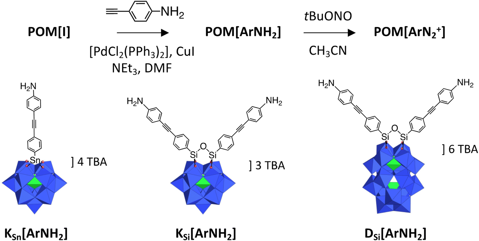 | ||
| Scheme 1 Representation of the POM hybrids KSn[ArNH2], KSi[ArNH2] and DSi[ArNH2]; WO6 and PO4 centers are depicted by blue octahedra and green tetrahedra respectively, with metal atoms and heteroatom P located at the center and oxygen atoms located at the apex of polyhedral. The synthetic route for the POM hybrids of this work is also depicted. | ||
The remote aniline groups ArNH2 enable the generation of diazonium groups ArN2+ which can be easily activated to produce corresponding aryl radicals along with N2 release. In turn, we expect those radicals to covalently bind on the electrode surface and also to react with neighboring aromatic rings to yield a cross-linked POM-based molecular film, tightly adhered to the substrate. A proposed schematic illustration of the POM molecular film is given in Scheme 2. In our previous studies, the POM hybrids with remote diazonium groups were isolated prior to their grafting on various electrodes.20,26,30–33 The multi-step synthetic pathway involves the preparation of POM hybrids with protected diazonium groups in the form of triazene derivatives and their subsequent deprotection through the addition of trifluoroacetic acid. This ensures the purity of the starting materials, albeit of short life-time, but the use of strong acid also introduces protons as possible POM counter cations. The electrochemical properties of POMs are strongly dependent on their counter cations; therefore, this protection–deprotection step was found to complicate the electrochemical features of the film after grafting.31 For sake of simplicity and to avoid the introduction of adventitious protons, we thus decided to in situ generate the diazonium groups, using a large excess of alkyl-nitrite in an organic solvent, which is largely exemplified in the literature.34 With reference to the NMR information for [PW11O39{SnC6H4-CC-C6H4N2+}]3−KSn[ArN2+] from our previous studies,20 the diazonium groups from [PW11O39{SnC6H4-CC-C6H4NH2}]4− could be readily monitored, as depicted in Fig. 1. After the addition of five equivalents of tBuONO new peaks appeared but the resulting spectrum recorded a mixture of compounds. From our experiments, it required at least fifteen equivalents of tBuONO to give rise to the set of signals characteristics of the aryl diazonium function. Further increasing the amount of tBuONO revealed no significant impact. On the other hand, for DSi[ArNH2], the addition of tBuONO only led to a broadening of the peaks. A plausible explanation is that silyl derivatives contain two remote organic functions, which increase intermolecular electrostatic interactions between the POM and the positively charged organic arms and favor their aggregation in solution, as we have observed with other systems.35 As it was difficult to follow the effect of increasing amounts of tBuONO on DSi[ArNH2], we decided to arbitrarily use 15 equivalents determined from the monitoring with KSn[ArNH2] for the subsequent grafting studies described in this work. It is also notable that the attempts to isolate the diazonium substituted POMs from NOBF4 were not successful as previously noted.26 The generation of the diazonium functions reduces the overall charge of the POM hybrids. As a result, the in situ generated KSi[ArN2+] with a single negative charge was poorly soluble in acetonitrile. We thus decided to further investigate the formation of the POM-based film mostly from DSi[ArN2+], which has an overall charge of 4−.
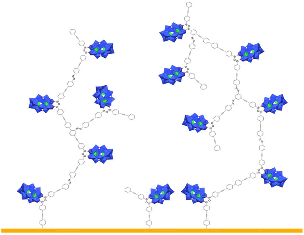 | ||
| Scheme 2 Proposed schematic illustration of the POM-based molecular film that could form on the electrode by electro-activation of the in situ generated diazonium substituted POM hybrid DSi[ArN2+]. | ||
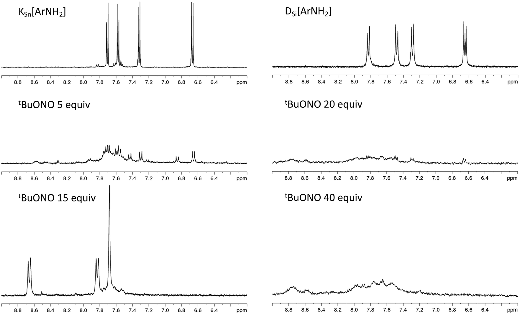 | ||
| Fig. 1 1H NMR monitoring of the formation of the diazonium substituted POM hybrids KSn[ArN2+] (left) and DSi[ArN2+] (right), from KSn[ArNH2] and DSi[ArNH2] respectively, in the presence of an increasing amount of tBuONO. | ||
Formation of a POM-based molecular film onto ITO
The grafting took place in a three-electrode electrochemical cell, comprising the ITO substrate as the working electrode, a saturated calomel electrode (SCE) as the reference electrode and a Pt counter electrode.A solution of 1 mM POM hybrid DSi[ArNH2] was prepared in 0.1 M TBAPF6 in acetonitrile. Upon the addition of 15 equivalents of tBuONO, the formation of a small amount of as yet non-identified precipitate was observed, which might correspond to some POM oligomers. As this is considered undesirable in the close vicinity of the substrate, a five-minute delay was included in our preparation protocol, allowing the precipitate to deposit at the bottom of the cell before the electro-grafting process. Reduction of the in situ formed diazonium function was achieved by applying a potentiodynamic cycle between 0 and −1 V vs. SCE, at a sweep rate of 0.3 V s−1 for 10 times.
After grafting, the ITO substrate was thoroughly washed with CH3CN and DMSO and set back in the cell containing only the supporting electrolyte. Cyclic voltammograms are then run to confirm the presence of immobilized POMs on the substrate (Fig. 2 and S8† for a DSi[Ar] film and a KSi[Ar] film, respectively). In this context, two well defined redox couples are observed, with a first cathodic peak Epc at −0.622 V per SCE and the corresponding anodic peak Epa at −0.568 V per SCE (ΔEp = Epa − Epc = 0.054 V; E1/2 = 1/2(Epa + Epc) = −0.595 V) for DSi[Ar], which agrees well with the electrochemical behavior of DSi[ArNH2] in solution (Fig. S7†) and the E1/2 = −0.57 V per SCE value previously reported for analogous organo-silyl derivatives of Dawson-type POM hybrids in CH3CN solution, at a glassy carbon electrode.36,37 Whereas a value of ΔEp = 0 is expected for immobilized species, non-ideal values of ΔEp have already been observed in our previous studies, implying a slow electron transfer rate. This has been ascribed to a charge effect due to the polyanionic character of the POMs.26,33 Consistently, a lower ΔEp = 0.019 V value is ascribed to a KSi[Ar] film, with Keggin anions of lower charge (Fig. S8†). The POM immobilization at the ITO electrode is also supported by the linear variation of the first cathodic peak intensity with the voltage sweep-rate.
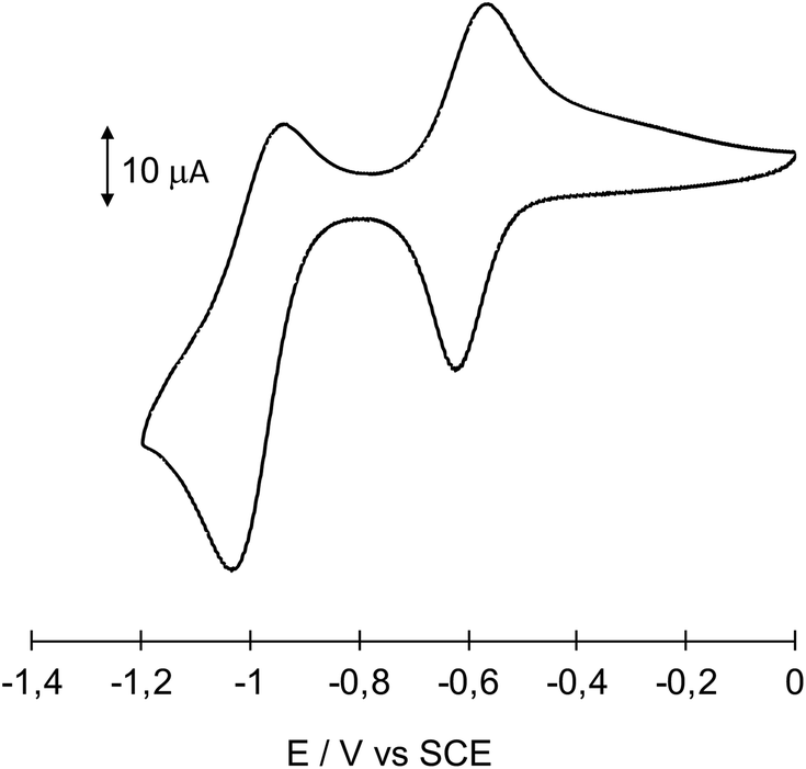 | ||
| Fig. 2 Cyclic voltammogram of immobilized DSi[Ar] in CH3CN (0.1 M TBAPF6) at an ITO electrode, potentials given versus SCE electrode, scan rate 0.3 V s−1. | ||
By using the faradaic equation, the integration of the first reduction peak has been used to assess the surface coverage of POMs Γ, with the assumption that all immobilized species are electro-active and that the electrode surface area is accurately known.19,26 In the case of a monolayer of covalently grafted [PW11O39{SnC6H4-CC-C6H4-}]4−, Γ values have been found in the range 9.2 × 10⁻¹¹ mol cm−2 (onto glassy C) to 10−10 mol cm−2 (onto Si), which is consistent with the values obtained with other molecules like porphyrins or ferrocene and corresponds to a densely packed monolayer.38 This will be used as a benchmark value in the following, as an indicator of the efficiency of the grafting. We will discuss later on the limits of this indicator. Integration of the first reduction peak in Fig. 2 gives Γ = 1.4 × 10⁻¹⁰ mol cm−2 for the DSi[Ar] film. A lower value of 1.1 × 10⁻¹¹ mol cm−2 was calculated for the KSi[Ar] film described in Fig. S8,† which could be related to the lower solubility of the diazonium precursor. The Γ values calculated for the DSi[Ar] films are higher than those of a monolayer of covalently grafted [PW11O39{SnC6H4-CC-C6H4-}]4− (KSn[Ar]) as previously reported but much lower than what we expected for a thick film. Moreover, batch-to-batch variability was observed, with values generally in the range 0.7–2.4 × 10⁻¹⁰ mol cm−2 (mean value 1.5 on about twenty grafting experiments). This prompted us to further characterize the substrates. An AFM image of a representative film is presented in Fig. 3 together with a height profile, revealing a thick holey film of several hundreds of nm (Fig. 3, left). In some other cases, the film appeared to cover the substrate but still with deep valleys (Fig. 3, middle). Further insights were given by scanning electron microscopy analysis coupled with energy-dispersive X-ray spectroscopy (SEM-EDS), run either at the top of the film or in a depleted zone, as depicted in Fig. 4. Whereas the expected peak corresponding to tungsten is observed when the spectrum is recorded in the depleted region, it is completely concealed by intense carbon, fluoride and phosphorus peaks that dominate the EDS spectrum of the top regions. This unveils that the POM layer is coated with an imperfect but thick layer of the supporting electrolyte TBAPF6, that has resisted thorough washing with CH3CN and DMSO. A similar behavior has been observed with 4-iodoaniline and cannot thus be ascribed to the POMs. Fortunately, the electrolyte coating can be eliminated by ultrasonication of the substrate in pure CH3CN for ten minutes as demonstrated by the AFM image on Fig. 3 (right) and a height profile of a few nanometers.
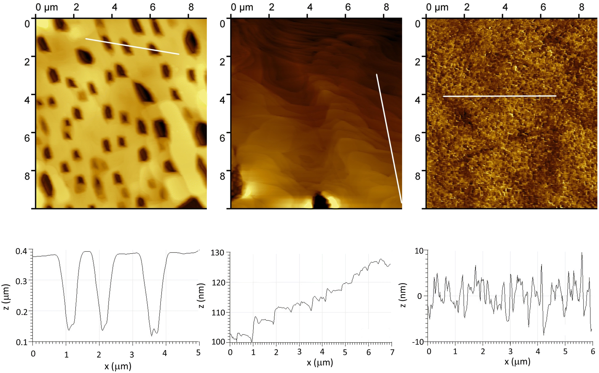 | ||
| Fig. 3 AFM images (top) and profiles (bottom) of typical thick irregular films deposited onto ITO upon electrografting of DSi[ArN2+] in the presence of TBAPF6 electrolyte after a simple rinsing with CH3CN and DMSO (left and middle) and AFM image and profile of the POM film retrieved after sonication in CH3CN. | ||
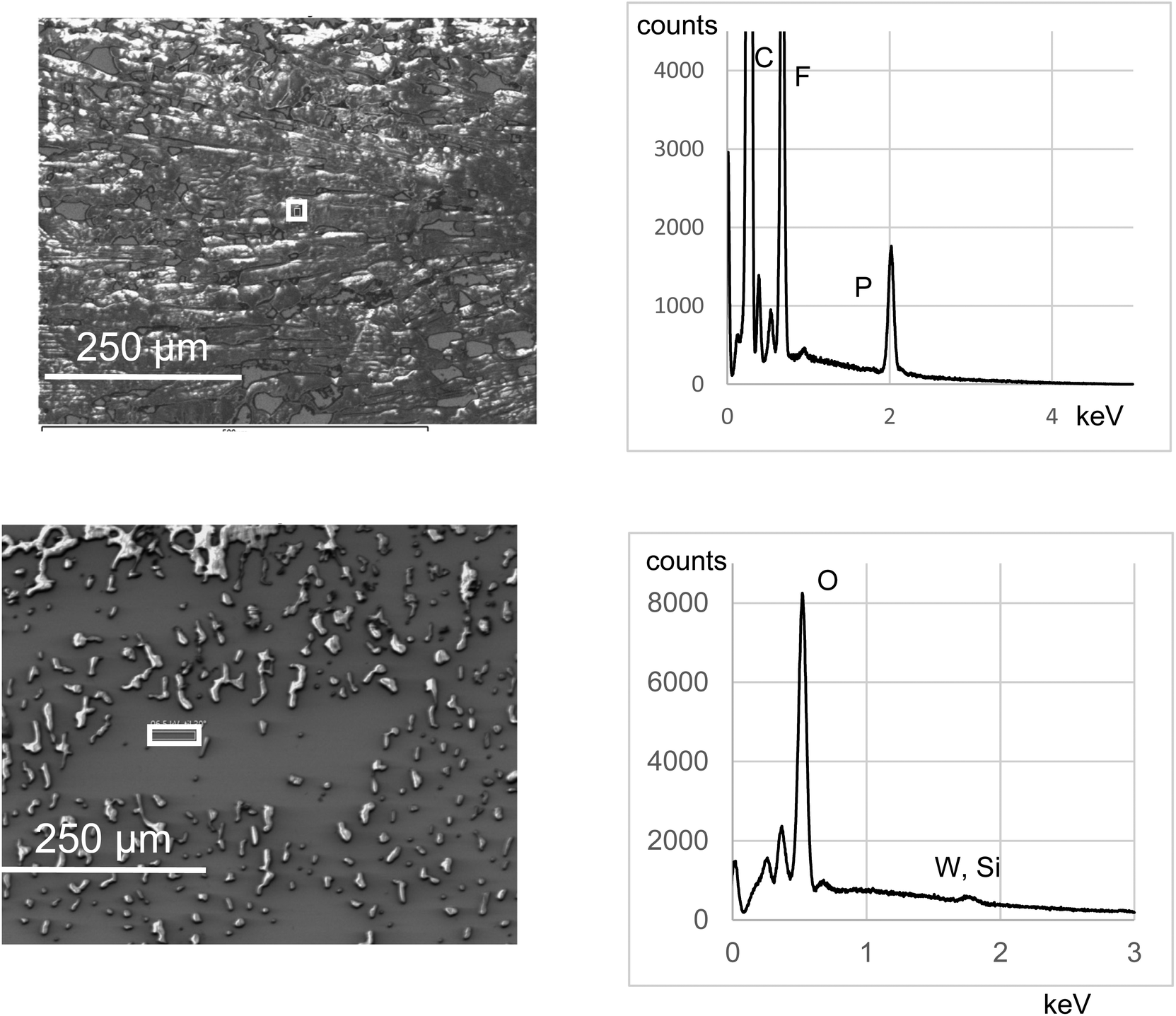 | ||
| Fig. 4 (Left) SEM images of a crude film deposited onto ITO upon electrografting of DSi[ArN2+] in the presence of TBAPF6 electrolyte with simple rinsing and no sonication and (right) EDS analysis on top of the film (top) and in a depleted zone (bottom). | ||
Adjustment of the grafting protocol – multi-graftings
The effect of several parameters on the grafting has been investigated and analyzed on the basis of the apparent Γ values, taken as a rough indicator to determine the efficiency of the grafting (see Table S1†). When the DSi[ArNH2] concentration varies from 0.2 to 2 mM, the corresponding Γ would first increase, from 0.2 to 1 mM, and then slightly decrease. With that, a POM concentration of 1 mM was thus deployed in the final protocol. The number of potential cycles (up to 65) turned out to have little effect. The choice of the potential range could have had more impact: as the film is growing, its conductivity is expected to decrease (it becomes more insulating) which in turn would impair the electron transfer from the electrode to the diazonium-terminated POMs and thus further film growth. It has been suggested in the literature that this can be mitigated by using an electroactive species as an electron mediator,39 a role that the POMs could fulfill.40 The dediazonation (reduction of the diazonium and N2 release) occurs around −0.3 V per SCE, while the first two reduction processes on the Dawson-type DSi POM hybrids have been measured at −0.57 and −0.94 V per SCE (cathodic peaks Epc). We have thus chosen three potential windows, [0; −0.5 V], [0; −0.75 V] and [0; −1 V], restricted to the reduction of the diazonium function and progressively adding the first and the second redox process of the POM. No clear-cut conclusion could be drawn and we thus kept the widest potential window [0; −1 V] for the subsequent grafting.We also tried to increase the Γ value by repeating the electrografting procedure with a renewed DSi[ArNH2] solution and an already modified ITO substrate, after washing and sonication to remove TBAPF6 electrolyte (see above): double, quadruple and sextuple graftings have thus been performed and generally correspond to an increase of Γ from double (Γ2 = 1.4 × 10⁻¹⁰ mol cm−2) to quadruple (Γ4 = 3.5 × 10⁻¹⁰ mol cm−2) and sixfold (Γ6 = 6.2 × 10⁻¹⁰ mol cm−2) grafted surfaces. Typical values of Γ2 range from 1.1 to 2.7 × 10⁻¹⁰ mol cm−2 on about twenty experiments, with a mean value of 1.7. Our results clearly differ from those obtained for molecular wires assembled by stepwise incorporation of metal centers, under either coordination driven processes41,42 or iterative electrosynthesis,43 where the current was shown to increase proportionally or even linearly with the number of steps. This might be ascribed to the lower organization of the POMs in our materials and the amorphous character of the films.
Characterization of the POM-based molecular films onto ITO
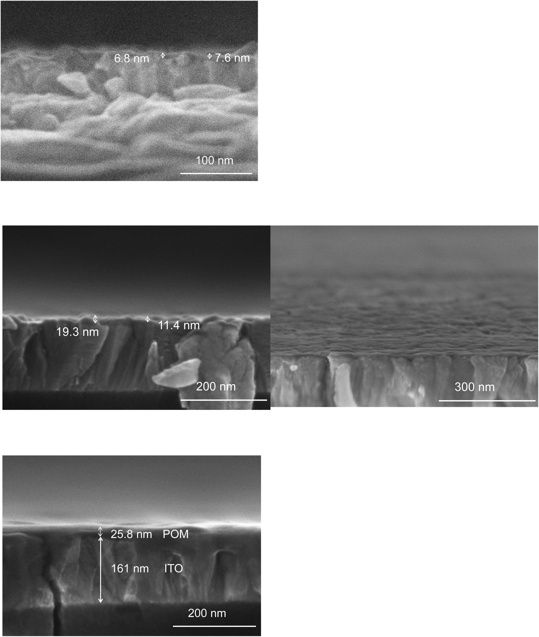 | ||
| Fig. 5 FESEM images of DSi[Ar] films electrodeposited onto ITO after mono- (top), double- (middle) and quadruple-grafting (bottom). | ||
A possible explanation for the underestimation of Γ is the low conductivity of the film, owing to the presence of bulky tetrabutylammonium cations, used both as POM charge balancing counter ions and also as electrolyte cations, likely with a low mobility inside the film. This hypothesis is substantiated by a complementary test where TBAPF6 has been replaced by LiBF4. In this experiment, LiBF4 was used as electrolyte in both the double-grafting and post-grafting analysis by cyclic-voltammetry. The Γ value extracted from the cyclic-voltammogram recorded in these conditions was compared to that extracted from the cyclic-votammogram recorded on the same modified substrate but using TBAPF6 as the electrolyte and was found to be four times higher: Γ2,Li = 3.9 × 10⁻¹⁰ mol cm−2 compared to Γ2,TBA = 1.0 × 10⁻¹⁰ mol cm−2. A film porous enough or, as proposed above, better organized to allow the penetration of the electrolyte and cations as small as possible would thus be preferable. Yet, FESEM characterization of the film give images similar to those previously displayed in Fig. 5 for double-grafted films, with no obvious increase in the thickness (see Fig. S13†).
Some of us have previously reported on the formation of monolayers of [PM11O39{XC6H4-CC-C6H4-}]4− (M = Mo, W, X = Ge, Sn) on various substrates, glassy-carbon,26,31,33 graphene,32 gold30 and silicon.19,20 In these studies, the diazonium precursors [PM11O39{XC6H4-CC-C6H4-N2+}]3− were independently prepared, prior to their redissolution and activation in solution for subsequent (electro)-chemical grafting. This differs from the present work, where the diazonium-terminated POMs have been generated in situ. The formation of a covalently bonded POM monolayer in the previous cases was supported by measurements by ellipsometry when possible (Si and Au), indicating a few nanometer thick layer (2.3 to nm) and consistent with the Γ values (9.2 × 10⁻¹¹ mol cm−2 onto glassy carbon to 10−10 mol cm−2 onto Si), which were very reproducible. It is well known that diazonium is prone to forming multi-layers24,25,39 and we propose that the stop at the monolayer stage was due to some steric hindrance brought by the POMs.26 Surprisingly, in the present case, starting from (TBA)4[PW11O39{SnC6H4-CC-C6H4NH2}] KSn[ArNH2] and generating the diazonium function in situ by the addition of an excess of tBuONO, a higher Γ value was extracted from the CV after mono-grafting onto glassy carbon, up to 1.6 × 10⁻¹⁰ mol cm−2. After mono-grafting onto ITO, the Γ values were lower than those obtained from DSi[ArNH2] (Γ = 1.9–4.1 × 10⁻¹¹ mol cm−2) but the thickness disclosed on the SEM images, about 10 nm, was definitely higher than that of a monolayer (Fig. S14†). To solve this apparent contradiction and as a control experiment, another grafting onto ITO in every respect similar to the previous one except for the use of pre-isolated (TBA)3[PW11O39{SnC6H4-CC-C6H4-N2+}] instead of KSn[ArNH2]/tBuONO was carried out. No layer was visible on the SEM image, even if the POM presence was confirmed by cyclic-voltammetry and XPS, indicating that the grafted film was thinner than 5 nm, fully consistent with our previous conclusions. This underscores the great care that should always be taken in setting up the experimental conditions. It indicates that the in situ generation of the diazonium functions is convenient but probably generates more radicals in solution due to the excess of tBuONO and then a loss of control of the grafting process. Yet, it allows for the formation of the targeted thick (in the sense thicker than a monolayer) films.
![[double bond, length as m-dash]](https://www.rsc.org/images/entities/char_e001.gif) N–) resulting from the reaction between a diazenyl radical and an outer aromatic ring (or an aryl radical and a diazonium group), so bridging two POM hybrids.44 There is no peak around 403.8 eV that would point to the presence of some diazonium groups.45 This drove us to propose the schematic illustration of the POM-based molecular film in Scheme 2.
N–) resulting from the reaction between a diazenyl radical and an outer aromatic ring (or an aryl radical and a diazonium group), so bridging two POM hybrids.44 There is no peak around 403.8 eV that would point to the presence of some diazonium groups.45 This drove us to propose the schematic illustration of the POM-based molecular film in Scheme 2.
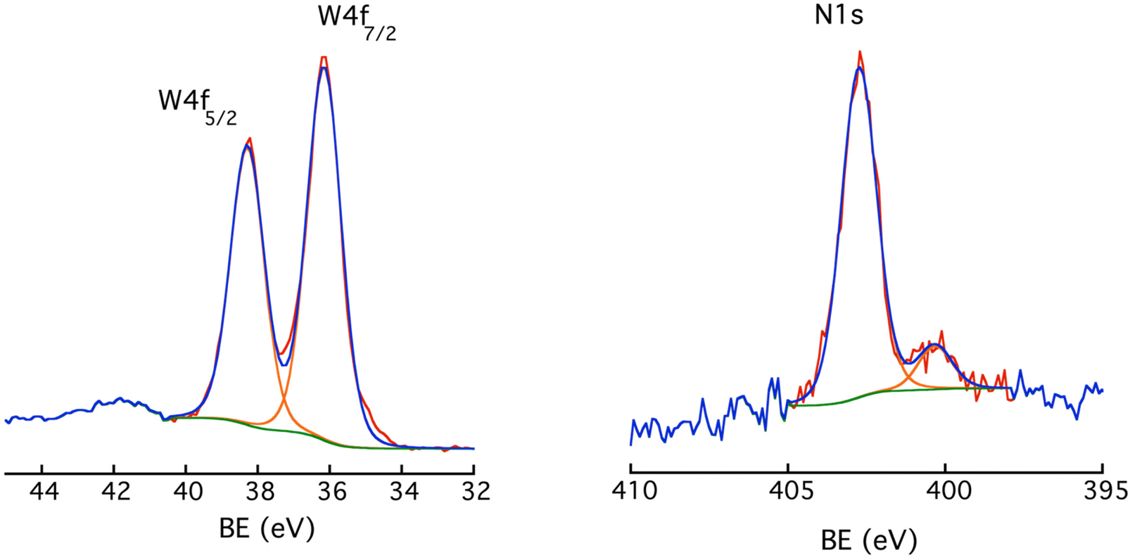 | ||
| Fig. 6 High resolution X-ray photoelectron spectra for (left) W 4f and (right) N 1s for a DSi[Ar] film electrodeposited onto ITO (double grafting). | ||
Memory tests
Organic and hybrid resistive switching materials and devices attract special attention because of the tunability of their properties by molecular design and their mechanical flexibility suitable for wearable applications.46 To gain insights into the resistive switching characteristics of a DSi[Ar]-modified ITO substrate, prepared as previously described and characterized, gold electrodes are thermally evaporated through a shadow mask and deposited on the POM films (double grafting), forming electrodes with an area of 0.25 mm2. The current–voltage (I–V) curves are recorded by applying a bias between the gold top electrode and the bottom ITO electrode, resulting in a two-terminal memory device configuration. At 0 V, the device is in the OFF state (high resistance/low conductance). When a negative bias is applied, the current increases gradually and then abruptly rises at a voltage of about −1 V to −1.5 V to reach the ON state (low resistance/high conductance), known as the SET voltage (Fig. 7, left). This transition process can be regarded as the writing process for a bistable memory device. Further investigation reveals that this memory could be preserved in the subsequent sweep from 0 to +2 V as well as from 0 to −2 V. The device remains in the ON state even upon removal of the electric field, suggesting that the device is exhibiting nonvolatile memory behavior. Further application of reversed bias up to 5 V could not return the device to its original state. Such a memory characteristic can be envisioned as a consequence of charge-trapping within the POM, leading a permanent change in film conductivity. Note however that in about 5% of our tests reversible, rewritable memory behavior (also referred to as flash) was observed. The reason is still not clear but could be related to a lower thickness of the POM film (Fig. S16†), resulting in a reversible charge/discharge within the film.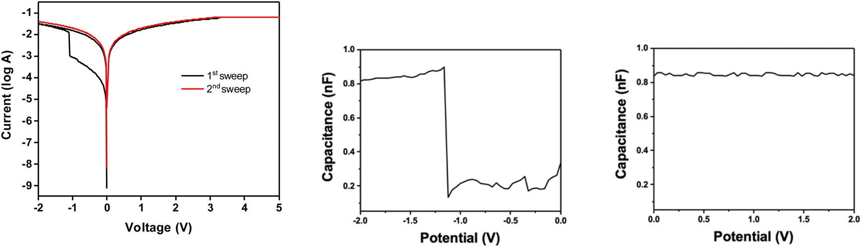 | ||
| Fig. 7 Left: I–V characteristics of a DSi[Ar] film in a device configuration: first sweep from 0 to −2 V and sweep back to 0 and +2 V; capacitance measurements showing the OFF to ON state transition (middle) and the stability of the ON state upon reversal of the potential (right). | ||
The SET voltages variations on a given substrate and their variations from one substrate to another are quite important (Fig. S17†). The batch-to-batch performance of devices from the same substrate shows a narrow SET voltage distribution, but the SET voltages of a different substrate could come out quite different, even following the same grafting conditions and the same POM batch. For example, out of the 20 devices on one substrate, 8 devices were successfully turned ON with an average SET potential of 1.105 ± 0.069 V, while for another substrate, 9 devices showed an average SET potential of 1.612 ± 0.163 V. This can probably be ascribed to the poor molecular organization of the POMs inside the film upon the electro-grafting process.
It has also been shown that by applying a constant reading voltage at 0.5 V, there was no significant degradation in the current value of the ON-state device over 104 s (Fig. S18†), indicating that the POM film is electrically robust with a low misreading rate.
The charge trapping attribute has been validated by capacitance–voltage measurements from 0 to −2 V at 0.5 MHz (Fig. 7, middle and right). In brief, the capacitance displayed a steep jump at about −1.2 V to reach a 0.84 nF value that would roughly correspond to a reduction of less than 1 over 10![[thin space (1/6-em)]](https://www.rsc.org/images/entities/char_2009.gif) 000 electroactive POMs as estimated from the first electrochemical reduction process (the integration of the first reduction wave corresponds to a charge of 1.26 × 10⁻⁵ C, for a substate of 1 cm2 and thus a Γ = 1.3 × 10⁻¹⁰ mol cm−2 value, to be compared to a charge of about 10−9 C for a capacitance value of 0.84 nF at −1.2 V). It is lower than the few percent measured on monolayers of other redox active molecules like ferrocene47 or in organic transistor memories48 (data that are actually rarely given), and tentatively ascribed to the low mobility of the tetrabutylammonium counter ions. It is noteworthy that a detrimental effect of large cations has been reported in POM-based electrochromic materials,49 where the blue color change associated with the reduction of the POMs cannot be observed in the absence of small cations such as lithium or protons,50 sometimes leading to the addition of lithium perchlorate electrolyte in the fabrication process.51 The low mobility of the tetrabutylammonium counter ions could also account for the WORM type behavior/irreversibility. Indeed, the role of the counter ions in the width of the hysteresis loop has been pointed out.52 More generally, the nature of the switching mechanism in molecular junctions based on redox-active molecules is still a wide open question, the stabilization of the injected charges through counterion migration being less easy in the solid state than in solution.53
000 electroactive POMs as estimated from the first electrochemical reduction process (the integration of the first reduction wave corresponds to a charge of 1.26 × 10⁻⁵ C, for a substate of 1 cm2 and thus a Γ = 1.3 × 10⁻¹⁰ mol cm−2 value, to be compared to a charge of about 10−9 C for a capacitance value of 0.84 nF at −1.2 V). It is lower than the few percent measured on monolayers of other redox active molecules like ferrocene47 or in organic transistor memories48 (data that are actually rarely given), and tentatively ascribed to the low mobility of the tetrabutylammonium counter ions. It is noteworthy that a detrimental effect of large cations has been reported in POM-based electrochromic materials,49 where the blue color change associated with the reduction of the POMs cannot be observed in the absence of small cations such as lithium or protons,50 sometimes leading to the addition of lithium perchlorate electrolyte in the fabrication process.51 The low mobility of the tetrabutylammonium counter ions could also account for the WORM type behavior/irreversibility. Indeed, the role of the counter ions in the width of the hysteresis loop has been pointed out.52 More generally, the nature of the switching mechanism in molecular junctions based on redox-active molecules is still a wide open question, the stabilization of the injected charges through counterion migration being less easy in the solid state than in solution.53
Conclusions
The ultimate properties of POM-based materials are impacted by their shaping process. We have drawn on our expertise of POM hybrids to devise bis-silyl and mono-tin derivatives of Keggin- and Dawson-type polyoxotungstates featuring remote arylamine groups. As anticipated, in situ generated diazonium functions are prone to forming covalent films a few nanometers thick on the ITO electrode, that have been characterized by electrochemistry and microscopies (AFM and FESEM), together with XPS. We thus provide a path to extended covalent networks of cross-linked POMs, which are still rare,15,54 at an intermediate scale between monolayers and several hundred nanometers thick films. The resistive switching of the as-prepared films has been disclosed and a WORM-type behavior observed, with a low set voltage. The memory is not rewritable. Yet, it is also precedented that in a given family of molecules manipulation of the electronic structure or material elaboration can change the electrical behavior from a WORM- to a flash-type memory.55–57 There is thus plenty of room to play with the molecular diversity of POMs and the tunability of their redox properties to tune the set voltages at which the device switches from the OFF to the ON state and to facilitate charge de-trapping upon application of a reverse bias.Both the electrochemical study in the solution phase and the electrical characterization in the solid-state pinpoint a unique feature of polyoxometalates: they are polyanions, with counter-cations that do much more than static balancing of the overall charge.58,59 The shaping process we have chosen involves organic–inorganic POM hybrids that have to be prepared in organic solvents. For solubility reasons, the counter-cations commonly used are thus bulky tetraalkylammonium. Beyond the effect on the structure of the materials, this slows down their migration upon electron transfers to and from the POMs. It is only very recently that the effect of the mobility of ions on the electrical characteristics of molecular tunnel junctions has been addressed.60 Up to now molecular electronics has rather considered redox active molecules neutral. Polyoxometalate chemistry thus provides a unique opportunity to further involve ionic species61 and to harness the influence of counterions to explore possibly emerging properties.
Experimental section
General
Chemicals and solvents were used as supplied. (TBA)4[PW11O39{SnC6H4I}] KSn[I], (TBA)3[PW11O39{(SiC6H4I)2O}] KSi[I] and (TBA)6[P2W17O61{(SiC6H4I)2O}] DSi[I] were prepared as previously reported by some of us.27,281H and 31P NMR spectra were recorded on Bruker Avance III 300 MHz and 400 MHz spectrometers, equipped with BBFO probes. 1H spectra are referenced according to tetramethylsilane, with solvent signals used as internal references. 31P spectra are referenced according to phosphoric acid at 85%. The IR spectrum of the powder was recorded from a KBr pellet on a Jasco FT/IR 4100 spectrometer. Elemental analyses were performed at the Faculty of Pharmacy in Orsay. High-resolution ESI mass spectra were recorded on a Q-Tof instrument (timsTOF™) equipped with an electrospray ionization (ESI) source in negative ion mode. Samples (10−5 mol L−1 solution in CH3CN) were injected at a flow rate of 3 μl min−1. The instrumental parameters were set as follows: electrospray voltage of 3500 V, end plate offset at 500 V, and capillary temperature at 200 °C. As the nebulizer and drying gas, the nitrogen flow was fixed at 0.3 bar and 3 L min−1, respectively. Mass spectra were recorded in a range of 150–2500 m/z with a transfer time of 110 μs and a pre-pulse storage of 10 μs. Therefore, external calibrations in m/z (in quadratic mode) were carried out using the ESI-L low concentration tuning mix solution. Cyclic voltammetry experiments were carried out on an Autolab PGSTAT 100 from Metrohm, using a classical three-electrode cell, with a working electrode (glassy C or ITO substrate), a Pt counter electrode and a saturated Hg2Cl2/KCl reference electrode (SCE) fitted with a bridge containing a saturated aqueous LiCl solution. For the sake of comparison with other systems, the oxidation potential of ferrocene recorded in such conditions in CH3CN is 0.424 V.ITO substrates (glass +150 nm ITO, average roughness 3 nm) were purchased from Kintec company (Hong-Kong). The substrates were cleaned by two successive ultrasonicate baths in acetone and ethanol. The surface morphology of the POM films was determined by imaging with a Nanoscope VIII multimode atomic force microscope (AFM) from Bruker equipped with a 150 × 150 × 5 μm scanner. Silicon cantilevers (from Brucker; k = 0.4 N m−1, radius ∼10 nm) were used to acquire AFM images in peak force tapping mode in air at room temperature (1 × 1 μm2 at 1 Hz with a resolution of 512 × 512 pixels). c-AFM measurements were carried out on a Nano-Observer from Scientec. Electrical measurements were acquired through a “resiscope”, a set-up developed by the Génie Electrique et Electronique de Paris to perform SSRM-like measurements over a dynamic range of 1010 Ω. Two types of conductive tips with a Pt/Ir coating both sides were used: 240 AC-PP from μmasch with a stiffness given at 2 N m−1 (v = 70 kHz) and PPP-NCLPt from Nanosensors (for fine measurements), with a stiffness given at 48 N m−1 (v = 190 kHz). In both cases, the tip radius was 20 nm, and the height was 15 μm. Field emission scanning electron microscopy (FESEM) was carried out on a Hitachi SU-70 microscope, with an Oxford X-Max 50 mm 2 detector for energy dispersive X-ray spectroscopy (EDS), at the Institut des Matériaux de Paris Centre. Images and EDS analysis were obtained with an electron beam at a voltage of 5 kV. X-Ray photoelectron spectroscopy (XPS) was performed on an Omicron Argus X-ray photoelectron spectrometer. The monochromated AlKα radiation source (hν = 1486.6 eV) had a 280 W electron beam power. The emission of photoelectrons from the sample was analyzed at a takeoff angle of 45° under ultra-high vacuum conditions (≤10−9 mBar). Spectra were carried out with a 100 eV pass energy for the survey scan and 20 eV pass energy for the core level regions. Binding energies were calibrated against the C 1s (C–C) binding energy at 284.8 eV and element peak intensities were corrected by Scofield factors. The spectra were fitted using Casa XPS v.2.3.15 software (Casa Software Ltd, U.K.) and applying a Gaussian/Lorentzian ratio G/L equal to 70/30.
Memory devices were fabricated by thermally evaporating 100 nm thick gold top electrodes onto the POM film through a shadow mask. The resulting devices had an approximate area of 0.25 mm2. The current–voltage (I–V) characteristics of these memory devices were evaluated under ambient conditions in a probe station equipped with the Keysight B1500A semiconductor device parameter analyzer. The capacitances of the devices were also measured by the Keysight (Agilent) LCR meter.
![[triple bond, length as m-dash]](https://www.rsc.org/images/entities/b_char_e002.gif) C-C6H4NH2}] (KSn[ArNH2]).
KSn[I] (390 mg, 0.098 mmol), 4-ethynylaniline (30.9 mg, 0.264 mmol, 2.69 equiv.), [PdCl2(PPh3)2] (11.8 mg, 0.017 mmol, 0.17 equiv.) and CuI (3.9 mg, 0.020 mmol, 0.20 equiv.) are added to a dried Schlenk flask under an Ar atmosphere with 5 mL of dried DMF and distilled TEA (270 μL, 1.96 mmol, 20 equiv.). The solution is stirred overnight at ambient temperature and precipitated in ether. After centrifugation, the obtained solid is dissolved in a minimum of acetonitrile with TBABr (300 mg, 0.931 mmol, 9.5 equiv.). The solution is precipitated in ethanol and centrifugated and the slightly brown solid is washed in ethanol and in ether (yield 61%, 236.5 mg). 1H NMR (400 MHz, CD3CN): δ (ppm) 7.68 (d + dd, JH–H = 8.2 Hz, JSn–H = 95.4 Hz, 2H), 7.55 (d + dd, JH–H = 8.2 Hz, JSn–H = 34.2 Hz, 2H), 7.29 (d, JH–H = 8.7 Hz, 2H), 6.64 (d, J = 8.7 Hz, 2H), 4.46 (s, 2H), 3.12 (m, 32H), 1.63 (m, 32H, N-CH2-CH2-CH2-CH3), δ = 1.39 (sex, J = 7.4 Hz, 32H), 0.98 (t, J = 7.4 Hz, 48H). 31P NMR (162 MHz, CD3CN): δ (ppm) −10.98 (s + d, JSn–P = 23.1 Hz). IR (KBr, cm−1): 2960 (m), 2933 (m), 2873 (m), 1483 (m), 1380 (f), 1069 (F), 962 (F), 886 (F), 813 (FF), 515 (f), 380 (m). Anal. Calcd for PW11O39SnC78H154N5 (%): C, 23.67; H, 3.92; N, 1.78 Found: C, 23.52; H, 3.80; N, 1.66. HRMS (ESI−): m/z: 747.06 [M]4− calcd 747.06; 996.41 [M + H]3− calcd 996.41; 1076.84 [M + TBA]3− calcd 1076.84; 1615.76 [M + 2TBA]2− calcd 1615.76.
C-C6H4NH2)2O}] KSi[ArNH2].
KSi[I] (100 mg, 0.026 mmol), 4-ethynylaniline (19 mg, 0.16 mmol, 6 equiv.) [PdCl2(PPh3)2] (2.3 mg, 0.0033 mmol, 0.1 equiv.) and CuI (1 mg, 0.053 mmol, 0.2equiv.) were added to a dried Schlenk flask under an Ar atmosphere with 2 mL of dried DMF and distilled TEA (100 μL, 0.70 mmol, 27 equiv.). The solution was stirred overnight at ambient temperature and precipitated in diethyl ether. After centrifugation, the obtained solid was dissolved in a minimum of acetonitrile with TBABr (100 mg, 0.31 mmol, 11.9 equiv.). The solution was precipitated with absolute ethanol and centrifuged, and the recovered solid was washed with ethanol and ether. 1H NMR (300 MHz, CD3CN): δ (ppm) 7.82 (d, J = 8.1 Hz, 4H), 7.55 (d, J = 8.1 Hz, 4H), 7.29 (d, J = 8.6 Hz, 4H), 6.64 (d, J = 8.6 Hz, 4H), 4.47 (s, 4H), 3.09 (m, 24H), 1.61 (m, 24H), 1.37 (sex, J = 7.3 Hz, 24H), 0.97 (t, J = 7.3 Hz, 36H). 31P NMR (121.5 MHz, CD3CN, ppm): δ (ppm) −12.83 (s, 1P). IR (KBr, cm−1): 3457 (s), 3384 (s), 2961 (s), 2933 (m), 2874 (m), 2206 (w), 1624 (s), 1594 (s), 1519 (s), 1480 (m), 1383 (w), 1109 (s), 1066 (m), 1038 (s), 965 (vs), 873 (vs), 823 (vs), 767 (m), 712 (m), 590 (m), 523 (m). Anal. Cald (%): C, 23.64; H, 3.34; N, 1.81 Found: C, 23.64; H, 3.07; N, 1.70. HRMS (ESI−): m/z: 1044.45 [M]3− calcd 1044.45; 1688.81 [M + TBA]2− calcd 1688.82.
C-C6H4NH2)2O}] DSi[ArNH2].
DSi[I] (100 mg, 0.016 mmol), 4-ethynylaniline (10 mg, 0.085 mmol, 5 eq.) [PdCl2(PPh3)2] (1.1 mg, 0.0016 mmol, 0.10 eq.) and CuI (0.5 mg, 0.0026 mmol, 0.15 eq.) were added to a dried Schlenk flask under an Ar atmosphere with 2 mL anhydrous DMF and distilled TEA (100 μL, 0.70 mmol, 44 eq.). The solution was stirred overnight at ambient temperature and precipitated in diethyl ether. After centrifugation, the solid obtained was dissolved in minimum acetonitrile with TBABr (100 mg, 0.31 mmol, 19.4 eq.). The solution was precipitated with absolute ethanol and centrifuged, and the recovered solid was washed with ethanol and ether (yield 76.2%, 76 mg). 1H NMR (300 MHz, CD3CN): δ (ppm) 7.82 (d, J = 8.1 Hz, 4H), 7.47 (d, J = 8.1 Hz, 4H), 7.28 (d, J = 8.6 Hz, 4H), 6.63 (d, J = 8.6 Hz, 4H), 4.44 (s, 4H), 3.14 (m, 48H), 1.63 (m, 48H), 1.40 (sex, J = 7.3 Hz, 48H), 0.98 (t, J = 7.3 Hz, 72H). 31P NMR (121.5 MHz, CD3CN): δ (ppm) −10.13 (s, 1P), −13.14 (s, 1P). IR (KBr, cm−1): 3463 (s), 3364 (s), 3224 (m), 2962 (s), 2934 (s), 2873 (s), 2205 (w), 1626 (s), 1593 (m), 1519 (m), 1484 (s), 1380 (w), 1089 (vs), 1039 (s), 955 (vs), 915 (vs), 810 (vs), 766 (s), 602 (m), 528 (m). Anal. Cald (%) for 6 TBA+: C, 24.52; H, 3.92; N, 1.84. Anal. Cald (%) for 5.75 TBA+ and 0.25 H+: C, 23.96; H, 3.81; N, 1.80 Found C, 23.94; H, 3.51; N, 1.69. HRMS (ESI−): m/z: 924.18 [M + H]5− calcd 924.19; 972.43 [M + TBA]5− calcd 972.44; 1276.11 [M + 2TBA]4− calcd 1276.12; 1539.62 [M + 3H]3− calcd 1539.65; 1782.58 [M + 3TBA]3− calcd 1782.59.
C-C6H4NH2}] (KSn[ArNH2]).
KSn[I] (390 mg, 0.098 mmol), 4-ethynylaniline (30.9 mg, 0.264 mmol, 2.69 equiv.), [PdCl2(PPh3)2] (11.8 mg, 0.017 mmol, 0.17 equiv.) and CuI (3.9 mg, 0.020 mmol, 0.20 equiv.) are added to a dried Schlenk flask under an Ar atmosphere with 5 mL of dried DMF and distilled TEA (270 μL, 1.96 mmol, 20 equiv.). The solution is stirred overnight at ambient temperature and precipitated in ether. After centrifugation, the obtained solid is dissolved in a minimum of acetonitrile with TBABr (300 mg, 0.931 mmol, 9.5 equiv.). The solution is precipitated in ethanol and centrifugated and the slightly brown solid is washed in ethanol and in ether (yield 61%, 236.5 mg). 1H NMR (400 MHz, CD3CN): δ (ppm) 7.68 (d + dd, JH–H = 8.2 Hz, JSn–H = 95.4 Hz, 2H), 7.55 (d + dd, JH–H = 8.2 Hz, JSn–H = 34.2 Hz, 2H), 7.29 (d, JH–H = 8.7 Hz, 2H), 6.64 (d, J = 8.7 Hz, 2H), 4.46 (s, 2H), 3.12 (m, 32H), 1.63 (m, 32H, N-CH2-CH2-CH2-CH3), δ = 1.39 (sex, J = 7.4 Hz, 32H), 0.98 (t, J = 7.4 Hz, 48H). 31P NMR (162 MHz, CD3CN): δ (ppm) −10.98 (s + d, JSn–P = 23.1 Hz). IR (KBr, cm−1): 2960 (m), 2933 (m), 2873 (m), 1483 (m), 1380 (f), 1069 (F), 962 (F), 886 (F), 813 (FF), 515 (f), 380 (m). Anal. Calcd for PW11O39SnC78H154N5 (%): C, 23.67; H, 3.92; N, 1.78 Found: C, 23.52; H, 3.80; N, 1.66. HRMS (ESI−): m/z: 747.06 [M]4− calcd 747.06; 996.41 [M + H]3− calcd 996.41; 1076.84 [M + TBA]3− calcd 1076.84; 1615.76 [M + 2TBA]2− calcd 1615.76.
C-C6H4NH2)2O}] KSi[ArNH2].
KSi[I] (100 mg, 0.026 mmol), 4-ethynylaniline (19 mg, 0.16 mmol, 6 equiv.) [PdCl2(PPh3)2] (2.3 mg, 0.0033 mmol, 0.1 equiv.) and CuI (1 mg, 0.053 mmol, 0.2equiv.) were added to a dried Schlenk flask under an Ar atmosphere with 2 mL of dried DMF and distilled TEA (100 μL, 0.70 mmol, 27 equiv.). The solution was stirred overnight at ambient temperature and precipitated in diethyl ether. After centrifugation, the obtained solid was dissolved in a minimum of acetonitrile with TBABr (100 mg, 0.31 mmol, 11.9 equiv.). The solution was precipitated with absolute ethanol and centrifuged, and the recovered solid was washed with ethanol and ether. 1H NMR (300 MHz, CD3CN): δ (ppm) 7.82 (d, J = 8.1 Hz, 4H), 7.55 (d, J = 8.1 Hz, 4H), 7.29 (d, J = 8.6 Hz, 4H), 6.64 (d, J = 8.6 Hz, 4H), 4.47 (s, 4H), 3.09 (m, 24H), 1.61 (m, 24H), 1.37 (sex, J = 7.3 Hz, 24H), 0.97 (t, J = 7.3 Hz, 36H). 31P NMR (121.5 MHz, CD3CN, ppm): δ (ppm) −12.83 (s, 1P). IR (KBr, cm−1): 3457 (s), 3384 (s), 2961 (s), 2933 (m), 2874 (m), 2206 (w), 1624 (s), 1594 (s), 1519 (s), 1480 (m), 1383 (w), 1109 (s), 1066 (m), 1038 (s), 965 (vs), 873 (vs), 823 (vs), 767 (m), 712 (m), 590 (m), 523 (m). Anal. Cald (%): C, 23.64; H, 3.34; N, 1.81 Found: C, 23.64; H, 3.07; N, 1.70. HRMS (ESI−): m/z: 1044.45 [M]3− calcd 1044.45; 1688.81 [M + TBA]2− calcd 1688.82.
C-C6H4NH2)2O}] DSi[ArNH2].
DSi[I] (100 mg, 0.016 mmol), 4-ethynylaniline (10 mg, 0.085 mmol, 5 eq.) [PdCl2(PPh3)2] (1.1 mg, 0.0016 mmol, 0.10 eq.) and CuI (0.5 mg, 0.0026 mmol, 0.15 eq.) were added to a dried Schlenk flask under an Ar atmosphere with 2 mL anhydrous DMF and distilled TEA (100 μL, 0.70 mmol, 44 eq.). The solution was stirred overnight at ambient temperature and precipitated in diethyl ether. After centrifugation, the solid obtained was dissolved in minimum acetonitrile with TBABr (100 mg, 0.31 mmol, 19.4 eq.). The solution was precipitated with absolute ethanol and centrifuged, and the recovered solid was washed with ethanol and ether (yield 76.2%, 76 mg). 1H NMR (300 MHz, CD3CN): δ (ppm) 7.82 (d, J = 8.1 Hz, 4H), 7.47 (d, J = 8.1 Hz, 4H), 7.28 (d, J = 8.6 Hz, 4H), 6.63 (d, J = 8.6 Hz, 4H), 4.44 (s, 4H), 3.14 (m, 48H), 1.63 (m, 48H), 1.40 (sex, J = 7.3 Hz, 48H), 0.98 (t, J = 7.3 Hz, 72H). 31P NMR (121.5 MHz, CD3CN): δ (ppm) −10.13 (s, 1P), −13.14 (s, 1P). IR (KBr, cm−1): 3463 (s), 3364 (s), 3224 (m), 2962 (s), 2934 (s), 2873 (s), 2205 (w), 1626 (s), 1593 (m), 1519 (m), 1484 (s), 1380 (w), 1089 (vs), 1039 (s), 955 (vs), 915 (vs), 810 (vs), 766 (s), 602 (m), 528 (m). Anal. Cald (%) for 6 TBA+: C, 24.52; H, 3.92; N, 1.84. Anal. Cald (%) for 5.75 TBA+ and 0.25 H+: C, 23.96; H, 3.81; N, 1.80 Found C, 23.94; H, 3.51; N, 1.69. HRMS (ESI−): m/z: 924.18 [M + H]5− calcd 924.19; 972.43 [M + TBA]5− calcd 972.44; 1276.11 [M + 2TBA]4− calcd 1276.12; 1539.62 [M + 3H]3− calcd 1539.65; 1782.58 [M + 3TBA]3− calcd 1782.59.
Author contributions
ML and RS synthesized the POMs, the protocol was checked by CC and SA recorded the mass spectra; RS elaborated the POM the molecular films whose electrical properties were studied by WCP and LT. AM characterized the films by XPS. AP, PSL, GI and FV conceived and supervised the project. The manuscript was written by AP and PSL with the contribution of all authors, who have given approval to the final version of the manuscript.Conflicts of interest
There are no conflict of interest to declare.Acknowledgements
This work was supported by Sorbonne Université and by the CNRS. W. C. Poh was supported by the scholarship awarded by Nanyang Technological University, Singapore. RS thanks the SU-NTU joint doctoral program for his doctoral fellowship. We thank FCMat for the FESEM and EDS measurements.References
- M. Vasilopoulou, A. M. Douvas, L. C. Palilis, S. Kennou and P. Argitis, Old metal oxide clusters in new applications: Spontaneous reduction of Keggin and Dawson polyoxometalate layers by a metallic electrode for improving efficiency in organic optoelectronics, J. Am. Chem. Soc., 2015, 137(21), 6844–6856, DOI:10.1021/jacs.5b01889.
- L. Chen, W.-L. Chen, X.-L. Wang, Y.-G. Li, Z.-M. Su and E.-B. Wang, Polyoxometalates in dye-sensitized solar cells, Chem. Soc. Rev., 2019, 48(1), 260–284, 10.1039/C8CS00559A.
- L. Yang, J. Lei, J. Fan, R. Yuan, M. Zheng, J. Chen and Q. Dong, The intrinsic charge carrier behaviors and applications of polyoxometalate clusters based materials, Adv. Mater., 2021, 33(50), 2005019, DOI:10.1002/adma.202005019.
- M. Moors, J. Warneke, X. López, C. de Graaf, B. Abel and K. Y. Monakhov, Insights from adsorption and electron modification studies of polyoxometalates on surfaces for molecular memory applications, Acc. Chem. Res., 2021, 54(17), 3377–3389, DOI:10.1021/acs.accounts.1c00311.
- A. M. Douvas, E. Makarona, N. Glezos, P. Argitis, J. A. Mielczarski and E. Mielczarski, Polyoxometalate-based layered structures for charge transport control in molecular devices, ACS Nano, 2008, 2(4), 733–742, DOI:10.1021/nn700333j.
- A. Balliou, A. M. Douvas, P. Normand, D. Tsikritzis, S. Kennou, P. Argitis and N. Glezos, Tungsten polyoxometalate molecules as active nodes for dynamic carrier exchange in hybrid molecular/semiconductor capacitors, J. Appl. Phys., 2014, 116(14), 143703, DOI:10.1063/1.4897397.
- C. Busche, L. Vilà-Nadal, J. Yan, H. N. Miras, D.-L. Long, V. P. Georgiev, A. Asenov, R. H. Pedersen, N. Gadegaard, M. M. Mirza, D. J. Paul, J. M. Poblet and L. Cronin, Design and fabrication of memory devices based on nanoscale polyoxometalate clusters, Nature, 2014, 515(7528), 545–549, DOI:10.1038/nature13951.
- X. Chen, J. Pan, J. Fu, X. Zhu, C. Zhang, L. Zhou, Y. Wang, Z. Lv, Y. Zhou and S. Han, Polyoxometalates-modulated reduced graphene oxide flash memory with ambipolar trapping as bidirectional artificial synapse, Adv. Electron. Mater., 2018, 4(12), 1800444, DOI:10.1002/aelm.201800444.
- H. Tanaka, M. Akai-Kasaya, A. TermehYousefi, L. Hong, L. Fu, H. Tamukoh, D. Tanaka, T. Asai and T. Ogawa, A molecular neuromorphic network device consisting of single-walled carbon nanotubes complexed with polyoxometalate, Nat. Commun., 2018, 9(1), 2693, DOI:10.1038/s41467-018-04886-2.
- D. Banerjee, T. Kotooka, S. Azhari, Y. Usami, T. Ogawa, J. K. Gimzewski, H. Tamukoh and H. Tanaka, Emergence of in-materio intelligence from an incidental structure of a single-walled carbon nanotube–porphyrin polyoxometalate random network, Adv. Intell. Syst., 2022, 4(4), 2100145, DOI:10.1002/aisy.202100145.
- N. S. Sterin, N. Basu, M. Cahay, M. N. Satyanarayan, S. S. Mal and P. P. Das, Redox-active vanadium-based polyoxometalate as an active element in resistive switching based nonvolatile molecular memory, Phys. Status Solidi A, 2020, 217(18), 2000306, DOI:10.1002/pssa.202000306.
- M. A. Zidan, J. P. Strachan and W. D. Lu, The future of electronics based on memristive systems, Nat. Electron., 2018, 1(1), 22–29, DOI:10.1038/s41928-017-0006-8.
- Z. Wang, H. Wu, G. W. Burr, C. S. Hwang, K. L. Wang, Q. Xia and J. J. Yang, Resistive switching materials for information processing, Nat. Rev. Mater., 2020, 5(3), 173–195, DOI:10.1038/s41578-019-0159-3.
- A. S. Cherevan, S. P. Nandan, I. Roger, R. Liu, C. Streb and D. Eder, Polyoxometalates on functional substrates: Concepts, synergies, and future perspectives, Adv. Sci., 2020, 7(8), 1903511, DOI:10.1002/advs.201903511.
- B. Hu, C. Wang, J. Wang, J. Gao, K. Wang, J. Wu, G. Zhang, W. Cheng, B. Venkateswarlu, M. Wang, P. S. Lee and Q. Zhang, Inorganic–organic hybrid polymer with multiple redox for high-density data storage, Chem. Sci., 2014, 5(9), 3404–3408, 10.1039/C4SC00823E.
- X. Chen, P. Huang, X. Zhu, S. Zhuang, H. Zhu, J. Fu, A. S. Nissimagoudar, W. Li, X. Zhang, L. Zhou, Y. Wang, Z. Lv, Y. Zhou and S.-T. Han, Keggin-type polyoxometalate cluster as an active component for redox-based nonvolatile memory, Nanoscale Horiz., 2019, 4(3), 697–704, 10.1039/C8NH00366A.
- B. Chen, Y.-R. Huang, K.-Y. Song, X.-L. Lin, H.-H. Li and Z.-R. Chen, Molecular nonvolatile memory based on [α-GeW12O40]4−/metalloviologen hybrids can work at high temperature monitored by chromism, Chem. Mater., 2021, 33(6), 2178–2186, DOI:10.1021/acs.chemmater.1c00090.
- A. Balliou, M. Bouroushian, A. M. Douvas, G. Skoulatakis, S. Kennou and N. Glezos, Size-dependent single electron transfer and semi-metal-to-insulator transitions in molecular metal oxide electronics, Nanotechnology, 2018, 29(27), 275204, DOI:10.1088/1361-6528/aabdc3.
- F. Volatron, J.-M. Noël, C. Rinfray, P. Decorse, C. Combellas, F. Kanoufi and A. Proust, Electron transfer properties of a monolayer of hybrid polyoxometalates on silicon, J. Mater. Chem. C, 2015, 3(24), 6266–6275, 10.1039/C5TC00074B.
- M. Laurans, K. Dalla Francesca, F. Volatron, G. Izzet, D. Guerin, D. Vuillaume, S. Lenfant and A. Proust, Molecular signature of polyoxometalates in electron transport of silicon-based molecular junctions, Nanoscale, 2018, 10(36), 17156–17165, 10.1039/C8NR04946G.
- M. Laurans, K. Trinh, K. Dalla Francesca, G. Izzet, S. Alves, E. Derat, V. Humblot, O. Pluchery, D. Vuillaume, S. Lenfant, F. Volatron and A. Proust, Covalent grafting of polyoxometalate hybrids onto flat silicon/silicon oxide: Insights from POMs layers on oxides, ACS Appl. Mater. Interfaces, 2020, 12(42), 48109–48123, DOI:10.1021/acsami.0c12300.
- C. Baeumer, C. Schmitz, A. H. H. Ramadan, H. Du, K. Skaja, V. Feyer, P. Müller, B. Arndt, C.-L. Jia, J. Mayer, R. A. De Souza, C. M. Schneider, R. Waser and R. Dittmann, Spectromicroscopic insights for rational design of redox-based memristive devices, Nat. Commun., 2015, 6(1), 8610, DOI:10.1038/ncomms9610.
- A. Wedig, M. Luebben, D.-Y. Cho, M. Moors, K. Skaja, V. Rana, T. Hasegawa, K. K. Adepalli, B. Yildiz, R. Waser and I. Valov, Nanoscale cation motion in TaOx, HfOx and TiOx memristive systems, Nat. Nanotechnol., 2016, 11(1), 67–74, DOI:10.1038/nnano.2015.221.
- J. Pinson and F. Podvorica, Attachment of organic layers to conductive or semiconductive surfaces by reduction of diazonium salts, Chem. Soc. Rev., 2005, 34(5), 429, 10.1039/b406228k.
- B. Jousselme, G. Bidan, M. Billon, C. Goyer, Y. Kervella, S. Guillerez, E. A. Hamad, C. Goze-Bac, J.-Y. Mevellec and S. Lefrant, One-Step electrochemical modification of carbon nanotubes by ruthenium complexes via new diazonium salts, J. Electroanal. Chem., 2008, 621(2), 277–285, DOI:10.1016/j.jelechem.2008.01.026.
- C. Rinfray, G. Izzet, J. Pinson, S. Gam Derouich, J.-J. Ganem, C. Combellas, F. Kanoufi and A. Proust, Electrografting of diazonium-functionalized polyoxometalates: Synthesis, immobilisation and electron-transfer characterisation from glassy carbon, Chem. – Eur. J., 2013, 19(41), 13838–13846, DOI:10.1002/chem.201302304.
- V. Duffort, R. Thouvenot, C. Afonso, G. Izzet and A. Proust, Straightforward synthesis of new polyoxometalate-based hybrids exemplified by the covalent bonding of a polypyridyl ligand, Chem. Commun., 2009,(40), 6062, 10.1039/b913475a.
- B. Matt, S. Renaudineau, L.-M. Chamoreau, C. Afonso, G. Izzet and A. Proust, Hybrid polyoxometalates: Keggin and Dawson silyl derivatives as versatile platforms, J. Org. Chem., 2011, 76(9), 3107–3112, DOI:10.1021/jo102546v.
- D. Mercier, S. Boujday, C. Annabi, R. Villanneau, C.-M. Pradier and A. Proust, Bifunctional polyoxometalates for planar gold surface nanostructuration and protein immobilization, J. Phys. Chem. C, 2012, 116(24), 13217–13224, DOI:10.1021/jp3031623.
- S. Gam Derouich, C. Rinfray, G. Izzet, J. Pinson, J.-J. Gallet, F. Kanoufi, A. Proust and C. Combellas, Control of the grafting of hybrid polyoxometalates on metal and carbon surfaces: Toward submonolayers, Langmuir, 2014, 30(8), 2287–2296, DOI:10.1021/la500067e.
- C. Rinfray, V. Brasiliense, G. Izzet, F. Volatron, S. Alves, C. Combellas, F. Kanoufi and A. Proust, Electron transfer to a phosphomolybdate monolayer on glassy carbon: Ambivalent effect of protonation, Inorg. Chem., 2016, 55(14), 6929–6937, DOI:10.1021/acs.inorgchem.6b00485.
- L. Huder, C. Rinfray, D. Rouchon, A. Benayad, M. Baraket, G. Izzet, F. Lipp-Bregolin, G. Lapertot, L. Dubois, A. Proust, L. Jansen and F. Duclairoir, Evidence for charge transfer at the interface between hybrid phosphomolybdate and epitaxial graphene, Langmuir, 2016, 32(19), 4774–4783, DOI:10.1021/acs.langmuir.6b00870.
- M. A. Rahman, S.-X. Guo, M. Laurans, G. Izzet, A. Proust, A. M. Bond and J. Zhang, Thermodynamics, electrode kinetics, and, mechanistic nuances associated with the voltammetric reduction of dissolved [n-Bu4N]4[PW11O 39{Sn(C6H4)C≡C(C6H4)(N3C4H10)}] and a surface-confined diazonium derivative, ACS Appl. Energy Mater., 2020, 3(4), 3991–4006, DOI:10.1021/acsaem.0c00405.
- V. Stockhausen, G. Trippé-Allard, N. Van Quynh, J. Ghilane and J.-C. Lacroix, Grafting π-conjugated oligomers incorporating 3,4-ethylenedioxythiophene (EDOT) and thiophene units on surfaces by diazonium electroreduction, J. Phys. Chem. C, 2015, 119(33), 19218–19227, DOI:10.1021/acs.jpcc.5b05456.
- G. Izzet, B. Abécassis, D. Brouri, M. Piot, B. Matt, S. A. Serapian, C. Bo and A. Proust, Hierarchical self-assembly of polyoxometalate-based hybrids driven by metal coordination and electrostatic interactions: From discrete supramolecular species to dense monodisperse nanoparticles, J. Am. Chem. Soc., 2016, 138(15), 5093–5099, DOI:10.1021/jacs.6b00972.
- G. Toupalas, J. Karlsson, F. A. Black, A. Masip-Sánchez, X. López, Y. Ben M'Barek, S. Blanchard, A. Proust, S. Alves, P. Chabera, I. P. Clark, T. Pullerits, J. M. Poblet, E. A. Gibson and G. Izzet, Tuning photoinduced electron transfer in POM–bodipy hybrids by controlling the environment: Experiment and theory, Angew. Chem., Int. Ed., 2021, 60(12), 6518–6525, DOI:10.1002/anie.202014677.
- Z. Huo, Y. Liang, S. Yang, D. Zang, R. Farha, M. Goldmann, H. Xu, B. Antoine, E. Matricardi, G. Izzet, A. Proust and L. Ruhlmann, Photocurrent generation from visible light irradiation of covalent polyoxometalate–porphyrin copolymers, Electrochim. Acta, 2021, 368, 137635, DOI:10.1016/j.electacta.2020.137635.
- B. Fabre, Ferrocene-terminated monolayers covalently bound to hydrogen-terminated silicon surfaces. Toward the development of charge storage and communication devices, Acc. Chem. Res., 2010, 43(12), 1509–1518, DOI:10.1021/ar100085q.
- M. Ceccato, A. Bousquet, M. Hinge, S. U. Pedersen and K. Daasbjerg, Using a mediating effect in the electroreduction of aryldiazonium salts to prepare conducting organic films of high thickness, Chem. Mater., 2011, 23(6), 1551–1557, DOI:10.1021/cm1033244.
- Y. Ben M'Barek, T. Rosser, J. Sum, S. Blanchard, F. Volatron, G. Izzet, R. Salles, J. Fize, M. Koepf, M. Chavarot-Kerlidou, V. Artero and A. Proust, Dye-sensitized photocathodes: Boosting photoelectrochemical performances with polyoxometalate electron transfer mediators, ACS Appl. Energy Mater., 2020, 3(1), 163–169, DOI:10.1021/acsaem.9b02083.
- H. Nishihara, K. Kanaizuka, Y. Nishimori and Y. Yamanoi, Construction of redox- and photo-functional molecular systems on electrode surface for application to molecular devices, Coord. Chem. Rev., 2007, 251(21–24), 2674–2687, DOI:10.1016/j.ccr.2007.04.002.
- N. Tuccitto, V. Ferri, M. Cavazzini, S. Quici, G. Zhavnerko, A. Licciardello and M. A. Rampi, Highly conductive ∼40-nm-long molecular wires assembled by stepwise incorporation of metal centres, Nat. Mater., 2009, 8(1), 41–46, DOI:10.1038/nmat2332.
- J. Wang, H. Zhang, S. Li, C. Ding, Y. Zhao, X. Long, C. Wei, Y. Wang, Y. Li, L. Shen, S. Cui, W. Hong and M. Li, Crystalline unipolymer monolayer with high modulus and conductivity, Angew. Chem., Int. Ed., 2023, 62(4), e202216838, DOI:10.1002/anie.202216838.
- P. Doppelt, G. Hallais, J. Pinson, F. Podvorica and S. Verneyre, Surface modification of conducting substrates. Existence of azo bonds in the structure of organic layers obtained from diazonium salts, Chem. Mater., 2007, 19(18), 4570–4575, DOI:10.1021/cm0700551.
- M. P. Stewart, F. Maya, D. V. Kosynkin, S. M. Dirk, J. J. Stapleton, C. L. McGuiness, D. L. Allara and J. M. Tour, Direct covalent grafting of conjugated molecules onto Si, GaAs, and Pd surfaces from aryldiazonium salts, J. Am. Chem. Soc., 2004, 126(1), 370–378, DOI:10.1021/ja0383120.
- S. Gao, X. Yi, J. Shang, G. Liu and R.-W. Li, Organic and hybrid resistive switching materials and devices, Chem. Soc. Rev., 2019, 48(6), 1531–1565, 10.1039/C8CS00614H.
- H. Zhu, C. A. Hacker, S. J. Pookpanratana, C. A. Richter, H. Yuan, H. Li, O. Kirillov, D. E. Ioannou and Q. Li, Non-volatile memory with self-assembled ferrocene charge trapping layer, Appl. Phys. Lett., 2013, 103(5), 053102, DOI:10.1063/1.4817009.
- C.-W. Tseng, D.-C. Huang and Y.-T. Tao, Organic transistor memory with a charge storage molecular double-floating-gate monolayer, ACS Appl. Mater. Interfaces, 2015, 7(18), 9767–9775, DOI:10.1021/acsami.5b01625.
- S. Wang, Y. Kim, B. Kim, M. Han and E. Kim, Ultrathin polyoxometalate coating as the redox shuttle for acid–free electrochromic polymer capacitive windows, Adv. Funct. Mater., 2019, 29(18), 1806590, DOI:10.1002/adfm.201806590.
- S. Liu, H. Möhwald, D. Volkmer and D. G. Kurth, Polyoxometalate-based electro- and photochromic dual-mode devices, Langmuir, 2006, 22(5), 1949–1951, DOI:10.1021/la0523863.
- H. Gu, C. Guo, S. Zhang, L. Bi, T. Li, T. Sun and S. Liu, Highly efficient, near-infrared and visible light modulated electrochromic devices based on polyoxometalates and W18O49 nanowires, ACS Nano, 2018, 12(1), 559–567, DOI:10.1021/acsnano.7b07360.
- S. Goswami, A. J. Matula, S. P. Rath, S. Hedström, S. Saha, M. Annamalai, D. Sengupta, A. Patra, S. Ghosh, H. Jani, S. Sarkar, M. R. Motapothula, C. A. Nijhuis, J. Martin, S. Goswami, V. S. Batista and T. Venkatesan, Robust resistive memory devices using solution-processable metal-coordinated azo aromatics, Nat. Mater., 2017, 16(12), 1216–1224, DOI:10.1038/nmat5009.
- D. Thompson, E. D. Barco and C. A. Nijhuis, Design principles of dual-functional molecular switches in solid-state tunnel junctions, Appl. Phys. Lett., 2020, 117(3), 030502, DOI:10.1063/5.0016280.
- S. Chakraborty, A. Keightley, V. Dusevich, Y. Wang and Z. Peng, Synthesis and optical properties of a rod−coil diblock copolymer with polyoxometalate clusters covalently attached to the coil block, Chem. Mater., 2010, 22(13), 3995–4006, DOI:10.1021/cm1007075.
- Y. Li, C. Zhang, Z. Li, P. Gu, Z. Wang, H. Li, J. Lu and Q. Zhang, Controlled deposition of large-area and highly-ordered thin films: Effect of dip-coating-induced morphological evolution on resistive memory performance, J. Mater. Chem. C, 2019, 7(12), 3512–3521, 10.1039/C9TC00431A.
- J. Xiang, T.-K. Wang, Q. Zhao, W. Huang, C.-L. Ho and W.-Y. Wong, Ferrocene-containing poly(fluorenylethynylene)s for nonvolatile resistive memory devices, J. Mater. Chem. C, 2016, 4(5), 921–928, 10.1039/C5TC03042K.
- X. Chen, X. Zhu, S.-R. Zhang, J. Pan, P. Huang, C. Zhang, G. Ding, Y. Zhou, K. Zhou, V. A. L. Roy and S.-T. Han, Controlled nonvolatile transition in polyoxometalates-graphene oxide hybrid memristive devices, Adv. Mater. Technol., 2019, 4(3), 1800551, DOI:10.1002/admt.201800551.
- A. Misra, K. Kozma, C. Streb and M. Nyman, Beyond charge balance: counter-cations in polyoxometalate chemistry, Angew. Chem., Int. Ed., 2020, 59(2), 596–612, DOI:10.1002/anie.201905600.
- K. Y. Monakhov, Implication of counter-cations for polyoxometalate-based nano-electronics, Comments Inorg. Chem., 2022, 1–10, DOI:10.1080/02603594.2022.2157409.
- P. C. Mondal, U. M. Tefashe and R. L. McCreery, Internal electric field modulation in molecular electronic devices by atmosphere and mobile ions, J. Am. Chem. Soc., 2018, 140(23), 7239–7247, DOI:10.1021/jacs.8b03228.
- C. Huez, S. Renaudineau, F. Volatron, A. Proust and D. Vuillaume, Experimental observation of the role of countercations in modulating the electrical conductance of Preyssler-type polyoxometalate nanodevices, Nanoscale, 2023, 15(25), 10634–10641, 10.1039/D3NR02035E.
Footnote |
| † Electronic supplementary information (ESI) available: Molecular structure characterization: 1H, 31P NMR spectra, isotopic peaks in mass spectrometry; cyclic voltammograms; surface characterization: AFM, C-AFM and FESEM images, XPS spectra; memory tests I/V characteristics. See DOI: https://doi.org/10.1039/d3qi01761c |
| This journal is © the Partner Organisations 2024 |