
 Open Access Article
 This Open Access Article is licensed under a Creative Commons Attribution-Non Commercial 3.0 Unported Licence
Polymer brush-assisted microcontact printing: using a tailor-made polydimethylsiloxane (PDMS) stamp for precise patterning of rough surfaces†
Nazim
Pallab
ab,
Stefan
Reinicke
 b,
Johannes
Gurke
ab,
Rainer
Rihm
b,
Sergio
Kogikoski
Jr.
a,
Matthias
Hartlieb
ab and
Martin
Reifarth
*ab
b,
Johannes
Gurke
ab,
Rainer
Rihm
b,
Sergio
Kogikoski
Jr.
a,
Matthias
Hartlieb
ab and
Martin
Reifarth
*ab
aChair of Polymer Materials and Polymer Technologies, University of Potsdam, 14476, Potsdam, Germany. E-mail: martin.reifarth@uni-potsdam.de
bFraunhofer Institute of Applied Polymer Research, 14476 Potsdam, Germany
First published on 20th December 2023
Abstract
Rough, capillary-active surfaces remain demanding substrates for microcontact printing (μCP), as the diffusive mobility of the ink thereon drastically limits the printing resolution. To reduce ink smearing, we developed polymer-supported μCP, which includes a stamp with a polymer brush-decorated surface. The ink molecules are thereby bound to the stamp-bound brush matrix, from where they may be transferred to the substrate, which exclusively occurs during the contact of both interfaces. Conventionally, Sylgard 184-based polydimethylsiloxane (PDMS) stamps are used for μCP. The material's surface must be functionalized in a multi-step procedure for the protocol. In addition, Sylgard comes along with the drawback of a persistent leakage of oligomeric PDMS (oPDMS), which can contaminate the substrate. To circumvent these problems, we developed a novel stamp material that (i) enables a straightforward polymer grafting and (ii) shows a low tendency for oPDMS leakage. We prepared the stamp with a commercially available amino-functionalized PDMS prepolymer and a polymeric crosslinker that can be used for a controlled photoiniferter reversible addition and fragmentation chain transfer (PI-RAFT) polymerization. The prepared stamp shows elastic properties in the relevant strain region, is compatible with brush formation, and has been demonstrated to be suitable for transferring precise patterns on rough capillary-active oxide surfaces.
1. Introduction
Microcontact printing (μCP) has gained increasing interest in various fields including regenerative medicine,1,2 microelectronics,3,4 and biosensing5,6 among others. Being a prominent technique within the field of soft lithography,7 μCP has shown great potential due to its ability to pattern surfaces with a variety of materials at the microscale.8,9 The technique involves an elastomeric stamp, which is used to transfer micropatterns of functional molecules onto different substrates via a contact-mediated transfer.10 Developed in the early 90s by Kumar and Whitesides, μCP was initially used to create microarrays of thiol-based self-assembled monolayers (SAMs) on smooth gold substrates using patterned stamps.11 Since then, μCP has been used to create microstructures of functional materials such as alkylsilanes,12 amines,13,14 and complex macromolecules,15,16 which have found numerous different applications. μCP has become an increasingly popular technique for microscale surface patterning due to its experimental feasibility,17 its potential for cost-effective manufacturing10 and scalability,3,18 and its versatility in printing on various surface topographies.17,19 μCP is advantageous for being relatively simple, fast, and inexpensive compared to other microscale surface patterning techniques, such as photolithography,20 electron-beam lithography,21 and dip-pen nanoimprint (DPN) lithography.22,23 Accordingly, photolithography is tedious and is accompanied by an intrinsic resolution limitation; e-beam and nanoimprint lithography techniques often require expensive instrumentation and are time-consuming. Nowadays, μCP is frequently used for fabricating microelectronic24 or microfluidic devices25 or for autonomously studying cell differentiation and proliferation16,26 that require patterned microstructures. For creating such microstructures, classically, polydimethylsiloxane (PDMS) is used as an elastomeric stamp material.10 Even though a number of other polymeric materials have also been used to fabricate stamps for different applications, such as agarose,27 poly(urethane acrylate),28etc., PDMS plays a predominant role here. Its widespread use can be explained by the useful properties of PDMS, such as high elasticity, good chemical and thermal stability and optical transparency.29 Despite the extensive use of PDMS as an elastomeric stamp material in μCP, the leakage of oligomeric PDMS from the matrix poses a significant challenge. As an example, oligomers were detected in PDMS-based microfluidic systems, which have been applied during cell culture experiments. These PDMS species have been found in cells, which bear the potential for data misinterpretation in cell studies.30,31Another study has demonstrated a linear relationship between the loss of oligomeric polydimethylsiloxane (oPDMS) and the swelling ratio when dissolved in various organic solvents.32 Accordingly, species that are not incorporated into the PDMS network during the curing process diffuse out of the stamp material, also during the printing process, which contaminates the patterned areas to a significant extent.33–35 As an example, SAMs of hexadecane34 or dodecane thiols35 were formed on gold substrates with μCP using a PDMS stamp. X-ray photoelectron spectroscopy (XPS) revealed a significant amount of PDMS on the printed gold substrate, along with thiols. Therefore, it was suggested that thorough washing of PDMS stamps prior to printing could potentially mitigate the PDMS leakage issue. However, PDMS transfer could not be entirely prevented.35,36
For μCP, usually, substrates such as Au,11,37 Ag,38 Cu,39 Pd,40etc. are used, which are patterned with SAMs. These substrates are characterized by their smooth surfaces. Rough or capillary-active substrates, however, are not as straightforward to pattern with μCP. While ink molecules can be transferred with precision to smooth substrates, particularly if they possess an excellent affinity to the substrates, lateral ink spreading caused by ink mobility on non-smooth substrates limits the printing precision.18 This makes precise printing on rough surfaces demanding. Even though an effective transfer of proteins41 or polymers42 has been reported to be successful on rough surfaces such as porous silica42,43 or thin polymer foils,44 it would be beneficial to obtain an accurate patterning to circumvent ink smearing and poor printing precision, along with a high chemical functionality of the printing area. For this purpose, we described a μCP technique that utilizes polymer-supported ink transfer to achieve high accuracy on rough, capillary-active surfaces.45 In particular, Akarsu et al. optimized the process for the transfer of functional alkoxysilanes.46,47 This technique can be used for precise patterning of surfaces which might also be combined with other surface-patterning techniques such as dip pen lithography (DPN) or polymer pen lithography (PPL) for high-resolution printing to reduce ink-spreading.48
In this protocol, a hydroxyl group-containing poly{N-[tris(hydroxymethyl)methyl]acrylamide} (PTrisAAm) polymer was grafted from the PDMS stamp using reversible addition–fragmentation chain transfer (RAFT) polymerization to immobilize 3-aminopropylethoxysilane (APTES) as an ink covalently. Printing was carried out with the functionalized stamp on capillary active oxide surfaces, which showed a precise pattern transfer from the stamps to the substrates. A significant benefit of this method is the high functionality of the patch area, which offers primary amino functionalities for further functionalization. However, stamp functionalization using this method is relatively time-consuming.
In this study, we aim to overcome two obstacles: the oligomeric PDMS leakage and the complexity and time requirements of stamp production. Both issues are tackled by developing a novel stamp formulation that can be prepared in a straightforward fashion. To create a functional stamp precursor material, polymeric crosslinkers containing xanthate end groups are synthesized and combined with a functional polydimethylsiloxane (PDMS) prepolymer. This stamp material can be advantageous for μCP, exhibiting comparable properties to conventional PDMS, along with a lower tendency for oligomeric PDMS leakage from the matrix. As we have used photoiniferter (PI)-RAFT polymerization for the preparation of the crosslinkers, these short-chain polymers introduce reactive sulfur species into the polymeric framework.49,50 We show that these xanthates can be re-activated using PI-RAFT by exposing the stamps to an aqueous monomer solution and activating the xanthate with light. The resulting polymer matrix forms at the stamp surface, which can be used for a polymer brush-supported μCP process.46 This strategy enables grafting of the stamp directly after production, rendering tedious functionalization protocols unnecessary.
2. Results and discussion
In this study, we prepare a PDMS-based elastomeric stamp suitable to be utilized for a polymer-brush supported microcontact printing (μCP) routine for the precise patterning of capillary-active oxide surfaces (Scheme 1). The μCP routine relies on the transfer of 3-aminopropyl(triethoxy)silane (APTES), used as the ink for μCP, to the substrate, which occurs merely when the stamp and the substrate are brought into direct contact with each other. For this purpose, the stamp surface is equipped with a polymer offering a trivalent hydroxy binding site, to which the active silane ink can bind in a covalent fashion. Immobilized therein, it may be transferred to the substrate during microcontact as a result of the dynamic nature of this bond, where it then binds in an irreversible fashion. In this study, we want to fabricate a tailor-made PDMS stamp that (i) enables straightforward polymer grafting and (ii) shows a low tendency for oPDMS leakage. | ||
| Scheme 1 Schematic illustration of the overall μCP process. (a) Polymer precursors are used for casting the stamp. After curing, a cross-linked stamp is obtained. (b) In an aqueous solution, a grafting process is induced using PI-RAFT. (c) The hydroxy-containing polymer chains react with APTES used as an ink. (d) The inked stamp is used for the printing process. | ||
Thus, we first aim at preparing a suitable stamp, whose surface can directly be subjected to a grafting procedure to attach the polymer matrix. A polymeric network is formed by combining a PDMS-based prepolymer with a polymeric crosslinker (Scheme 1a). The crosslinker is thereby synthesized via PI-RAFT polymerization using a xanthate as an iniferter.51 With polymers featuring xanthate end groups incorporated into the PDMS, the matrix contains functional groups that can be re-activated by light to extend the polymer chains of the crosslinker upon the addition of a new monomer. Polymer brushes are grafted explicitly from the active surface of the stamp when the polymerization is conducted in an aqueous environment. Here, the surface-selectivity is ensured by the fact that the water-soluble monomers cannot diffuse into the hydrophobic stamp material (Scheme 1b), which, in turn, prevents the polymerization inside the stamp body. With that method, brushes of {N-[tris(hydroxymethyl)methyl]acrylamide} (TrisAAm) can be grafted from the surface. Due to the hydroxy binding sites in their side chains, APTES can be coordinated side-on thereto, which is used as the ink for μCP (Scheme 1c).46 With the incorporated amino group, any available functionalities can be bound covalently to the ink. During the process of μCP, the said functionalities are transferred to the substrate (Scheme 1d). The subsequent paragraphs provide a comprehensive description of the formation and properties of the stamp, surface modification through grafting, and printing using the stamp.
Stamp preparation
To prepare the novel stamp and circumvent the oPDMS leakage problem, we used a PDMS precursor material compatible with custom-made crosslinking chemistry. By using multiple reactive units per prepolymer and crosslinker, in combination with highly efficient coupling chemistry, we aimed for a quantitative incorporation of macromolecules into the network. For this purpose, we used a commercially available 6–7%aminopropylmethylsiloxane-co-dimethylsiloxane (poly(6–7%APMS-co-DMS)) precursor that has amine functionalities in its side chain. These amino functions can be utilized for crosslinking, using a crosslinker with N-hydroxysuccinimide (NHS) ester side chains to form amides. The polymer precursors can be cast using a mold into a preferable shape, where they can be cured to fabricate a microcontact printing stamp.For this purpose, first, a crosslinker polymer was synthesized using PI-RAFT polymerization. The crosslinker is a copolymer composed of butyl acrylate (BA) and N-acryloxysuccinimide (NAS, the synthesis of NAS is confirmed by 1H-NMR, Fig. S1†), in a 4![[thin space (1/6-em)]](https://www.rsc.org/images/entities/char_2009.gif) :1 ratio. Comprising 20% NAS in the polymer chain, the polymer facilitates crosslinking, whereas butyl acrylate would not interfere with the said process while imparting desirable flexibility to the final material.52 Poly(80%BA-co-20%NAS) was synthesized using a xanthate as a chain transfer agent (CTA) in bulk (Fig. 1a). The PI-RAFT polymerization was selected due to its simplicity, efficacy in producing polymers, and adaptability in accommodating a diverse range of monomers.49,51 We targeted a low degree of polymerization (DP) during the preparation. Accordingly, polymers with a varied range of DPs of 10, 20, 30, and 50 were synthesized (polymers P1–4 respectively, Table S1†). A conversion of above 98% was recorded from NMR analyses. The molecular weight (Mn) and dispersity (Đ) were determined by SEC. Mn for a polymer with a targeted DP of 20 (P2) was recorded at ∼2600 g mol−1 and a Đ of 2.05, as shown in Fig. 1b. The corresponding characterization data (Mn and Đ) of all the synthesized crosslinkers (1H NMR, size exclusion chromatograms, SEC) are displayed in Fig. S2 and Table S1.† A broad molecular weight distribution was expected as the chain transfer coefficient of the used xanthate with BA is very low.47 Nevertheless, the xanthate end groups are expected to be incorporated into the network.
:1 ratio. Comprising 20% NAS in the polymer chain, the polymer facilitates crosslinking, whereas butyl acrylate would not interfere with the said process while imparting desirable flexibility to the final material.52 Poly(80%BA-co-20%NAS) was synthesized using a xanthate as a chain transfer agent (CTA) in bulk (Fig. 1a). The PI-RAFT polymerization was selected due to its simplicity, efficacy in producing polymers, and adaptability in accommodating a diverse range of monomers.49,51 We targeted a low degree of polymerization (DP) during the preparation. Accordingly, polymers with a varied range of DPs of 10, 20, 30, and 50 were synthesized (polymers P1–4 respectively, Table S1†). A conversion of above 98% was recorded from NMR analyses. The molecular weight (Mn) and dispersity (Đ) were determined by SEC. Mn for a polymer with a targeted DP of 20 (P2) was recorded at ∼2600 g mol−1 and a Đ of 2.05, as shown in Fig. 1b. The corresponding characterization data (Mn and Đ) of all the synthesized crosslinkers (1H NMR, size exclusion chromatograms, SEC) are displayed in Fig. S2 and Table S1.† A broad molecular weight distribution was expected as the chain transfer coefficient of the used xanthate with BA is very low.47 Nevertheless, the xanthate end groups are expected to be incorporated into the network.
 | ||
| Fig. 1 Preparation of statistical poly(butyl acrylate-co-N-acryloxysuccinimide) used as a cross-linker of the PDMS chains. (a) Reaction scheme. (b) SEC profile of poly(80%BA-co-20%NAS) for a targeted DP of 20 (SEC was performed in THF, polystyrene (PS)-standards). (c) A photograph of the formed stamp. The scale bar is 2.5 mm. | ||
After successful synthesis of the crosslinkers (P1–P4), we employed them for stamp preparation. For this purpose, the crosslinking polymers are blended with the precursor PDMS. The low DP polymers P1 and P2 (DPs of 10 and 20) performed best in terms of handling the materials, as these polymers are viscous liquids, which can be poured and mixed in a straightforward fashion. In contrast, the longest copolymer (P4) showed waxy characteristics, which made it difficult to add to and mix with the precursor PDMS. Copolymer P3 followed a similar trend but performed better than the former. Dissolving the polymer in either a volatile or a non-volatile solvent eased up the process; however, a crooked stamp or a sticky stamp was obtained on most occasions, which we attribute to too quick evaporation of a volatile solvent or incomplete removal of residual high boiling-point solvent within the mixture, respectively (Fig. S3†). It should be noted that any contamination of a solvent gave poor curing results of the stamp, which motivated us to omit any solvent during the polymerization of poly(80%BA-co-20%NAS) or during the mixing of the precursor polymers.
For the following investigations, P1–P3 were used to create networks (Table S2†). The addition of the crosslinking polymers to the PDMS prepolymer rapidly provided a crosslinked PDMS material. The rapid crosslinking process, however, represents a pivotal drawback during the casting, as the precursor material does not have enough time to cast the mould before it solidifies. To avoid this, the reactive primary amines of the PDMS prepolymer were protected by protonation with formic acid. As cationic ammonium salts, the PDMS side chains do not react with the NAS moieties, enabling the handling of the liquid precursors. The formed cationic ammonium salt decomposes residue-free into water and carbon monoxide at elevated temperatures. A simple treatment of the stamp at a higher temperature would remove the protection group (Fig. 2) and, therefore, enable the crosslinking process.
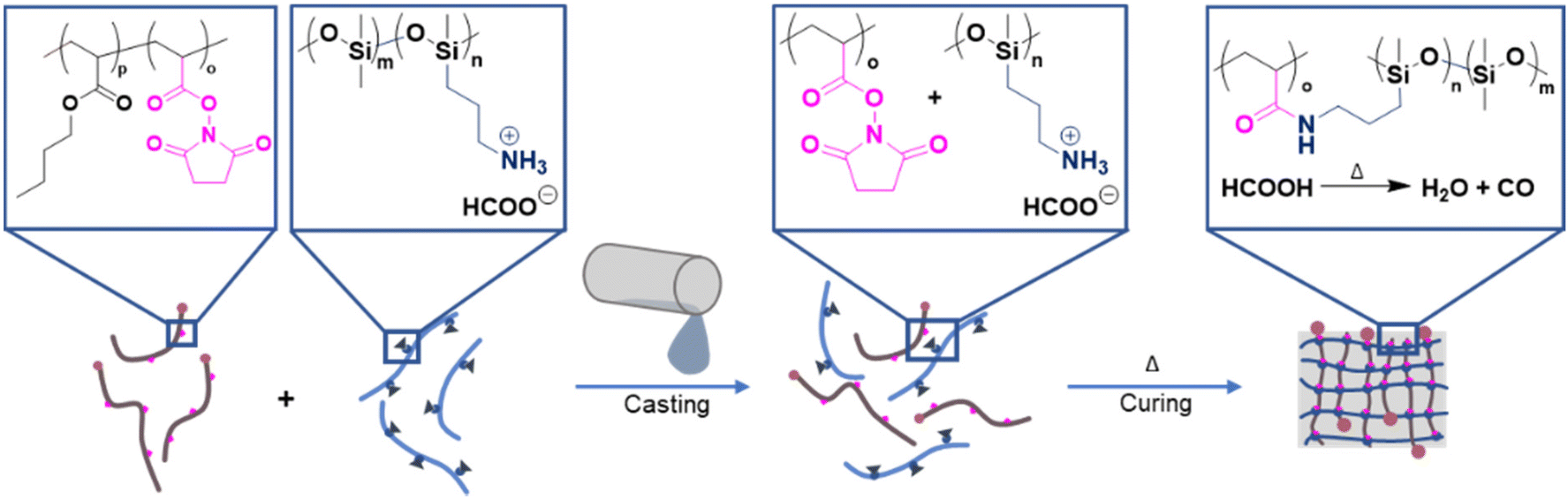 | ||
| Fig. 2 Illustration of the novel stamp preparation process. Protonated 6–7%APMS-co-DMS crosslinks with NAS when mixed and cured. | ||
Thus, the crosslinker was added to the protonated prepolymer and treated at a temperature of 90 °C for curing (Table S2†). To assess an optimized molar ratio of NHS-active ester to amino functionality (in its protonated form), we varied it from 0.25 to 1.6. At a ratio below 0.5 or above 1, incomplete crosslinking was observed, which became obvious as the sample remained sticky (Fig. S3†). When the ratio was kept between these values, the cured stamp was opaque in nature and flexible enough for microcontact printing.
Swelling properties and oPDMS leakage of the stamp
To obtain comprehensive insight into the crosslinking properties of the stamp, we conducted a set of different experiments with various stamps (St1–St14; divided into 14 categories based on different NAS-to-APMS ratios, see Table S2†). The first indication for the crosslinking efficiency was determined by evaluating the stickiness of the material after stamp preparation. For their analyses, the samples were affixed to the lower plate of a microcontact printer (Fig. S4a† shows a computer-aided design drawing of the microcontact printer), and a force of 0.5 N was applied. This force was sustained before being released with a constant force ramp for retraction. As the upper plate was withdrawn, the measured force exhibited negative values (retraction force) from a baseline zero for sticky samples. Conversely, non-sticky samples displayed a consistent line along zero, as displayed in Fig. S4b.† The strength of adhesion directly influenced the retraction force observed during the experiment with stickier samples displaying higher retraction forces. Since the first inspection of the stamps revealed that cross-linking was optimal between the range of 0.5 to 1 (NAS-to-APMS), to obtain more quantitative insight into the results for the optimized ratio, swelling experiments were conducted with representative stamps. Accordingly, different samples were swollen in toluene, which represents a common solvent for both PDMS and acrylate-based prepolymers. After a quick removal of the excessive toluene, thereby placing the stamp in a small plastic tube and removing the supernatant liquid by centrifugation, the relative swelling degree is determined as the mass increase of the stamp after soaking. Subsequent drying of the stamp at elevated temperature and reduced pressure provides access to the gel fraction of the crosslinked material, which is indicative of the non-crosslinked polymer that was removed during the toluene washing. To correlate the swelling properties of the stamp with the characteristics of the crosslinking polymers P1–3, we kept the NAS-to-APMS ratio constant at 0.5 during all experiments. Swelling tests carried out with a stamp prepared with P3 (longest chain) demonstrated lower weight loss than the stamp containing a crosslinker P1 (shortest chain) (Fig. S6†), pointing toward a more efficient crosslinking of the material when longer crosslinking chains are used. The greater weight loss observed for low Mn stamps might be explained by the presence of fewer crosslinking sites in their chains. Nevertheless, the crosslinker with a DP of 10 had superiority in terms of handling during stamp preparation. Considering both ease of handling and weight loss characteristics, stamps prepared with the crosslinker P2 (a DP of 20, St4 and St5, see Table S2†) were prioritized for all further experiments, which provided the optimal trade-off between the fluidity of the crosslinker polymer and the optimal gel properties of the stamp. Next, the effect of the curing temperature was evaluated. For this purpose, initial swelling tests were carried out with sample St4 (containing P2) which was cured at 90 °C (Fig. 3a). The stamp showed a gel fraction of 93.8 ± 0.91% and a swelling degree of 68.18 ± 0.99%. Subsequently, a similar swelling test with another sample, St5, (cured at 110 °C) was performed. It should be noted that no washing step was carried out before the swelling tests. Here, similar characterization values were observed. Afterward, the lost residue during the swelling test was characterized via1H NMR and SEC and assigned to the non-crosslinked prepolymer and crosslinker (shown in Fig. S5a and b†). It should be noted that NHS is present inside the cured stamp, as indicated by 1H NMR characterization of the washing solvents. In that instance, the stamp can be soaked in methanol (MeOH) for 2–3 hours or overnight prior to use, which successfully extracts any unreacted or small molecules that might cause pollution during printing. The treatment also renders the stamp semi-transparent.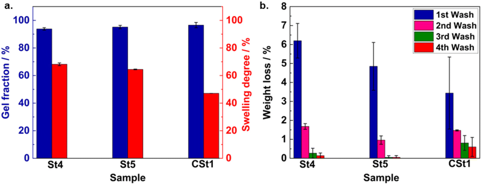 | ||
| Fig. 3 (a) Gel fraction and weight loss (%) of the novel (St4 and 5, cured at 90 °C and 110 °C respectively) and PDMS (CSt1, cured at 110 °C) stamps. Gel fractions are 93.8 ± 0.91%, 95 ± 1.26%, and 96.56 ± 1.9% respectively (St4, St5, and CSt1; determined after the first wash without any prior washing steps). (b) Weight loss profiles of St4 and 5 and CSt1 over 4 weeks. The first wash was considered as the weight loss (%) of the first week directly after production. Weight losses (%) of the first wash are recorded at 6.2 ± 0.91%, 4.25 ± 1.26%, and 3.44 ± 1.9% respectively for St4, St5, and CSt1. The same samples were used for further washing in week 2 to 4 in toluene. | ||
For comparison, a conventional Sylgard PDMS was prepared (refers to CSt1), which uses a prepolymer-to-crosslinker ratio of 10:1 and has been cured at 110 °C. Possessing a similar swelling behavior and a comparable gel fraction right after the preparation (Fig. 3a), both samples differ in their long-term behavior. Accordingly, a major drawback of a PDMS stamp is represented by the fact that Sylgard-based polydimethylsiloxane (PDMS) stamps exhibit a persistent release of oligomeric PDMS. This weight loss is a prevalent occurrence in such stamps and can result in the contamination of the printing substrate.34,35 For quantification of the PDMS release, a long-term experiment was designed to compare the weight loss profiles of the novel and the conventional PDMS-based stamps. In detail, we performed swelling experiments on the previously dried stamp samples St4 and 5 and CSt1 that already underwent the first wash (week 1). The experiments were conducted at weekly intervals for a period of another three weeks to monitor any variations in weight among the samples over time (Fig. 3b). Although the weight loss patterns of the samples indicated that both St4 and St5 experienced a higher initial weight loss (%) directly after production, in comparison with CSt1, a negligible weight loss (%) was observed for the novel stamps in the second week, resulting in no further weight loss after the third and fourth weeks. In contrast, despite exhibiting a low initial weight loss (%) after the first wash, CSt1 demonstrated a consistent trend of weight loss in the second, third, and fourth weeks (Fig. 3b). As a result, the novel stamp has greater potential to mitigate the risk of contaminating the printing surface through the release of contaminants from the stamp. It should be noted that for conventional stamps, thorough washing of the stamp is recommended.35
Mechanical properties
For the characterization of the viscoelastic properties of the materials, we performed dynamic mechanical analyses (DMA) of the cured stamp. For this purpose, we used an oscillatory strain at a frequency of 10 Hz. The behavior of the stamp under compressive force can provide an improved understanding of the printing process, during which the stamp is exposed to a compressive force as well. Since a printing force of no more than 2 N (Newton) is applied to a stamp area of ∼100 mm2, the stamp is supposed to withstand a theoretical stress of around 0.02 MPa. Accordingly, we subjected our stamp (St5) to a dynamic force of Fdyn ∼ 2 N with a temperature ramp up to 150 °C for a duration of 25 min. Fig. 4a reveals that the novel stamp demonstrates an elastic behavior with a storage modulus (E′) of 1.2 MPa at room temperature, which declines as the temperature increases until it reaches a plateau at 0.63 MPa at 146 °C. This indicates that the material possesses adequate elasticity and a low viscous component, as outlined by a low loss modulus (E′′) and a low phase mismatch as characterized by tan δ (for comparison, the viscoelastic behavior of PDMS is shown in Fig. S7a†). In conclusion, the viscoelastic characteristics point mainly toward an elastomeric material in a range relevant to μCP, which renders the material a sufficient elastomer for our method. To obtain further insight into the stamp mechanics, the viscoelastic behavior was also determined in tension mode. There, St5 was exposed to an axial oscillatory force with a frequency of 10 Hz as well. The data reveal a storage modulus E′ of 0.7 MPa at room temperature (Fig. 4b); however, a rise with increasing temperature indicates enhanced crosslinking after a temperature of >130 °C. In analogy to the data obtained in compression mode, a negligible viscous component E′′ (along with a low phase mismatch) is observed too. A corresponding tension profile of PDMS (CSt1) is also shown in Fig. S7b.† We further investigated the tensile properties of St5 and PDMS (CSt1) by measuring uniaxial tensile behavior in a quasi-static manner (Fig. S8†). Our stamp material shows flexibility, with a Young's modulus of 0.68 ± 0.4 MPa, and the highest tensile strength for St5 is observed at 0.14 ± 0.01 MPa (for comparison, the tensile characterization of PDMS is outlined in Fig. S8† as well). However, an elongation at break of 24.1 ± 0.4% is recorded. The elastic properties of the stamp, experiencing a small stress during printing, are therefore well compatible with the experimental printing conditions. | ||
| Fig. 4 Dynamic mechanical analyses of St5 (cured at 110 °C). (a) Compression profile. At 10 Hz with a temperature ramp of 5 K min−1, a dynamic force (Fdyn) ∼ 2 N was applied on a sample size of ∼0.9 cm2. (b) Tension profile (experiments performed at 10 Hz with 5 K min−1 temperature ramp). | ||
These data, all together, reveal the elastic behavior of the produced stamp in both compression and tension modes, which makes it well-compatible with our μCP application.
Surface modification
In order to apply the μCP protocol as described by Akarsu et al.,46 we need to install PTrisAAm brushes at the stamp surface. As the crosslinker polymers P1–4 are prepared by PI-RAFT using xanthate CTAs, the stamps inherit functional CTA moieties at their surfaces, which are directly used for surface grafting (Fig. 5a). For grafting, we exposed the stamps to an aqueous monomer solution, which includes a small amount of the dissolved xanthate CTA as well. Upon irradiating the solution with UV light (365 nm), a polymerization of TrisAAm is induced. The additional CTA in the solution acts, in this context, as a shuttle CTA. Owing to the hydrophobic nature of the stamp, which impedes the penetration of water into the PDMS framework, it can be expected that polymerization occurs exclusively at the stamp surface. It should be noted that determining the accurate brush height, thickness, and grafting density of the formed brushes on a substrate is challenging due to several unknown parameters such as molecular weight (Mn), dispersity, and the degree of polymerization of the formed brushes on that surface.53 However, grafting density can be determined according to the literature using methods such as gravimetric analysis54 or swelling of polymer brushes.55 Those methods are sophisticated and convenient for curved microspheres or planar substrates such as Si wafers.54,55 Due to the soft elastomeric nature of our stamp, the implementation of similar methods to determine brush properties on our stamp is, however, complex. To probe the characteristics of the formed polymer brushes on our stamp, however, contact angle measurements were thus conducted. In addition to that, polymers that formed simultaneously in solution were characterized via SEC. Since CTA-shuttled PI-RAFT polymerization was used, the polymer formed in solution was expected to possess similar properties to the polymer brushes attached to the surface due to the controlled transfer of radicals to different areas of the surface during the reaction.56 The corresponding SEC traces can be found in Fig. S9 and Table S3.† | ||
| Fig. 5 (a) PTrisAAm grafting scheme (CTA in maroon, grafted PTrisAAm in blue). (b) Contact angle measurements before (top) and after (bottom) grafting with PTrisAAM (2 μL Water drop, St4). (c) Mean contact angle before and after grafting PTrisAAm from novel stamps (St4; cured at 90 °C and St5; cured at 110 °C). (d) SEC profile of PTrisAAm in the solution representing the nature of the polymer formed on the stamp's surface due to the shuttle CTA approach. An aqueous solution with 0.3 vol% formic acid and 0.1 M NaCl was used as the SEC eluent (PVP-calibration). | ||
The contact angle measured before grafting averaged 121 ± 6° due to the hydrophobic nature of the stamp material (St4, cured at 90 °C). After PTrisAAm brushes were grafted from the surface, the contact angle significantly decreased to 40 ± 9° (Fig. 5b and c). The number-average molecular weight (Mn) of the polymer simultaneously formed in the solution was determined to be approximately 187 kg mol−1, with a targeted degree of polymerization (DP) of 1500. The dispersity (Đ) was found to be around 6 (Fig. 5d). It should be noted that a high dispersity in polymer brushes can be an advantage, as this increases the contact area of the interface.57 When using the stamp cured at 110 °C (St5), the grafting efficiency was lower, as expressed by a contact angle of 80 ± 22° (Fig. 5c). We explain this result with the inactivation of the xanthate group at this temperature, leading to a less efficient brush formation. At a lower temperature and shorter curing time, the xanthate remains stable producing better results in terms of polymer grafting density from the surface, as it is characterized by a decreased contact angle. Despite performing lower regarding the cross-linking efficiency (as it is characterized by the gel properties), we chose a curing temperature of 90 °C, as it was the best trade-off between the gel characteristics of the stamp and the efficiency to graft polymer brushes from its surface.
Inking and printing
Alkoxy silanes are effective as functionalization agents on oxide surfaces, where they can be subjected to further functionalization,58 which qualifies them to be a suitable ink for our printing method. Due to the trivalent nature of silicon in the structure of APTES, they can be tethered to a polymer offering hydroxy binding sites in their side chains, such as the said PTrisAAm polymer brushes, where they bind in a reversible fashion. Forming stable bonds to hydroxy-terminated oxide surfaces, they can be used to introduce amino-functionalities to the said substrates, which can be used for further functionalization with organic or inorganic molecules (Fig. 6a).59 A similar procedure as we described in our previous study46 was replicated for the novel stamps to attach APTES to the surface-grafted polymer brushes. A concentration of 0.0045 mM (1 mg ml−1 in EtOH) was used for ink attachment to the grafted PTrisAAM polymer. In this study, this concentration was used for all the experiments. The effect of the ink concentration on the attachment to the PTrisAAm polymer was assessed by attaching APTES to the polymer at different molar ratios (APTES-to-PTrisAAm: 0.5, 1, and 1.5) by conducting the conjugation reaction in a solution of the polymer in N,N′-dimethylformamide (DMF). In all cases, the product showed poor solubility in NMR solvents (except D2O, as water promotes hydrolysis forming silanol; 1H NMR spectra shown in Fig. S10c and d†), indicating network formation due to crosslinking between APTES molecules with multiple polymer chains (photographs of the solubility experiment is shown in Fig. S10a and b†). Given the confinement of the polymer chains at the brush matrix, along with the rather high working concentrations of the ink, we assume that there is crosslinking at the polymer brush matrix in the relevant working range. After successful ink attachment, microcontact printing was carried out on a smooth surface for analysis. Possible routes for APTES attachment to the grafted surface, as well as the transfer onto the substrate, are discussed briefly in the ESI section “Ink transfer mechanism”.† To characterize the surface chemistry, an activated surface oxidized Si wafer was selected as the ideal substrate for printing (corresponding Si 2p spectra are shown in Fig. S11a†), and a smooth inked flat stamp (St4) was applied thereon. The transfer of APTES as ink was evaluated by XPS. The characteristic asymmetric peak for N (1s) corresponding to its binding energy at ∼400–405 eV was observed (Fig. 6b; it should be noted that the signals are corrected as they appear downfield shifted, which is a result of an overcompensation from the charge neutralizer of the XPS device). Within this region, signals characteristic of non-protonated (–NH2) and charged amino groups (–NH3+) are found. These results clearly indicate that the amino functions have been transferred from the stamp to the substrate. In addition, elemental analysis of the XPS data of a plasma-treated Si wafer and an APTES-printed Si wafer was compared. The latter shows a trace of nitrogen content, which clearly indicates the APTES transfer to the Si wafer substrate (Fig. 6c), along with significantly enhanced amounts of carbon, also indicating the transfer of APTES. C (1s) signals seen prominently from ∼284 to ∼290 eV (Fig. S11b†) were also investigated, which showed characteristic C–C and C–N regions confirming APTES transfer. Moreover, the curve also resembles the model curves (shown in Fig. S11c and d†), representing characteristic peaks for APTES. | ||
| Fig. 6 (a) Scheme representing APTES ink (in green) attachment to the grafted PTrisAAM polymer (blue) from the novel stamp (St4). ‘*’ denotes that the xanthate group is likely to be cleaved off the polymer in the solution. (b) N (1s) spectra demonstrating APTES transfer to the Si wafer (printing performed with an inked St4). (c) Atomic concentration (%) of elements present on the plasma-treated (left) and APTES-printed Si wafers with St4 (right). | ||
To demonstrate the precision and accuracy of the μCP process on a rough capillary-active surface, we prepared patterned stamps (a light microscopy image of 4 μm stripe patterns is shown in Fig. S12a†) to print on a silica-gel modified glass substrate with a roughness Ra of ∼93 nm (AFM height image is depicted in Fig. S13c†). The accuracy of ink transfer was evaluated by comparative printing experiments performed with a bare stamp and a PTrisAAm-grafted stamp to which non-covalently bound APTES was added as an ink by drop-casting. In comparison, we used a PTrisAAm-grafted stamp inked covalently with APTES through a NaOH-catalysed chemical reaction at elevated temperatures. The printed substrates were labelled with fluorescently active NHS-ester based Alexa 555 dye and analysed by fluorescence microscopy to probe the printing pattern. Evidently shown in Fig. 7c, ink (APTES) transfer to the silica-gel modified glass substrate from the grafted stamp with a covalently attached ink surface is more precise. Please note that the hypothesized mechanism for the ink transfer is outlined in Scheme S1† and discussed in more detail in the ESI.† In Fig. 7a and b, either smeared or incomplete ink transfer is observed, whereas a distinct stripe pattern is observed in Fig. 7c, due to less or no ink smearing. It should be noted that the consistency of the stripe pattern, despite the uneven characteristics of the substrate, can be explained by the soft characteristics of the stamp, which allows a more efficient adaptation to the rough surface topology of the substrate to compensate for uneven surface characteristics. To further show the versatility of the printing process, we used a tailor-made mould, which we created with stereolithographic 3D printing. As outlined in Fig. 8a, the mould possesses structural details in the low μm range, as also shown in the light transmission micrographs (Fig. 8ai and ii). The cast stamp possesses a similar wealth of structural details, which are well preserved after the stamp replication (Fig. 8biii, and Fig. S12b and c†). The stamp, after inking, is subjected to μCP. For visualization of the printing pattern, we exposed the printed area to Alexa 555 dye, as previously mentioned. Noticeable patterns were observed under a fluorescence microscope (Fig. S12d†), using a plasma-activated smooth Si wafer as a substrate. The surface roughness of the smooth Si wafer was measured with AFM, showing an average roughness value, Ra ∼ 0.69 nm (AFM height image shown in Fig. S13a†).
 | ||
| Fig. 7 Fluorescence microscopy images of printed 4 μm stripe patterns (printed with St4) on silica-gel modified glass surfaces. The printed surface was post-labelled with Alexa-555 dye. (a) Printed with a bare stamp inked with APTES (non-covalently attached). Smeared ink transfer onto the substrate was observed. (b) Printed with the grafted stamp inked with APTES (non-covalently attached). Incomplete transfer of 4 μm patterns was seen. (c) Printed with the grafted stamp covalently attached to ink (APTES). Distinct 4 μm patterns were seen. Scale bars are 20 μm. | ||
 | ||
| Fig. 8 (a) CAD of a 3D printed mould with different structural patterns. The zoomed-in area shows light microscopy images of the 3D-printed masters (i and ii). (b) Photography of a patterned stamp. The zoomed-in area ‘iii’ shows the light transmission image of the patterned stamp surface. (c) Fluorescence micrographs of printed patterns on a rough Si wafer. The zoomed-in area on the top row indicates the transfer patterns (the substrate was post-labelled with Alexa555 fluorescence dye). Images are stitched, gamma value (0.38) and brightness corrected on ImageJ. Scale bars are 20 μm. | ||
To demonstrate further the suitability of our method of printing patterns on various rough surfaces, first we used an unpolished side of a Si wafer as a substrate, which possesses a roughness of Ra ∼ 105 nm (AFM height image is shown in Fig. S13b†). Fig. 8c reveals a well-structured pattern transfer from the stamp to the rough wafer surface. Here, also a larger area of printed details is observable. However, due to the coarse characteristics of the prepared mould (average roughness value, Ra ∼ 69 nm; the AFM image is shown in Fig. S14†), transferred structures on the rough Si wafer surface appeared more precise than on the smooth side of the wafer, which can be explained by the fact that the smooth characteristics of the wafer cannot compensate for the roughness of the stamp surface.
As a second surface, a sandblasted glass surface (Fig. S15a and b†), characterized by a higher roughness value (Ra ∼ 314 nm), was selected, as illustrated in the AFM image provided in Fig. S15c.† Ink (APTES) was attached to grafted stamps non-covalently and covalently, following the previously outlined procedure in Fig. 7. As anticipated, the printed substrate obtained from the stamp featuring covalently attached ink exhibits clear patterns (4 μm stripes) compared to the former which shows distorted patterns. Printed patterns are shown in Fig. S15d and e.† This reaffirms the significant influence of the covalent ink-attachment approach and therefore, emphasizes the effectiveness of polymer-brush supported printing.
We also went on to assess the reusability of the stamp. Due to the dynamic nature of the silane bonds, the brush-functionalized stamps should be re-usable. For this purpose, a singular stamp was used for multiple consecutive printing processes (four times, shown in Fig. 9a–d). Between each printing the stamp was washed with acetic acid to remove residual APTES and then subjected again to the inking procedure. As shown in Fig. 9, even after four printing processes, precise patterns are observed without losing structural details.
 | ||
| Fig. 9 Reusability of the stamp (St4) for μCP on a smooth Si wafer surface. (a–d) Fluorescence microscopy images of the first, second, third, and fourth printing using a single stamp respectively. After each printing the stamp was washed with 10% acetic acid solution overnight. The washed stamp was re-inked for successive printing experiments. Images are gamma value (0.38) and brightness corrected on ImageJ. Scale bars are 20 μm. | ||
We are also interested whether one inked stamp can be used for several printing processes, avoiding the re-inking process after each step (Fig. S16†). Using the same stamp, we printed on a smooth Si wafer surface three consecutive times (back-to-back). The patterns after the second printing were less pronounced than the first and nearly faded after the third printing as seen under a fluorescence microscope. Although complete ink transfer does not occur during printing on the first attempt, the potential to perform several printings with a single stamp being inked once can be utilized. These experiments also show that the transfer of the ink does not occur completely after a single printing step.
In all cases, these patterns remain stable even after thorough washing, indicative of the covalent binding of the APTES to the surface.
3. Conclusions
In summary, we developed a novel microcontact printing stamp based on amide crosslinking chemistry. A commercially available reactive amino-containing 6–7%APMS-co-DMS was combined with a xanthate end group-containing polymeric crosslinker, poly(80%butyl acrylate-co-20%N-acryloxysuccinimide), to obtain an elastomeric stamp material via amide coupling. Afterwards, the swelling and the mechanical properties of the stamp were determined. We found that this novel stamp shows a much lower tendency for oligomeric PDMS leakage when compared to conventional stamps, thus overcoming the limitation of conventional stamps that contaminate the substrate area during the μCP process. Our crosslinker was synthesized using photoiniferter RAFT polymerization, which allowed for exclusive access to the xanthate end groups on the surface with an aqueous monomer solution and activation with light. We suspended the stamp in a hydrophilic PTrisAAm monomer solution and illuminated it with UV light for a straightforward grafting process from the surface. This grafted polymer brush was utilized to attach reactive ink namely 3-aminopropyltriethoxysilane (APTES). Therefore, we successfully introduced defined microscale patterns on surface substrates exhibiting high capillary activity and being receptive to silane-based chemistry. Due to the direct availability of xanthate on the stamp surface, polymer grafting is easily achieved and the low oPDMS leakage makes extensive washing unnecessary, thus streamlining the overall procedure drastically. Moreover, by uniting the adaptability of the prepared stamp and the effectiveness of polymer brush-assisted techniques in combatting ink-smearing, this technique is promising in aiding other surface patterning techniques, such as polymer pen lithography (PPL). In conclusion, our polymer-supported μCP method is a promising approach for precise patterning of rough capillary-active surfaces while reducing contamination and maintaining printed pattern fidelity.4. Experimental details
Instrumentation
Materials and methods
A conventional polydimethylsiloxane (PDMS) stamp was prepared from the Sylgard 184 kit. The prepolymer-to-curing agent (10:1, w/w) was mixed, degassed, and cured at 110 °C for 16 h.
| RCF = 1.118 × 10⁻⁵RS2 | (1) |
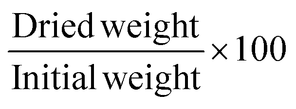
With the mass increase of the swollen stamp, after a quick removal of the excessive toluene, the relative swelling degree was determined. All the samples were dried afterwards in an oven at 60 °C for 5 h. The values were recorded as an average of 3 independent tests. Errors were shown as the standard deviation. Gel fraction (%), swelling degree (%), and weight loss (%) were calculated from the following eqn (2), (3) and (4) respectively.
 | (2) |
 | (3) |
 | (4) |
:1:1, Mili-Q water:hydrogen peroxide:ammonium hydroxide solution (28–30% w/w basis NH3 solution)) at 80 °C for 20 min. The substrate was then washed with Mili-Q water and EtOH. A soft air stream was applied to dry the substrate. The sandblasted part of a microscope slide (Duron Wheaton Kimble, 3 × 1 inch) served as a rough substrate (results shown in Fig. S15†). The substrate was immersed in EtOH and sonicated for 5 min and dried with an air stream. All substrates were plasma treated (100 W, 60 s, 100 air) prior to printing.
Additionally, printing on silica-gel modified glass was performed to investigate the accuracy of the polymer-brush assisted printing method. In this case, a bare stamp and 2 grafted stamps were taken. Stamps prior to treatment were mildly washed by immersing them in MeOH overnight and dried under vacuum (10 mbar) at 60 °C for 1 h.
For non-covalent attachment of the dye, the bare stamp and the grafted stamp were inked with APTES by drop-casting from a 1 mg ml−1 (in EtOH) solution and incubated for 1 h in the dark. Covalent attachment was done as described earlier. The stamps prior to printing were kept together (CVD) with acetic acid (>99%) and Mili-Q water (separate vials) for 2 min in a closed container. Later on, printing was carried out for 10 s at 1 N force with the bare stamp. Printings with grafted stamps with attached non-covalent and covalent dyes were performed for 20 min at 1 N force. The printed substrates were washed with EtOH and post-labelled with Alexa 555 dye for fluorescence imaging. The results are shown in Fig. 7.
Printing on the smooth and rough sides of the Si wafer was done with a force of 1 N and 2 N respectively for 20 min (results shown in Fig. 8). Similar methods and parameters were also followed for printing on the rough sandblasted part of a microscope slide (1 N force).
Multiple printings for investigating the reusability of the stamp were carried out systematically with a single PTrisAAm-grafted groove-patterned stamp. Printing was performed as mentioned before with 1 N force for 20 min. The stamp was exposed to acetic acid and water in a closed container for washing. The stamp was used for printing four times on a smooth Si-wafer. Between each printing step, the stamp was washed with 10% acetic acid (CH3COOH) overnight, dried afterward under vacuum and re-inked (results shown in Fig. 9).
To probe the printing efficiency of an inked stamp, three consecutive printings were carried out using the same stamp. A force of 1 N for 20 min was applied each time (results shown in Fig. S16†).
Conflicts of interest
The authors declare no conflict of interest.Acknowledgements
The authors thank Prof. Alexander Böker of the Fraunhofer Institute for Applied Polymer Research (IAP) in Potsdam for his support. N. P. and M. R. acknowledge the German Research Council (DFG) for financial support (project number 471323994). M. H. gratefully acknowledges funding from the DFG (Emmy-Noether-Program, project number 445804074). The authors acknowledge the company ZUMOLab GmbH (Wesseling, Germany), which manufactured the printing device “ZUMO-MCP (Micro Contact Printer)” that is used in this study. The authors gratefully acknowledge the co-workers of the NMR facility at the Institute of Chemistry, University of Potsdam, including Prof. Dr Heiko Möller, Dr. Matthias Heydenreich, and Angela Krtitschka. Anne-Catherine Lehnen is acknowledged for measuring size-exclusion chromatography. Prof. Dr. Helmut Schlaad and Sascha Prentzel from the Institute of Chemistry (University of Potsdam) are gratefully acknowledged for providing the SEC facility to perform measurements. Monica Heigel and Nicole Fischer are acknowledged for the mechanical characterization of the materials.References
- M. Mirazul Islam, V. Cėpla, C. He, J. Edin, T. Rakickas, K. Kobuch, Ž. Ruželė, W. Bruce Jackson, M. Rafat, C. P. Lohmann, R. Valiokas and M. Griffith, Acta Biomater., 2015, 12, 70 CrossRef CAS PubMed.
- C. D. Eichinger, T. W. Hsiao and V. Hlady, Langmuir, 2012, 28, 2238 CrossRef CAS PubMed.
- E. P. Yalcintas, K. B. Ozutemiz, T. Cetinkaya, L. Dalloro, C. Majidi and O. B. Ozdoganlar, Adv. Funct. Mater., 2019, 29, 1906551 CrossRef CAS.
- D. Li and L. J. Guo, Appl. Phys. Lett., 2006, 88, 063513 CrossRef.
- B. Wang, B. Koo, L. Huang and H. G. Monbouquette, Analyst, 2018, 143, 5008 RSC.
- S.-M. Tsai, T. Goshia, Y.-C. Chen, A. Kagiri, A. Sibal, M.-H. Chiu, A. Gadre, V. Tung and W.-C. Chin, Colloids Surf., B, 2018, 170, 219 CrossRef CAS PubMed.
- Y. Xia and G. M. Whitesides, Annu. Rev. Mater. Sci., 1998, 28, 153 CrossRef CAS.
- M. Geissler, H. Kind, P. Schmidt-Winkel, B. Michel and E. Delamarche, Langmuir, 2003, 19, 6283 CrossRef CAS.
- C. D. James, R. C. Davis, L. Kam, H. G. Craighead, M. Isaacson, J. N. Turner and W. Shain, Langmuir, 1998, 14, 741 CrossRef CAS.
- T. Kaufmann and B. J. Ravoo, Polym. Chem., 2010, 1, 371 RSC.
- A. Kumar and G. M. Whitesides, Appl. Phys. Lett., 1993, 63, 2002 CrossRef CAS.
- N. L. Jeon, R. G. Nuzzo, Y. Xia, M. Mrksich and G. M. Whitesides, Langmuir, 1995, 11, 3024 CrossRef CAS.
- L. Yan, W. T. S. Huck, X.-M. Zhao and G. M. Whitesides, Langmuir, 1999, 15, 1208 CrossRef CAS.
- L. Yan, X.-M. Zhao and G. M. Whitesides, J. Am. Chem. Soc., 1998, 120, 6179 CrossRef CAS.
- L. Zhai, D. W. Laird and R. D. McCullough, Langmuir, 2003, 19, 6492 CrossRef CAS.
- A. Bernard, J. P. Renault, B. Michel, H. R. Bosshard and E. Delamarche, Adv. Mater., 2000, 12, 1067 CrossRef CAS.
- A. Béduer, F. Seichepine, E. Flahaut and C. Vieu, Microelectron. Eng., 2012, 97, 301 CrossRef.
- A. Perl, D. N. Reinhoudt and J. Huskens, Adv. Mater., 2009, 21, 2257 CrossRef CAS.
- W. Bao, D. Liang, M. Zhang, Y. Jiao, L. Wang, L. Cai and J. Li, Prog. Nat. Sci.: Mater. Int., 2017, 27, 669 CrossRef CAS.
- M. J. Madou, Fundamentals of Microfabrication, CRC Press, 2018 Search PubMed.
- T. Lohmüller, D. Aydin, M. Schwieder, C. Morhard, I. Louban, C. Pacholski and J. P. Spatz, Biointerphases, 2011, 6, MR1 CrossRef PubMed.
- G. Liu, S. H. Petrosko, Z. Zheng and C. A. Mirkin, Chem. Rev., 2020, 120, 6009 CrossRef CAS PubMed.
- J. Hyun, S. J. Ahn, W. K. Lee, A. Chilkoti and S. Zauscher, Nano Lett., 2002, 2, 1203 CrossRef CAS.
- L. Stolz Roman, O. Inganäs, T. Granlund, T. Nyberg, M. Svensson, M. R. Andersson and J. C. Hummelen, Adv. Mater., 2000, 12, 189 CrossRef.
- T. F. Didar and M. Tabrizian, Lab Chip, 2012, 12, 4363 RSC.
- R. Kane, Biomaterials, 1999, 20, 2363 CrossRef CAS PubMed.
- D. B. Weibel, A. Lee, M. Mayer, S. F. Brady, D. Bruzewicz, J. Yang, W. R. DiLuzio, J. Clardy and G. M. Whitesides, Langmuir, 2005, 21, 6436 CrossRef CAS PubMed.
- J. Li, L. Xu, S. Kim and A. A. Shestopalov, J. Mater. Chem. C, 2016, 4, 4155 RSC.
- S. J. Clarson and J. A. Semlyen, Siloxane Polymers, Prentice Hall, Englewood Cliffs, N.J, 1993 Search PubMed.
- K. J. Regehr, M. Domenech, J. T. Koepsel, K. C. Carver, S. J. Ellison-Zelski, W. L. Murphy, L. A. Schuler, E. T. Alarid and D. J. Beebe, Lab Chip, 2009, 9, 2132 RSC.
- S.-S. D. Carter, A.-R. Atif, S. Kadekar, I. Lanekoff, H. Engqvist, O. P. Varghese, M. Tenje and G. Mestres, Organs-on-a-Chip, 2020, 2, 100004 CrossRef.
- J. N. Lee, C. Park and G. M. Whitesides, Anal. Chem., 2003, 75, 6544 CrossRef CAS PubMed.
- X. Wang, M. Sperling, M. Reifarth and A. Böker, Small, 2020, 16, 1906721 CrossRef CAS PubMed.
- I. Böhm, A. Lampert, M. Buck, F. Eisert and M. Grunze, Appl. Surf. Sci., 1999, 141, 237 CrossRef.
- D. J. Graham, D. D. Price and B. D. Ratner, Langmuir, 2002, 18, 1518 CrossRef CAS.
- M. Théry and M. Piel, Micropatterning in Cell Biology, Academic Press, Amsterdam, 2014 Search PubMed.
- J. C. Love, L. A. Estroff, J. K. Kriebel, R. G. Nuzzo and G. M. Whitesides, Chem. Rev., 2005, 105, 1103 CrossRef CAS.
- Y. Xia, N. Venkateswaran, D. Qin, J. Tien and G. M. Whitesides, Langmuir, 1998, 14, 363 CrossRef CAS.
- Y. Xia, E. Kim, M. Mrksich and G. M. Whitesides, Chem. Mater., 1996, 8, 601 CrossRef CAS.
- A. Carvalho, M. Geissler, H. Schmid, B. Michel and E. Delamarche, Langmuir, 2002, 18, 2406 CrossRef CAS.
- E. Blinka, K. Loeffler, Y. Hu, A. Gopal, K. Hoshino, K. Lin, X. Liu, M. Ferrari and J. X. J. Zhang, Nanotechnology, 2010, 21, 415302 CrossRef PubMed.
- M. Zimmermann, D. Grigoriev, N. Puretskiy and A. Böker, RSC Adv., 2018, 8, 39241 RSC.
- D. John, M. Zimmermann and A. Böker, Soft Matter, 2018, 14, 3057 RSC.
- M. I. Maksud, M. S. Yusof and M. Mahadi Abdul Jamil, Int. J. Integr. Eng., 2014, 5(3), 36 Search PubMed.
- M. Sperling, M. Reifarth, R. Grobe and A. Böker, Chem. Commun., 2019, 55, 10104 RSC.
- P. Akarsu, R. Grobe, J. Nowaczyk, M. Hartlieb, S. Reinicke, A. Böker, M. Sperling and M. Reifarth, ACS Appl. Polym. Mater., 2021, 3, 2420–2431 CrossRef CAS PubMed.
- P. Akarsu, S. Reinicke, A. Lehnen, M. Bekir, A. Böker, M. Hartlieb and M. Reifarth, Small, 2023, 2301761 CrossRef CAS PubMed.
- G. Liu, M. Hirtz, H. Fuchs and Z. Zheng, Small, 2019, 15, 1900564 CrossRef PubMed.
- A.-C. Lehnen, J. Gurke, A. M. Bapolisi, M. Reifarth, M. Bekir and M. Hartlieb, Chem. Sci., 2023, 14, 593 RSC.
- M. Hartlieb, Macromol. Rapid Commun., 2022, 43, 2100514 CrossRef CAS PubMed.
- A.-C. Lehnen, J. A. M. Kurki and M. Hartlieb, Polym. Chem., 2022, 13, 1537 RSC.
- W. Wang and Q. Zhang, J. Colloid Interface Sci., 2012, 374, 54 CrossRef CAS PubMed.
- L. Michalek, L. Barner and C. Barner-Kowollik, Adv. Mater., 2018, 30, 1706321 CrossRef PubMed.
- Y. Liu, Y. Li, X.-M. Li and T. He, Langmuir, 2013, 29, 15275 CrossRef CAS PubMed.
- S. D. K. Seera and C. W. Pester, ACS Polym. Au, 2023, 3, 428 CrossRef CAS PubMed.
- Z. Zheng, J. Ling and A. H. E. Müller, Macromol. Rapid Commun., 2014, 35, 234 CrossRef CAS PubMed.
- M. Romio, B. Grob, L. Trachsel, A. Mattarei, G. Morgese, S. N. Ramakrishna, F. Niccolai, E. Guazzelli, C. Paradisi, E. Martinelli, N. D. Spencer and E. M. Benetti, J. Am. Chem. Soc., 2021, 143, 19067 CrossRef CAS PubMed.
- L. Wang, U. S. Schubert and S. Hoeppener, Chem. Soc. Rev., 2021, 50, 6507 RSC.
- H. Li, J. Zhang, X. Zhou, G. Lu, Z. Yin, G. Li, T. Wu, F. Boey, S. S. Venkatraman and H. Zhang, Langmuir, 2010, 26, 5603 CrossRef CAS PubMed.
- D. Goswami, S. K. Medda and G. De, ACS Appl. Mater. Interfaces, 2011, 3, 3440 CrossRef CAS PubMed.
Footnote |
| † Electronic supplementary information (ESI) available: NMR spectra, SEC data, mechanical data, light and fluorescence microscopy images, and AFM height images of samples. See DOI: https://doi.org/10.1039/d3py01036h |
| This journal is © The Royal Society of Chemistry 2024 |