
 Open Access Article
 This Open Access Article is licensed under a
 Creative Commons Attribution 3.0 Unported Licence
A negative photoconductivity photodetector based on two-dimensional Nb3Cl8†
Bom
Lee‡
a,
Xiaojie
Zhang‡
a,
Jinsu
Kang
a,
Byung Joo
Jeong
a,
Sooheon
Cho
a,
Kyung Hwan
Choi
b,
Jiho
Jeon
b,
Sang Hoon
Lee
a,
Dahoon
Kim
a,
Yeong Hyeop
Kim
a,
Ji-Hee
Kim
 *c,
Hak Ki
Yu
*d and
Jae-Young
Choi
*ab
*c,
Hak Ki
Yu
*d and
Jae-Young
Choi
*ab
aSchool of Advanced Materials Science & Engineering, Sungkyunkwan University, Suwon 16419, Korea. E-mail: choi@skku.edu
bSKKU Advanced Institute of Nanotechnology (SAINT), Sungkyunkwan University, Suwon 16419, Korea
cDepartment of Physics, Pusan National University, Busan 46241, Republic of Korea. E-mail: kimjihee@pusan.ac.kr
dDepartment of Materials Science and Engineering & Department of Energy Systems Research, Ajou University, Suwon 16499, Korea. E-mail: hakkiyu@ajou.ac.kr
First published on 7th October 2024
Abstract
Negative photoconductivity (NPC)-based photodetectors offer a new direction for energy-efficient photodetection technologies, featuring low energy consumption and high responsivity. Two-dimensional (2D) materials are particularly promising for implementing NPC due to their large surface area, abundant surface states, and tunable bandgap properties. In this context, 2D Nb3Cl8, with its unique kagome lattice structure and broad absorption spectrum, has attracted considerable interest. Notably, metal halides such as Nb3Cl8 demonstrate significant potential as NPC materials due to their low anionic and cationic bonding strength, which allows for the formation of vacancy defects with high probability. However, the NPC characteristics of Nb3Cl8 have not been thoroughly investigated. In this study, we fabricated field-effect transistors (FETs) using Nb3Cl8 single crystals synthesized via chemical vapor transport (CVT). These devices exhibited an electron mobility of 4.24 × 10⁻³ cm2 V−1 s−1 and a high Ion/Ioff ratio of 1.42 × 10⁴. Notably, Nb3Cl8-based photodetectors demonstrated consistent NPC behavior across a wide wavelength range of 400–1050 nm, with a high responsivity of 156.82 mA W−1 at 400 nm. We propose that the trapping effect due to defect levels within the bandgap is the primary cause of this NPC phenomenon. The present findings reveal the unique photodetector properties of Nb3Cl8 and highlight its promise in energy-efficient photodetectors and various optoelectronic applications.
Introduction
The development of low-power photodetectors has garnered significant attention in recent years, driven by their potential to extend battery life and reduce operational costs across various applications.1,2 Among the diverse strategies explored to achieve low power consumption in these devices, research on negative photoconductivity (NPC) has emerged as a particularly promising approach.3–5 NPC is characterized by a decrease in electrical conductivity upon light exposure, in contrast to the conventional positive photoconductivity (PPC) phenomenon where conductivity increases under illumination. This unique feature of NPC, where light-induced current changes oppose the dark current, offers an improved signal-to-noise ratio (SNR) by facilitating better discrimination between the signal and background noise. Consequently, NPC-based photodetectors could enable more accurate and reliable data collection in complex sensing environments.6,7 The NPC effect stems from various mechanisms, including trap states induced by surface-adsorbed gas molecules,8,9 energy band alignment through heterostructures,10–12 and surface plasmon effects.13 Despite extensive research, the NPC mechanism in semiconductors remains unclear due to the complex interplay of these multiple factors. Notably, NPC mechanisms attributed to heterojunctions or atmospheric molecule adsorption introduce numerous variables from a device fabrication and control perspective, making interpretation challenging. Therefore, there is significant value in conducting research focused on interpreting NPC through defect level control within single materials.Two-dimensional (2D) materials are particularly promising for implementing NPC due to their high surface-to-volume ratio, which facilitates defect control, and their potential for band engineering through various material combinations.14–16 However, to date, most research utilizing 2D materials has focused on NPC mechanisms arising from heterojunctions16–18 and molecular adsorption.19–21 Therefore, selecting and synthesizing a 2D material that allows for the optimization of surface (including edge) defects and then studying NPC in this single material hold significant importance. Considering these factors, our research has focused on the Nb3X8 family of materials (where X = Cl, Br, or I) as promising candidates. Nb3X8 compounds possess a 2D structure, resulting in a high surface-to-volume ratio, and the utilization of edge sites facilitates the formation of defect levels.22–24 Moreover, metal halides such as Nb3X8 can form vacancy defects due to their weak anionic and cationic bond strengths.25 Among these materials, Nb3Cl8, which possesses an appropriate semiconductor bandgap (∼1 eV), broad-spectrum light absorption properties, biocompatibility, and ferromagnetism, is expected to be a promising candidate for various photonic applications, including nonvolatile memory, biophotonics, and optospintronics, when combined with its NPC behavior.26–31
In this study, we synthesized Nb3Cl8 single crystals using the chemical vapor transport (CVT) method and conducted a comprehensive investigation of their physical, electrical, and optical properties. We observed NPC behavior in Nb3Cl8, which we attribute to the trapping effect caused by defect levels within the bandgap. Our fabricated devices demonstrate notable NPC performance, providing insights into this phenomenon in a single-material 2D system. These findings not only elucidate the intriguing NPC behavior of Nb3Cl8 but also open promising avenues for its application in various optoelectronic devices, contributing to the broader understanding of NPC in 2D materials.
Results and discussion
To investigate the NPC performance of Nb3Cl8, we synthesized high-quality single crystals and conducted comprehensive characterization studies. As depicted in Fig. 1a, Nb3Cl8 crystallizes in the trigonal space group P![[3 with combining macron]](https://www.rsc.org/images/entities/char_0033_0304.gif) m1 (no. 164), exhibiting a layered structure parallel to the (001) plane with a theoretical monolayer thickness of approximately 0.6 nm, composed of NbCl6 octahedra. Three NbCl6 octahedra share four Cl atoms, forming a triangle-like unit with 60° rotational symmetry. Each angle of the triangle shares four Cl atoms connected with the adjacent two units, creating a special arrangement of Nb atoms that forms the kagome structure of Nb3Cl8.26,32 To synthesize Nb3Cl8 single crystals, we employed a solid-state reaction method using CVT with high-purity niobium (Nb, 99.99%, Alfa Aesar) and niobium(V) chloride (NbCl5, 99.95%, Alfa Aesar) as precursors. Fig. 1b presents the X-ray powder diffraction (XRD) analysis of Nb3Cl8 single crystals and powder samples. By comparing with ICSD-257110 (ICSD release 2021.2),30,33 the phase was identified as Nb3Cl8. The sharp diffraction peaks observed in the XRD pattern indicate that the samples exhibit high crystallinity. However, due to the random orientation of numerous fine grains in the powder sample, multiple diffraction peaks are visible in the powder Nb3Cl8 XRD pattern. In contrast, the prominent peaks of the single crystal Nb3Cl8 appear at around 14.52° and 44.30°, corresponding to the (002) and (006) planes, respectively, indicating that a preferred orientation of Nb3Cl8 crystal growth was along the (00l) direction, which is characteristic of single crystals. The inset in Fig. 1b shows an optical image of the synthesized Nb3Cl8 with its hexagonal crystal structure, revealing a well-developed two-dimensional layered structure, further confirming the successful growth of Nb3Cl8 single crystals on the centimeter scale. We verified the distribution uniformity of the three elements by energy dispersive spectroscopy (EDS) mapping, as shown in Fig. 1c. EDS analysis confirmed that the stoichiometric ratio of Nb and Cl was close to 3
m1 (no. 164), exhibiting a layered structure parallel to the (001) plane with a theoretical monolayer thickness of approximately 0.6 nm, composed of NbCl6 octahedra. Three NbCl6 octahedra share four Cl atoms, forming a triangle-like unit with 60° rotational symmetry. Each angle of the triangle shares four Cl atoms connected with the adjacent two units, creating a special arrangement of Nb atoms that forms the kagome structure of Nb3Cl8.26,32 To synthesize Nb3Cl8 single crystals, we employed a solid-state reaction method using CVT with high-purity niobium (Nb, 99.99%, Alfa Aesar) and niobium(V) chloride (NbCl5, 99.95%, Alfa Aesar) as precursors. Fig. 1b presents the X-ray powder diffraction (XRD) analysis of Nb3Cl8 single crystals and powder samples. By comparing with ICSD-257110 (ICSD release 2021.2),30,33 the phase was identified as Nb3Cl8. The sharp diffraction peaks observed in the XRD pattern indicate that the samples exhibit high crystallinity. However, due to the random orientation of numerous fine grains in the powder sample, multiple diffraction peaks are visible in the powder Nb3Cl8 XRD pattern. In contrast, the prominent peaks of the single crystal Nb3Cl8 appear at around 14.52° and 44.30°, corresponding to the (002) and (006) planes, respectively, indicating that a preferred orientation of Nb3Cl8 crystal growth was along the (00l) direction, which is characteristic of single crystals. The inset in Fig. 1b shows an optical image of the synthesized Nb3Cl8 with its hexagonal crystal structure, revealing a well-developed two-dimensional layered structure, further confirming the successful growth of Nb3Cl8 single crystals on the centimeter scale. We verified the distribution uniformity of the three elements by energy dispersive spectroscopy (EDS) mapping, as shown in Fig. 1c. EDS analysis confirmed that the stoichiometric ratio of Nb and Cl was close to 3![[thin space (1/6-em)]](https://www.rsc.org/images/entities/char_2009.gif) :8 (Fig. 1d). Furthermore, we confirmed the 2D layered structure of Nb3Cl8 through scanning electron microscopy (SEM) images (inset of Fig. 1d). Given that the layers are bound by van der Waals forces, Nb3Cl8 can be easily exfoliated down to nanometer size using tape, as detailed in the Experimental section. We performed atomic force microscopy (AFM) to observe the micromechanical exfoliation results. Fig. 1e shows the morphology of exfoliated Nb3Cl8, which forms a 2D nanosheet. Fig. 1f presents the height profile along the red line in Fig. 1e, indicating that we successfully obtained layered Nb3Cl8 with a thickness of 30.4 nm, demonstrating the favorable exfoliating performance of Nb3Cl8. To further evaluate the phonon dynamics and structural information of the Nb3Cl8 crystal, we conducted Raman spectroscopy measurements. Using a 633 nm laser, we observed 15 Raman peaks in the 100–400 cm−1 range, as shown in Fig. 1g. 12 of the observed peaks are in complete agreement with the experimental results reported in ref. 34. However, three additional Eg peaks were observed at 100.94 cm−1, 185.22 cm−1, and 276.09 cm−1. Based on the computational results, these Eg peaks correspond to the intrinsic vibrational modes of the material, indicating a distinct advantage in crystallinity for the synthesized material. The absence of Eg peaks is typically associated with low crystallinity, crystal disorder, or defects.35 The presence of these Eg peaks in our synthesized Nb3Cl8 suggests a more ordered crystal structure with significantly reduced defects and disorder. Furthermore, the emergence of these Eg peaks may also reflect an increase in grain size or a reduction in grain boundary effects, further indicating an improvement in the internal structural uniformity. It is also possible that the synthesized Nb3Cl8 exhibits a more stable and highly symmetric crystalline phase. Therefore, our synthesized Nb3Cl8 demonstrates superior crystallinity, structural order, and phase stability compared to the material reported in the reference. Additionally, to assess the long-term stability of the material, we conducted XRD measurements after exposing the Nb3Cl8 crystals to ambient air for 90 days. As shown in Fig. S1,† we observed no significant changes in the XRD peaks, confirming the excellent material stability of our Nb3Cl8 crystals over time.
:8 (Fig. 1d). Furthermore, we confirmed the 2D layered structure of Nb3Cl8 through scanning electron microscopy (SEM) images (inset of Fig. 1d). Given that the layers are bound by van der Waals forces, Nb3Cl8 can be easily exfoliated down to nanometer size using tape, as detailed in the Experimental section. We performed atomic force microscopy (AFM) to observe the micromechanical exfoliation results. Fig. 1e shows the morphology of exfoliated Nb3Cl8, which forms a 2D nanosheet. Fig. 1f presents the height profile along the red line in Fig. 1e, indicating that we successfully obtained layered Nb3Cl8 with a thickness of 30.4 nm, demonstrating the favorable exfoliating performance of Nb3Cl8. To further evaluate the phonon dynamics and structural information of the Nb3Cl8 crystal, we conducted Raman spectroscopy measurements. Using a 633 nm laser, we observed 15 Raman peaks in the 100–400 cm−1 range, as shown in Fig. 1g. 12 of the observed peaks are in complete agreement with the experimental results reported in ref. 34. However, three additional Eg peaks were observed at 100.94 cm−1, 185.22 cm−1, and 276.09 cm−1. Based on the computational results, these Eg peaks correspond to the intrinsic vibrational modes of the material, indicating a distinct advantage in crystallinity for the synthesized material. The absence of Eg peaks is typically associated with low crystallinity, crystal disorder, or defects.35 The presence of these Eg peaks in our synthesized Nb3Cl8 suggests a more ordered crystal structure with significantly reduced defects and disorder. Furthermore, the emergence of these Eg peaks may also reflect an increase in grain size or a reduction in grain boundary effects, further indicating an improvement in the internal structural uniformity. It is also possible that the synthesized Nb3Cl8 exhibits a more stable and highly symmetric crystalline phase. Therefore, our synthesized Nb3Cl8 demonstrates superior crystallinity, structural order, and phase stability compared to the material reported in the reference. Additionally, to assess the long-term stability of the material, we conducted XRD measurements after exposing the Nb3Cl8 crystals to ambient air for 90 days. As shown in Fig. S1,† we observed no significant changes in the XRD peaks, confirming the excellent material stability of our Nb3Cl8 crystals over time.
 | ||
| Fig. 1 Characterization of Nb3Cl8. (a) Schematic illustration of the 2D Nb3Cl8 crystal structure. (b) XRD pattern of Nb3Cl8 single crystals and powder samples, consistent with the calculated results. The inset shows the experimentally obtained single crystal. (c) EDS elemental mapping images of Nb and Cl in the Nb3Cl8 crystal. (d) Atomic ratio of Nb and Cl elements determined by EDS from multiple points. The inset shows an SEM image of the Nb3Cl8 crystal. (e) AFM image of mechanically exfoliated Nb3Cl8. (f) Height profile of the exfoliated Nb3Cl8 shown by the red line in (e). (g) Raman spectrum of Nb3Cl8 measured at an excitation wavelength of 633 nm. | ||
The atomic structure of Nb3Cl8 was further characterized by transmission electron microscopy (TEM). Fig. 2a shows a low-magnification TEM image of the Nb3Cl8 nanosheet, while Fig. 2b presents a high-resolution TEM image of the area indicated in Fig. 2a. To enhance the clarity of the TEM images, a masking function in the Gatan Microscopy Suite software was applied, resulting in Fig. 2c. The fast Fourier transform (FFT) pattern shown in the inset of Fig. 2c exhibits a hexagonal distribution of reciprocal lattice points, consistent with the Pm1 space group symmetry. This symmetry contains one threefold rotational axis, one inversion center, and three mirror symmetry planes that divide the crystal into six equivalent directions, confirming the periodicity of the Nb3Cl8 crystal.32 The white circles shown in the inset for the FFT pattern represent the (011) and (013) crystal planes, corresponding to the [100] zone axis. The measured distance between the (011) crystal planes is 0.54 nm, which aligns well with our simulated crystal structure results.
 | ||
| Fig. 2 TEM characterization of the Nb3Cl8 crystal. (a) TEM image of the Nb3Cl8 crystal at low magnification. (b) High-resolution TEM image of the Nb3Cl8 crystal. (c) Enlarged HRTEM image of the Nb3Cl8 crystal, with the corresponding fast-Fourier transform (FFT) images shown in the inset. | ||
To evaluate the optical properties of Nb3Cl8, we first sought to characterize its basic electrical properties. This preliminary electrical characterization serves several important purposes: it confirms the semiconductor nature of the material and establishes a baseline for understanding how light interaction might affect these properties. For these electrical properties, we exfoliated Nb3Cl8 with a thickness of 8.72 nm onto the SiO2/Si substrate. Fig. 3a and b show a schematic illustration and SEM image, respectively, of the Nb3Cl8-based FET device structure. The device was fabricated using a photolithography process, with Cr/Au (5/50 nm) deposited via e-beam evaporation to form the conducting electrodes. A 100 nm-thick SiO2 layer served as the dielectric, and a highly doped silicon substrate was utilized as the back gate. Fig. 3c shows the output characteristics (Ids–Vds) of the Nb3Cl8 FET, measured at room temperature for various gate biases (Vg) ranging from −40 to 40 V in 10 V increments. The device exhibits typical n-type semiconductor behavior, with the drain current increasing proportionally as Vg increases in the positive Vds region (0 to 1 V).36 Notably, the clear linear behavior observed across all gate biases indicates excellent ohmic contact between the channel layer and metal electrodes, suggesting low contact resistance in our fabricated device. This ohmic behavior is crucial for efficient charge injection and extraction, which is essential for optimal device performance.37 Furthermore, Fig. 3d presents the transfer characteristic of the Nb3Cl8 FET as a function of Vg from −50 to 50 V at a drain voltage (Vds) of 1 V. The device exhibits n-type semiconductor behavior in both logarithmic (black line) and linear (red line) scales.36,37 From these measurements, we calculated the field-effect mobility (μ) to be 4.24 × 10⁻³ cm2 V−1 s−1 and the Ion/Ioff current ratio to be 1.42 × 10⁴, indicating good switching behavior. Furthermore, as shown in Fig. S2,† after 90 days of ambient exposure, the device maintained consistent mobility and an Ion/Ioff current ratio, indicating good long-term stability of Nb3Cl8-based FETs. The field-effect mobility was calculated using eqn (1):
| μ = [L/(W × COX × Vds)] × (dIds/dVg) | (1) |
 | ||
| Fig. 3 Electronic properties of few-layer Nb3Cl8. (a) Schematic illustration and (b) the SEM image of the Nb3Cl8 FET with a thickness of 8.72 nm, as measured by AFM. (c) Output characteristics (Ids–Vds) at various gate voltages ranging from −40 to 40 V at a 10 V interval. (d) Transfer characteristics (Ids–Vg) of Nb3Cl8 nanosheets, obtained by sweeping the gate voltage from −50 to 50 V at a fixed Vds of 1 V. The data are presented in both linear (blue) and logarithmic (black) scales. | ||
To verify the NPC performance of Nb3Cl8 and investigate its optoelectronic characteristics across a broad spectral range, we fabricated photodetectors using Nb3Cl8 flakes. Unlike most previously reported NPC materials that exhibit this behavior only at specific wavelengths, we aimed to explore Nb3Cl8's potential for NPC over an extended spectrum. We first performed absorption spectrum analysis using an ultraviolet (UV)-visible-near-infrared (NIR) microspectrophotometer (Fig. 4a). The results revealed multiple absorption peaks spanning from the UV to the NIR regions, indicating that Nb3Cl8 interacts with light across a wide range of wavelengths. From the Tauc plot (inset of Fig. 4a), we determined the optical band gap of Nb3Cl8 to be 1.38 eV. Notably, we observed an additional peak at 1000 nm (1.23 eV), which lies within the band gap and may originate from defects or edge states.26 These defect levels can act as recombination centers, reducing the number of free charge carriers and decreasing conductivity under illumination.39 To illustrate this mechanism, we have included a detailed band diagram in Fig. S3,† which clearly demonstrates the NPC process in Nb3Cl8. Therefore, the presence of defects in Nb3Cl8 provides clear evidence for the potential occurrence of NPC across a wide spectral range. Furthermore, this trapping effect by a trap site is corroborated by the hysteresis observed in the device characteristics, as shown in Fig. S4.†28 To further support this hypothesis, we performed gate voltage sweeps under dark and light conditions, as shown in Fig. S5.† The observed power-dependent gate voltage threshold shift provides strong evidence that the origin of NPC is indeed related to electron trapping.5
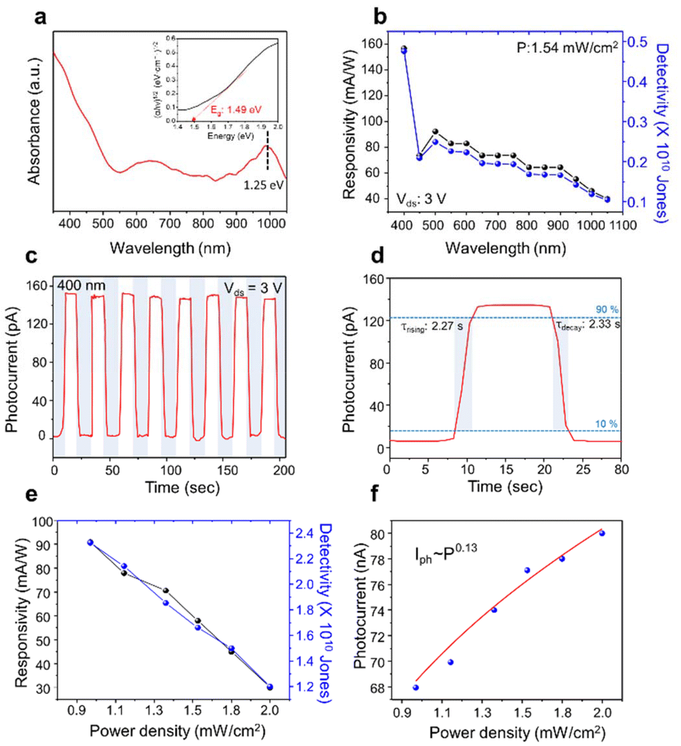 | ||
| Fig. 4 Optical properties of few-layer Nb3Cl8. (a) UV-visible-NIR absorption spectra and the Tauc plot of Nb3Cl8 used to determine the band gap. (b) Wavelength dependent responsivity and detectivity at Vds = 3 V and power density = 1.54 mW cm−2. (c) Time-resolved photoresponse and (d) rising and decay curves of Nb3Cl8 at Vds = 3 V under 400 nm light with a power density of 1.54 mW cm−2. (e) Responsivity and detectivity at varying power densities of 400 nm light, measured at a Vds = 3 V. (f) Photocurrent as a function of illumination intensity at Vds = 3 V and 400 nm light. | ||
Based on the broad absorption profile shown in Fig. 4a, we conducted comprehensive optoelectronic characterization studies. We performed Ids–Vds measurements (Fig. S6†) and time-resolved photoresponse analyses (Fig. S7†) across various wavelengths to investigate the device's performance and NPC behavior. These measurements, ranging from 450 nm to 1050 nm in 50 nm steps, demonstrate consistent NPC behavior throughout the tested spectrum. From these time-resolved photocurrent data, we extracted the responsivity and detectivity values for each wavelength. Fig. 4b summarizes the results of this comprehensive analysis, presenting the wavelength-dependent responsivity and detectivity characteristics of the photodetector device.40 Additionally, we calculated the external quantum efficiency (EQE) for various wavelengths, which is included in Fig. S8† to provide a more comprehensive understanding of the device's performance. The key parameters of responsivity (Rλ), detectivity (D*), and EQE were calculated using the following equations: Rλ = Iph/(Popt × A), where Iph is the photocurrent, Popt is the incident optical power, and A is the effective area of the detector; D* = RλA1/2/(2eId)1/2, where e is the elementary charge and Id is the dark current; and EQE = hcRλ/(eλ), where h is Planck's constant, c is the speed of light in a vacuum, and λ is the excitation wavelength. Our analysis confirms that the device exhibits the highest performance at 400 nm while maintaining significant NPC response across the entire tested range. The time-dependent current response of the Nb3Cl8 FET under 400 nm illumination, shown in Fig. 4c, clearly demonstrates NPC behavior. To evaluate the long-term stability of the photoresponse, we conducted repeated measurements over 30 cycles, as shown in Fig. S9.† The results demonstrate consistent photodetector performance throughout the cycles, indicating excellent stability of our Nb3Cl8-based device under prolonged optical operation. Furthermore, to investigate the possibility of NPC performance originating from oxygen molecule adsorption and desorption, we conducted tests under vacuum conditions, as shown in Fig. S10;† the persistent NPC behavior observed under these conditions suggests that molecular adsorption is not the primary cause of the NPC performance in our Nb3Cl8-based device. Fig. 4d presents a detailed view of the photoresponse dynamics, focusing on the rising and decay regions. Analysis of these regions reveals response times of approximately 1.45 ms for the rising phase and 1.40 ms for the decay phase.41Fig. 4e and f demonstrate the optical performance at different power densities. As shown in Fig. 4e, responsivity and detectivity decrease with increasing excitation power, possibly due to more frequent carrier recombination and shorter carrier lifetimes at higher illumination intensities.42Fig. 4f presents the relationship between photocurrent and light intensity, which follows a power law, Iph ≈ Pm,42,43 where m is an exponent indicating the intensity-dependent photo response, primarily influenced by trap states on the device's surface. To further optimize our device performance, we conducted a comprehensive study of the photodetection properties of Nb3Cl8 nanoflakes as a function of thickness. As illustrated in Fig. S11,† the responsivity exhibits a strong dependence on the Nb3Cl8 nanoflake thickness. Our results reveal that the maximum responsivity is achieved at an optimal thickness of 8.72 nm. This optimal performance can be attributed to the minimization of dark current at this specific thickness, which significantly enhances the overall photoresponse characteristics. This thickness-dependent behavior aligns with previous studies on other 2D materials, suggesting a common trend in optimizing 2D material-based photodetectors.44,45 Finally, we have conducted a comprehensive comparison between our Nb3Cl8-based NPC device and other reported 2D material-based NPCs, as illustrated in Table S1.† This study emphasizes the importance of exploring new materials for NPC applications, highlighting Nb3Cl8 as a promising candidate that opens up new avenues for research and development in the field of energy-efficient photodetectors.
Conclusions
In summary, we have successfully investigated the NPC phenomenon in the 2D material Nb3Cl8. Nb3Cl8 single crystals were synthesized via the CVT method and comprehensively characterized using XRD, EDS, SEM, AFM, Raman spectroscopy, and TEM. We fabricated FETs using exfoliated Nb3Cl8, demonstrating n-type semiconductor behavior with an electron mobility of 4.24 × 10⁻³ cm2 V−1 s−1 and a high Ion/Ioff ratio of 1.42 × 10⁴. Notably, our optical characterization confirmed consistent NPC behavior under illumination across a broad spectrum from 400 to 1050 nm, with the highest responsivity of 156.82 mA W−1 observed at 400 nm. The primary mechanism driving the NPC phenomenon in Nb3Cl8 is attributed to the trapping effect due to defect levels within the bandgap. This study not only provides valuable insights into the intriguing NPC behavior of Nb3Cl8 but also opens up promising avenues for exploiting its unique properties in various optoelectronic applications, particularly in the development of energy-efficient and highly responsive photodetectors.Experimental section
Synthesis of Nb3Cl8 single crystals
Single crystals of Nb3Cl8 were prepared by a solid-state reaction method using high purity niobium (Nb, 99.99%, Alfa Aesar) and niobium(V) chloride (NbCl5, 99.95%, Alfa Aesar). 0.5 g stoichiometric amounts of Nb and NbCl5 were sealed in an evacuated 12 cm long quartz tube, which was placed in a furnace at 800 °C for 7 days with a temperature increase of 100 °C h−1, and then cooled to room temperature naturally. After the reaction, 2D flake-shape single crystals of cm-scale Nb3Cl8 were collected.Material characterization
Powder X-ray diffraction (XRD, D8 Advance, Bruker) was performed using Cu Kα radiation (λ = 0.154 nm) to determine the Nb3Cl8 phase. A field-emission scanning electron microscope (FE-SEM, JSM-7600F, Jeol) and an energy dispersive spectrometer (EDS) attached to the FE-SEM were used for morphological analyses at an accelerating voltage of 15 kV and a beam current of ≈10 μA. Atomic force microscopy (AFM, Park Systems, NX 10) was operated in the non-contact mode for the topographic analysis of the mechanically exfoliated Nb3Cl8 on the SiO2/Si substrates. Raman spectroscopy (Raman, LabRAM HR Evolution, Horiba) was conducted using a 633 nm laser. Transmission electron microscopy (TEM, JEM-200F, Jeol) and TEM mapping were performed with an accelerating voltage of 200 kV to investigate the crystal orientation and nanostructure of Nb3Cl8. The sample was prepared via drop-casting onto a copper grid coated with an amorphous carbon layer. A UV-visible-NIR microspectrophotometer (20/20 PVTM, CRAIC Technologies) was used to study the absorption of Nb3Cl8 in the 200–1050 nm range.Mechanical exfoliation
Nb3Cl8 bulk crystals were mechanically exfoliated onto cleaned SiO2 (100 nm)/Si substrates using adhesive tape. Devices were fabricated using standard photolithography techniques. An AZ5214E photoresist was spin-coated at 4000 rpm for 40 seconds, followed by pre-baking at 110 °C for 1 min. UV exposure and development processes were used to form electrode patterns. Finally, Cr/Au (5/50 nm) electrodes were deposited by electron beam evaporation under high vacuum conditions (below 5 × 10⁻⁷ mbar). This process completed the device fabrication for electrical characterization.Measurements of electrical and optical properties
The semiconductor properties of the fabricated Nb3Cl8 FETs were evaluated under controlled vacuum conditions (approximately 1 × 10⁻³ mbar). For precise electrical measurements, an advanced probe station (M6VC, MSTECH) was employed. The transfer and output characteristics of the devices were analyzed using a high-precision semiconductor parameter analyzer (Model 4200 SCS, Keithley Instruments Inc.).To investigate the photoresponse of the devices, a monochromatic light source system featuring a xenon lamp (MonoRa-200, Dongwoo Optron Co. Ltd) was employed. This setup allowed for the generation of specific wavelengths across a broad spectrum. Transient photocurrent measurements were conducted using a probe station in conjunction with the semiconductor parameter analyzer, enabling the precise temporal analysis of the device's response to light stimuli.
Author contributions
B. L. and X. Z. contributed equally to this work. J. K., K. H. C. and J. J. supported the synthesis and analysis. B. J. J., S. C. and S. H. L. supported the measurements and analysis. D. K. and Y. H. K. supported data curation and analysis. J.-H. K., H. K. Y. and J.-Y. C. supervised the whole project.Data availability
The data supporting this article have been included as part of the ESI.†Conflicts of interest
There are no conflicts to declare.Acknowledgements
This research was supported by the Basic Science Research Program through the National Research Foundation of Korea, funded by the Korean Government (MSIT, RS-2023-00208311), and the KIST Institutional Program (project no. 2E31854-22-066) from the Korea Institute of Science and Technology.References
- J. R. Nasr, N. Simonson, A. Oberoi, M. W. Horn, J. A. Robinson and S. Das, ACS Nano, 2020, 14, 15440–15449 CrossRef CAS.
- H. Qiao, Z. Huang, X. Ren, S. Liu, Y. Zhang, X. Qi and H. Zhang, Adv. Opt. Mater., 2020, 8, 1900765 CrossRef CAS.
- B. Cui, Y. Xing, K. Niu, J. Han, H. Ma, W. Lv, T. Lei, B. Wang and Z. Zeng, J. Sci.: Adv. Mater. Devices, 2022, 7, 100484 CAS.
- H. J. Kim, K. J. Lee, J. Park, G. H. Shin, H. Park, K. Yu and S.-Y. Choi, ACS Appl. Mater. Interfaces, 2020, 12, 38563–38569 CrossRef CAS.
- Y. Yang, X. Peng, H.-S. Kim, T. Kim, S. Jeon, H. K. Kang, W. Choi, J. Song, Y.-J. Doh and D. Yu, Nano Lett., 2015, 15, 5875–5882 CrossRef CAS.
- N. K. Tailor, C. A. Aranda, M. Saliba and S. Satapathi, ACS Mater. Lett., 2022, 4, 2298–2320 CrossRef CAS.
- L. Wang, H. Wang, J. Liu, Y. Wang, H. Shao, W. Li, M. Yi, H. Ling, L. Xie and W. Huang, Adv. Mater., 2024, 2403538 CrossRef CAS.
- Y. Liu, P. Fu, Y. Yin, Y. Peng, W. Yang, G. Zhao, W. Wang, W. Zhou and D. Tang, Nanoscale Res. Lett., 2019, 14, 1–7 CrossRef.
- S. Zhuang, Y. Chen, Y. Xia, N. Tang, X. Xu, J. Hu and Z. Chen, AIP Adv., 2016, 6, 045214 Search PubMed.
- J. Xu, Y. J. Song, J.-H. Park and S. Lee, Solid-State Electron., 2018, 144, 86–89 CrossRef CAS.
- Y. Lee, H. Kim, S. Kim, D. Whang and J. H. Cho, ACS Appl. Mater. Interfaces, 2019, 11, 23474–23481 CrossRef CAS.
- B. Liu, C. You, C. Zhao, G. Shen, Y. Liu, Y. Li, H. Yan and Y. Zhang, Chin. Opt. Lett., 2019, 17, 20002 CrossRef.
- Q. Wang, Y. Tu, T. Ichii, T. Utsunomiya, H. Sugimura, L. Hao, R. Wang and X. He, Nanoscale, 2017, 9, 14703–14709 RSC.
- R. R. Nair, P. Blake, A. N. Grigorenko, K. S. Novoselov, T. J. Booth, T. Stauber, N. M. R. Peres and A. K. Geim, Science, 2008, 320, 1308 CrossRef CAS.
- C. Lee, X. Wei, J. W. Kysar and J. Hone, Science, 2008, 321, 385–388 CrossRef CAS.
- W. Zheng, B. Zheng, C. Yan, Y. Liu, X. Sun, Z. Qi, T. Yang, Y. Jiang, W. Huang and P. Fan, Adv. Sci., 2019, 6, 1802204 CrossRef.
- S. Ghosh, A. Varghese, H. Jawa, Y. Yin, N. V. Medhekar and S. Lodha, ACS Nano, 2022, 16, 4578–4587 CrossRef CAS.
- A. Vardi, G. Bahir, S. E. Schacham, P. K. Kandaswamy and E. Monroy, J. Appl. Phys., 2010, 108 Search PubMed.
- Z. Zhang, S. Wang, C. Liu, R. Xie, W. Hu and P. Zhou, Nat. Nanotechnol., 2022, 17, 27–32 CrossRef CAS.
- X. Zhang, D. Meng, Z. Tang, D. Hu and D. Ma, J. Mater. Sci.: Mater. Electron., 2016, 27, 11463–11469 CrossRef CAS.
- A. Grillo, E. Faella, A. Pelella, F. Giubileo, L. Ansari, F. Gity, P. K. Hurley, N. McEvoy and A. Di Bartolomeo, Adv. Funct. Mater., 2021, 31, 2105722 CrossRef CAS.
- Q. Yue, Z. Shao, S. Chang and J. Li, Nanoscale Res. Lett., 2013, 8, 1–7 CrossRef.
- F. Schedin, A. K. Geim, S. V. Morozov, E. W. Hill, P. Blake, M. I. Katsnelson and K. S. Novoselov, Nat. Mater., 2007, 6, 652–655 CrossRef CAS.
- A. Shokri and N. Salami, Sens. Actuators, B, 2016, 236, 378–385 CrossRef CAS.
- A. Walsh, D. O. Scanlon, S. Chen, X. G. Gong and S. Wei, Angew. Chem., 2015, 127, 1811–1814 CrossRef.
- Z. Sun, H. Zhou, C. Wang, S. Kumar, D. Geng, S. Yue, X. Han, Y. Haraguchi, K. Shimada and P. Cheng, Nano Lett., 2022, 22, 4596–4602 CrossRef CAS.
- A. Bouhmouche, A. Jabar, I. Rhrissi and R. Moubah, Mater. Sci. Semicond. Process., 2024, 175, 108238 CrossRef CAS.
- J.-G. Chen, G.-M. Cao, Q. Liu, P. Meng, Z. Liu and F.-C. Liu, Rare Met., 2022, 41, 325–332 CrossRef CAS.
- J. Yoon, E. Lesne, K. Sklarek, J. Sheckelton, C. Pasco, S. S. P. Parkin, T. M. McQueen and M. N. Ali, J. Phys.: Condens. Matter, 2020, 32, 304004 CrossRef CAS.
- Y. Haraguchi, C. Michioka, M. Ishikawa, Y. Nakano, H. Yamochi, H. Ueda and K. Yoshimura, Inorg. Chem., 2017, 56, 3483–3488 CrossRef CAS.
- B. Mortazavi, X. Zhuang and T. Rabczuk, Appl. Phys. A, 2022, 128, 934 CrossRef CAS.
- G. J. Miller, J. Alloys Compd., 1995, 217, 5–12 CrossRef CAS.
- D. Zagorac, H. Müller, S. Ruehl, J. Zagorac and S. Rehme, J. Appl. Crystallogr., 2019, 52, 918–925 CrossRef CAS.
- D. A. Jeff, F. Gonzalez, K. Harrison, Y. Zhao, T. Fernando, S. Regmi, Z. Liu, H. R. Gutierrez, M. Neupane and J. Yang, 2D Mater., 2023, 10, 45030 CrossRef CAS.
- A. C. Ferrari and J. Robertson, Phys. Rev. B: Condens. Matter Mater. Phys., 2000, 61, 14095 CrossRef CAS.
- B. J. Jeong, B. Lee, K. H. Choi, D. Sung, S. Ghods, J. Lee, J. Jeon, S. Cho, S. H. Lee and B. J. Kim, Nano Lett., 2023, 23, 6269–6275 CrossRef CAS.
- B. Lee, B. J. Jeong, K. H. Choi, S. Cho, J. Jeon, J. Kang, X. Zhang, H.-S. Bang, H.-S. Oh and J.-H. Lee, ACS Appl. Mater. Interfaces, 2023, 15, 42891–42899 CrossRef CAS.
- X. Liu, J. Liu, L. Y. Antipina, J. Hu, C. Yue, A. M. Sanchez, P. B. Sorokin, Z. Mao and J. Wei, Nano Lett., 2016, 16, 6188–6195 CrossRef CAS.
- L. Xie, L. Guo, W. Yu, T. Kang, R. K. Zheng and K. Zhang, Nanotechnology, 2018, 29, 464002 CrossRef.
- Q. Liu, B. Cook, M. Gong, Y. Gong, D. Ewing, M. Casper, A. Stramel and J. Wu, ACS Appl. Mater. Interfaces, 2017, 9, 12728–12733 CrossRef CAS.
- B. Lee, T. Nasir, S. Cho, M. Jung, B. J. Kim, S. H. Lee, H. E. Jang, J. Kang, H. K. Yu and J. Y. Choi, IEEE Sens. J., 2024, 24, 6038–6044 CAS.
- F. Wang, T. Gao, Q. Zhang, Z. Y. Hu, B. Jin, L. Li, X. Zhou, H. Li, G. Van Tendeloo and T. Zhai, Adv. Mater., 2019, 31, 1–10 CAS.
- X. Zhou, L. Gan, W. Tian, Q. Zhang, S. Jin, H. Li, Y. Bando, D. Golberg and T. Zhai, Adv. Mater., 2015, 27, 8035–8041 CrossRef CAS.
- H. Yu, Y. Wang, H. Zeng, Z. Cao, Q. Zhang, L. Gao, M. Hong, X. Wei, Y. Zheng and Z. Zhang, ACS Nano, 2024, 18, 18073–18081 Search PubMed.
- X. Jia, C. Tang, R. Pan, Y. Long, C. Gu and J. Li, ACS Appl. Mater. Interfaces, 2018, 10, 18073–18081 CrossRef CAS.
Footnotes |
| † Electronic supplementary information (ESI) available. See DOI: https://doi.org/10.1039/d4nr03376k |
| ‡ These authors contributed equally to this work. |
| This journal is © The Royal Society of Chemistry 2024 |