
 Open Access Article
 This Open Access Article is licensed under a Creative Commons Attribution-Non Commercial 3.0 Unported Licence
Visualizing localized nematic states in twisted double bilayer graphene†
Zhen-Yu
Wang‡
a,
Jia-Jun
Ma‡
a,
Qianqian
Chen‡
b,
Kefan
Wu
a,
Shuigang
Xu
cd,
Qing
Dai
 e,
Zheng
Zhu
bf,
Jindong
Ren
*e,
Hong-Jun
Gao
af and
Xiao
Lin
*af
e,
Zheng
Zhu
bf,
Jindong
Ren
*e,
Hong-Jun
Gao
af and
Xiao
Lin
*af
aInstitute of Physics and University of Chinese Academy of Sciences, Chinese Academy of Sciences, Beijing 100190, China. E-mail: xlin@ucas.ac.cn
bKavli Institute for Theoretical Sciences, University of Chinese Academy of Sciences, Beijing 100190, China
cKey Laboratory for Quantum Materials of Zhejiang Province, School of Science, Westlake University, Hangzhou 310024, China
dInstitute of Natural Sciences, Westlake Institute for Advanced Study, Hangzhou 310024, China
eCAS Key Laboratory of Nanophotonic Materials and Devices, CAS Key Laboratory of Standardization and Measurement for Nano-Technology, National Center for Nanoscience and Technology, Beijing 100190, China. E-mail: renjd@nanoctr.cn
fCAS Center for Excellence in Topological Quantum Computation, University of Chinese Academy of Sciences, Beijing, 100190, China
First published on 10th September 2024
Abstract
Direct visualization of the states originating from electron–electron interactions is of great importance for engineering the surface and interfacial properties of graphene-based quantum materials. For instance, the rotational symmetry breaking or nematic phase inferred from spectroscopic imaging has confirmed the existence of correlated states in a wide range of moiré materials. Here, we study the atomic-scale spatial distributions and symmetry of wave functions in gate-tunable twisted double bilayer graphene by employing scanning tunneling microscopy/spectroscopy and continuum model calculations. A series of spectroscopic imaging analyses are used to identify dominant symmetry breaking of the emergent states. Interestingly, in non-integer hole fillings, a completely new localized electronic state with rotational symmetry breaking is observed on the left side of the valence flat band. The degree of anisotropy is found to increase from the conduction flat band through the valence flat band to the new state. Our results provide an essential microscopic insight into the flat band and its adjacent state for a full understanding of their electric field response in twisted graphene systems.
 Jindong Ren | Prof. Jindong Ren is a Professor of Experimental Physics and Chemistry at the National Center for Nanoscience and Technology, China. His research spans nanoscale science and nanotechnology, with a focus on on-surface precision chemistry, interfacial charge transfer, and the optoelectronic properties of low-dimensional materials. Prof. Ren is at the forefront of integrating advanced techniques such as scanning tunneling microscopy/spectroscopy, non-contact atomic force microscopy, and X-ray photoelectron spectroscopy. His pioneering work in atomic-level surface positioning, angstrom-scale spatial structure analysis, millielectronvolt-level electronic state characterization, and deca-Newton mechanical resolution is driving innovation in the regulation of nanoscale physical and chemical properties. |
Introduction
Various physical phenomena have been discovered in graphitic moiré systems, where two atomically thin van der Waals (vdW) layers are stacked with a misalignment, such as insulating and superconducting phases,1–8 orbital ferromagnets9–11 and correlated Chern insulators.12–17 These prominent electronic states could be attributed to the creation of the isolated low-energy flat band,18,19 whose bandwidth is comparable to or even smaller than the Coulomb interactions. Indeed, different from magic angle twisted bilayer graphene (MATBG), recent studies have implied a much wider range of twisted angles (0.84°–1.53°) to realize this flat band in twisted double bilayer graphene (tDBLG), which thus can provide an identical platform to study the novel physics in moiré vdW heterostructures.1,3,20,21 For example, Zhang et al. have shown that a correlation-induced gap is delocalized throughout different stacking sites.22 Rubio-Verdú et al. have reported that an interaction-driven electronic nematic phase at the scale of a moiré lattice can be observed at doping values between 0.3 and 0.7 of the filling in the conduction flat band.23 However, the spatial distributions of wave functions under different electric fields are still not comprehensively understood and their symmetry information, which is extremely important for understanding correlated physics in tDBLG, also remains unclear.In this work, using scanning tunneling microscopy and spectroscopy (STM/STS) measurements, we characterize the evolution of the band structure in tDBLG at various back gate voltages. We compare the energy gap in three typical inequivalent stacking configurations and find an asymmetric fashion related to the polarity of gate voltage. At positive polarity, the STS measurements show a correlated state featuring splitting bands when the conduction flat band is half-filled. The anisotropy magnitudes of these two sub-bands are totally different based on the anisotropy quantification technique.24 Moreover, a new electronic state, localized in the ABAB and ABCA stacking regions, appears under certain negative electric fields and exhibits the strongest rotational symmetry breaking compared to its neighboring flat bands.
Results and discussion
Fig. 1c shows a representative STM topographic image of a tDBLG sample measured in a gated device (schematic and optical images are shown in Fig. 1a and b). The relative twist angle between bilayers will yield a moiré superlattice. As indicated by the black dashed quadrilateral, the unit cell is given by L1 ≈ 10.7 nm and L2 = L3 ≈ 11.1 nm. The twist angle, θ, can be estimated from the moiré period, L, through the equation , where a = 0.246 nm is the lattice constant of graphene.22 Accordingly, the twisted angle is θ ≈ 1.28°, while the strain is around 0.1%.24 Within the moiré pattern, three distinct regions can be classified based on their different heights. The bright spots correspond to ABBC stacking. In this area, each upper layer atom is directly located above the lower layer atoms. Besides, each bright spot is surrounded by six relatively darker regions consisting of alternating ABCA and ABAB stacking25 (see Fig. 1c).
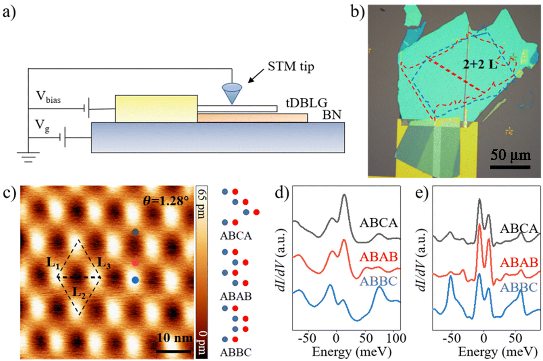 | ||
| Fig. 1 Basic characterization of tDBLG. (a and b) STM measurement configuration and optical image of the device. The blue-colored region corresponds to the lower bilayer graphene (BN graphene in (a)), whereas the red-colored region represents the upper bilayer graphene (tDBLG graphene in (a)). (c) STM topography of tDBLG with a twist angle of 1.28°. Setpoint: 1 V, 100 pA. The right part shows three distinct stacking orders. (d) STS measurements in three different stacking regions. The black, red and blue filled spots in panel (c) denote the stacking regions ABCA, ABAB and ABBC, respectively. Setpoint: −0.2 V, 100 pA. (e) Continuum model calculations of the LDOS on ABCA, ABAB, and ABBC sites. | ||
To investigate the intrinsic local density of states (LDOS) of tDBLG and explore novel correlation phenomena in the twisted multilayer graphene systems, the spatially resolved dI/dV spectra are obtained in these three inequivalent stacking areas at the charge neutrality point where zero doping and zero displacement field are applied in the sample. Fig. 1d shows a series of asymmetric double peaks with a pronounced dip feature around the Fermi level. The experimental observation is consistent with a more thorough study based on continuum model calculations,26 as shown in Fig. 1e, which reveals the flat bands and their lateral distribution. We define the peaks as the valence flat band (VFB) and conduction flat band (CFB) in the following text. Their spatial dependence is discussed based on the spectra at three high-symmetry sites. Both the VFB and the CFB manifest exactly the same energy position. Different from MATBG, where flat bands are concentrated in AA stacking regions,5,24,27 the observed bands here are non-localized and spread over the entire moiré superlattice. Apart from the flat bands, remote bands on the hole and electron sides are also observed, which are labeled as RCB (the remote conduction band) and RVB (the remote valence band), respectively. The excellent agreement between the experimental observations and theoretical calculations, as shown in Fig. 1d and e, indicates that the low-energy bands in the tDBLG can be well captured by the continuum model.
Our observation of the non-localized flat bands immediately raises one important question concerning the spatial distribution of electronic states after applying different back gate voltages to the sample. Different from MATBG, the band structure of tDBLG manifests an apparent change as we tune the back gate voltage.23 The color map of dI/dV spectra in the ABBC region (Fig. 2a), ranging from highly p-doped to highly n-doped, shows that the four peaks move to the left, which means that the bands’ filling evolves from empty to full. Indeed, three band gaps can be identified, i.e. the gaps between the RVB and VFB (ΔV), the VFB and CFB (ΔVC), and the CFB and RCB (ΔC), in each spectrum. In the case of ΔV and ΔC, their values decrease continuously when increasing the gate voltage |Vg| (Fig. S1†), revealing that the band structure in tDBLG is sensitive to the external electric field. For the gap ΔVC, Fig. 2b indicates its dependence on the back-gate voltage and presents a clearly asymmetric behavior with respect to the polarity of Vg. For example, the measured ΔVC starts to increase monotonically when the applied negative back gate voltage exceeds −40 V. However, in the positive range, it changes immediately once electrons are doped in the sample. Indeed, such a phenomenon is caused by the polarizing effect of the electric field,28 which changes the spatial distribution of electronic states across the different atomic layers of tDBLG.
 | ||
| Fig. 2 Gate-dependent spectroscopy in three stacking regions. (a and b) Gate-dependent dI/dV spectra in ABBC regions over the voltage range of −65 V to 60 V. The energy difference between the VFB and CFB at different gate voltages for the three stacking orders is shown in panel (b). Based on ABBC, the trace of ABAB (ABCA) is shifted by 15 meV for clarity. (c and d) dI/dV maps and (e and f) the corresponding simulations of the tDBLG region obtained at the energy of the VFB measured at Vg = −30 V (top) and Vg = 30 V (bottom). The dashed lines in panels (c) and (d) are inferred from the corresponding STM images shown in Fig. S3.† Setpoint for all panels: −0.2 V, 100 pA. | ||
To prove this point, we calculate the LDOS distribution at different layers acquired over the carrier filling ranging from empty to full doping (see Fig. S2).† Obviously, the LDOS distributes symmetrically between the top and bottom layers at zero electric field. After applying Vg, it becomes asymmetric between layers 1 and 4, and the other two layers remain unchanged. We should note that, due to the STM geometry, the measured STS signal is dominated by the top layer. We thus compare our experimental dI/dV maps with theoretical calculations of the top layer at the flat bands’ voltage. For example, Fig. 2e and f present the simulated images at the energy of the VFB measured at Vg = ±30 V, which fits the experimental dI/dV maps well (see Fig. 2c and d). The VFB is mostly localized on the ABBC stacking site, while the CFB is localized on the ABAB stacking site at negative back gate voltage. However, after switching the polarity of gate voltage to positive, the LDOS distribution of the VFB (CFB) changes to ABAB (ABCA), respectively.
Indeed, the CFB splits into two subbands when it moves into the Fermi level (Fig. 3a). We denote the lower subband and upper subband as CFB− (left) and CFB+ (right) in the following text. Such a phenomenon cannot be simply explained by single particle calculations, which means electron–electron interactions should be considered. Similar to previous work,27 we can obtain the local filling of the subband from the spectral weight transfer:  (see the inset of Fig. 3a). The lower subband loses spectral weight, while the upper subband gains weight with decreasing doping. In particular, the splitting peaks can be easily distinguished when Vg is tuned at around 30 V where half electron filling (≈0.5ns) occurs in the moiré systems. We thus measure the spectral weight dependence of the lateral position29 across the ABBC region and calculate the spatial charge redistribution at Vg = 30 V. The local charge can be inferred from the peak areas ALB and ATOT along three different directions, and the obtained results associated with the position are shown in Fig. 3c. Following this analysis, a parabolic curve, indicating the spatial charge distribution, opens downwards, and the center of the ABBC stacking region exhibits the largest value, revealing a non-uniform charge distribution around the ABBC region.
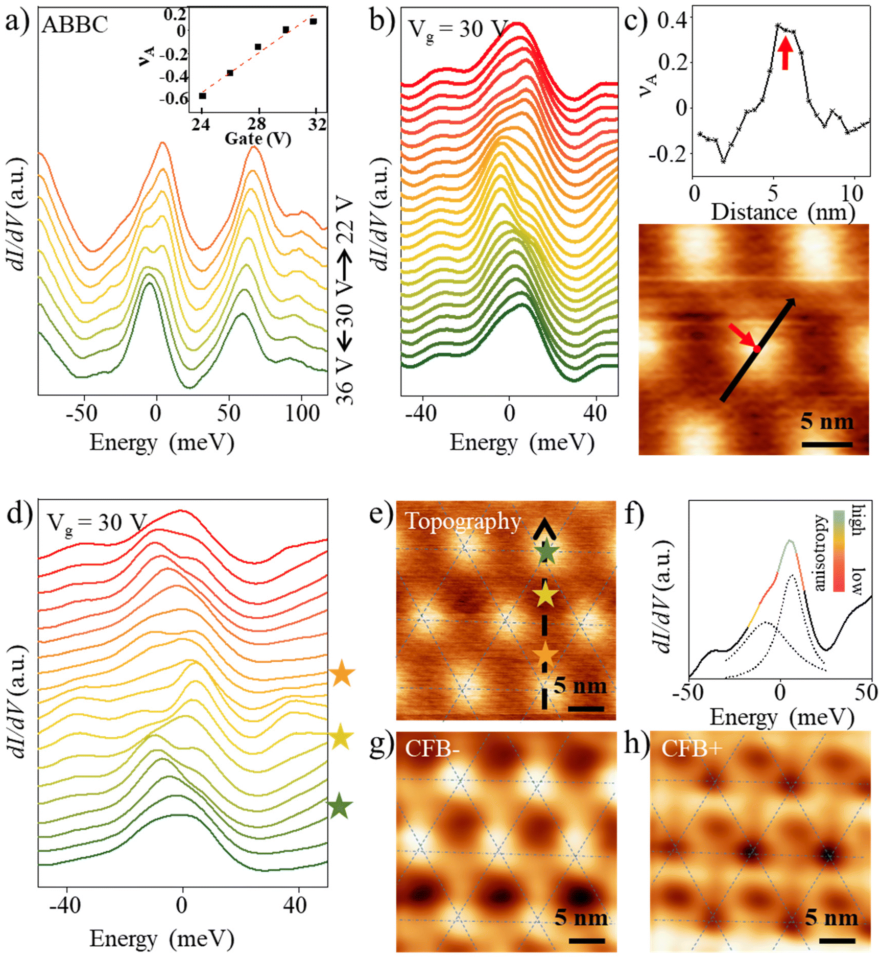 | ||
| Fig. 3 Emergent correlated insulating states at half filling of the conduction band. (a) Gate-dependent spectroscopy in the ABBC stacking region for 22 V < Vg < 36 V. The inset shows the gate-voltage dependence of the filling fraction within the flat band extracted from panel (a). The dotted line shows the fitting line. (b) dI/dV spectra along the black solid arrow in panel (c) across the ABBC stacking region at Vg = 30 V. (c) Position dependence of the filling fraction inferred from panel (b). The site with the largest filling is marked by the red arrow. (d) Spatially resolved spectra along the unit cell marked in panel (e) at Vg = 30 V. (f) The averaged curve over ABBC, ABCA and ABAB sites, and the superimposed color scale represent the anisotropy values. The dashed curves denote contributions from the CFB. (g and h) Spatially dependent DOS distributions at the energy of CFB− and CFB+ at Vg = 30 V. Setpoint for all panels: −0.2 V, 100 pA. | ||
We extend the lateral dependence measurement across the entire moiré superlattice and observe the splitting dI/dV curves with LDOS reduction at v ≈ 2, as shown in Fig. 3d. The correlated states in our tDBLG are spatially extended, consistent with previous reports22 in the same system but with a different twisted angle. To better understand the spatial distributions of the correlated states, we further obtain the dI/dV maps over several moiré superlattices at the energy of CFB− and CFB+ (see Fig. 3g and h). For CFB−, the LDOS is mainly distributed in the ABBC stacking regions, in line with the above results. As for CFB+, the LDOS in the ABCA region shows the largest magnitude, and this area is surrounded by six dim circles. tDBLG is characterized by a D3 symmetry point group, consisting of an out-of-plane three-fold rotational axis (C3) and three in-plane two-fold rotational axes (C′2). We quantify the degree of C3 symmetry breaking by comparing differences between an STS map at a specific energy and its counterpart rotated at 120°, which should be identical in C3 symmetry.23 As illustrated in Fig. 3g, we first isolate a single Wigner–Seitz cell from the triangular lattice formed by the LDOS in tDBLG. Then, we calculate the energy-dependent anisotropy24via the spatial LDOS profiles of the Wigner–Seitz cells rotated by 120° and 240°, respectively. Different from MATBG, which shows highly enhanced anisotropy at energies around the correlated insulating gap,24 a dip is observed in a narrow region of energy around the Fermi level in the tDBLG system, as evidenced by the anisotropy curves shown in Fig. 3f.
Meanwhile, the anisotropy at CFB+ is larger than that at CFB−. We remark that the experimentally observed spatially extended correlated state at v ≈ 2 suggests that an integer quantum Hall ferromagnet state could be a promising candidate state, where spontaneous polarization could be driven by the anisotropic Coulomb interaction,30 thus giving rise to the reduction of LDOS at the Fermi level, though the systematical characterization of such a correlated state still calls for future study via distinct measurements.1,3
In addition to the correlated insulating phase at positive Vg, we also investigates the behavior of the tDBLG system in a negative voltage range, i.e., hole doping, and found a new electronic state on the left side of the VFB. Fig. 4a shows the gate-dependent spectra in the ABCA region. A new peak (labeled as VB) appears in the range of −50 V to −37.5 V and should originate from the displacement field induced by the gate electrode.23 To further characterize its spatial distribution, which is essential for a full understanding of the novel state in the twisted multilayer graphene systems, the site-resolved LDOS spectra are acquired at a negative voltage, for example at Vg = −45 V, and shown in Fig. 4b. Interestingly, this new state is localized in the ABAB and ABCA regions, and the value between these two peaks reaches the maximum in the region between ABAB and ABCA stacking (see Fig. 4d). To reveal the underlying symmetry of the emergent electronic state (VB) and flat bands (VFB and CFB) at the negative back gate voltage, we perform energy-dependent STS mapping (see Fig. 4c). Remarkably, unidirectional stripes are observed at the mapped energy of the VB, revealing the symmetry breaking of C3. The detailed analysis of anisotropy24 is shown in Fig. 4d, and the value is strongest in the energy region around the VB. Meanwhile, for the other two flat bands, the anisotropy value at the VFB is much larger than that at the CFB.
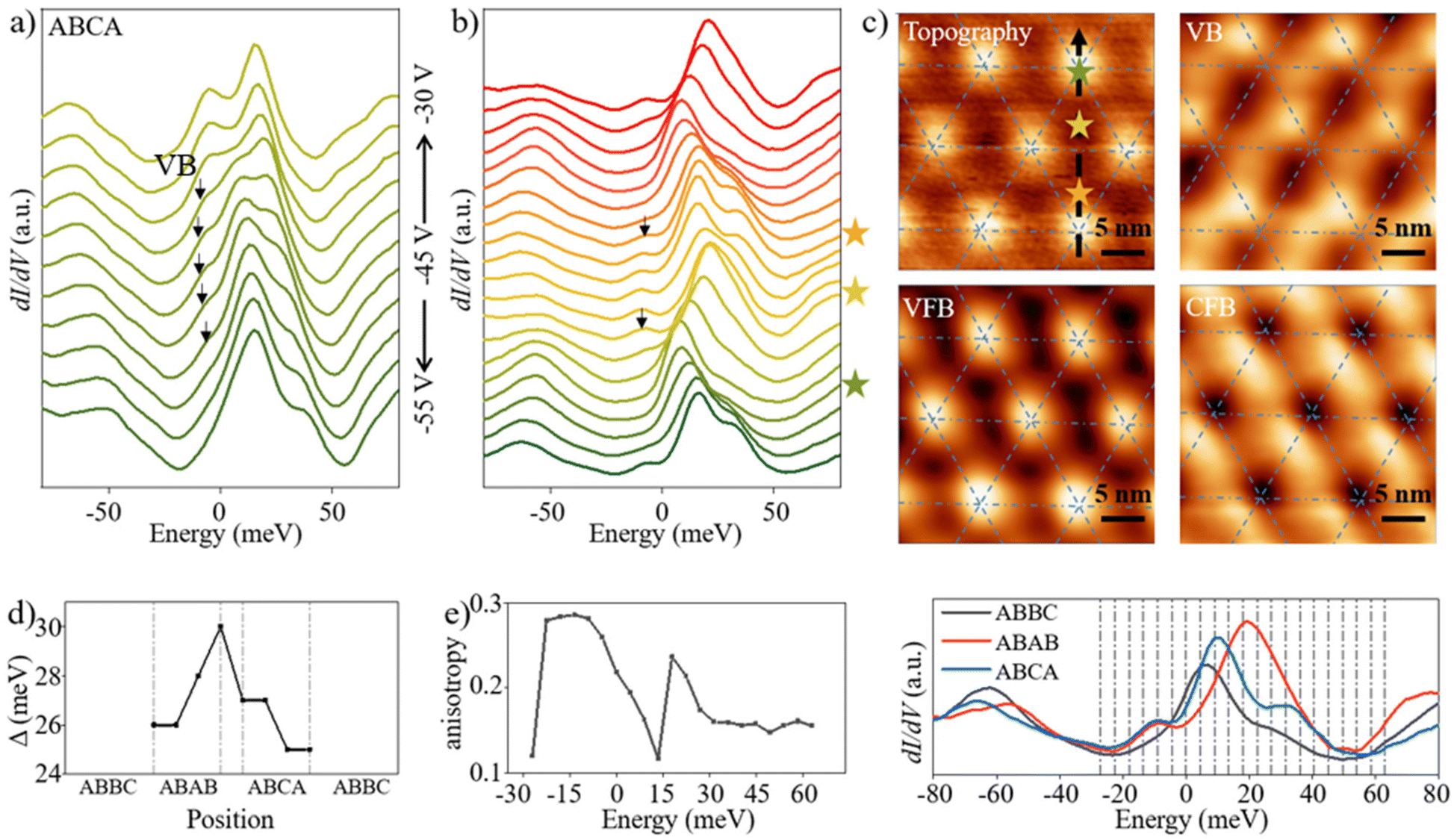 | ||
| Fig. 4 Emergent electronic states at negative Vg. (a) Gate-dependent spectroscopy in the ABCA stacking region for −30 V < Vg < −55 V. The black arrows denote the position of the VB. (b) dI/dV spectra along the dashed line in the right part across the whole unit cell at Vg = −45 V. (c) Spatially dependent DOS distributions at the energy of the VB, VFB and CFB at Vg = −45 V. (d) The energy interval between the VB and VFB in three stacking regions. (e) Left part: the measured anisotropy values obtained at different energies marked in the right image. Right part: the dI/dV spectra obtained in the three typical regions at Vg = −45 V. Setpoint for all panels: −0.2 V, 100 pA. | ||
Conclusions
In conclusion, STM/STS measurements present the spatial distribution of Coulomb interaction driven insulating states and displacement field induced electronic states in gate-tunable twisted double bilayer graphene devices. For all inequivalent stacking areas inside the moiré unit, we find that the relationship between the band structure and the back-gate voltage reveals a distinctly asymmetric behavior with respect to the polarity of Vg. We note, in particular, that for a positive electric field, the CFB splits into two subbands when it moves into the Fermi level. Among them, the upper one exhibits a larger anisotropy. The STM observations indicate a spatially delocalized correlated state with strong anisotropy. Furthermore, we demonstrate for the first time the investigation of a new sharp density of states around the VFB after applying a certain negative electric field. The spatial measurements show that it is localized in the ABAB and ABCA regions, while its anisotropy value is larger than that of the VFB. Therefore, our work provides much more detailed microscopic insights into electronic states to better understand the emergent physics in twisted graphene systems.Author contributions
H.-J. G. initiated the project. Z.-Y. W. performed the STM measurements and analyzed data together with J. R., X. L., K. W., Q. D. and J.-J. M.; Q. C. performed the simulations together with Z. Z.; S.-G. X. fabricated the device; and Z.-Y. W. wrote the manuscript together with J. R. and X. L.Data availability
The data supporting this article have been included as part of the ESI.†Conflicts of interest
There are no conflicts to declare.Acknowledgements
This work was supported by the Ministry of Science and Technology of China (Grant No. 2018YFA0305800), the National Natural Science Foundation of China (Grant No. 61925111, 61888102, 12074375, U2032206 and 52250402), the Chinese Academy of Sciences (XDB28000000 and YSBR-003), the Fundamental Research Funds for the Central Universities and the Strategic Priority Research Program of Chinese Academy of Sciences (Grant No. XDB30000000), the National Key Research and Development Program of China (Grant No. 2022YFA1204100).References
- Y. Cao, D. Rodan-Legrain, O. Rubies-Bigorda, J. M. Park, K. Watanabe, T. Taniguchi and P. Jarillo-Herrero, Nature, 2020, 583, 215 CrossRef PubMed.
- X. Liu, Z. Hao, E. Khalaf, J. Y. Lee, Y. Ronen, H. Yoo, D. Haei Najafabadi, K. Watanabe, T. Taniguchi, A. Vishwanath and P. Kim, Nature, 2020, 583, 221 CrossRef PubMed.
- C. Shen, Y. Chu, Q. Wu, N. Li, S. Wang, Y. Zhao, J. Tang, J. Liu, J. Tian, K. Watanabe, T. Taniguchi, R. Yang, Z. Y. Meng, D. Shi, O. V. Yazyev and G. Zhang, Nat. Phys., 2020, 16, 520 Search PubMed.
- Y. Choi, J. Kemmer, Y. Peng, A. Thomson, H. Arora, R. Polski, Y. Zhang, H. Ren, J. Alicea, G. Refael, F. von Oppen, K. Watanabe, T. Taniguchi and S. Nadj-Perge, Nat. Phys., 2019, 15, 1174 Search PubMed.
- Y. Xie, B. Lian, B. Jack, X. Liu, C. L. Chiu, K. Watanabe, T. Taniguchi, B. A. Bernevig and A. Yazdani, Nature, 2019, 572, 101 CrossRef PubMed.
- Y. Cao, V. Fatemi, A. Demir, S. Fang, S. L. Tomarken, J. Y. Luo, J. D. Sanchez-Yamagishi, K. Watanabe, T. Taniguchi, E. Kaxiras, R. C. Ashoori and P. Jarillo-Herrero, Nature, 2018, 556, 80 CrossRef PubMed.
- Y. Cao, V. Fatemi, S. Fang, K. Watanabe, T. Taniguchi, E. Kaxiras and P. Jarillo-Herrero, Nature, 2018, 556, 43 CrossRef PubMed.
- L. Balents, C. R. Dean, D. K. Efetov and A. F. Young, Nat. Phys., 2020, 16, 725 Search PubMed.
- X. Lu, P. Stepanov, W. Yang, M. Xie, M. A. Aamir, I. Das, C. Urgell, K. Watanabe, T. Taniguchi, G. Zhang, A. Bachtold, A. H. MacDonald and D. K. Efetov, Nature, 2019, 574, 653 CrossRef PubMed.
- A. L. Sharpe, E. J. Fox, A. W. Barnard, J. Finney, K. Watanabe, T. Taniguchi, M. A. Kastner and D. Goldhaber-Gordon, Science, 2019, 365, 605 CrossRef PubMed.
- M. Serlin, C. L. Tschirhart, H. Polshyn, Y. Zhang, J. Zhu, K. Watanabe, T. Taniguchi, L. Balents and A. F. Young, Science, 2020, 367, 900 CrossRef PubMed.
- G. Chen, A. L. Sharpe, E. J. Fox, Y. H. Zhang, S. Wang, L. Jiang, B. Lyu, H. Li, K. Watanabe, T. Taniguchi, Z. Shi, T. Senthil, D. Goldhaber-Gordon, Y. Zhang and F. Wang, Nature, 2020, 579, 56 CrossRef PubMed.
- H. Polshyn, J. Zhu, M. A. Kumar, Y. Zhang, F. Yang, C. L. Tschirhart, M. Serlin, K. Watanabe, T. Taniguchi, A. H. MacDonald and A. F. Young, Nature, 2020, 588, 66 CrossRef PubMed.
- K. P. Nuckolls, M. Oh, D. Wong, B. Lian, K. Watanabe, T. Taniguchi, B. A. Bernevig and A. Yazdani, Nature, 2020, 588, 610 CrossRef CAS PubMed.
- S. Wu, Z. Zhang, K. Watanabe, T. Taniguchi and E. Y. Andrei, Nat. Mater., 2021, 20, 488 CrossRef CAS PubMed.
- Y. Saito, J. Ge, L. Rademaker, K. Watanabe, T. Taniguchi, D. A. Abanin and A. F. Young, Nat. Phys., 2021, 17, 478 Search PubMed.
- I. Das, X. Lu, J. Herzog-Arbeitman, Z.-D. Song, K. Watanabe, T. Taniguchi, B. A. Bernevig and D. K. Efetov, Nat. Phys., 2021, 17, 710 Search PubMed.
- R. Bistritzer and A. H. MacDonald, Proc. Natl. Acad. Sci. U. S. A., 2011, 108, 12233 CrossRef CAS PubMed.
- E. Y. Andrei and A. H. MacDonald, Nat. Mater., 2020, 19, 1265 CrossRef CAS PubMed.
- G. W. Burg, J. Zhu, T. Taniguchi, K. Watanabe, A. H. MacDonald and E. Tutuc, Phys. Rev. Lett., 2019, 123, 197702 CrossRef CAS.
- M. Kuiri, C. Coleman, Z. Gao, A. Vishnuradhan, K. Watanabe, T. Taniguchi, J. Zhu, A. H. MacDonald and J. Folk, Nat. Commun., 2022, 13, 6468 CrossRef CAS.
- C. Zhang, T. Zhu, S. Kahn, S. Li, B. Yang, C. Herbig, X. Wu, H. Li, K. Watanabe, T. Taniguchi, S. Cabrini, A. Zettl, M. P. Zaletel, F. Wang and M. F. Crommie, Nat. Commun., 2021, 12, 2516 CrossRef CAS.
- C. Rubio-Verdú, S. Turkel, Y. Song, L. Klebl, R. Samajdar, M. S. Scheurer, J. W. F. Venderbos, K. Watanabe, T. Taniguchi, H. Ochoa, L. Xian, D. M. Kennes, R. M. Fernandes, Á. Rubio and A. N. Pasupathy, Nat. Phys., 2021, 18, 196 Search PubMed.
- A. Kerelsky, L. J. McGilly, D. M. Kennes, L. Xian, M. Yankowitz, S. Chen, K. Watanabe, T. Taniguchi, J. Hone, C. Dean, A. Rubio and A. N. Pasupathy, Nature, 2019, 572, 95 CrossRef CAS PubMed.
- A. Kerelsky, C. Rubio-Verdu, L. Xian, D. M. Kennes, D. Halbertal, N. Finney, L. Song, S. Turkel, L. Wang, K. Watanabe, T. Taniguchi, J. Hone, C. Dean, D. N. Basov, A. Rubio and A. N. Pasupathy, Proc. Natl. Acad. Sci. U. S. A., 2021, 118, e2017366118 CrossRef CAS PubMed.
- M. Koshino, Phys. Rev. B, 2019, 99, 235406 CrossRef CAS.
- Y. Jiang, X. Lai, K. Watanabe, T. Taniguchi, K. Haule, J. Mao and E. Y. Andrei, Nature, 2019, 573, 91 CrossRef CAS PubMed.
- X. Liu, C. L. Chiu, J. Y. Lee, G. Farahi, K. Watanabe, T. Taniguchi, A. Vishwanath and A. Yazdani, Nat. Commun., 2021, 12, 2732 CrossRef CAS PubMed.
- J. Ren, H. Guo, J. Pan, Y. Y. Zhang, X. Wu, H. G. Luo, S. Du, S. T. Pantelides and H. J. Gao, Nano Lett., 2014, 14, 4011 CrossRef CAS PubMed.
- I. Sodemann, Z. Zhu and L. Fu, Phys. Rev. X, 2017, 7, 041068 Search PubMed.
Footnotes |
| † Electronic supplementary information (ESI) available. See DOI: https://doi.org/10.1039/d4nr02933j |
| ‡ Zhen-Yu Wang, Jia-Jun Ma and Qianqian Chen contributed equally to this work. |
| This journal is © The Royal Society of Chemistry 2024 |