
 Open Access Article
 This Open Access Article is licensed under a
 Creative Commons Attribution 3.0 Unported Licence
Understanding vapor phase growth of hexagonal boron nitride†
Anja
Sutorius
 a,
René
Weißing
a,
Carina
Rindtorff Pèrez
a,
Thomas
Fischer
a,
Fabian
Hartl
a,
Nilanjan
Basu
b,
Hyeon Suk
Shin
bc and
Sanjay
Mathur
*a
a,
René
Weißing
a,
Carina
Rindtorff Pèrez
a,
Thomas
Fischer
a,
Fabian
Hartl
a,
Nilanjan
Basu
b,
Hyeon Suk
Shin
bc and
Sanjay
Mathur
*a
aInstitute of Inorganic and Materials Chemistry, Department of Chemistry, University of Cologne, Greinstraße 6, 50939 Cologne, Germany. E-mail: sanjay.mathur@uni-koeln.de
bCenter for 2D Quantum Heterostructures, Institute for Basic Science (IBS), Sungkyunkwan University (SKKU), Suwon 16419, Republic of Korea
cDepartment of Energy Science, Sungkyunkwan University (SKKU), Suwon 16419, Republic of Korea
First published on 9th August 2024
Abstract
Hexagonal boron nitride (hBN), with its atomically flat structure, excellent chemical stability, and large band gap energy (∼6 eV), serves as an exemplary 2D insulator in electronics. Additionally, it offers exceptional attributes for the growth and encapsulation of semiconductor transition metal dichalcogenides (TMDCs). Current methodologies for producing hBN thin films primarily involve exfoliating multi-layer or bulk crystals and thin film growth via chemical vapor deposition (CVD), which entails the thermal decomposition and surface reaction of molecular precursors like ammonia boranes (NH3BH3) and borazine (B3N3H6). These molecular precursors contain pre-existing B–N bonds, thus promoting the nucleation of BN. However, the quality and phase purity of resulting BN films are greatly influenced by the film preparation and deposition process conditions that remain a substantial concern. This study aims to comprehensively investigate the impact of varied CVD systems, parameters, and precursor chemistry on the synthesis of high-quality, large scale hBN on both catalytic and non-catalytic substrates. The comparative analysis provided new insights into most effective approaches concerning both quality and scalability of vapor phase grown hBN films.
Introduction
Even two decades after the discovery of graphene monolayers, van der Waals (vdW) materials continue to attract significant interest due to their unique two-dimensional structure and remarkable electronic characteristics.1–7 Hexagonal boron nitride (hBN), with a band gap of approximately 6 eV, distinguishes itself among 2D materials due to its structural resemblance to graphene and exceptional physical and chemical attributes.8–13 Comprising alternating B and N atoms in its honeycomb lattice held together by in-plane σ-bonds of sp2 hybridized boron and nitrogen orbitals.14 In its bulk form, hBN demonstrates weak inter-layer interactions making it amenable to exfoliation using chemical15,16 or physical methods.17 However, owing to the difference in the electronegativity of boron (2.04) and nitrogen (3.04),18 electron density tends to localize around nitrogen centers19 favoring thermodynamically preferred AA′ stacking mode, which accommodates in-plane dipolar interactions.Given its superior mechanical strength, chemical and thermal stability as well as optical transparency, hBN is versatile for numerous applications20–22 Consequently, current challenges in hBN synthesis include direct deposition techniques that yield homogeneous films with uniform thickness, large domain size and high crystallinity. The objective is to avoid transfer processes known to induce mechanical defects.23 While mechanical exfoliation and chemical transfer procedures produce hBN flakes in the tens of micrometers, they often contain notable interfacial impurities. Achieving precise thickness control in CVD grown thin films in the Ångström region remains elusive.
In recent years research has predominantly focused on several methods for producing hexagonal boron nitride synthesis (Fig. 1), notably using multi-source approaches (NH3 and BCl3),24,25 atmospheric-pressure CVD using ammonia borane or borazane (AB, NH3BH3)26–28 and low-pressure CVD using borazine (B3N3H6).29,30 While convenient, the use of multi-source systems poses challenges in vapor phase growth due to increased contamination through undesired elements and secondary phases. Thus, the use of single source precursors containing both B and N in single molecular compounds are promising for better control over phase purity, morphology, and structure of deposited thin films.31–35 Ammonia borane represents a suitable single source precursor for hBN synthesis36 due to its pre-existing B–N bonds, non-toxicity and decomposition into benign by-products. Additionally, its cost-effectiveness, solid form and air stability makes it a favourable starting material.37–39 However, the decomposition of ammonia borane is essentially a two-step process initially forming borazine before generating hBN (Fig. 2).
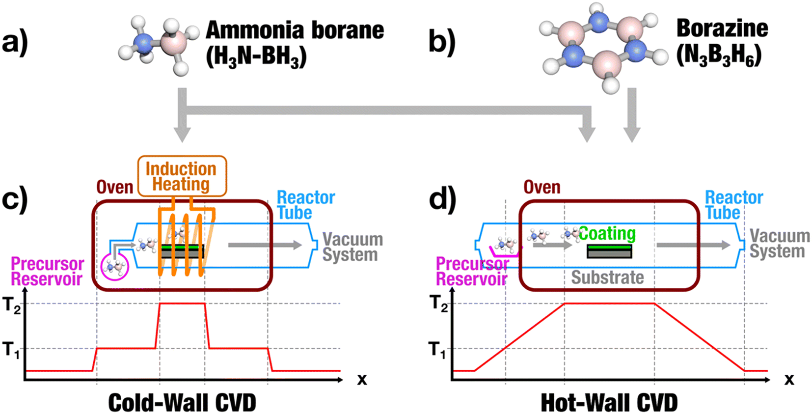 | ||
| Fig. 1 Schematic overview of different precursors: (a) ammonia borane (NH3BH3) and (b) borazine (N3B3H6) and deposition systems where these precursors were used. Hot-wall CVD (c) and inductively heated cold-wall CVD (d) with different temperature profiles during the deposition of hexagonal boron nitride (T1: sublimation temperature; T2: decomposition temperature). | ||
 | ||
| Fig. 2 Schematic representation of the thermal decomposition pathway of ammonia borane into amino borane, borazine and polymeric compounds, subsequently yielding hexagonal boron nitride under H2 elimination. | ||
Moreover, the decomposition of ammonia borane yields not only borazine but also polymeric structures like polyamine borane ([BH2NH2]x) and polyimino borane ([BHNH]x), which makes the detection of borazine in the gas phase somewhat unpredictable. Interestingly, some calculations propose that the formation of polyimino borane is energetically more favourable than that of borazine.40 Nonetheless, both byproducts contribute toward hBN formation. Borazine, also called “inorganic benzene” (B3N3H6), serves as another promising single source precursor for hBN growth due to pre-existing B–N bonds and possessing “B3N3” hexagons that can exert a templating effect in the synthesis of BN monolayer. However, its utilization is constrained by several factors such as high costs, toxicity, accessibility limitations that vary by country, and the requirement of specialized equipment for handling.
In most reports, catalytic substrates like copper,27,41 nickel,42 gold43 and platinum,44 have been employed. However, these substrates inevitably require transfer steps (bubble or etching transfer) for using hBN in electronic devices. The major hurdle in the use of hBN is related to lack of synthetic protocols enabling high-quality hBN on non-catalytic substrates, which would eliminate the need for additional transfer processes. Recent research demonstrates initial efforts toward direct deposition of hBN on sapphire and silicon substrates.45 Singhal and co-workers showed promising outcomes using ammonia borane in a low-pressure CVD set-up by direct deposition of hBN on silicon (100) and sapphire wafer.46 Despite achieving high-quality hBN compositions, the challenge persists in forming a continuous, ultra-thin film with a thickness in the range of a few nanometers or less as the thin film thickness can influence the functional properties.47
In this study, our objective was to conduct a comprehensive analysis of the influence of precursor chemistry, deposition parameters and substrate nature on the quality and phase purity of deposited hexagonal boron nitride. Initially, we examined the thermal deposition of ammonia borane on copper substrates in an atmospheric pressure set-up. Drawing from this experience, similar experiments were conducted on non-catalytic substrates, specifically silicon dioxide and sapphire. Lastly, we demonstrate successful deposition of few layer hBN achieved through the use of borazine in a low pressure hot-wall CVD reactor.
Results and discussion
Thin films of hexagonal boron nitride were grown in a hot-wall CVD set-up, as depicted in Fig. 1. To prevent potential clogging of exhaust pipelines due to precursor condensation, ammonia borane was placed inside the reactor tube. However, this arrangement was found to be challenging in controlling the thin film growth particularly due to limited control over the precursor flux during the deposition process.A series of experimental investigations was conducted to examine the correlation between substrate positioning and hBN coverage on the Cu substrate, akin to previously reported studies.28 A copper foil (length × width = 15 cm × 1 cm) was placed in a vertical tube furnace at atmospheric pressure and a homogeneous deposition temperature of 1050 °C throughout the whole substrate length (Fig. 3a). The quality and composition of the CVD deposits were analysed using vibrational spectroscopy (FT-IR) and microscopy (SEM). In contrast to previously reported observations,28 we found that positioning the substrate closer to the precursor inlet yielded better quality films rather than placing it towards the reactor outlet, which resulted in minimal coverage and lower quality hBN deposits. These variations may be possibly attributed to subtle differences in experimental set-ups and process parameters, such as varying tube diameters or gas flow rates.
 | ||
| Fig. 3 (a) Photograph of a coated copper substrate (length × width = 15 cm × 1 cm) with lateral changes of (b) spectroscopic (ATR-FT-IR) and (c) morphological (SEM) features at different sample positions (0.5 cm, 4.5 cm, 8.5 cm and 12.5 cm). The assignment of spectroscopic features follows the specific B–N–B out-of-plane (O; 792–811 cm−1), B–N in-plane (I; 1334–1382 cm−1) and N–H stretching (S; 1573 cm−1) modes. Signals inherent to the ATR-FT-IR measurement setup are marked with an asterisk (*). | ||
The typical hBN signals associated with B–N–B out-of-plane (805 cm−1) and B–N in-plane vibration (1350 cm−1)43 were found to be the most intense peaks in the IR spectra (Fig. 3b and ESI-Fig. 2†). No vibration signals associated with B–O (770 cm−1, 500 cm−1)32,33 or cBN (1068 cm−1) frequencies30,34 were detected. However, IR spectra recorded for substrate regions closer to the reactor outlet (sample position: 8.5 cm) displayed an additional vibration signal at 1573 cm−1, typically attributed to –NH2 groups, which might be due to limited lateral mobility and diffusion of precursor fragments and surface-bound species.35–37 This signal could possibly originate from undecomposed precursor groups or from N-terminated hBN flakes. Recent reports suggest the most stable forms of hBN involve N-termination, where open rings are terminated by NH2-groups.38 Measurements close to the precursor outlet (sample position: 12.5 cm) showed only B–N–B out-of-plane stretching vibrations with low intensity, as well as a peak at 2983 cm−1 (marked with *) specific to the ATR-FT-IR measurement set-up. Corresponding SEM images (Fig. 3c) show a declining substrate coverage, where the front part facing the precursor inlet (sample positions: 0.5 cm and 4.5 cm) exhibits a high coating homogeneity, while at the back part (sample positions: 8.5 cm and 12.5 cm) a poor coverage and sample quality is observed. The results obtained with optimal substrate position were chosen for further analysis and for optimizing the deposition parameter to achieve homogeneous film growth and uniform coverage of the substrates. Studies for optimizing the deposition temperature were conducted in the temperature range 800–1050 °C with steps of 25–50 °C, as the melting point of copper (1085 °C) defines the upper temperature limit and temperatures below 800 °C were already investigated to yield only nanocrystalline BN.48 Especially for ammonia borane, with its intrinsic disproportionation characteristics and decomposition reactions, which are affected by different solubilities of boron and nitrogen in copper, a precise control of the substrate temperature is essential for defined material deposition.40,49,50 ATR-FT-IR analysis confirmed the optimal deposition temperature of 1050 °C with highest quality of hBN and absence of noticeable NH2 vibrations (ESI-Fig. 1 and ESI-Table 1†).
Additional anaysis confirmed the formation of hBN at 1050 °C from ammonia borane in a hot wall reactor: Similar to graphene, the D- and G-bands vibration in the Raman spectra with the wavenumber 1336 cm−1 found to be overlapping with the prominent hBN signals at 1336 cm−1 and 1592 cm−1 (Fig. 4d and ESI-Fig. 5a†).51 The XPS spectra confirmed the presence of boron nitride with a small amount of oxygen (B![[thin space (1/6-em)]](https://www.rsc.org/images/entities/char_2009.gif) :N:O = 1.00:0.91:0.16) propably formed by the oxidation of unreacted precursor species (Fig. 4a–c). The morphology of the gained thin films (Fig. 4f) underly the further assumption of a heterogeneous CVD process and not dominated by reactions in the reaction zone of the gas phase similar to observations reported by Ismach et al.48 Only few particle-like structures were observed that could have formed in the gas phase due to predominant homogeneous nucleation instead of heterogeneous nucleation on the substrate surface.
:N:O = 1.00:0.91:0.16) propably formed by the oxidation of unreacted precursor species (Fig. 4a–c). The morphology of the gained thin films (Fig. 4f) underly the further assumption of a heterogeneous CVD process and not dominated by reactions in the reaction zone of the gas phase similar to observations reported by Ismach et al.48 Only few particle-like structures were observed that could have formed in the gas phase due to predominant homogeneous nucleation instead of heterogeneous nucleation on the substrate surface.
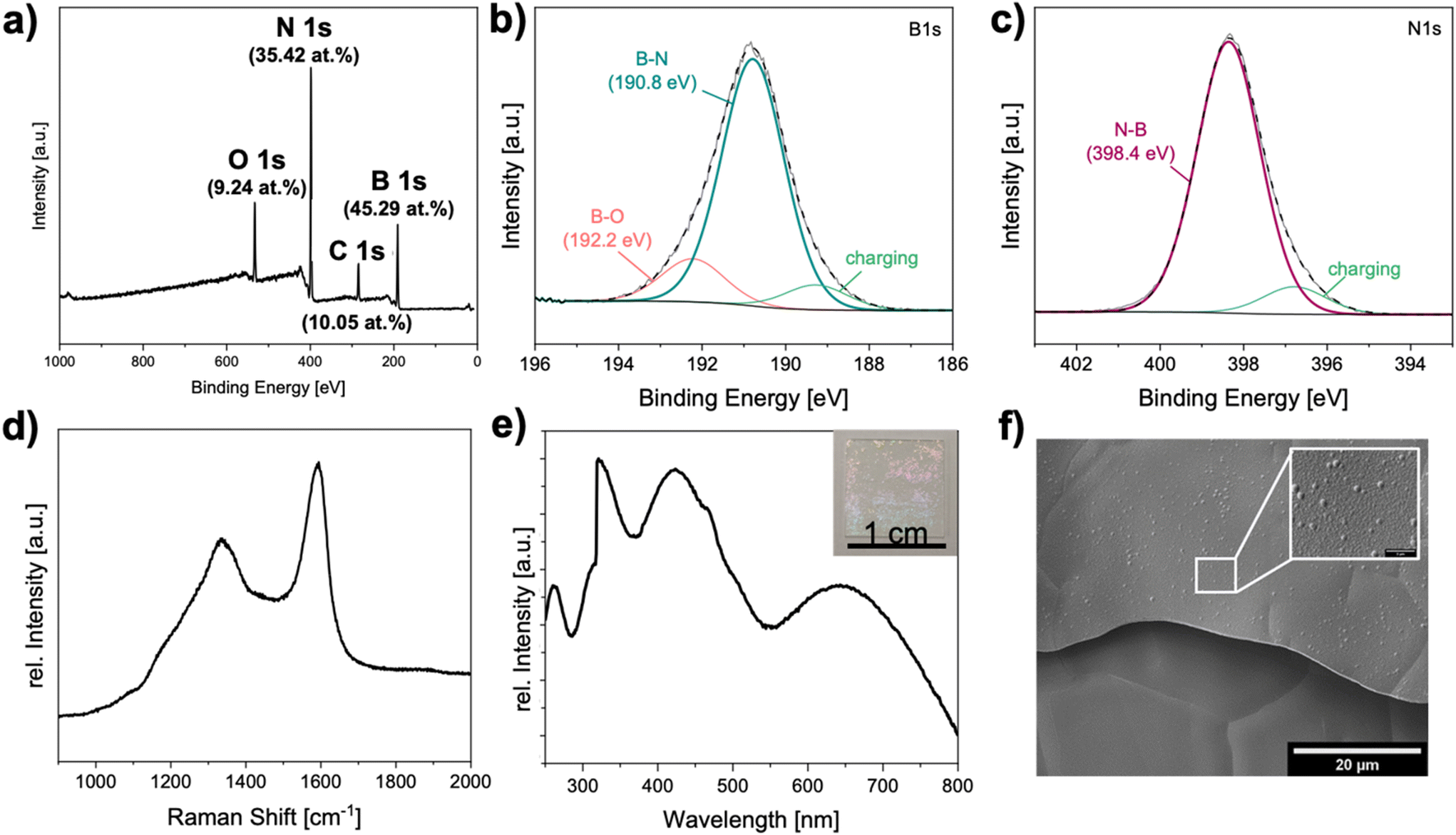 | ||
| Fig. 4 hBN deposition on copper foil using ammonia borane in a hot-wall CVD reactor: (a) Survey XPS spectra indicating a B:N-ratio of 1:0.9. High resolution XPS spectra of B 1s (b) and N 1s (c) core levels support the formation of BN with some surface oxidation present. Characteristic D- and G-band vibration visible in the Raman spectrum of as deposited thin films (d) and UV-Vis absorption (e) of transferred thin films (inset) on sapphire substrate. Homogeneous morphology of as deposited thin films visible in SEM (f). | ||
For AFM and UV-vis analyses of the CVD deposits, the samples were transferred on a sapphire substrate that also enabled determination of film thickness and analyzing the bending and stretching vibrations in the material. The surface of the transferred film was found to be smooth with an average roughness of 9 nm measured over an area of 10 μm2 wherease the overall thickness of the film was determined to be ca. 210 nm ( ESI-Fig. 7a, c†). The high average roughness compared to RMS values of around 3–4 nm.52,53 is possibly due to the buckling of the film during the cool down phase. The UV-vis spectra of films transferred on sapphire showed characteristic UV absorption (maximum at 250 nm) corresponding to the large band gap of hBN (∼6 eV) (Fig. 4e). Additional absorption peaks between 300–800 nm indicated non-uniform thickness and partial oxidation or contamination due to surface adsorbents, caused during the transfer process.
As-deposited thin-films were transferred onto TEM grids allowing both selected area electron diffraction (SAED) studies as well as high resolution imaging (Fig. 5). The (100) and (110) hBN lattice planes are clearly visible in the polycrystalline sample (Fig. 5a). Moreover, the bright spots indicate a preferred orientation and extended long range order, which is confirmed by high resolution image (Fig. 5b) also showing the same lattice planes in the FFT of two different regions of interest (ROI). The interplanar spacing was measured to be 3.6 Å, in accordance with literature values reported for hBN.31,40 The differences in the structural features in two selected regions (inset I and inset II) are possibly caused by the transfer process of the hBN thin film in conjunction with different film thicknesses of the hBN flakes, that overlap in some parts.
 | ||
| Fig. 5 TEM analysis of hBN films transferred on TEM grids (Quantifoil): (a) SAED diffraction pattern of hBN films with a radial profile (inset) to highlight the (100) and (110) lattice planes in a polycrystalline sample region with preferred orientation (bright spots). (b) Crystalline few layer hBN supported by FFT of selected ROIs clearly show the (100) and (110) lattice planes. | ||
In summary, layers of hBN with disordered topography and regional inhomogeneity in the film thickness were produced on a catalytic substrate (copper foil) by using ammonia borane in a hot-wall CVD reactor set-up.
In addition, hBN growth was evaluated using the same process conditions in a hot-wall CVD reactor enabling direct growth on non-catalytic substrates, with copper substrates acting as the reference. Single crystalline sapphire (α-Al2O3; c-plane (0001)) and silicon substrates with thermally grown SiO2 layer (SiO2@Si(100)) were chosen, due to their common usage in electronic device manufacturing. The IR-spectroscopic features of (I) N–H stretching (1575 cm−1), (II) B–N in-plane (1350 cm−1) and (III) B–N–B out-of-plane (805 cm−1), which are present on the Cu reference sample, are also visible – with significantly varying absolute intensities and intensity ratios – on the α-Al2O3 and SiO2@Si(100) substrates, respectively (Fig. 6a). Especially on the sapphire substrate (α-Al2O3) pronounced vibrational bands of the desired hBN thin films are obtained.
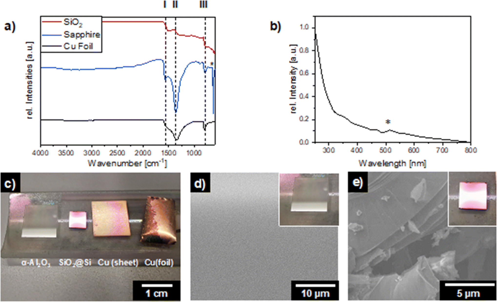 | ||
| Fig. 6 Hot-wall CVD of ammonia borane on sapphire (α-Al2O3), SiO2@Si(100), and copper (sheet, foil): (a) ATR-FT-IR spectra of the samples on different substrates; the asterisk marks a spectroscopic feature of the underlying sapphire substrate (b) UV-vis spectrum of as-deposited hBN on sapphire; the asterisk highlights an inherent spectrometer artifact caused by an internal lamp change. (c) Photograph of the as deposited hBN thin films on different substrates. SEM image with inset picture of the samples of hBN thin films on (d) α-Al2O3 and (e) SiO2@Si(100). | ||
The UV-vis spectra recorded on sapphire (Fig. 6b) supports this assumption exhibited an absorption in the UV region with a maximum below 250 nm which can be unambiguously attributed to the deposited material and corresponds to presumably hexagonal boron nitride. The accompanying SEM images of the films showed homogeneous morphology (Fig. 6d and e) with minimal roughness. Conversely, the SiO2 sample revealed multi-layered structures. This difference in morphology, in contrast to the deposition on copper foil, is presumably due to epitaxial growth on sapphire,54,55 whereas rougher surface in case of the silicon sample leads to non-uniform surface morphology.
In contrast to hBN growth on catalytic substrates (Cu), depositions on non-catalytic substrates such as sapphire highlight the need of higher deposition temperatures to facilitate sufficient mass transport and diffusion. So far, only few examples are known, where hBN films with sufficient film quality were obtained on non-catalytic substrates at the expense of significantly harsher process conditions (e.g. T > 1100 °C, low pressure, pre-treatment).46,56–58 The correlation of low-pressure process conditions with increased growth rates using ammonia borane on copper substrates was shown26 and might be transferred to future thin film growth of hBN on non-catalytic substrates. Moreover, different growth mechanisms for hBN formation on non-catalytic sapphire substrates were proposed with an initial B–O bond formation, which can however significantly affect the films characteristics.59
In contrast to hot-wall reactors with a continuous temperature profile (Fig. 1c), cold wall reactors offer a segmented temperature profile, which allows to separate evaporation and decomposition processes (Fig. 1d) and therefore provide a more controlled environment for the precursor decomposition. Moreover, the deposition process is carried out at low pressure (p = 10−4 mbar), thus effectively excluding intermolecular collisions of the precursor molecules, by extending the mean free path length from few nanometers (e.g. atmospheric pressure conditions in hot wall reactor) to several meters (low pressure cold wall reactor) and avoiding the necessity of reactive carrier gases (e.g. 5% H2 in Ar). The cold-wall reactor in its current configuration used in this study is limited to a maximum substrate temperature of Tmax = 950 °C.
The thin films resulting from the decomposition of ammonia borane in a low-pressure cold wall reactor exhibited strong N–H vibration bands due to residual amine groups alongside the B–N vibrations (Fig. 7a). The broad signal with peaks at 3227 and 3413 cm−1, indicated that under chosen experimental conditions, complete decomposition of ammonia borane was not achieved. Transferred films on sapphire (Fig. 7c and ESI-Fig. 7b, d†) showed a film thickness of 458 nm using AFM measurements, however given the limitations of attainable temperatures further depositions using this set-up were discontinued.
 | ||
| Fig. 7 Decomposition of ammonia borane in a low-pressure cold-wall CVD reactor on copper foil. (a) ATR-FT-IR spectrum of the films on copper with (b) associated stretching frequencies and peak intensities and (c) an AFM image of the thin film transferred on a sapphire substrate. | ||
In analogy to ammino borane, borazine is also a single-source precursor with hexagonally pre-organized B–N units that structurally resemble with the 2D structure of the desired hBN material. Interestingly, borazine is formed as an intermediate compound in the thermal decomposition of ammino borane (Fig. 2) to hBN, which exhibits a significantly higher reactivity for forming hBN compared to ammino borane and highlights the fact that initial precursor configuration is subject to bond-forming and bond-breaking phenomena that are intrinsic to the transformation of the molecular precursor into solid-state materials. Therefore, and due to the increased volatility of this compound, the precursor reservoir has to be maintained at −10 °C to ensure a constant precursor flow during the decompositions in a hot wall reactor. As confirmed by XPS analysis, the films have a 1:1 B–N ratio (Fig. 8a) and no oxidation of the films is observed (missing of B–O contributions in the high-resolution B 1s XPS spectrum; Fig. 8b), thus confirming that borazine leads to a more defined chemical composition in the deposited hBN films without any side products or secondary phases. Due to the low of films thickness, signals from the underlying copper substrate, as well as a relatively high oxygen content are visible in the survey spectrum (Fig. 8a). The Raman signal detected at 1369 cm−1 with a full width at half maximum (FWHM) of 17.3 cm−1 (Fig. 8d) is in accordance with reported characteristics of high-quality hBN films.11,60,61 The additional signals detected to the left and right of the hBN vibration are attributed to the underlying SiO2 substrate. AFM analysis (Fig. 8e and ESI-Fig. 8†) showed a step height of 1.7 nm which is equivalent to four-layer structured hBN as measurements of 2D films on SiO2 are often thicker than theoretical values of multiplying the interplanar distance under ambient conditions.11,62,63 The SEM micrographs of the as-deposited films confirm the uniform coverage of the copper substrate (Fig. 8f). The textured surface is characteristic for hBN monolayers as a result of substrate shrinkage during the cooling phase.64 This texturing effect is predominant in thicker films; however, it is no longer observable in the transferred films, apparently due to the relaxation of in-plane strain.
 | ||
| Fig. 8 hBN films grown on copper substrate in hot-wall CVD reactor using borazine as precursor: (a) the XPS survey spectrum suggests an equimolar B:N ratio together with high resolution spectra of (b) B 1s and (c) N 1s region. (d) Raman spectrum and (e) AFM image of transferred hBN on a SiO2 substrate with inset of the height profile. (f) SEM image with magnification of the as-grown hBN thin film. | ||
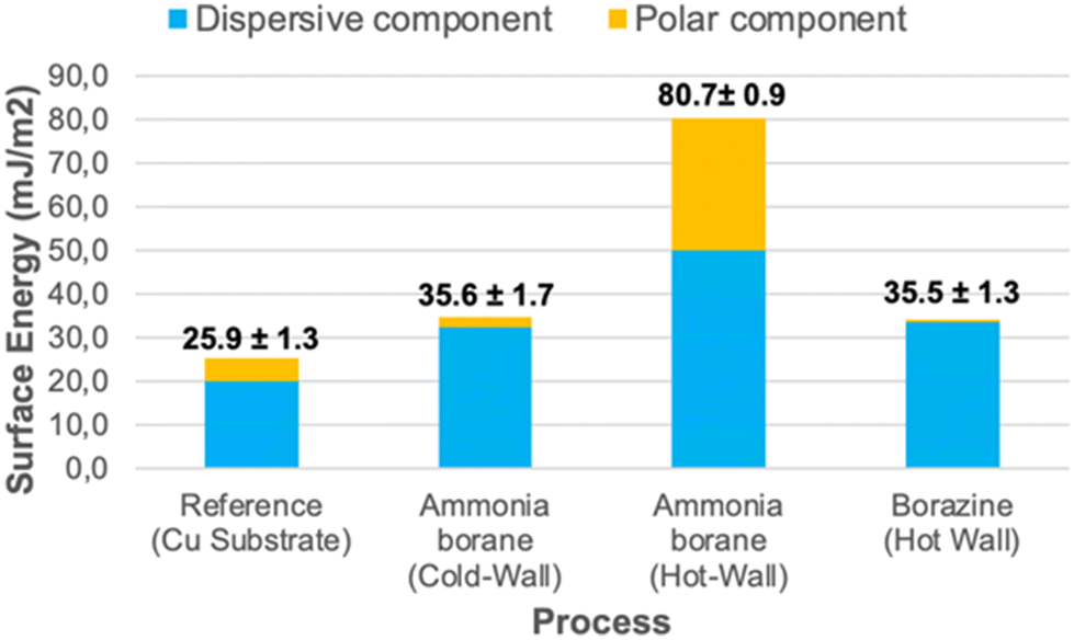
For application purposes, the wetting behaviour of 2D materials is an important criterion to fabricate electronic devices since the contact angle can be influenced by the morphology, thickness, and functional end groups of the thin film as well as defects and the underlying substrate.65 Moreover, it provides information whether a high or low energy surface is obtained. For this purpose, the contact angles of three different solvents (water, diiodomethane and ethylene glycol (EG)) were measured on the hBN films produced by hot-wall CVD using AB and borazine as well as by cold-wall CVD using AB and bare copper as reference, respectively (ESI-Fig. 9†). In a first approach all surfaces can be classified as low energy surfaces (Fig. 9),66 which show some deviation from the uncoated Cu reference substrate with a low surface energy of 25.4 ± 1.3 mJ m−2, supporting the existence of an oxidized copper surface.67 It is worth mentioning that, despite their different process conditions with ammonia borane deposited in a cold-wall reactor and borazine deposited in a hot-wall reactor, these surfaces yielded the lowest surface energy of similar value (35.6 ± 1.7 mJ m−2 and 35.5 ± 1.3 mJ m−2, respectively), with minimal contributions form polar components. On the other hand, ammonia borane deposited in a hot-wall reactor yields the highest surface energy (80.7 ± 0.9 mJ m−2) with the largest absolute (30.3 mJ m−2) and relative (37%) polar contributions of all hBN coatings, which is in line with the observed N–H moieties still present in the sample. Due to the fast spreading of the solvent on the hBN surface originating from the decomposition of ammonia borane in a hot-wall reactor low contact angle readings (≪10°) are afflicted with reasonable error. Nonetheless, the overall error of the surface energy can be estimated to 80.7 ± 0.9 mJ m−2.
 | ||
| Fig. 9 Surface energies as calculated by the Fowkes relationship of disperse and polar components through contact angle measurements of H2O and CH2I2 (data available in ESI-Table 2†). | ||
Conclusion
Gas phase depositions of hexagonal boron nitride were carried out using various chemical vapor deposition set-ups, including both hot and cold-wall configurations, and different precursor chemistries. The aim was to comparatively analyze the composition and structural quality of as-deposited boron nitride films. The collective analytical findings showed significant disparities in hBN quality depending contingent on the chosen CVD system and precursor composition. Although both ammonia borane and borazine proved to be suitable single-source precursors for producing phase-pure, high-quality hBN films, the comparison highlighted substantial differences depending on the chosen CVD configuration and parameters. Despite the advantages of ammonia borane in terms of ease of handling and low toxicity, the results obtained within the CVD set-up used in this work did not yield few or monolayer hBN of high quality and size. Nevertheless, these conditions can reproducibly produce insulating layers in the range of a few hundred nanometers. The most promising findings were achieved from decomposing borazine on a copper substrate in a hot-wall CVD system using an Ar/H2 mixture as the reactive carrier gas. In summary, this study presents the intricate interdependencies of precursor composition and CVD reactor configurations, as known in other coating systems68, in growing phase pure hBN thin films.Experimental section
Cleaning of the samples
The copper foils were sonicated in iso-propanol, acetone, and water for 10 min each and dried in air. Afterwards, they were treated with an etchant solution (Nickel etchant from Alfa Aesar, 044586.LV) for 2 min and washed with ethanol.Deposition of hBN using ammonia borane in hot-wall CVD reactor
The cleaned samples were placed in the middle of the reactor on a quartz piece. The deposition tube was flushed with an Ar/H2 mixture (95:5) for 45 min to remove the oxygen from the system. The reactor was than heated to the desired deposition temperature (Td = 1025 °C) with a heating rate of 10 °C min−1 and holding time of 1 h. Subsequently, ammonia borane (m = 100 mg, Sigma Aldrich, 95%) was gradually heated (70–140 °C) to transfer it in the gas phase (Table 1). After deposition, the substrate was annealed at the deposition temperature and with a continuous gas flow for 3 h.
| Process | Substrate | Precursor | T precursor [°C] | T substrate [°C] | p reactor [mbar] | Carrier gas |
|---|---|---|---|---|---|---|
| Hot-wall CVD | Cu, sapphire, SiO2@Si(100) | AB | 70–140 | 1025 | 1000 | H2/Ar |
| Cold-wall CVD | Cu | AB | 85 | 950 | 10−5 | — |
| Hot-wall CVD | Cu | Borazine | −10 | 1025 | 10−2 | H2/Ar |
Deposition of hBN using ammonia borane in Cold-wall CVD reactor
The clean substrates were placed on the substrate holder. Within a quartz glass tube and the set-up was evacuated to 10−5 mbar. Ammonia borane (50 mg, Sigma Aldrich, 95%) heated to Tp = 85 °C was introduced in the chamber and decomposed on the substrates heated to Td = 950 °C. The CVD process was run for a deposition time of 15 min (Table 1) and subsequently the substrates were cooled down.Deposition of hBN using borazine in Hot-wall CVD reactor
The cleaned copper foil was placed inside the reactor tube and the system was evacuated to 10−2 mbar for 20 min. Afterwards, the system was flushed with hydrogen (12 sccm) while maintaining the oven to 1025 °C for 1 h. After 20 min of annealing the substrate at the growth temperature, 2 min of film growth time was chosen using borazine (0.25 sccm, JSI Silicone) as precursor (Table 1).The precursor was maintained at −10 °C to prevent borazine polymerisation using a bath circulator from Jiotech with a mixture of ethyl glycol and DI water (6:4) as cooling medium.
Transfer of hBN thin films
For Raman analysis the as-deposited thin films were transferred to SiO2@Si(100) substrates. Firstly, the samples were spin coated with PMMA (MW ∼ 350 g mol−1, 1 M in chlorobenzene, 4000 rpm, 60 s). The layer was detached from the copper via bubble transfer using a 1 M NaOH solution. Following the transfer step, the hBN/PMMA film were washed with water and transferred on SiO2@Si(100) substrate. After drying the PMMA was removed by washing the samples several times with acetone.Characterization methods
The FT-IR spectra were recorded using a Spectrum 400 (PerkinElmer) in the range of 500–4000 cm−1 with four scans per sample, using a data interval of 1 nm and a scan speed of 266.75 nm min−1. The SEM measurements were performed on a 300 VP RISE field emission scanning microscope (FESEM) from Zeiss Sigma. The Raman spectra were recorded using a Lab Ram HR 800 spectrometer (Horiba Ltd) using a green line Ar+ ion laser (514.5 nm) in the range of 900–2000 cm−1. The XPS spectra were measured with an ESCA M-Probe spectrometer (Surface Science Instruments). A monochromatic Al Kα X-ray source (1486.6 eV, λ = 8.33 Å) was used and the spectra were recorded in the range of 0–1000 eV at ultra-high vacuum (10−9 mbar). The survey spectra were recorded using the following parameters: detector pass energy: 158.3 eV; step size: 0.5 eV; dwell time: 125 ms; data accumulation: seven scans per sample. High resolution spectra were recorded using the following parameters: detector pass energy: 55.2 eV; step size: 0.05 eV; dwell time: 175 ms; data accumulation: ten scans per sample (carbon) and 25 (other elements) were chosen, respectively. The data was evaluated using CASA XPS software suite (Casa Software Ltd). The UV-vis spectra were recorded using a LAMBDA 950 spectrometer (PerkinElmer). The samples were measured in the transmission mode compared to a reference consisting of the same substrate material. The AFM measurement of the sample thickness and surface structure of the BN layers were carried out on a XE-100 (Park System) atomic force microscope in a non-contact mode. High resolution transmission electron microscopy (HR-TEM) was carried out using a JEOL JEM 2200 FS equipped with UHR pole piece at 200 kV and an JEOL EDX detector. The thin films were transferred onto Quantifoil® Multi A10 copper grids (200 mesh). Data analysis was carried out using ImageJ software suite and dedicated macros. The contact angles were measured with the drop shape analysis system DSA 100 (KRÜSS GmbH). A defined amount (1 μL) of pure solvent (water, diiodomethane or ethylene glycol) is placed on the surface and the angle of the tangent between the baseline (substrate surface) and the solvent droplet is measured; each measurement is repeated on 3 independent positions and the resulting mean value is reported.Data availibility
The data supporting this article have been included as part of the ESI.†Conflicts of interest
The authors declare no competing conflict of interest.Acknowledgements
The authors kindly acknowledge the financial support offered by the German Science Foundation (DFG) for the project funding received in the frame of the International Research Training Group “Template-designed Organic Electronics” (IRTG 2591 – TIDE), the DFG research infrastructure grant (450610390 – Raman Imaging and Scanning Electron Microscope) and the financial and infrastructural support provided by the University of Cologne and Ulsan National Institute of Science and Technology. HSS and NB thank the support by Institute for Basic Science (IBS-R036-D). Further, we would like to thank Baris Öcal and PD Dr Selina Olthof from the University of Cologne for their support with XPS measurements. Mr Philipp Weitkamp and Prof. Klaus Meerholz from the University of Cologne are acknowledged for their help with the AFM analysis.References
- K. S. Novoselov, A. K. Geim, S. V. Morozov, D.-e. Jiang, Y. Zhang, S. V. Dubonos, I. V. Grigorieva and A. A. Firsov, Science, 2004, 306, 666–669 CrossRef CAS.
- A. K. Geim and K. S. Novoselov, Nat. Mater., 2007, 6, 183–191 CrossRef.
- S. Moon, J. Kim, J. Park, S. Im, J. Kim, I. Hwang and J. K. Kim, Adv. Mater., 2023, 35, 2204161 CrossRef PubMed.
- S. Vaidya, X. Gao, S. Dikshit, I. Aharonovich and T. Li, Adv. Phys.: X, 2023, 8, 2206049 Search PubMed.
- V. Brune, N. Raydan, A. Sutorius, F. Hartl, B. Purohit, S. Gahlot, P. Bargiela, L. Burel, M. Wilhelm, C. Hegemann, U. Atamtürk, S. Mathur and S. Mishra, Dalton Trans., 2021, 50, 17346–17360 RSC.
- V. Brune, C. Hegemann and S. Mathur, Inorg. Chem., 2019, 58, 9922–9934 CrossRef CAS.
- L. Wang, S. Yang, F. Zhou, Y. Gao, Y. Duo, R. Chen, J. Yang, J. Yan, J. Wang and J. Li, Small, 2023, 2306132 Search PubMed.
- S. Fukamachi, P. Solís-Fernández, K. Kawahara, D. Tanaka, T. Otake, Y.-C. Lin, K. Suenaga and H. Ago, Nat. Electron., 2023, 6, 126–136 CrossRef CAS.
- P. Ajayan, P. Kim and K. Banerjee, Phys. Today, 2016, 69, 9–38 CrossRef.
- R. Geick, C. Perry and G. Rupprecht, Phys. Rev., 1966, 146, 543 CrossRef CAS.
- T.-A. Chen, C.-P. Chuu, C.-C. Tseng, C.-K. Wen, H.-S. P. Wong, S. Pan, R. Li, T.-A. Chao, W.-C. Chueh and Y. Zhang, Nature, 2020, 579, 219–223 CrossRef CAS PubMed.
- L. Wang, X. Xu, L. Zhang, R. Qiao, M. Wu, Z. Wang, S. Zhang, J. Liang, Z. Zhang and Z. Zhang, Nature, 2019, 570, 91–95 CrossRef CAS PubMed.
- F. Zeng, R. Wang, W. Wei, Z. Feng, Q. Guo, Y. Ren, G. Cui, D. Zou, Z. Zhang and S. Liu, Nat. Commun., 2023, 14, 6421 CrossRef CAS PubMed.
- S. Roy, X. Zhang, A. B. Puthirath, A. Meiyazhagan, S. Bhattacharyya, M. M. Rahman, G. Babu, S. Susarla, S. K. Saju and M. K. Tran, Adv. Mater., 2021, 33, 2101589 CrossRef CAS.
- K. Kinoshita, R. Moriya, M. Onodera, Y. Wakafuji, S. Masubuchi, K. Watanabe, T. Taniguchi and T. Machida, npj 2D Mater. Appl., 2019, 3, 22 CrossRef.
- F. Yuan, W. Jiao, F. Yang, W. Liu, J. Liu, Z. Xu and R. Wang, J. Mater. Chem. C, 2017, 5, 6359–6368 RSC.
- D. Gonzalez Ortiz, C. Pochat-Bohatier, J. Cambedouzou, M. Bechelany and P. Miele, Nanomaterials, 2018, 8, 716 CrossRef PubMed.
- L. Pauling, J. Am. Chem. Soc., 1931, 53, 3225–3237 CrossRef.
- A. J. L. Catão and A. López-Castillo, J. Mol. Model., 2017, 23, 1–12 CrossRef.
- C.-L. Lo, M. Catalano, K. K. Smithe, L. Wang, S. Zhang, E. Pop, M. J. Kim and Z. Chen, npj 2D Mater. Appl., 2017, 1, 42 CrossRef.
- J. Wang, F. Ma, W. Liang and M. Sun, Mater. Today Phys., 2017, 2, 6–34 CrossRef.
- J. Eichler and C. Lesniak, J. Eur. Ceram. Soc., 2008, 28, 1105–1109 CrossRef CAS.
- J. Lee, A. V. Ravichandran, J. Mohan, L. Cheng, A. T. Lucero, H. Zhu, Z. Che, M. Catalano, M. J. Kim and R. M. Wallace, ACS Appl. Mater. Interfaces, 2020, 12, 36688–36694 CrossRef CAS.
- S. Le Gallet, G. Chollon, F. Rebillat, A. Guette, X. Bourrat, R. Naslain, M. Couzi and J.-L. Bruneel, J. Eur. Ceram. Soc., 2004, 24, 33–44 CrossRef CAS.
- X. Chen, C. Tan, X. Liu, K. Luan, Y. Guan, X. Liu, J. Zhao, L. Hou, Y. Gao and Z. Chen, J. Mater. Sci.: Mater. Electron., 2021, 32, 3713–3719 CrossRef CAS.
- W.-H. Lin, V. W. Brar, D. Jariwala, M. C. Sherrott, W.-S. Tseng, C.-I. Wu, N.-C. Yeh and H. A. Atwater, Chem. Mater., 2017, 29, 4700–4707 CrossRef CAS.
- Y. Uchida, T. Iwaizako, S. Mizuno, M. Tsuji and H. Ago, Phys. Chem. Chem. Phys., 2017, 19, 8230–8235 RSC.
- R. Y. Tay, X. Wang, S. H. Tsang, G. C. Loh, R. S. Singh, H. Li, G. Mallick and E. H. T. Teo, J. Mater. Chem. C, 2014, 2, 1650–1657 RSC.
- Y. Shi, C. Hamsen, X. Jia, K. K. Kim, A. Reina, M. Hofmann, A. L. Hsu, K. Zhang, H. Li, Z.-Y. Juang, M. S. Dresselhaus, L.-J. Li and J. Kong, Nano Lett., 2010, 10, 4143 Search PubMed.
- J. S. Lee, S. H. Choi, S. J. Yun, Y. I. Kim, S. Boandoh, J.-H. Park, B. G. Shin, H. Ko, S. H. Lee and Y.-M. Kim, Science, 2018, 362, 817–821 CrossRef CAS PubMed.
- D. Graf, J. Schläfer, S. Garbe, A. Klein and S. Mathur, Chem. Mater., 2017, 29, 5877–5885 CrossRef CAS.
- L. Jürgensen, D. Höll, M. Frank, T. Ludwig, D. Graf, A. K. Schmidt-Verma, A. Raauf, I. Gessner and S. Mathur, Dalton Trans., 2020, 49, 13317–13325 RSC.
- P. Tutacz, D. Stadler, T. Karimpour, T. s. Duchoň, S. Cramm, C. M. Schneider, T. Fischer, D. N. Mueller and S. Mathur, Chem. Mater., 2023, 35, 8050–8056 CrossRef CAS.
- U. Atamturk, E. Jung, T. Fischer and S. Mathur, Chem. Mater., 2022, 34, 7344–7356 CrossRef.
- S. Mathur, M. Veith, T. Ruegamer, E. Hemmer and H. Shen, Chem. Mater., 2004, 16, 1304–1312 CrossRef CAS.
- S. Frueh, R. Kellett, C. Mallery, T. Molter, W. S. Willis, C. King'ondu and S. L. Suib, Inorg. Chem., 2011, 50, 783–792 CrossRef CAS.
- P. Wang and X.-d. Kang, Dalton Trans., 2008, 5400–5413 RSC.
- E. Mayer, Inorg. Chem., 1972, 11, 866–869 CrossRef CAS.
- E. Mayer, Inorg. Chem., 1973, 12, 1954–1955 CrossRef CAS.
- C. R. Miranda and G. Ceder, J. Chem. Phys., 2007, 126, 184703-1–184703-11 CrossRef PubMed.
- M. Schwarz, A. Riss, M. Garnica, J. Ducke, P. S. Deimel, D. A. Duncan, P. K. Thakur, T.-L. Lee, A. P. Seitsonen and J. V. Barth, ACS nano, 2017, 11, 9151–9161 CrossRef CAS PubMed.
- H. Jeong, D. Y. Kim, J. Kim, S. Moon, N. Han, S. H. Lee, O. F. N. Okello, K. Song, S.-Y. Choi and J. K. Kim, Sci. Rep., 2019, 9, 1–8 CrossRef.
- Z. Zhang, X. Ji, J. Shi, X. Zhou, S. Zhang, Y. Hou, Y. Qi, Q. Fang, Q. Ji and Y. Zhang, ACS Nano, 2017, 11, 4328–4336 CrossRef CAS PubMed.
- T. H. Lee, K. Kim, G. Kim, H. J. Park, D. Scullion, L. Shaw, M.-G. Kim, X. Gu, W.-G. Bae and E. J. Santos, Chem. Mater., 2017, 29, 2341–2347 CrossRef CAS.
- A. Bansal, M. Hilse, B. Huet, K. Wang, A. Kozhakhmetov, J. H. Kim, S. Bachu, N. Alem, R. Collazo and J. A. Robinson, ACS Appl. Mater. Interfaces, 2021, 13, 54516–54526 CrossRef CAS PubMed.
- R. Singhal, E. Echeverria, D. N. McIlroy and R. N. Singh, Thin Solid Films, 2021, 733, 138812 CrossRef.
- T. Singh, T. Lehnen, T. Leuning, D. Sahu and S. Mathur, Appl. Surf. Sci., 2014, 289, 27–32 CrossRef.
- A. Ismach, H. Chou, D. A. Ferrer, Y. Wu, S. McDonnell, H. C. Floresca, A. Covacevich, C. Pope, R. Piner and M. J. Kim, ACS Nano, 2012, 6, 6378–6385 CrossRef PubMed.
- F. Baitalow, J. Baumann, G. Wolf, K. Jaenicke-Rößler and G. Leitner, Thermochim. Acta, 2002, 391, 159–168 CrossRef.
- A. Lozovoi and A. Paxton, Phys. Rev. B: Condens. Matter Mater. Phys., 2008, 77, 165413 CrossRef.
- L. M. Malard, M. A. Pimenta, G. Dresselhaus and M. S. Dresselhaus, Phys. Rep., 2009, 473, 51–87 CrossRef.
- J. C. Koepke, J. D. Wood, Y. Chen, S. W. Schmucker, X. Liu, N. N. Chang, L. Nienhaus, J. W. Do, E. A. Carrion and J. Hewaparakrama, Chem. Mater., 2016, 28, 4169–4179 CrossRef.
- J. Fernandes, T. Queirós, J. Rodrigues, S. S. Nemala, A. P. LaGrow, E. Placidi, P. Alpuim, J. B. Nieder and A. Capasso, FlatChem, 2022, 33, 100366 CrossRef.
- Q. Li, Q. Wu, J. Gao, T. Wei, J. Sun, H. Hong, Z. Dou, Z. Zhang, M. H. Rümmeli and P. Gao, Adv. Mater. Interfaces, 2018, 5, 1800662 CrossRef.
- A.-R. Jang, S. Hong, C. Hyun, S. I. Yoon, G. Kim, H. Y. Jeong, T. J. Shin, S. O. Park, K. Wong and S. K. Kwak, Nano Lett., 2016, 16, 3360–3366 CrossRef PubMed.
- R. Page, J. Casamento, Y. Cho, S. Rouvimov, H. G. Xing and D. Jena, Phys. Rev. Mater., 2019, 3, 064001 CrossRef.
- G. Wang, J. Meng, J. Chen, Y. Cheng, J. Huang, S. Zhang, Z. Yin, J. Jiang, J. Wu and X. Zhang, Cryst. Growth Des., 2022, 22, 7207–7214 CrossRef.
- M. Tokarczyk, A. K. Dąbrowska, G. Kowalski, R. Bożek, J. Iwański, J. Binder, R. Stępniewski and A. Wysmołek, 2D Mater., 2023, 10, 025010 CrossRef.
- R. Chen, Q. Li, Q. Zhang, J. Li, Z. Zhang, W. Fang, L. Wang, F. Yun, T. Wang and Y. Hao, Cryst. Growth Des., 2023, 23, 8783–8792 CrossRef.
- G. Kim, A.-R. Jang, H. Y. Jeong, Z. Lee, D. J. Kang and H. S. Shin, Nano Lett., 2013, 13, 1834–1839 CrossRef CAS.
- R. V. Gorbachev, I. Riaz, R. R. Nair, R. Jalil, L. Britnell, B. D. Belle, E. W. Hill, K. S. Novoselov, K. Watanabe and T. Taniguchi, Small, 2011, 7, 465–468 CrossRef CAS PubMed.
- D. Wickramaratne, L. Weston and C. G. Van de Walle, J. Phys. Chem. C, 2018, 122, 25524–25529 CrossRef CAS.
- M. Ishigami, J.-H. Chen, W. G. Cullen, M. S. Fuhrer and E. D. Williams, Nano Lett., 2007, 7, 1643–1648 CrossRef CAS PubMed.
- J. Lin, R. Y. Tay, H. Li, L. Jing, S. H. Tsang, H. Wang, M. Zhu, D. G. McCulloch and E. H. T. Teo, Nanoscale, 2018, 10, 16243–16251 RSC.
- D. Y. Kwok and A. W. Neumann, Adv. Colloid Interface Sci., 1999, 81, 167–249 CrossRef CAS.
- M. Annamalai, K. Gopinadhan, S. A. Han, S. Saha, H. J. Park, E. B. Cho, B. Kumar, A. Patra, S.-W. Kim and T. Venkatesan, Nanoscale, 2016, 8, 5764–5770 RSC.
- A. Ogwu and T. Darma, Sci. Rep., 2021, 11, 4276 CrossRef CAS.
- A. Mettenbörger, T. Singh, A. P. Singh, T. T. Järvi, M. Moseler, M. Valldor and S. Mathur, Int. J. Hydrogen Energy., 2014, 39(10), 4828–4835 CrossRef.
Footnote |
| † Electronic supplementary information (ESI) available. See DOI: https://doi.org/10.1039/d4nr02624a |
| This journal is © The Royal Society of Chemistry 2024 |