
 Open Access Article
 This Open Access Article is licensed under a Creative Commons Attribution-Non Commercial 3.0 Unported Licence
Field enhancement induced by surface defects in two-dimensional ReSe2 field emitters†
Filippo
Giubileo
 *a,
Enver
Faella
b,
Daniele
Capista
c,
Maurizio
Passacantando
b,
Ofelia
Durante
ad,
Arun
Kumar
d,
Aniello
Pelella
e,
Kimberly
Intonti
ad,
Loredana
Viscardi
ad,
Sebastiano
De Stefano
d,
Nadia
Martucciello
a,
Monica F.
Craciun
f,
Saverio
Russo
f and
Antonio
Di Bartolomeo
*ad
*a,
Enver
Faella
b,
Daniele
Capista
c,
Maurizio
Passacantando
b,
Ofelia
Durante
ad,
Arun
Kumar
d,
Aniello
Pelella
e,
Kimberly
Intonti
ad,
Loredana
Viscardi
ad,
Sebastiano
De Stefano
d,
Nadia
Martucciello
a,
Monica F.
Craciun
f,
Saverio
Russo
f and
Antonio
Di Bartolomeo
*ad
aCNR-SPIN Salerno, via Giovanni Paolo II n.132, 84084 Fisciano, Italy. E-mail: filippo.giubileo@spin.cnr.it
bDepartment of Physical and Chemical Science, University of L'Aquila, Via Vetoio, Coppito, 67100 L'Aquila, Italy
cIHP–Leibnitz Institut fuer innovative Mikroelektronik, 15236 Frankfurt (Oder), Germany
dDepartment of Physics “E.R. Caianiello”, University of Salerno, via Giovanni Paolo II n.132, 84084 Fisciano, Italy. E-mail: adibartolomeo@unisa.it
eDipartimento di Fisica, Università degli studi di Roma Tor Vergata, via della Ricerca Scientifica 1, 00133 Rome, Italy
fUniversity of Exeter, Stocker Road 6, Exeter EX4 4QL, Devon, UK
First published on 13th August 2024
Abstract
The field emission properties of rhenium diselenide (ReSe2) nanosheets on Si/SiO2 substrates, obtained through mechanical exfoliation, have been investigated. The n-type conduction was confirmed by using nano-manipulated tungsten probes inside a scanning electrode microscope to directly contact the ReSe2 flake in back-gated field effect transistor configuration, avoiding any lithographic process. By performing a finite element electrostatic simulation of the electric field, it is demonstrated that the use of a tungsten probe as anode, at a controlled distance from the ReSe2 emitter surface, allows the collection of emitted electrons from a reduced area that furtherly decreases by reducing the tip–sample distance, i.e. allowing a local characterization of the field emission properties. Experimentally, it is shown that the turn-on voltage can be linearly reduced by reducing the cathode–anode separation distance. By comparing the measured current–voltage characteristics with the numerical simulations, it is also shown that the effective field enhancement on the emitter surface is larger than expected because of surface defects. Finally, it is confirmed that ReSe2 nanosheets are suitable field emitters with high time stability and low current fluctuations.
1. Introduction
In recent years, the study of two-dimensional (2D) transition metal dichalcogenides (TMDs) has attracted growing interest in several fields, due to the extraordinary physical, chemical, and electronic properties that can be exploited in a great number of applications.1 For instance, field effect transistors (FETs) based on TMDs are characterized by dangling bonds free surfaces that favour channel thickness reduction down to a monolayer.2 TMDs also show exceptional quantum efficiency and high photoluminescence, allowing the development of high-performance photodetectors.3–5 Among TMDs, particular attention is recently triggered by rhenium dichalcogenides, (chemical formula ReX2, with X = Se, S) for their distorted structure with a triclinic symmetry (1T phase) that originates anisotropic electrical and optical properties.6,7 The strong in-plane anisotropy is due to the one-dimensional chain arrangement of Re4 parallelograms, and it causes a weak coupling between layers so that also in the bulk arrangement they electronically and vibrationally behave as decoupled monolayers. Moreover, differently from hexagonal semiconducting TMDs, ReX2 does not show a transition from indirect to direct band gap upon reducing the layer number to one, making it a promising material for various technological advancements in electronics and beyond. For example, monolayer ReSe2 has an indirect bandgap of 1.34 eV, which remains indirect in the bulk crystal albeit reducing its value to 0.98 eV.8 However, the nature of the fundamental optical band gap in this material remains under debate: theoretical and experimental band gaps of ReSe2 are given in the exhaustive review by P. Satheesh et al.6 Top-gated ReSe2 FETs have shown a high on/off current ratio, and carrier mobility that increases for reducing thickness.9 Several studies have been focused on the exploitation of ReSe2 in optoelectronic applications.10–13 On the other hand, no investigations have been reported about the possible use of ReSe2 nanosheets as cold cathode field emitters. The motivation for this kind of characterization is mostly related to the great potential of field emission (FE) sources for application in vacuum electronic devices.14–16 Indeed, compared to thermionic emission, FE has great advantages, such as low-power consumption, high emission current density, and narrow electron energy distribution. Consequently, FE devices can be fruitfully exploited in vacuum electronics for developing X-ray sources,17 high-frequency electronics,18 FE vertical transistors,19,20 FE displays,21 and power switching devices.22 Indeed, in FE devices no heating is required to extract the electrons, but rather a sufficiently large external electric field, that makes the vacuum barrier lower and thinner, favouring the electron emission via quantum tunnelling process. Moreover, small curvatures are extremely relevant because they contribute to locally enhance electric field on the surface of the emitter. Consequently, several nanostructures are the subject of investigation to characterize their field emission properties. The prototype of nanostructured field emitters have been, since their discovery, the carbon nanotubes (CNTs).23–25 These have been the focus of a plethora of studies, to include metallic and semiconductor films26–28 and nanotubes,29–31 as single tubes,32–34 aligned tubes35–37 and networks.38–43 As well, in recent years attention has been focused also on 2D materials, starting from graphene,44–47 and then continuing with various TMDs, either as isolated flakes48–50 or as ensemble of vertically grown flakes, including MoS2![[thin space (1/6-em)]](https://www.rsc.org/images/entities/char_2009.gif) 40 and graphene nanoflowers.51
40 and graphene nanoflowers.51
In this paper, a detailed investigation of the field emission properties of multilayer ReSe2 laying on Si/SiO2 substrates is reported. The electrical properties of the flake are characterized using two retractable nano-manipulated tungsten probe tips in direct electrical contact with the surface of the flake, inside a scanning electron microscope (SEM). The silicon substrate acts as a back-gate electrode allowing a three-terminal configuration as field effect transistor and evidencing a clear modulation of the current flowing in the ReSe2 channel between the two tips working as drain and source. By retracting the drain tip electrode at controlled distance from the flake, we can use it as an anode to collect electrons emitted by the flake in a field emission configuration. The main performance parameters of the emitter, such as turn-on voltage and field enhancement factor have been estimated. By performing detailed simulations of the electric field, it is shown that field enhancement α ≈ 30 induced by surface defects is necessary to allow the experimentally observed FE current intensity. Finally, current stability is confirmed by reporting current fluctuations as small as 5%.
2. Experiment
A commercially available crystal of ReSe2 in bulk form (HQ Graphene, Netherlands) was used to obtain ReSe2 nanosheets by standard scotch tape method, in which the tape is pressed onto the bulk ReSe2 crystal and then pulled off very carefully. The ReSe2 layers become thinner after each pull and nanosheets are available on the tape after numerous repetitions. The ReSe2 nanosheets are then transferred on clean silicon substrate covered with a thermally grown 290 nm thick SiO2 layer, by simply pressing the tape on the substrate surface and then carefully removing it.The ReSe2 crystal structure is shown in Fig. 1a. A selected multilayer flake, for which a SEM image is reported in Fig. 1b, has been identified and characterized by energy dispersive X-ray (EDX) and atomic force microscopy (AFM).
 | ||
| Fig. 1 (a) Schematic of ReSe2 crystal structure, showing views of monolayer along the three axis (a-, b-, and c-). (b) SEM image of the ReSe2 nanosheet under investigation. (c) Energy dispersive spectra measured in the two locations marked on the SEM image. (d) Energy dispersive map for the ReSe2 nanosheet. (e) AFM image of the ReSe2 nanosheet and (f) measurement of three different height profiles as marked on the image. | ||
EDX spectra have been measured on both the flake (position P2 marked on the SEM image) and the substrate (position P1). Despite the overlap with the signal coming from the substrate, the two peaks related to Re and Se (at 1.86 keV and 1.40 keV, respectively) are clearly visible in the spectrum measured on the flake (Fig. 1c). Fig. 1d shows the elemental mapping of Re, Se, Si, O collected by EDX over the whole area imaged by the SEM, which confirms a uniform spatial distribution of Se and Re elements across the ReSe2 flake, while no significant impurities are evidenced. Finally, a topographic measurement of the flake by AFM (Fig. 1e and f) confirms the multilayer nature of the studied flake consisting of terraces with thicknesses in the range from 3–60 nm. We notice that the field emission characterization reported in section 3.2 has been performed in the large flat surface in close proximity of the position P2 as indicated in Fig. 1b.
The experiment was performed at a base pressure of 10−6 Torr inside a SEM (Zeiss LEO 1530), equipped with two piezo-driven nanomanipulators (Kleindiek MM3A) for precise positioning of metallic (tungsten) probe-tips with step resolution of about 5 nm. The metallic tips, which function as in situ electrodes, are connected to a Keithley 4200 SCS (semiconductor parameter analyzer) enabling electrical measurements with bias voltage ranging from 0 up to 120 V and current measurements with resolution <0.1 pA. A schematic of the experimental setup is drawn in Fig. 2a.
 | ||
| Fig. 2 (a) Schematic of the experimental setup with sample placed under vacuum in SEM chamber, with two metallic tips working as nano-manipulated electrodes (source and drain); Si substrate is connected to gate bias supplier. (b) Transfer characteristic Id–Vgs measured soon after the approach of the metallic tips on the flake surface at fixed drain bias Vds = 3 V. (c) Comparison of the I–V curves measured before (black curve) and after (blue curve) the electrical stress. (d) Transfer characteristic Id–Vgs measured after the electrical stress. | ||
3. Results and discussion
3.1. Transistor characterization
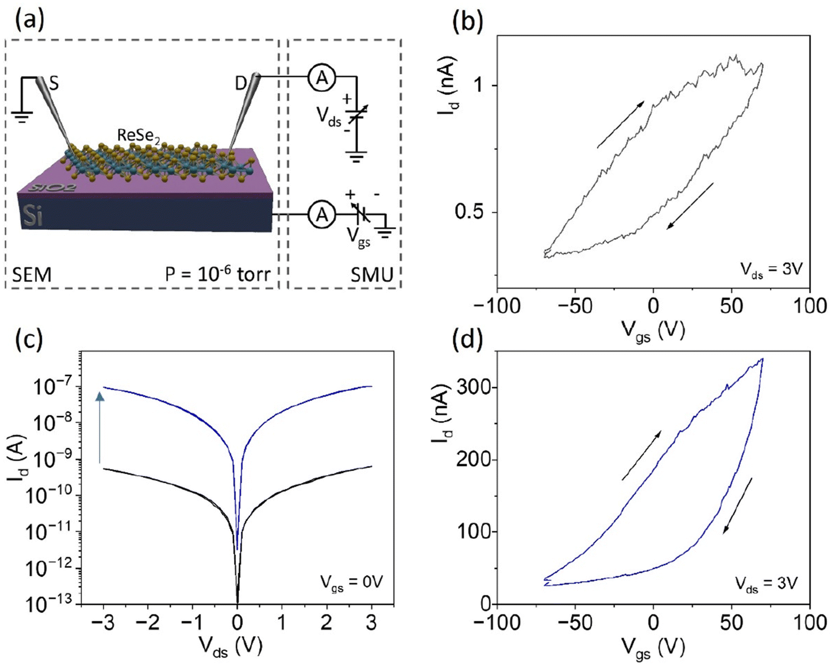
As the first characterization step, measurements of the transport properties of the ReSe2 flake have been performed. The flake lays on commercial Si/SiO2 substrate with a 290 nm thick oxide layer. Consequently, the Si substrate can be operated as a back gate in a three-terminal FET configuration, in which ReSe2 is the conductive channel. To maintain the intrinsic properties of the flake, the electron beam lithography and the lift-off process typically used for evaporating metal electrodes has been bypassed. Instead, electrical contacts on the flake have been established through a direct approach using nano-manipulated tungsten probes within the scanning electron microscope. The tips of these probes were employed as the source and drain electrodes of the device. This approach ensures minimal alteration of the intrinsic properties of the flake throughout the fabrication process.52 Indeed, techniques based on electron beams (or ion beams) can significantly modify the electronic properties of atomically thin materials by causing structural damages and/or point defects and/or dislocations, all of which can behave as charge traps and modify the device's performance. For instance, it has been reported that modifications of the electronic properties of 2D materials can be induced by electron and/or ion irradiation.53–56As standard characterization, both the transfer characteristic, i.e. the channel current Id as function of the gate voltage Vgs for fixed drain voltage Vds, and the output characteristic, in which the Id is measured as a function of Vds for fixed Vgs have been measured. In Fig. 2b, we report the Id–Vgs curve measured soon after the contact of the tips with the ReSe2 is realized, showing a current modulation in the range from 300 pA to 1 nA, while sweeping the gate voltage in a loop in the range ± 70 V. The limited current intensity and the fluctuations suggest the existence of unstable electrical contacts characterized by high resistance. We notice that by applying a negative gate bias the channel current decreases, typical of a n-type device. Moreover, larger gate bias was avoided to prevent oxide/device failure. We also estimated the field effect carrier mobility as  , where CSiO2 = 1.15 × 10⁻⁸ F cm−2 is the capacitance per unit area of the SiO2 layer with a thickness of 290 nm,
  is the FET transconductance (corresponding to the slope of the transfer characteristic), and L and W are the transistor channel length and width, respectively (for which is assumed as L the distance between the tips ∼20 μm and their diameter ∼200 nm as W). The obtained mobility is low with respect to usually reported values (0.1–100 cm2 V−1 s−1) for ReSe2 based FETs on Si/SiO2 substrates.57,58 In most cases, multilayer ReSe2 based FETs in two-probe configurations have shown electron-doped like response in the range 1–10 cm2 V−1 s−1. The relatively low value extracted from Fig. 2b can be originated by a high contact resistance as well as by impurities/defects at the ReSe2/SiO2 interface and adsorbates on the channel surface.
The device was then measured after an electrical stress (i.e., prolonged drain biasing at 10 V), which is suitable for improving the metal–ReSe2 coupling (thus reducing the contact resistance) and favouring the desorption of surface contaminants.59 In Fig. 2c, the output curves Id–Vds (at fixed Vgs = 0 V) measured before and after the electrical stress that stabilizes the device, significantly increasing the conductivity, are compared.60,61 The improved stability is also confirmed in the transfer characteristic successively measured and reported in Fig. 2d. The increased conductivity and stability of the transistor resulted in much larger field-effect mobility that has been estimated as μ = (19.2 ± 0.7) cm2 V−1 s−1 (the absolute values here reported could be slightly overestimated due to the assumption on the channel width). The FET performance is stabilized and improved by the electrical stress procedure. We notice that the current modulation is improved, and it is of about one order of magnitude. This value agrees with the values already reported for ReSe2 based FETs working at low pressure,10 while larger modulation is reported when working in air (ambient pressure).10,12,57,62,63
3.2. Field emission characterization
The field emission characterization of the ReSe2 can be easily performed by keeping one probe tip (the cathode) in contact with the flake, while retracting the second tip (the anode) at controlled distance from the sample surface. The piezo-driven nanomanipulator allows a fine tuning of the cathode–anode separation distance d. The main advantage of using a tip-shaped anode is related to the possibility to get local information about the field emission properties.Indeed, the use of a tip anode has a double effect: first, the FE is a tunnelling phenomenon and thus the probability of electron emission from regions of the sample far from the tip exponentially decreases with the increasing distance; second, the electric field at the sample surface decreases for increasing distance from the tip axis. Consequently, when performing FE experiments with the tip anode, the effective sample area contributing to the emission is limited and it depends on the separation distance.
In the following a simulation analysis of the FE configuration exploiting the tip anode is reported. More specifically, the COMSOL MULTIPHYSICS software was used to perform a finite element electrostatic simulation of the electric field generated by an applied potential difference between tip and sample in the FE setup. A 2D model including a planar surface separated by the metallic tip by a vacuum gap is considered. ReSe2 emitting surface is simply treated as an infinitely thin perfect 2D metal. By solving the Laplace equation by finite element method, the software allows the estimation of the electric field at any point of the designed model. The tip-anode was modelled with curvature radius of 100 nm, while the cathode–anode separation distance was varied in the range 200–700 nm. The distribution of the electric field calculated for a cathode–anode separation distance d = 200 nm is reported in Fig. 3a. The simulation allows the easy extraction of the field intensity on the emitter surface as a function of the distance r from the projection of the tip axis. As expected, the electric field profile has a radial symmetry and the intensity depends on the separation d, as shown in Fig. 3b.
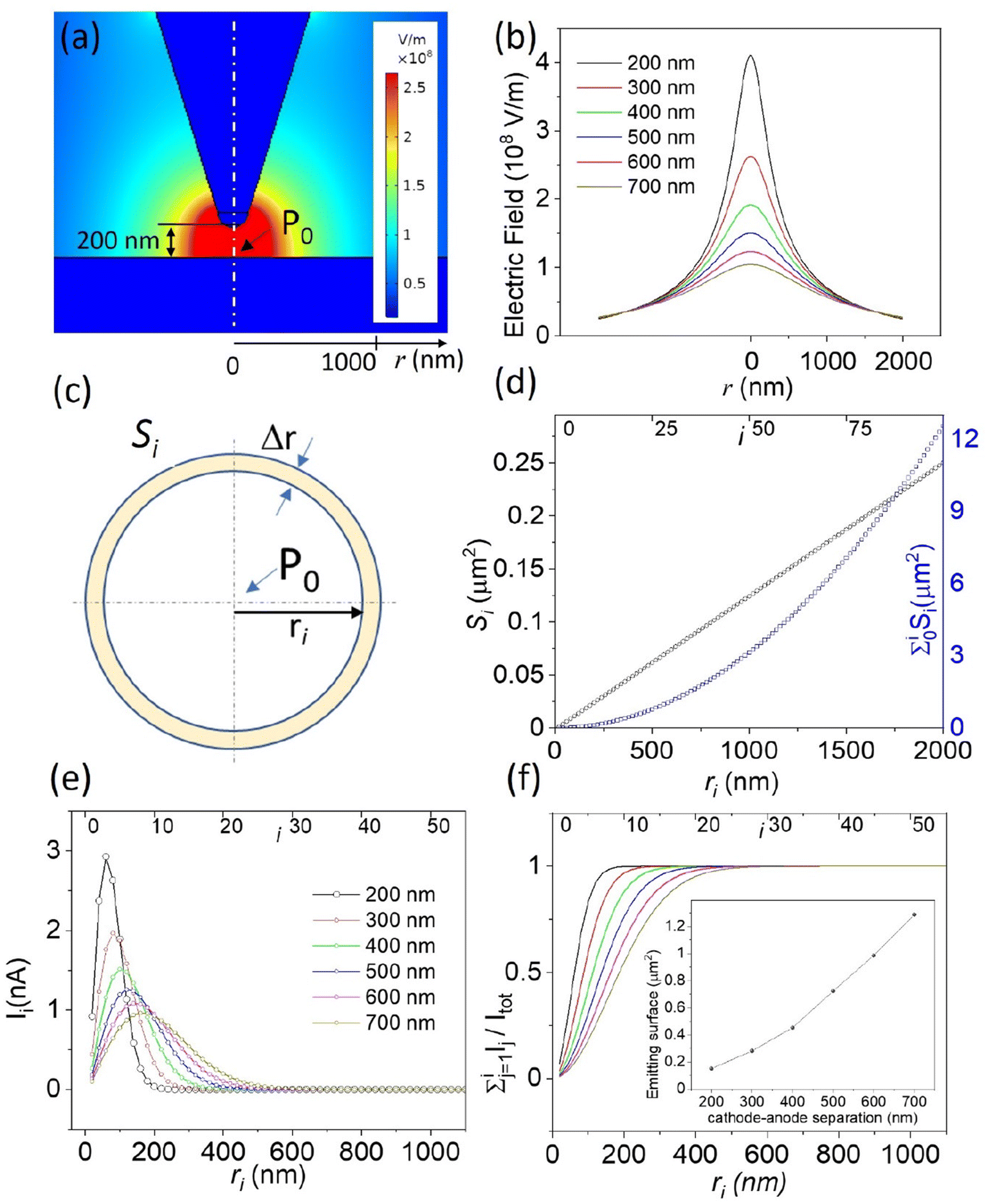 | ||
Fig. 3 (a) Simulated FE setup with tip-anode (curvature radius of 100 nm) separated by d = 200 nm from a planar emitting surface. Colour scale refers to calculated electric field intensity. (b) Electric field profile on the emitting surface as a function of r, i.e., the distance from the tip axis. (c) Schematic of the generic area element Si used to calculate the FE current in eqn (1). (d) Dependence of Si on ri. (e) FE current emitted from each annulus Si for different cathode–anode separation distances. (f) Total current emitted from a circle of radius ri, normalized to  . In the inset, effective emitting area as a function of the cathode–anode separation distance. . In the inset, effective emitting area as a function of the cathode–anode separation distance. | ||
The field emission current was calculated according to the Fowler–Nordheim (FN) theory64 in which the current can be expressed as:
 | (1) |
 , is compared to the total current
  . For the maximum separation d = 700 nm all the FE current comes from a circular region with radius Rd=700 nm ≈ 600 nm, the other contributions at larger distances being negligible. For the minimum investigated separation d = 200 nm the effective emitting area is reduced to about 0.12 μm2. These results confirm that the use of FE setup equipped with tip-anode is a powerful technique to perform local characterization of the FE properties.
From an experimental point of view, the FE measurements have been performed by positioning the anode at a controlled distance from the ReSe2 flake in a range between 200 nm and 700 nm (schematic of the setup is shown in Fig. 4a). A positive bias sweep (typically from 0 to +100 V) is applied to the anode, while measuring the current flowing in the circuit. The current–voltage (I–V) characteristic measured at the larger distance d = 700 nm is reported (on linear scale) in Fig. 4b, showing an exponential growth of the current that reaches about 40 nA at 100 V. To better identify the turn-on voltage Von (here defined as the voltage necessary to obtain a current of 1 pA) the I–V curve is also reported on logarithmic scale (in the inset of Fig. 4b). For bias up to 70 V, no FE current is collected at the anode, and the plot just shows the floor noise of our setup at the level between 10−14 A and 10−13 A. For larger bias, V > 70 V, the electron emission is activated (Von = 70 V) and the current exponentially increases. In Fig. 4c, a schematic of the energy band diagram of the FE system is shown: left panel depicts the band diagram of ReSe2 and tungsten (W) referred to the vacuum level at thermal equilibrium; right panel shows the case in which high positive bias is applied to the tungsten tip causing an important band bending at the vacuum/ReSe2 interface. The accumulation of electrons provides an increase of charges available for the emission through the vacuum barrier.
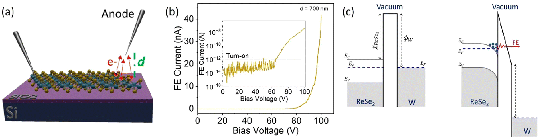 | ||
| Fig. 4 (a) Schematic of the FE device in which the tungsten tip working as anode is retracted at controlled distance from the sample (emitter) surface. (b) FE I–V characteristic (on linear scale) measured with the anode at a distance d = 700 nm from the emitter surface. In the inset the I–V curve is shown on logarithmic scale. (c) Schematic energy band diagram of the FE device (ReSe2/vacuum/W-tip): left panel shows the situation without applied bias. For V = 0 V, all bands remain flat, and the semiconductor and its majority and minority carriers are in thermal equilibrium. Right panel shows the diagram for positive bias on the W-tip. The positive bias applied to the W-tip (right scheme) induces band bending at the ReSe2/vacuum interface favouring the accumulation of the majority carriers (electrons) near the interface. | ||
The measurements have been repeated by reducing the anode–cathode separation distance d from 700 nm to 200 nm (by steps of 100 nm). I–V curves are reported in Fig. 5a, where it is observed a reduction of the turn-on voltage for reduced spacing between the anode and the emitting surface (Fig. 5b). Experimental I–V characteristics are compared to theoretical curves obtained as numerical fit to eqn (1), in which we considered a local electric field Elocali = αEi locally enhanced by a factor α to take into account real surface effects not considered in the simplified model where the emitting surface is schematized as a perfectly flat surface. α is a fitting parameter (dimensionless) that represents the field enhancement necessary to obtain the real current intensity, otherwise too low in case of considering uniquely the electric field in presence of a perfect flat emitting surface. The real surface is characterized by defects, such as ripples, contaminations, vacancies, and edges, that significantly modify the surface geometry causing significant enhancement of the local electric field in presence of very small curvature radius. A larger local field corresponds to a much higher emitted current, according to eqn (1). It is worth noticing that considering the effective emitting area for a cathode–anode separation distance of 200 nm, the emitted current density, at anode bias of +60 V, is about 7.2 × 10⁵ A m−2.
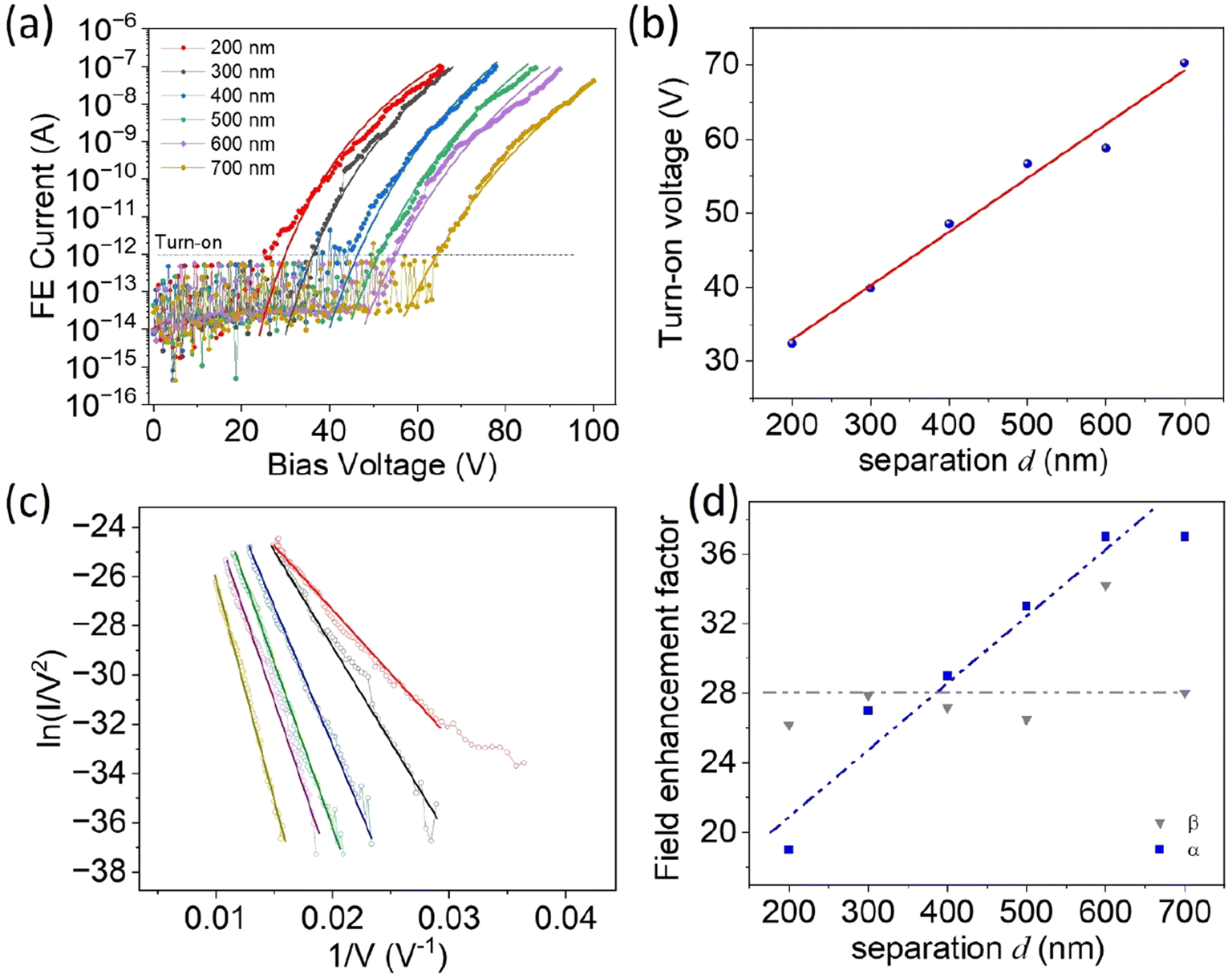 | ||
| Fig. 5 (a) FE current–voltage curves measured for cathode–anode separation distance varying between 200 nm and 700 nm. Experimental data (dotted curves) are compared to numerical fittings to eqn (1) (solid curves). (b) Turn-on voltage as a function of the separation distance. Solid line is a linear fit of the data. (c) Fowler–Nordheim plots (dotted curves) corresponding to the I–V curves reported in the plot (a). Solid lines are the linear fits of the data, whose slope is used to extract the standard field enhancement factor β. (d) The field enhancement factor β extracted by the first-approximation approach to use the standard simplified FN formula is compared to the enhancement factor α due to the surface defects (dashed lines are guides for eyes). | ||
The FN model was developed for the simplest case in which the emitter is a flat surface, and electrons are emitted at zero kelvin through a triangular potential barrier. However, despite its simplicity, the model is widely used as standard first-approximation reference method to analyze and identify the FE phenomenon also in more complex systems including several kinds of nanostructures. According to the model, a linear dependence of ln(I/V2) versus 1/V is expected (the so-called FN-plot), as shown in Fig. 5c. The linearity of the FN plots is a confirmation of the FE nature of the measured current. Usually, the slope m of the FN plots is used to extract the field enhancement factor β = d·B·ϕ3/2/m, which represents an average parameter. We can then compare it with the more precise α parameter extracted by fitting the experimental I–V curves to eqn (1). The α and β parameters are compared in Fig. 5d: the effective surface induced enhancement is dependent on the cathode separation distance, with α increasing for increasing separation.
We notice that that for large vacuum gate, the electron emission current–voltage characteristics can transit into space-charge-limited current (SCLC)65 at the high-bias regime. SCLC is not observed in our experimental data reported in Fig. 5a and c. Indeed, FN plots have better linear fit at larger vacuum gap. This seems to be in agreement with theoretical prediction66 for which SCLC is absent in 2D materials.
For the sake of completeness we mention that in recent years several theoretical studies have focused on the necessity of developing more complex models better suited to describe the phenomenon of vertical electron emission from the surface of 2D materials, by taking into account the reduced dimensionality, and several further effects, such as nonparabolic energy dispersion, finite-temperature, space-charge limited current, etc.67,68
Finally, the FE current stability is investigated. The anode tip is positioned at d = 200 nm from the emitting surface, and an I–V curve (Fig. 6a) has been preliminary recorded to confirm the FE configuration. Then, we applied a fixed bias (Vbias = 70 V) between tip and sample, while monitoring the FE current for a period of several minutes. The result of the stability test is reported in Fig. 6b, where a FE current relatively stable as a function of time is observed. The statistical analysis of the measured current values, shown in Fig. 6c, exhibits a Gaussian distribution around the average value of 0.25 μA with a standard deviation of 0.01 μA.
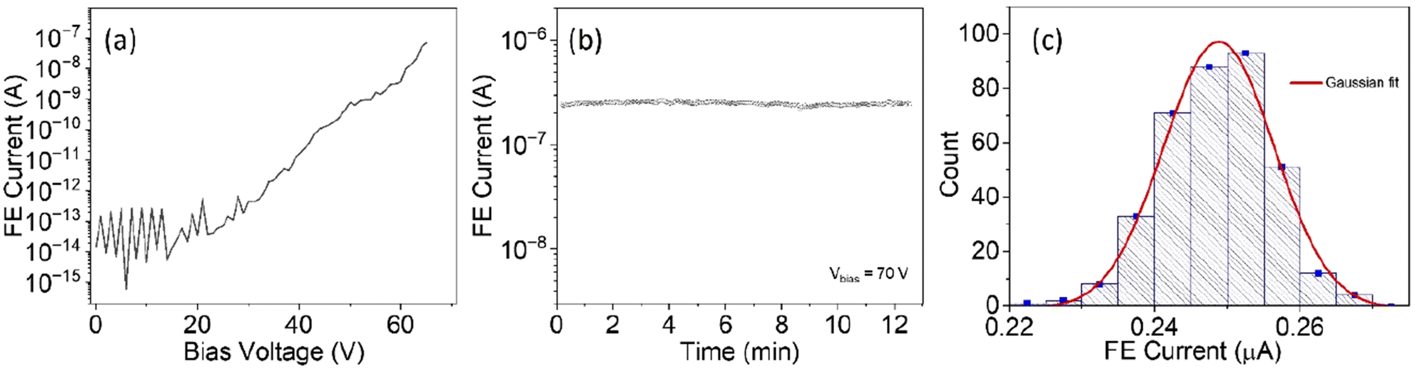 | ||
| Fig. 6 (a) FE current measured as function of voltage for d = 200 nm; (b) FE current stability measured at d = 200 nm and fixed voltage bias of 70 V between anode and cathode; (c) statistical analysis of FE current: histogram of measured FE current values and gaussian fit (red line). | ||
To complete our analysis, we report in Table 1, the comparison of the field emission properties of several 2D materials and other nanostructures, including well established field emitters such as carbon nanotubes, all characterized with the same local technique, exploiting a tip shaped anode, with cathode–anode separation distance below 2 μm.
| Material | Cathode–anode separation (nm) | Turn-on field or voltage | Field enhancement factor | Time stability | Ref. |
|---|---|---|---|---|---|
| Graphene monolayer | 100–600 nm | 600 V μm−1 | — | 100 min | 45 |
| Graphene flowers | 400–700 nm | 70–78 V μm−1 | 16–32 | 150 s | 51 |
| Graphene/InP nanocrystals | 570–1000 nm | 90–115 V μm−1 | 30–45 | — | 69 |
| GeSn nanocrystals | 500–700 nm | 65 V μm−1 | 105–130 | 8 h | 70 |
| MW-CNT film | 400–2000 nm | 100 V | 50 | 8 h | 43 |
| Aligned CNTs | 250–550 nm | 140 V μm−1 | 30 | 12 h | 42 |
| WS2 nanotubes | 400 nm | 100 V μm−1 | 65 | — | 71 |
| GaAs nanowires | 150–900 nm | 150 V μm−1 | 20–80 | 60 min | 33 |
| WSe2 monolayer | 400 nm | 80–140 V μm−1 | 60 | 25 min | 19 |
| MoS2 bilayers | 10–200 nm | 20–70 V | 4–16 | — | 72 |
| MoS2 few-layers | 250–2000 nm | 20 V μm−1 | 50–500 | 8 h | 73 |
| MoS2 nanosheets | 200–400 nm | 40–60 V | 16–17 | 25 min | 20 |
| ReSe2 nanosheets | 200–700 nm | 30–70 V | 19–38 | 12 min | This work |
4. Conclusions
Exfoliated ReSe2 nanosheets have been studied as two-dimensional field emitters by exploiting a nano-manipulated tip-shaped anode to collect electrons from limited areas, with dimensions as small as 0.1 μm2 for a cathode–anode separation distance of 200 nm. Simulation of the electric field distribution demonstrates that field enhancement induced by surface defects is necessary to obtain the experimentally observed current intensity. Additionally, it is shown that the turn-on voltage linearly depends on the separation distance. Finally, we showcase high stability of the FE current, with fluctuations less than 5%. Our results pave the way for the exploitation of ReSe2 nanosheets, as well as other two-dimensional materials, for realizing a new generation of miniaturized X-ray tubes and flexible displays.Author contributions
Filippo Giubileo: Conceptualization; data curation; formal analysis; investigation; methodology; supervision; writing – original draft; writing – review & editing. Enver Faella: Data curation; formal analysis; investigation; validation; visualization. Daniele Capista: Data curation; investigation; software; visualization. Maurizio Passacantando: Conceptualization; funding acquisition; investigation; methodology; validation. Ofelia Durante: Data curation; software; visualization. Arun Kumar: Data curation; software; visualization. Aniello Pelella: Data curation; software; visualization. Kimberly Intonti: Data curation; software; visualization. Loredana Viscardi: Data curation; software; visualization. Sebastiano De Stefano: Data curation; software; visualization. Nadia Martucciello: Data curation; software; visualization. Monica F. Craciun: Formal analysis; funding acquisition; investigation; resources; writing – review & editing. Saverio Russo: Formal analysis; funding acquisition; investigation; resources; writing – review & editing. Antonio Di Bartolomeo: Conceptualization; funding acquisition; resources; supervision; validation; writing – review & editing. All authors discussed the experimental procedures and results.Data availability
The data supporting this article have been included as part of the ESI.†Conflicts of interest
The authors declare that they have no known competing financial interests or personal relationships that could have appeared to influence the work reported in this paper.Acknowledgements
M. F. C. and S. R. acknowledge financial support from The Leverhulme Trust (grants “Graded excitonics” and “Giant Permittivity”), from “TERASSE” EU-H2020-MSCA-RISE (grant n. 823878), EPSRC (EP/Y021339/1, EP/V048163/1, EP/S019855/1, EP/M001024/1, EP/V052306/1, and EP/M002438/1). For the purpose of open access, the author has applied a ‘Creative Commons Attribution (CC BY) licence to any Author Accepted Manuscript version arising from this submission. E. F. acknowledges Progetti di Ateneo finanziati per l'Avvio alla Ricerca 2024 – Università degli Studi dell'Aquila.References
- S. Manzeli, D. Ovchinnikov, D. Pasquier, O. V. Yazyev and A. Kis, Nat. Rev. Mater., 2017, 2, 17033 CrossRef CAS.
- M. Chhowalla, D. Jena and H. Zhang, Nat. Rev. Mater., 2016, 1, 16052 CrossRef CAS.
- J. An, X. Zhao, Y. Zhang, M. Liu, J. Yuan, X. Sun, Z. Zhang, B. Wang, S. Li and D. Li, Adv. Funct. Mater., 2022, 32, 2110119 CrossRef CAS.
- A. Di Bartolomeo, A. Kumar, O. Durante, A. Sessa, E. Faella, L. Viscardi, K. Intonti, F. Giubileo, N. Martucciello, P. Romano, S. Sleziona and M. Schleberger, Mater. Today Nano, 2023, 24, 100382 CrossRef CAS.
- Z. Wu, W. Jie, Z. Yang and J. Hao, Mater. Today Nano, 2020, 12, 100092 CrossRef.
- P. P. Satheesh, H.-S. Jang, B. Pandit, S. Chandramohan and K. Heo, Adv. Funct. Mater., 2023, 33, 2212167 CrossRef CAS.
- T. U. Tran, D. A. Nguyen, N. T. Duong, D. Y. Park, D. H. Nguyen, P. H. Nguyen, C. Park, J. Lee, B. W. Ahn, H. Im, S. C. Lim and M. S. Jeong, Appl. Mater. Today, 2022, 26, 101285 CrossRef.
- D. Wolverson, S. Crampin, A. S. Kazemi, A. Ilie and S. J. Bending, ACS Nano, 2014, 8, 11154–11164 CrossRef CAS PubMed.
- S. Yang, S. Tongay, Y. Li, Q. Yue, J.-B. Xia, S.-S. Li, J. Li and S.-H. Wei, Nanoscale, 2014, 6, 7226–7231 RSC.
- E. Faella, K. Intonti, L. Viscardi, F. Giubileo, A. Kumar, H. T. Lam, K. Anastasiou, M. F. Craciun, S. Russo and A. Di Bartolomeo, Nanomaterials, 2022, 12, 1886 CrossRef CAS PubMed.
- Y. Tong, F. Kong, L. Zhang, X. Hou, Z. Zha, Z. Hao, J. Dai, C. Sun, J. Song, H. Huang, C. Ji, L. Pan and D. Li, Appl. Phys. Lett., 2024, 124, 083102 CrossRef CAS.
- K. Intonti, E. Faella, L. Viscardi, A. Kumar, O. Durante, F. Giubileo, M. Passacantando, H. T. Lam, K. Anastasiou, M. F. Craciun, S. Russo and A. Di Bartolomeo, Adv. Electron. Mater., 2023, 9, 2300066 CrossRef CAS.
- P. D. Patil, M. Wasala, R. Alkhaldi, L. Weber, K. K. Kovi, B. Chakrabarti, J. A. Nash, D. Rhodes, D. Rosenmann, R. Divan, A. V. Sumant, L. Balicas, N. R. Pradhan and S. Talapatra, J. Mater. Chem. C, 2021, 9, 12168–12176 RSC.
- X. Fang, Y. Bando, U. K. Gautam, C. Ye and D. Golberg, J. Mater. Chem., 2008, 18, 509–522 RSC.
- F. Giubileo, A. Di Bartolomeo, L. Iemmo, G. Luongo and F. Urban, Appl. Sci., 2018, 8, 526 CrossRef.
- S. Zhao, H. Ding, X. Li, H. Cao and Y. Zhu, Mater. Sci. Semicond. Process., 2023, 167, 107804 CrossRef CAS.
- Z. Lin, P. Xie, R. Zhan, D. Chen, J. She, S. Deng, N. Xu and J. Chen, ACS Appl. Nano Mater., 2019, 2, 5206–5213 CrossRef CAS.
- L. B. De Rose, W. M. Jones and A. Scherer, Appl. Phys. Lett., 2023, 123, 013505 CrossRef CAS.
- A. Di Bartolomeo, F. Urban, M. Passacantando, N. McEvoy, L. Peters, L. Iemmo, G. Luongo, F. Romeo and F. Giubileo, Nanoscale, 2019, 11, 1538–1548 RSC.
- A. Pelella, A. Grillo, F. Urban, F. Giubileo, M. Passacantando, E. Pollmann, S. Sleziona, M. Schleberger and A. Di Bartolomeo, Adv. Electron. Mater., 2021, 7, 2000838 CrossRef CAS.
- P. Liu, Y. Wei, K. Liu, L. Liu, K. Jiang and S. Fan, Nano Lett., 2012, 12, 2391–2396 CrossRef CAS PubMed.
- N. Shimoi and K. Tohji, Appl. Mater. Today, 2022, 26, 101284 CrossRef.
- F. Giubileo, A. D. Bartolomeo, A. Scarfato, L. Iemmo, F. Bobba, M. Passacantando, S. Santucci and A. M. Cucolo, Carbon, 2009, 47, 1074–1080 CrossRef CAS.
- J.-M. Bonard, K. A. Dean, B. F. Coll and C. Klinke, Phys. Rev. Lett., 2002, 89(19), 197602 CrossRef PubMed.
- M. Passacantando, F. Bussolotti, S. Santucci, A. Di Bartolomeo, F. Giubileo, L. Iemmo and A. M. Cucolo, Nanotechnology, 2008, 19, 395701 CrossRef CAS PubMed.
- R.-Z. Wang, W. Zhao and H. Yan, Sci. Rep., 2017, 7, 43625 CrossRef.
- A. Grillo, J. Barrat, Z. Galazka, M. Passacantando, F. Giubileo, L. Iemmo, G. Luongo, F. Urban, C. Dubourdieu and A. Di Bartolomeo, Appl. Phys. Lett., 2019, 114, 193101 CrossRef.
- Y. Shen, Y. Yang, Y. Gong, S. Yu, H. Hei and H. Gong, J. Mater. Res. Technol., 2022, 18, 4314–4328 CrossRef CAS.
- Y. Li, Z. Zhang, G. Zhang, L. Zhao, S. Deng, N. Xu and J. Chen, ACS Appl. Mater. Interfaces, 2017, 9, 3911–3921 CrossRef CAS PubMed.
- F. Giubileo, M. Passacantando, F. Urban, A. Grillo, L. Iemmo, A. Pelella, C. Goosney, R. LaPierre and A. Di Bartolomeo, Adv. Electron. Mater., 2020, 6, 2000402 CrossRef CAS.
- J. Yuan, H. Li, Q. Wang, X. Zhang, S. Cheng, H. Yu, X. Zhu and Y. Xie, Mater. Lett., 2014, 118, 43–46 CrossRef CAS.
- Z. Lin, H. Chen, J. She, S. Deng and J. Chen, Vacuum, 2022, 195, 110660 CrossRef CAS.
- F. Giubileo, A. Di Bartolomeo, L. Iemmo, G. Luongo, M. Passacantando, E. Koivusalo, T. Hakkarainen and M. Guina, Nanomaterials, 2017, 7, 275 CrossRef PubMed.
- W. Zhu, W. Qian, R. Liu, W. Huang, H. Luo and C. Dong, Vacuum, 2022, 199, 110933 CrossRef CAS.
- K. K. Yadav, Sunaina, M. Sreekanth, S. Ghosh, A. K. Ganguli and M. Jha, Appl. Surf. Sci., 2020, 526, 146652 CrossRef CAS.
- F. Giubileo, A. Di Bartolomeo, Y. Zhong, S. Zhao and M. Passacantando, Nanotechnology, 2020, 31, 475702 CrossRef CAS PubMed.
- G. Kumar, H. Gupta, S. Ghosh and P. Srivastava, Phys. E, 2022, 135, 114946 CrossRef CAS.
- F. Giubileo, E. Faella, A. Pelella, A. Kumar, D. Capista, M. Passacantando, S. S. Kim and A. Di Bartolomeo, Adv. Electron. Mater., 2022, 2200237 CrossRef CAS.
- J. Yan, Y. Huang, Z. Cao and Y. An, Vacuum, 2023, 208, 111725 CrossRef CAS.
- F. Giubileo, A. Grillo, M. Passacantando, F. Urban, L. Iemmo, G. Luongo, A. Pelella, M. Loveridge, L. Lozzi and A. Di Bartolomeo, Nanomaterials, 2019, 9, 717 CrossRef CAS PubMed.
- P. Tyagi, C. Ramesh, A. Sharma, S. Husale, S. S. Kushvaha and M. Senthil Kumar, Mater. Sci. Semicond. Process., 2019, 97, 80–84 CrossRef CAS.
- F. Giubileo, L. Iemmo, G. Luongo, N. Martucciello, M. Raimondo, L. Guadagno, M. Passacantando, K. Lafdi and A. Di Bartolomeo, J. Mater. Sci., 2017, 52, 6459–6468 CrossRef CAS.
- F. Giubileo, A. Di Bartolomeo, M. Sarno, C. Altavilla, S. Santandrea, P. Ciambelli and A. M. Cucolo, Carbon, 2012, 50, 163–169 CrossRef CAS.
- Q. Ji, B. Wang, Y. Zheng, F. Zeng and B. Lu, Diamond Relat. Mater., 2022, 124, 108940 CrossRef CAS.
- S. Santandrea, F. Giubileo, V. Grossi, S. Santucci, M. Passacantando, T. Schroeder, G. Lupina and A. Di Bartolomeo, Appl. Phys. Lett., 2011, 98, 163109 CrossRef.
- Y. Li, X. Li, L. Luo, Y. Meng, Z. Qin, J. He and R. Wang, Surf. Interfaces, 2023, 40, 103036 CrossRef CAS.
- A. Di Bartolomeo, F. Giubileo, L. Iemmo, F. Romeo, S. Russo, S. Unal, M. Passacantando, V. Grossi and A. M. Cucolo, Appl. Phys. Lett., 2016, 109, 023510 CrossRef.
- R. Ławrowski, L. Pirker, K. Kaneko, H. Kokubo, M. Bachmann, T. Ikuno, M. Remskar and R. Schreiner, J. Vac. Sci. Technol., B: Nanotechnol. Microelectron.: Mater., Process., Meas., Phenom., 2020, 38, 032801 Search PubMed.
- A. Di Bartolomeo, A. Pelella, F. Urban, A. Grillo, L. Iemmo, M. Passacantando, X. Liu and F. Giubileo, Adv. Electron. Mater., 2020, 6, 2000094 CrossRef CAS.
- T.-H. Yang, K.-C. Chiu, Y.-W. Harn, H.-Y. Chen, R.-F. Cai, J.-J. Shyue, S.-C. Lo, J.-M. Wu and Y.-H. Lee, Adv. Funct. Mater., 2018, 28, 1706113 CrossRef.
- F. Giubileo, D. Capista, E. Faella, A. Pelella, W. Y. Kim, P. Benassi, M. Passacantando and A. Di Bartolomeo, Adv. Electron. Mater., 2023, 9, 2200690 CrossRef CAS.
- L. Iemmo, F. Urban, F. Giubileo, M. Passacantando and A. Di Bartolomeo, Nanomaterials, 2020, 10, 106 CrossRef CAS PubMed.
- M. S. Choi, M. Lee, T. D. Ngo, J. Hone and W. J. Yoo, Adv. Electron. Mater., 2021, 7, 2100449 CrossRef CAS.
- A. Pelella, O. Kharsah, A. Grillo, F. Urban, M. Passacantando, F. Giubileo, L. Iemmo, S. Sleziona, E. Pollmann, L. Madauß, M. Schleberger and A. Di Bartolomeo, ACS Appl. Mater. Interfaces, 2020, 12, 40532–40540 CrossRef CAS PubMed.
- X. Wu, X. Luo, H. Cheng, R. Yang and X. Chen, Nanoscale, 2023, 15, 8925–8947 RSC.
- A. Di Bartolomeo, F. Urban, A. Pelella, A. Grillo, M. Passacantando, X. Liu and F. Giubileo, Nanotechnology, 2020, 31, 375204 CrossRef CAS PubMed.
- S. Song, G. Zhang, J. Qiao, B. Chen, M. Shen, X. Yuan, M. G. Somekh and F. Feng, Phys. B, 2023, 663, 415000 CrossRef CAS.
- N. R. Pradhan, C. Garcia, B. Isenberg, D. Rhodes, S. Feng, S. Memaran, Y. Xin, A. McCreary, A. R. H. Walker, A. Raeliarijaona, H. Terrones, M. Terrones, S. McGill and L. Balicas, Sci. Rep., 2018, 8, 12745 CrossRef PubMed.
- J. Moser, A. Barreiro and A. Bachtold, Appl. Phys. Lett., 2007, 91, 163513 CrossRef.
- S. B. Mitta, M. S. Choi, A. Nipane, F. Ali, C. Kim, J. T. Teherani, J. Hone and W. J. Yoo, 2D Mater., 2020, 8, 012002 CrossRef.
- D. S. Schulman, A. J. Arnold and S. Das, Chem. Soc. Rev., 2018, 47, 3037–3058 RSC.
- J. Kim, K. Heo, D. Kang, C. Shin, S. Lee, H. Yu and J. Park, Adv. Sci., 2019, 6, 1901255 CrossRef CAS PubMed.
- J. Y. Park, H.-E. Joe, H. S. Yoon, S. Yoo, T. Kim, K. Kang, B.-K. Min and S. C. Jun, ACS Appl. Mater. Interfaces, 2017, 9, 26325–26332 CrossRef CAS PubMed.
- R. H. Fowler and L. Nordheim, Proc. R. Soc. London, Ser. A, 1928, 119, 173–181 CAS.
- P. Zhang, Y. S. Ang, A. L. Garner, Á. Valfells, J. W. Luginsland and L. K. Ang, J. Appl. Phys., 2021, 129, 100902 CrossRef CAS.
- C. Chua, C. Y. Kee, Y. S. Ang and L. K. Ang, Phys. Rev. Appl., 2021, 16, 064025 CrossRef CAS.
- W. J. Chan, C. Chua, Y. S. Ang and L. K. Ang, IEEE Trans. Plasma Sci., 2023, 51, 1656–1670 CAS.
- L. K. Ang, Y. S. Ang and C. H. Lee, Phys. Plasmas, 2023, 30, 033103 CrossRef CAS.
- L. Iemmo, A. Di Bartolomeo, F. Giubileo, G. Luongo, M. Passacantando, G. Niu, F. Hatami, O. Skibitzki and T. Schroeder, Nanotechnology, 2017, 28, 495705 CrossRef CAS PubMed.
- A. Di Bartolomeo, M. Passacantando, G. Niu, V. Schlykow, G. Lupina, F. Giubileo and T. Schroeder, Nanotechnology, 2016, 27, 485707 CrossRef PubMed.
- A. Grillo, M. Passacantando, A. Zak, A. Pelella and A. Di Bartolomeo, Small, 2020, 16, 2002880 CrossRef CAS PubMed.
- F. Urban, M. Passacantando, F. Giubileo, L. Iemmo and A. Di Bartolomeo, Nanomaterials, 2018, 8, 151 CrossRef PubMed.
- F. Giubileo, L. Iemmo, M. Passacantando, F. Urban, G. Luongo, L. Sun, G. Amato, E. Enrico and A. Di Bartolomeo, J. Phys. Chem. C, 2019, 123, 1454–1461 CrossRef CAS.
Footnote |
| † Electronic supplementary information (ESI) available. See DOI: https://doi.org/10.1039/d4nr02109f |
| This journal is © The Royal Society of Chemistry 2024 |