
 Open Access Article
 This Open Access Article is licensed under a
 Creative Commons Attribution 3.0 Unported Licence
Functionalization of three-dimensional epitaxial graphene with metal nanoparticles†
Emanuele
Pompei
 *a,
Ylea
Vlamidis
ab,
Letizia
Ferbel
a,
Valentina
Zannier
a,
Silvia
Rubini
c,
Daniel Arenas
Esteban
de,
Sara
Bals
de,
Carmela
Marinelli
b,
Georg
Pfusterschmied
f,
Markus
Leitgeb
f,
Ulrich
Schmid
f,
Stefan
Heun
a and
Stefano
Veronesi
*a
*a,
Ylea
Vlamidis
ab,
Letizia
Ferbel
a,
Valentina
Zannier
a,
Silvia
Rubini
c,
Daniel Arenas
Esteban
de,
Sara
Bals
de,
Carmela
Marinelli
b,
Georg
Pfusterschmied
f,
Markus
Leitgeb
f,
Ulrich
Schmid
f,
Stefan
Heun
a and
Stefano
Veronesi
*a
aNEST, Istituto Nanoscience-CNR and Scuola Normale Superiore, Piazza S. Silvestro 12, 56127, Pisa, Italy. E-mail: emanuele.pompei@sns.it; stefano.veronesi@nano.cnr.it
bDepartment of Physical Science, Earth, and Environment, University of Siena, Via Roma 56, 53100, Siena, Italy
cIstituto Officina Dei Materiali IOM - CNR, Laboratorio TASC, Area Science Park, S.S.14, Trieste, I-34149, Italy
dEMAT, University of Antwerp, Groenenborgerlaan 171, B-2020, Antwerp, Belgium
eNanolab Centre of Excellence, Groenenborgerlaan 171, B-2020, Antwerp, Belgium
fInstitute of Sensor and Actuator Systems, TU Wien, 1040, Vienna, Austria
First published on 25th July 2024
Abstract
We demonstrate the first successful functionalization of epitaxial three-dimensional graphene with metal nanoparticles. The functionalization is obtained by immersing three-dimensional graphene in a nanoparticle colloidal solution. This method is versatile and demonstrated here for gold and palladium, but can be extended to other types of nanoparticles. We have measured the nanoparticle density on the top surface and in the porous layer volume by scanning electron microscopy and scanning transmission electron microscopy. The samples exhibit a wide coverage of nanoparticles with minimal clustering. We demonstrate that high-quality graphene promotes the functionalization, leading to higher nanoparticle density both on the surface and in the pores. X-ray photoelectron spectroscopy shows the absence of contamination after the functionalization process. Moreover, it confirms the thermal stability of the Au- and Pd-functionalized three-dimensional graphene up to 530 °C. Our approach opens new avenues for utilizing three-dimensional graphene as a versatile platform for catalytic applications, sensors, and energy storage and conversion.
Introduction
Inorganic porous materials have found a large variety of applications in the last few decades. Their main feature is their large surface area-to-volume ratio. Therefore, they have been employed in the fields of catalysis,1 fluid absorption,2 plasmonic wave resonators,3 sensors,4,5 energy storage and conversion,6,7 and drug delivery.8Among all porous materials, those based on carbon have attracted special interest.9,10 Carbon is a very versatile element since it is capable of bonding to many different atoms, it can be rearranged into different crystalline structures, and it possesses high chemical stability and strength-to-density ratio. Porous C-based materials have been successfully produced with pore dimensions ranging from less than 2 nm (micro-pores)11 to hundreds of nanometers (macro-pores).12
Since the discovery of graphene in 2004,13 effort has been put into finding a way to match the features of previously realized porous C-based materials with the astonishing properties of graphene, such as high charge carrier mobility,14 large thermal conductivity,15 high strength,16 and its large specific surface area of 2630 m2 g−1.17 Indeed, many approaches have been developed to produce porous structures of graphene, both planar and three-dimensional.18,19 Graphene foams (GFs) are made by chemical vapor deposition over a porous metallic template (typically made of nickel).20 Graphene sponges (GSs) are partially ordered structures made from graphene flakes.21 GSs are commonly made by freeze-drying or chemical reduction of graphene oxide (GO) solutions.22,23 In addition, it is possible to achieve graphene aerogels and hydrogels, in which GO flakes are induced to cross-link via chemical methods, resulting in three-dimensional graphene-like structures.24,25
Recently, we demonstrated a new procedure for the production of three-dimensional graphene (3DG).26 It relies on the epitaxial growth of graphene in the pores of porous silicon carbide (SiC) via thermal decomposition of 4H-SiC. The as-produced 3DG possesses many advantages compared to other three-dimensional structures of graphene. By adjusting the SiC porousification process,27 it allows for tuning of the pore dimensions from a few nanometres to hundreds of nanometres, which is not feasible using the previously mentioned techniques. Owing to the SiC backbone, 3DG is also mechanically more robust compared to other structures. It has been shown that graphene grows on the walls of pores as a continuous sheet,26 and the graphene quality is higher compared to that of GFs,20 aerogels, and hydrogels.28 These aspects guarantee high electrical conductivity of the material, which can be fruitful in sensing applications.5 Doped bulk SiC below the porous layer can be used to electrically contact 3DG, which can be useful for implementations in the fields of supercapacitors,29 fuel cells,30 and sensors.5 Pristine 3DG has already been utilized in sensors where the variation of its resistance in a 4-wire configuration is measured upon exposure to volatile organic compounds. Electromagnetic radiation and temperature affect the resistance as well.5 In addition, its fabrication can be conducted on the wafer scale and is thus scalable.
To further increase the versatility of 3DG, its functionalization with metals is an option. Most of the work performed on metal-decorated graphene, in both flat and three-dimensional forms, relies on electrodeposition,31,32 direct chemical synthesis over the graphene support,33,34 and metal evaporation.35,36 The first two approaches do not guarantee precise control of the metal nanoparticle dimensions and distribution, leading to clustering of the nanoparticles and large polydispersivity.37 In addition, these two processes are usually not clean, i.e., contaminants present in the reaction solution remain on the sample. The latter approach can be fine-tuned in order to deposit a very precise amount of metal (even well below one monolayer), but does not allow deposition of metal deep into porous structures such as that of 3DG, since the deposited metal atoms stick to defects on the substrate and create clusters35 that limit the capability of metals to penetrate deep into the porous volume.
Here, we demonstrate a new approach for the functionalization of a structured graphene material. The functionalization process consists of impregnating the porous structure of 3DG with metal nanoparticles (NPs) by immersing 3DG into a colloidal solution with the NPs. A similar approach has been applied for anodized silicon.38 The organic capping layer of the NPs can be successively removed by thermal degradation usually at around 300 °C in a high vacuum environment. Here, the great advantages are to obtain a material that exhibits the high mechanical strength of SiC with extraordinary chemical stability, allowing for the material's employment in harsh environments that are prohibitive for Si. Owing to the graphene film, which encapsulates the porous SiC, the SiC is protected from the environment. Moreover, the graphene film prevents the metal in the nanoparticles from interacting with the substrate. Finally, the functionalization process can be applied to nanoparticles of different metals, shapes, and sizes. This allows for the use of functionalized 3DG in a vast range of fields.
Here we present the functionalization of 3DG samples with Au and Pd nanoparticles, which are able to penetrate down to the bottom of the porous layer. The samples have been characterized by Raman spectroscopy, TEM/SEM, STM and XPS, demonstrating successful functionalization and their thermal stability. The scope of our work is to fabricate the most versatile, reliable, and robust platform for a variety of possible applications ranging from energy storage and conversion to catalysis and sensors. Functionalized 3DG has been identified as a promising candidate to address these challenges.
Results
3DG has been recently developed by Veronesi et al.26 All samples utilized in this work have been fabricated following the procedure described in the Methods section.The fabricated 3DG samples were extensively characterized. All details are provided in the ESI.† The presence of graphene on the top surface of the porous material was shown by scanning tunneling microscopy (Fig. S1†). The high quality of the grown graphene was demonstrated via Raman spectroscopy (Fig. S2†). The morphology of 3DG was investigated by electron microscopy, yielding an average pore transverse dimension of 150 nm and an average depth of the porous region of 18 μm (Fig. S3†). All the results described here are consistent with the results reported in ref. 26.
Functionalization with gold nanoparticles
As a proof of concept for the functionalization of 3DG with metal nanoparticles, we selected commercially available, water-suspended, spherical gold nanoparticles (AuNPs) with a nominal diameter of 20 nm (purchased from BBI Solutions; Au content 0.01% w/v). AuNPs are not only a common choice for plasmonic39 and medical40 applications, but also guarantee sharp contrast over a carbonaceous substrate in SEM imaging (because of the large difference in atomic masses).Since 3DG is highly hydrophobic (refer to Fig. S4†), we transferred the nanoparticles from the initial water solution to ethanol. Ethanol was selected to perform all functionalization experiments as 3DG is highly wettable by it.
The functionalization experiments were performed by immersing the 3DG samples in the solution of NPs under different conditions. After the immersion, the samples were dried in air and analyzed by SEM, both on the top surface and in cross-section. SEM measurements confirmed successful functionalization, since the NPs were detected both on the surface and inside the pores. The optimal results were achieved by immersing a 3DG sample in the solution of NPs for 24 hours. Fig. 1a shows a SEM image of the surface of the gold-decorated 3DG sample. SEM measurements demonstrated that this approach was very effective, resulting in a nanoparticle top-surface density σ of 220 ± 25 NPs μm−2 (obtained as the average over many SEM images). With respect to the graphene mass on the top surface, this nanoparticle density corresponds to a loading of ∼4680 wt%. The nanoparticles were homogeneously distributed over the sample surface and significant clustering was not observed (as is visible from Fig. 1a). Fig. 1b and c shows typical cross-sectional SEM measurements acquired from the top and bottom regions of the porous layer. Interestingly, the density inside the pores, ρ, shows a dependence on the depth, i.e., the distance from the top surface. In the first 500 nm below the surface, the density is ρtop = 15.2 ± 1.2 NPs μm−2. At half the porousification depth, i.e., between about 8.75 μm and 9.25 μm, the density is ρmid = 1.3 ± 0.8 NPs μm−2, and in the last 500 nm before the bulk SiC, the density is ρbot = 3.7 ± 1.0 NPs μm−2. From these data we conclude that the NP density inside the pores decreases with depth, but there is also a tendency of NPs to accumulate at the bottom of the porous layer. This indicates that the NPs could diffuse inside the pores for a distance longer than the porousification depth. From the nanoparticle density measurements, the weight percentage of gold inside the pores is calculated to be ∼1260 wt% with respect to graphene, which is ∼3 wt% considering the entire porous substrate.
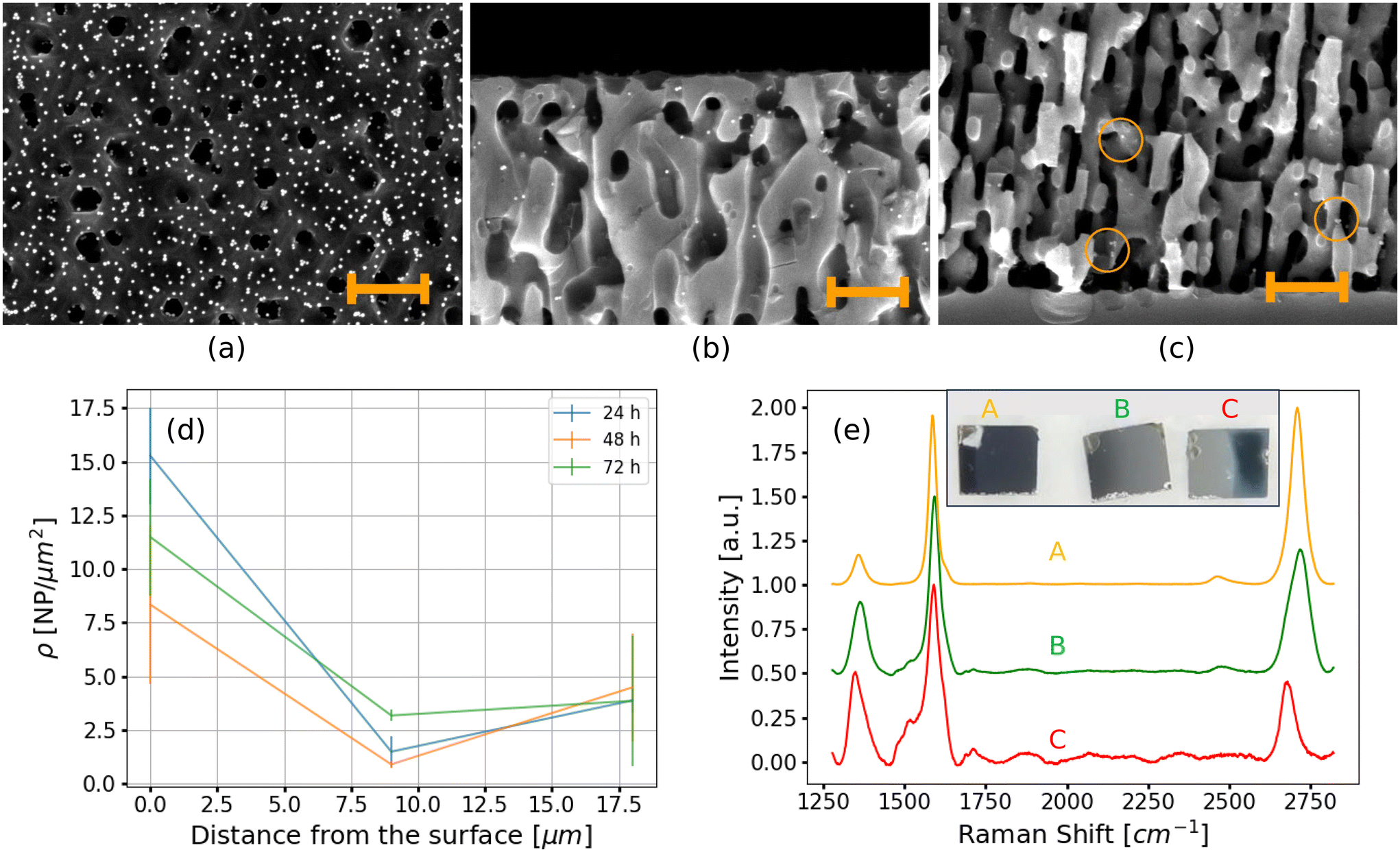 | ||
| Fig. 1 (a) Top-view SEM image of an AuNP-functionalized 3DG sample. (b) and (c) Cross-sectional SEM images of the top and the bottom regions of the porous layer, respectively. In the image of the bottom region, some of the NPs are circled in orange. In all images, the orange scale bar indicates 0.5 μm. (d) Trend of the NP density in the pores at different depths for different immersion times (24, 48, and 72 hours). (e) Raman spectra acquired in the three distinct regions of a sample (A, B, and C) revealing a graphene quality gradient. The inset shows an optical image of the 3DG sample cleaved into three pieces, exhibiting a color gradient. | ||
Furthermore, when immersing the 3DG sample in the solution of NPs under ultrasonication, we observed that the density of NPs was reduced by one order of magnitude (refer to Fig. S5†). This suggests that the vibration, instead of promoting the diffusion of NPs inside the pores, provides kinetic energy to the NPs sufficient to detach them from graphene.
Thus, we have established that a long immersion time in the solution of NPs under static conditions is the best method for the functionalization of 3DG. Therefore, we tested longer immersion times of 48 and 72 hours. Fig. 1d shows the NP density inside the pores as a function of depth obtained for 24, 48, and 72 hours of immersion in the solution of NPs. Since no significant increase in the nanoparticle density was observed, we concluded that 24 hours is sufficient time for the diffusion of NPs.
Graphenizing a sample in a non-homogeneous manner allowed us to study the role of graphene quality in the functionalization. The non-homogeneous graphenization was achieved by inducing a thermal gradient along the sample in order to have one side at the optimal growth temperature and the opposite side at a temperature more than 50 K colder (see the Methods section). The sample was functionalized by immersing it in the solution of NPs for 24 hours prior to cleavage. Then, it was cleaved into three pieces labeled “A”, “B”, and “C”.
The inset of Fig. 1e shows an optical picture of this sample (after cleavage), in which a color gradient is clearly visible. Besides, three Raman spectra, acquired on each piece of the sample before the functionalization, are also shown. For each region, the spectrum is the average of several spectra acquired over a 21 × 21 μm2 map. Considering the common Raman spectroscopy benchmarks of graphene, it emerges that in the “A” region, where the optimal temperature was achieved, state-of-the-art 3DG has been grown, exhibiting an I(2D)/I(G) intensity ratio of 1.7 and an I(G)/I(D) intensity ratio of 4.8 (consistent with that reported in the ESI, Fig. S2a†). Moving towards the “C” region, the graphene quality was degraded. The I(2D)/I(G) intensity ratio was reduced to 0.4 because of the reduction in graphene coverage. Concurrently, due to the higher density of defects in region “C”, the I(G)/I(D) intensity ratio decreased to 1.9.
After the functionalization, we investigated the surfaces of the “A” and “C” regions by SEM, as well as the cross-sections between “A” and “B”, and “B” and “C”. We observed a sharp decrease in the NP densities from “A” to “C”: the top-surface density was about six times smaller in “C” (σ ≃ 34 NPs μm−2), while the density inside the pores was reduced by about a factor of four to ρtop ≃ 3.9 NPs μm−2. Thus, high graphene coverage and quality promote the functionalization process.
Interestingly, the resistivity of the 3DG samples decreases after functionalization (for more details, refer to Fig. S6†).
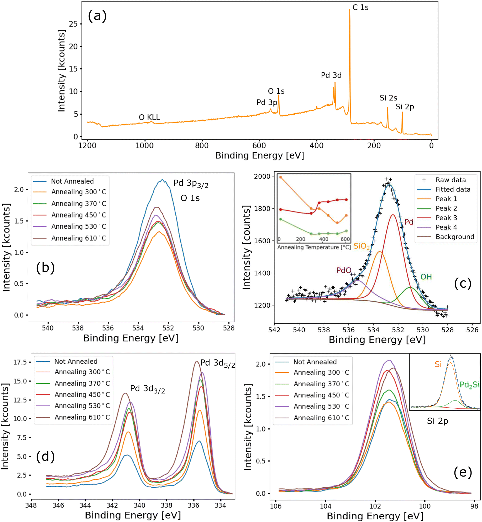
Furthermore, the AuNP-functionalized 3DG was analyzed by XPS measurements. Fig. 2a shows a wide-scan photoemission spectrum of a 3DG sample right after functionalization. The C 1s peak is the most prominent, since carbon is the main constituent of the sample's surface. Silicon peaks, originating from SiC, are clearly visible, as well as gold peaks, which confirm the presence of Au on the surface after functionalization. Oxygen is also observed (the O 1s peak and the O KLL Auger peak), since the sample has been exposed to air before the XPS measurements. No contaminants are detected, except for a weak Na signal (coming from the sodium citrate capping layer of the AuNPs). Fig. 2b–e shows the fits of high-resolution spectra of the core levels of C 1s, O 1s, Si 2p, and Au 4f, respectively. The carbon spectrum (cf.Fig. 2b) is fitted with three components typical of epitaxial graphene grown on SiC.41 The main component, positioned at 284.5 eV (peak 1), is due to the graphene sp2 C atoms. The shoulder at higher binding energy (at 285.5 eV, peak 3) is due to the buffer layer sp3 C atoms, and the shoulder at 283.1 eV (peak 2) is due to C–Si bonds.41 The oxygen spectrum (cf.Fig. 2c) is fitted with two components. The higher binding energy component, centered at 533.2 eV (peak 2), is assigned to the superposition of O–C![[double bond, length as m-dash]](https://www.rsc.org/images/entities/char_e001.gif) O bonds (due to the citrate in the capping layer of the NPs) and SiO2, while the other component, centered at around 531.9 eV (peak 1), is assigned to the –OH group (due to adsorbed water).42 The Si spectrum (cf.Fig. 2d) is fitted with two p curves with a fixed spin–orbit splitting of 0.63 eV. The main component, centered at 100.9 eV (peak 1), is due to Si–C in silicon carbide. The small component centered at around 102.1 eV (peak 2) is attributed to SiO2.43 The Au 4f signal (cf.Fig. 2e) is fitted with a single doublet having fixed spin–orbit splitting of 3.7 eV and the 4f7/2 component centered at around 84.05 eV.
O bonds (due to the citrate in the capping layer of the NPs) and SiO2, while the other component, centered at around 531.9 eV (peak 1), is assigned to the –OH group (due to adsorbed water).42 The Si spectrum (cf.Fig. 2d) is fitted with two p curves with a fixed spin–orbit splitting of 0.63 eV. The main component, centered at 100.9 eV (peak 1), is due to Si–C in silicon carbide. The small component centered at around 102.1 eV (peak 2) is attributed to SiO2.43 The Au 4f signal (cf.Fig. 2e) is fitted with a single doublet having fixed spin–orbit splitting of 3.7 eV and the 4f7/2 component centered at around 84.05 eV.
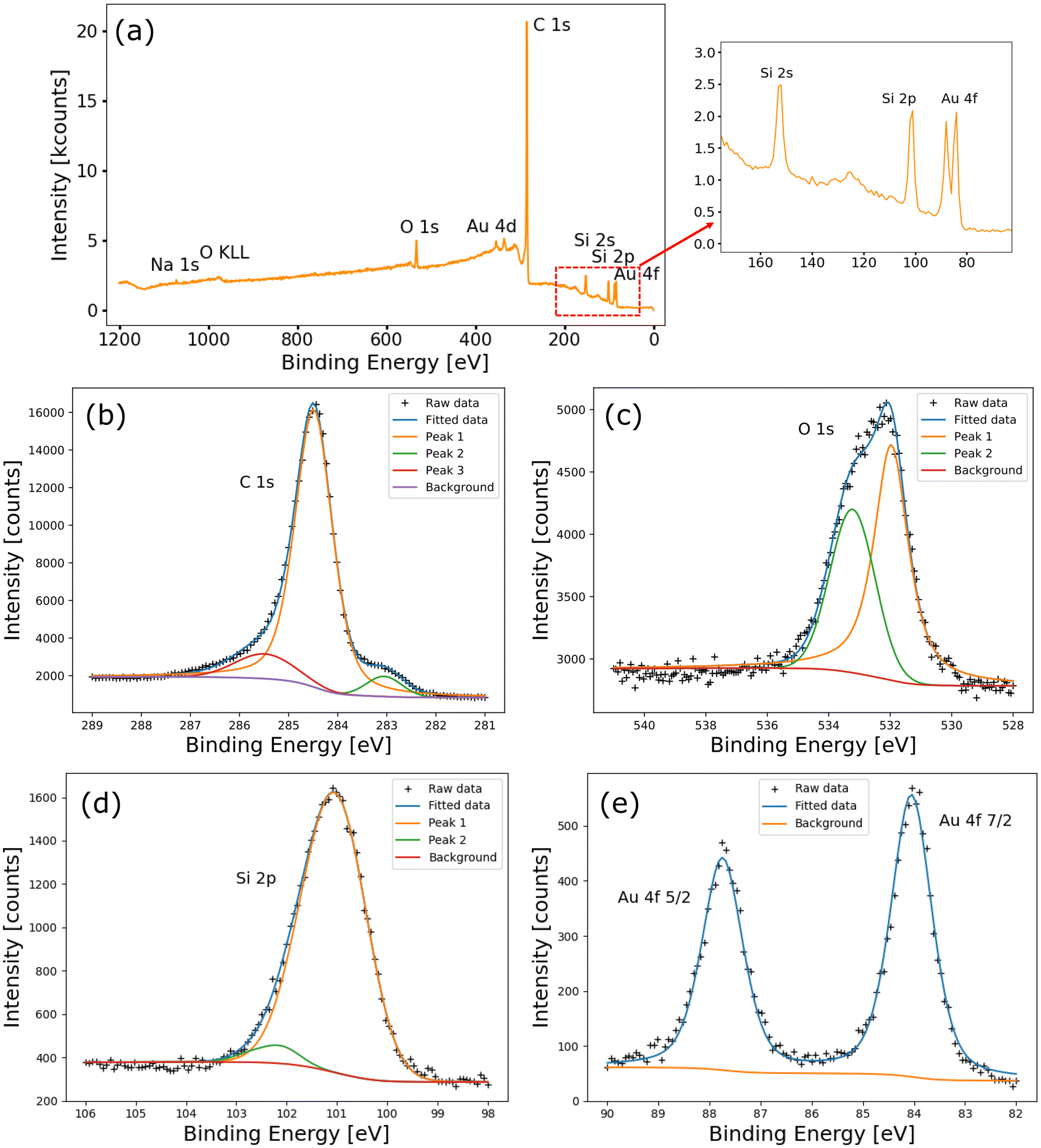 | ||
| Fig. 2 (a) Photoemission spectrum of an AuNP-functionalized 3DG sample prior to annealing. A close-up on the Si peaks and the Au 4f peak is also shown. (b–e) XPS fits of the spectra of AuNP-functionalized 3DG prior to annealing. The fitted Shirley background signal is also plotted. (b) Fit of the C 1s spectrum. Graphene contributes to peak 1, SiC contributes to peak 2, and the sp3 C atoms of the buffer layer contribute to peak 3. (c) Fitted O 1s spectrum. Peak 1 is assigned O–CO superimposed to SiO2, while peak 2 is assigned to –OH. (d) Si 2p spectrum fitted with two doublets with a fixed spin–orbit splitting of 0.63 eV, one due to Si–C (peak 1) and the other due to SiO2 (peak 2). (e) Au 4f spectrum fitted with a single doublet with a fixed spin–orbit splitting of 3.7 eV. | ||
After these measurements, a series of annealing steps at increasing temperatures was performed, followed each time by a new set of XPS measurements. The annealing processes were performed under UHV conditions in the same chamber as the XPS measurements. The annealing temperatures were 200, 350, 460, and 530 °C.
Fig. 3a shows high-resolution spectra of the C 1s core level acquired after each of the annealing steps. 3DG is known to be thermally stable within this range of temperatures,6 and consistently the carbon spectra remain unaltered with increasing annealing temperature. Similarly, the Si 2p spectra (cf.Fig. 3b) are almost unchanged by the annealing. This indicates that no gold silicide forms during the thermal treatments. Fig. 3c shows O 1s spectra acquired after each of the annealing steps. Upon increasing the annealing temperature, the signal sharply decreases. This is due to water desorption and the degradation of the capping layer of the NPs. At the annealing temperature of 350 °C, only one peak, positioned at 533.2 eV, is observed and this is attributed to SiO2, since the capping layer is mostly decomposed.44 In addition, above the annealing temperature of 350 °C, a small signal emerged at 530.8 eV, attributed to indium oxide. Indium is used to attach the samples to the sample holder in the XPS chamber. Indeed, the In 3d peak is also visible in wide scans after annealing above 350 °C, but is not reported here. Thus, the weak In signal is imputed to a spurious contribution from the edges of the sample. Finally, the intensities of peaks in the Au 4f spectra increase with increasing annealing temperature, as shown in Fig. 3d. This is a consequence of the gradual decomposition of the capping layer of the NPs (which, when present, attenuates the gold signal). Except for the intensity increase, the peaks do not change with temperature, and the positions of the peaks are constant. This is further confirmation of the absence of Si–Au bonds, which otherwise should appear in the Au 4f photoemission signal at higher binding energy.45 In conclusion, AuNP-functionalized 3DG is thermally stable up to a temperature of at least 530 °C.
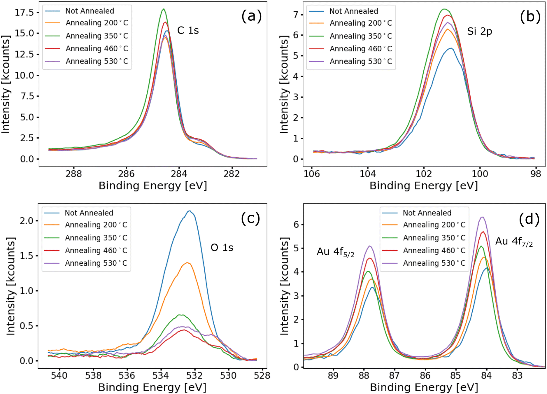 | ||
| Fig. 3 (a), (b), (c) and (d) Comparison of the C 1s, Si 2p, O 1s, and Au 4f spectra, respectively, acquired after annealing the Au-functionalized 3DG sample at different temperatures. | ||
Functionalization with palladium nanoparticles
Palladium was chosen since it is a very versatile metal with applications in the fields of catalysis,46 sensors,47 and energy storage and conversion.48Palladium nanoparticles (PdNPs) were synthesized in house following two different procedures described in the Methods section. The first PdNPs we synthesized and studied were SDS-PdNPs, where SDS refers to sodium dodecyl sulphate involved in the NP synthesis. After the synthesis, the NPs were dispersed on a SiO2 substrate and characterized by AFM (see Fig. S7a†). The resulting NPs are found to be spherical and monodispersed with an average diameter of 8.0 ± 1.5 nm.
As for the AuNPs, we proceeded to functionalize a 3DG sample with the SDS-PdNPs by immersion in the nanoparticle solution for 24 h. Then, the functionalized sample was analyzed by SEM. The functionalization was successful since a large number of NPs were detected on the sample. We also observed a non-homogeneous distribution of NPs over the 3DG surface and a tendency of clustering (SEM images of SDS-PdNP-functionalized 3DG are shown in Fig. S7b†). Another aspect that emerged from energy dispersive X-ray spectroscopy (EDX) measurements performed on this sample is the presence of sulfur at the position of the palladium nanoparticles. Sulfur was still detectable after annealing the sample at 800 °C (for more details, refer to Fig. S8†). The presence of sulfur is due to the decomposition of the capping layer of the NPs. Since sulfur poisoning of palladium is well known to inhibit the catalytic activity of palladium, or its capability to adsorb other elements,49,50 this condition should be avoided. Additionally, we observed that the decomposition of the capping layer of the NPs produces amorphous carbon regions on the sample surface.
To avoid NP clustering and sulfur poisoning, a new synthesis procedure was adopted (as described in the Methods section). PVP-PdNPs (where PVP refers to poly(N-vinyl-2-pyrrolidone) adopted in the synthesis of NPs) are not subject to sulfur poisoning, since no sulfur is involved in their synthesis. In addition, PVP-PdNPs possess a capping layer made of shorter molecules compared to that of the SDS-PdNPs, i.e., with fewer carbon atoms. This implies reduction in the carbon residues over the sample surface upon thermal degradation of the capping agent.
After the synthesis, the PVP-PdNPs were characterized by AFM to determine their dimension, shape, and dispersion. For the measurements, the nanoparticles were drop-cast onto a SiO2 substrate. Fig. 4a shows an AFM image of PVP-PdNPs over the SiO2 support. They appear spherical with an average diameter of 7.2 ± 3.0 nm. Moreover, clustering of NPs is almost absent.
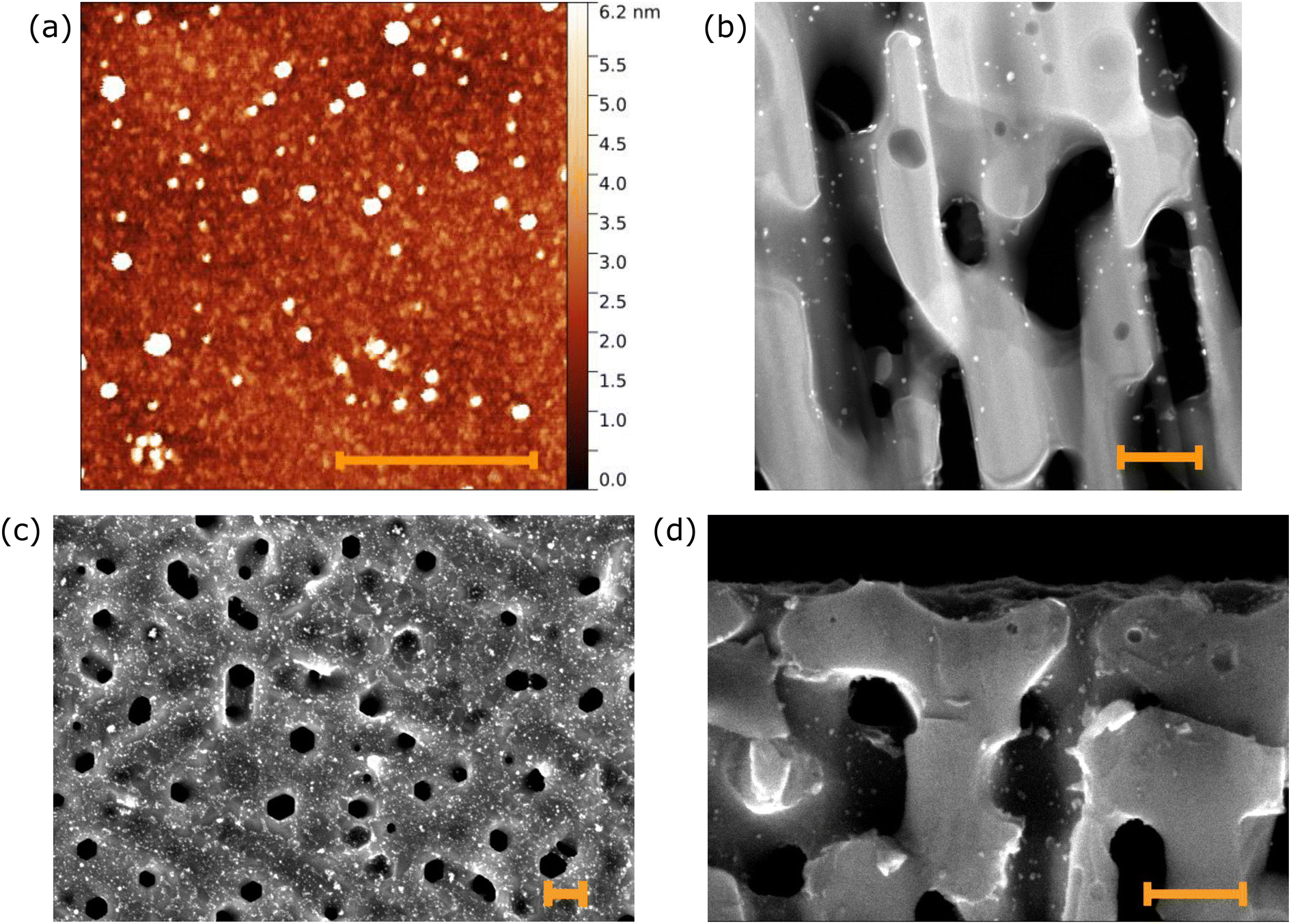 | ||
| Fig. 4 (a) AFM image of PVP-PdNPs deposited on an SiO2 substrate. The measurement was conducted after annealing the sample at 230 °C for 4 hours to decompose the NP capping layer. The spatial resolution of the AFM is higher along the out-of-plane direction than along the in-plane directions, thus the NPs appear laterally broadened, while their height accurately measures their diameter. (b) HAADF-STEM cross-sectional image of a 3DG sample functionalized with PVP-PdNPs. PVP-PdNPs appear as bright spots on the walls of the pores. (c) and (d) SEM images of a 3DG sample functionalized with PVP-PdNPs in the top view and cross-section, respectively. The scale bar in (a)–(d) indicates 200 nm. | ||
The functionalization of 3DG was also performed with the PVP-PdNPs by immersing the samples in the solution of NPs (0.1 mg ml−1) for 24 hours. After drying the samples in air, HAADF-STEM and SEM measurements were performed.
Fig. 4b shows an HAADF-STEM image acquired in cross-section on a thin lamella of the sample prepared via focused ion beam (FIB) milling. Palladium nanoparticles are clearly visible as bright spots in the HAADF-STEM image. EDX maps (Fig. S9†) confirmed that these NPs are composed of Pd. PVP-PdNPs are evenly distributed over the walls of the pores; however, their density decreases with increasing depth, as observed for the AuNP-functionalized samples. To determine the population of NPs across the surface, we analyzed in detail the top and bottom parts of the cross-section (refer to Fig. S10†) by TEM. In the first 750 nm below the surface, we have identified 155 NPs over a 750 × 750 nm2 scanned area, which corresponds to a density ρ = 276 NPs μm−2. Between 0.75 μm and 1.5 μm below the surface, we measured a density ρ = 98 NPs μm−2. Thus, the estimated loading of Pd is ∼420 wt% and ∼1 wt% with respect to graphene and the SiC substrate, respectively. Additionally, we performed electron tomography on the thin lamella over a tilt range of 80° to evaluate the pore connection (refer to Fig. S11†). The pores have an average size diameter of 90 nm, which is one order of magnitude larger than the size of the NPs. This allows particles to diffuse through the porous structure.
Fig. 4c and d shows SEM images of the top surface and cross-section, respectively. Unlike the SDS-PdNPs, the PVP-PdNPs appear well distributed over the sample surface and clustering is absent, as shown in Fig. 4c. Even if the PVP-PdNPs are smaller than the AuNPs, they exhibit good contrast in the SEM images. This was different for SDS-NPs, because their longer capping molecules shielded Pd, sharply reducing the contrast. This improved contrast allowed us to observe PdNPs inside the pores also via SEM, as shown in Fig. 4d, and to estimate their density. The nanoparticle top surface density is σ = 3500 ± 740 NPs μm−2, while, in the first 1 μm below the surface, the density inside the pores is ρ = 172 ± 64 NPs μm−2. The larger relative errors in the NP densities as compared to the AuNPs are a consequence of the smaller size of the Pd NPs. The NP density inside the pores measured via SEM (computed over a large set of different measurements) is in good agreement with the results obtained by HAADF-STEM. This comparison demonstrates the validity of SEM evaluation performed in a depth range that includes both areas investigated by HAADF-STEM.
Importantly, both HAADF-STEM and SEM measurements demonstrate that the PdNP densities are more than one order of magnitude greater than the AuNP densities. There is evidence that smaller nanoparticles are more likely to diffuse inside the pores of 3DG and to stick to their surfaces. In addition, from the nanoparticle density we extract a loading of ∼2970 wt% over the top surface with respect to graphene. Considering the lower mass density of Pd (12.0 g cm−3) compared to Au (19.3 g cm−3), the volume of the deposited metal is comparable for AuNP and PdNP functionalization.
The PVP-PdNP-functionalized 3DG was also analyzed by XPS. Fig. 5a shows a wide photoemission spectrum of a 3DG sample just after functionalization. The C 1s peak is the most intense, as it is for the Au-functionalized sample. Si 2p and 2s peaks are observed as well. The palladium signal, in particular the 3d peaks, exhibits an intensity similar to that of the silicon peaks. Even considering the difference in the photoionization cross-section between Pd and Si, this is a clear indication of large amounts of Pd being deposited on the sample, confirming the successful functionalization. Also oxygen is detected (O 1s and O KLL Auger peaks), consistent with the exposure of the sample to air prior to spectroscopic measurements; contaminants were not detected.
 | ||
| Fig. 5 (a) Wide photoemission spectrum of a PVP-PdNP-functionalized 3DG sample prior to annealing. (b) Comparison of the spectra acquired after each annealing step in the binding energy range of O 1s and Pd 3p3/2. (c) Fit of the spectrum acquired after the last annealing step of (b). Data are fitted with 4 curves. Peak 1 is attributed to the convolution of SiO2 and OC emission, peak 2 is attributed to –OH, while palladium metal and palladium oxide contribute to peak 3 and peak 4, respectively. Inset: intensities of peaks 1, 2, and 3 as a function of annealing temperature. (d) Comparison of the Pd 3d spectra acquired after each annealing step. (e) Comparison of the Si 2p spectra acquired after each annealing step. Inset: the spectrum acquired after the last annealing step fitted with two components, i.e., Si–C and Pd2Si. | ||
As for the AuNP-functionalized sample, after the initial set of measurements, a series of annealing steps were performed on the sample. The thermal treatments were performed under UHV conditions. Each annealing step was followed by a new set of XPS measurements without breaking the vacuum. The explored annealing temperatures were 300, 370, 450, 530, and 610 °C.
As for the Au-functionalized sample, variations in the C 1s spectra with increasing annealing temperature are not observed (shown in Fig. S12†). Fig. 5b shows the spectra acquired after each annealing step in the binding energy range of both the O 1s and Pd 3p3/2 peaks. Therefore, the signal has been fitted with four components: two for oxygen (as for AuNP-functionalized samples), one for Pd, and one for PdO. Fig. 5c shows the fit of the spectrum acquired after the last annealing, while the inset shows the intensity of the four components as a function of annealing temperature. Prior to annealing, most of the signals are due to oxygen peaks. After the first annealing, a sharp drop in the oxygen signal is observed, which is compatible with water desorption. Upon increasing the annealing temperature, the palladium peak, positioned at 532.4 eV, became dominant. Indeed, the PVP capping layer starts to decompose at around 350 °C,51 which results in reduction of the palladium signal attenuation and thus an increase in the intensity of the Pd 3p3/2 peak. During the decomposition of the capping layer, some of the released oxygen atoms are available for Pd oxidation. Therefore, the PdO contribution is negligible up to an annealing temperature of 370 °C.
Fig. 5d shows Pd 3d spectra at different annealing temperatures. Similar to the Pd 3p3/2 peak, the Pd 3d peak intensity increases with annealing temperature. In addition, after annealing at 610 °C, the Pd 3d core level emission shifts by 0.2 eV to higher binding energy. This is understood by fitting the core level with two components for palladium metal and palladium silicide.52 The 3d5/2 peak of palladium metal is centered at 335.5 eV, while for the silicide it is 1.1 eV higher. The palladium silicide signal is negligible up to 530 °C. Instead, after the last annealing step at 610 °C, it became non-negligible, resulting in a blue-shift of the peaks.
The silicide formation is further confirmed by the Si 2p spectra, which are shown in Fig. 5e. Similar to Pd 3p, the Si 2p peak position is constant at 101.2 eV with increasing annealing temperature up to 530 °C, while, after the last annealing step, the peak is red-shifted by 0.2 eV. This is compatible with the appearance of a lower energy peak, centered at 100.6 eV, due to Pd2Si formation53 (as shown in the inset of Fig. 5e).
In conclusion, PVP-PdNP functionalization of 3DG is a clean process (no contaminants are detected), which leads to high coverage of NPs over the sample surface. In addition, the as-produced samples are observed to be thermally stable up to a temperature of 530 °C, above which silicide formation indicates a reaction of the PdNPs with the substrate. Moreover, the stability of the system is further confirmed by STM measurements performed on the PVP-PdNP-functionalized 3DG after several thermal treatments in which no agglomeration of the NPs is observed (cf. Fig. S13†).
Conclusions
We have demonstrated a method for the successful functionalization of epitaxial 3DG with metal (gold and palladium) nanoparticles. This method does not induce any chemical reaction at the substrate surface, and the functionalization is driven by the diffusion of nanoparticles and their subsequent sticking to the pore walls via electrostatic and van der Waals interactions. Therefore, our approach can be applied to any kind of nanoparticles, even non-metallic, or in shapes different from spherical. The diffusion can be promoted by utilizing smaller NPs or larger pores. Considering the ease in obtaining successful functionalization and the wide range of usable nanoparticles, our results pave the way to numerous future studies on this new class of materials.We demonstrated the fundamental role of graphene in the functionalization. In fact, for samples that exhibit low graphene coverage, or low quality of 3DG, a sharp reduction in NP density was observed.
Through XPS measurements we established that the method is clean and no contaminants are detected over the functionalized 3DG samples. XPS provided information on the thermal stability of the system: 3DG functionalized with gold or palladium is stable up to at least 530 °C. This feature could be exploited for high-temperature catalytic reactions.
Through EDX we were able to detect the sulfur poisoning of palladium in SDS-PdNPs. We observed that the poisoning was not removed by annealing the sample at 800 °C. Therefore, we adopted a routine sulfur-free synthesis. This method also guaranteed much less clustering of NPs, their more homogeneous distribution over the 3DG surface, and reduction in residual carbon from the thermal degradation of their capping molecules (since they are shorter).
In conclusion, we realized a versatile support that could be employed in a wide range of fields. Au-decorated 3DG could be used as a substrate for surface-enhanced Raman spectroscopy. Pd-functionalized 3DG can achieve great performance in hydrogen sensing and storage. In general, this new class of materials is suitable for a multitude of catalytic applications, even in harsh environments, and they can be tuned by selecting an appropriate metal for the specific reaction. Moreover, these materials could also find applications in biological tissue engineering since graphene and SiC are biocompatible.54,55
Methods
Porous silicon carbide fabrication
In the present study, n-doped single-crystal 4H-SiC wafers are used (purchased from SiCrystal). They are 350 μm thick and possess a bulk resistivity of 0.02 Ω cm. All porousification processes were performed on the (0001) Si-face of SiC wafer.The porousification of wafers was achieved by photoelectrochemical etching. The etching procedure comprises three steps: first metal-assisted photochemical etching (MAPCE),56 then photo electrochemical etching (PECE), and finally, a second MAPCE step. Prior to the first MAPCE step, wafers were cleaned by inverse sputter etching using LS730S von Ardenne sputter equipment for 150 s. Without breaking the vacuum, 300 nm thick platinum pads were sputter deposited at the wafer edges (these act as local cathodes during the etching). Then, the sample was transferred to an electrochemical cell for 30 minutes of MAPCE. Here, the utilized etching solution contains 1.31 mol l−1 HF and 0.15 mol l−1 H2O2. The cell is equipped with an 18 W UV source. The interface between SiC and the solution acts as the cathode. Here, SiC oxidises to SiO2, which was dissolved by HF, resulting in the formation of pores over the sample surface. The PECE solution is composed of 1200 ml of deionized water, 150 ml of HF (48%) and 150 ml of pure ethanol. The same UV lamp as that used in in MAPCE was utilized and a bias of 11.5 V was applied between the two sides of the sample. Because of the applied bias, PECE produces a more directional and deeper porousification. To guarantee a homogeneous porousification,27 after PECE, a second MAPCE step was performed under the same conditions as the first step, except for a longer time of 1 hour.
Three-dimensional graphene growth
The porousified SiC wafers were cut into pieces (2 × 8 mm2) using a wafer saw. Pieces were individually transferred to an ultra-high vacuum (UHV) chamber (base pressure 10−10 mbar) where they were degassed overnight at 1000 K. After the degassing, the samples were cooled to room temperature (RT) and heated again to 1650 K to allow graphene formation on the surface of the pores. After 150 s of annealing, the sample was allowed to cool down to RT.Veronesi et al. observed that the temperature reached by the sample during the annealing depends on the quality of the mechanical contact between the sample and the sample holder.26 Therefore, by clamping one side of the sample more firmly than the other, we obtained the non-homogeneous graphenized sample discussed in the Functionalization with gold nanoparticles section.
Palladium nanoparticle synthesis
All chemicals were purchased from Sigma-Aldrich unless otherwise indicated and used without further purification. Ultrapure water purified using a Millipore Milli-Q water system was used to prepare aqueous solutions.SDS-PdNPs were synthesized from an aqueous solution of palladium(II) acetate (Pd(OAc)2, 98% pure) and sodium dodecyl sulphate (SDS, >99% pure). SDS was dispersed in MilliQ water to a concentration 0.05 M. Therein, 10 mg of Pd(OAc)2 was dissolved. The obtained solution was transferred to a three-neck flask equipped with a reflux condenser. The solution was heated to 100 °C under magnetic stirring for 6 hours. The heat induces the thermal decomposition of SDS to 1-dodecanol. This, in turn, induces the formation of PdNPs upon reduction of Pd2+ ions and oxidation of 1-dodecanol to dodecanoic acid, which acts as a stabilizer for the produced nanoparticles.57 Once the reaction is terminated, the solution was cooled to RT. The PdNPs were collected by ultrahigh speed centrifugation (13![[thin space (1/6-em)]](https://www.rsc.org/images/entities/char_2009.gif) 000 rpm) for 10 minutes and washed sequentially with water and ethanol (supplied by Carlo Erba Reagents) to remove excess surfactant. Finally, the SDS-PdNPs were dispersed in ethanol and stored at −20 °C.
000 rpm) for 10 minutes and washed sequentially with water and ethanol (supplied by Carlo Erba Reagents) to remove excess surfactant. Finally, the SDS-PdNPs were dispersed in ethanol and stored at −20 °C.
PVP-PdNPs were synthesized following the polyol method in which an alcohol is used for the reduction of the metal precursor.58 A capping agent is required to prevent clustering of the nanoparticles. Poly(N-vinyl-2-pyrrolidone) (PVP) was chosen as the capping agent for our synthesis since it is known that the carbonyl groups of PVP partly coordinate to the surface Pd atoms of the Pd nanoparticles.59 Furthermore, part of the main chain of PVP is expected to be adsorbed on the surface Pd atoms by hydrophobic interaction.
In this synthesis, 0.0205 g (0.09 mmol, 10 mM) of Pd(OAc)2 was dissolved in 1.5 ml of ethylene glycol (EG, >99% pure) under magnetic stirring and ambient conditions for 2 h. During this process, the solution turns from light orange to dark brown, indicating the formation of PdNPs. In a second vial, 0.05 g of PVP (average molecular weight 40000) was dissolved in 3 ml of EG and stirred for 2 h. Into a three-neck flask, equipped with a reflux condenser, 5 ml of EG was poured. The EG in the flask was heated to 160 °C under magnetic stirring. Aliquots of the PdNP solution (30 μl) and the PVP solution (60 μl) were injected into the flask every 30 s (50 additions in total). Then, the flask was cooled to RT and the obtained suspension was centrifuged at 13000 rpm for 10 minutes to remove the precipitate containing large nanoparticles (diameters above ∼80 nm). The smaller nanoparticles (diameter ≲ 10 nm) were instead suspended in the supernatant. These were collected by dilution of the solution with acetone (>99% pure) and centrifugation. The product was washed with acetone three times to remove most of the EG and the excess PVP. Finally, the PVP-PdNPs were dispersed in ethanol and stored at −20 °C.
Measurements
Raman spectroscopy of pristine 3DG samples was performed utilizing an inVia confocal Raman microscope (equipped with a 532 nm laser with a spot diameter of 1 μm) from Renishaw. STM characterization of the pristine material was performed with a VT-UHV STM from RHK. The AFM characterization of PdNPs (on SiO2 substrates) was conducted in tapping mode using a Dimension Icon from Bruker.The functionalized sample was investigated in cross-section via high-angle annular dark-field scanning transmission electron microscopy (HAADF-STEM). The analysis was conducted using an X-Ant-EM Titan microscope operating at 300 kV equipped with an aberration corrector and a monochromator. Prior to HAADF-STEM measurements, the sample was milled into lamellae via focused ion beam (FIB) milling. Electron tomography was performed using a Fischione model 2020 single tilt holder. The ML-EM algorithm implemented in the ASTRA Toolbox60 was employed for volume reconstruction.
For SEM measurements conducted on the functionalized 3DG sample, a FEG-SEM Merlin from ZEISS was used.
The EDX measurements of sulfur poisoning of palladium were performed using a QUANTAX EDS from Bruker (mounted to an Ultra Plus FE-SEM from ZEISS).
XPS characterization of the 3DG samples functionalized with AuNPs and PVP-PdNPs was performed using a Surface Science Instrument SSX-100-301 spectrometer operating with an Al Kα X-ray source with an overall energy resolution of 0.9 eV.
Data availability
The data supporting this article have been included as part of the ESI.†Conflicts of interest
There are no conflicts to declare.References
- G. T. M. Kadja, M. M. Ilmi, N. J. Azhari, M. Khalil, A. T. N. Fajar, Subagjo, I. G. B. N. Makertihartha, M. L. Gunawan, C. B. Rasrendra and I. G. Wenten, J. Mater. Res. Technol., 2022, 17, 3277–3336 CrossRef CAS
.
- A. Memetova, I. Tyagi, L. Singh, R. R. Karri, Suhas, K. Tyagi, V. Kumar, N. Memetov, A. Zelenin, A. Tkachev, V. Bogoslovskiy, G. Shigabaeva, E. Galunin, N. M. Mubarak and S. Agarwal, Sci. Total Environ., 2022, 838, 155943 CrossRef CAS PubMed
- H. Moradi, M. Zhoulideh and M. Ghafariasl, Opt. Commun., 2023, 542, 129592 CrossRef CAS
- K. Singh, N. A. Travlou, S. Bashkova, E. Rodríguez-Castellón and T. J. Bandosz, Carbon, 2014, 80, 183–192 CrossRef CAS
- S. Veronesi, Y. Vlamidis, L. Ferbel, C. Marinelli, C. Sanmartin, I. Taglieri, G. Pfusterschmied, M. Leitgeb, U. Schmid, F. Mencarelli and S. Heun, J. Sci. Food Agric., 2023 DOI:10.1002/jsfa.13118
- A. Macili, Y. Vlamidis, G. Pfusterschmied, M. Leitgeb, U. Schmid, S. Heun and S. Veronesi, Appl. Surf. Sci., 2023, 615, 156375 CrossRef CAS
- H. Shao, Y.-C. Wu, Z. Lin, P.-L. Taberna and P. Simon, Chem. Soc. Rev., 2020, 49, 3005–3039 RSC
- M. Mabrouk, R. Rajendran, I. E. Soliman, M. M. Ashour, H. H. Beherei, K. M. Tohamy, S. Thomas, N. Kalarikkal, G. Arthanareeswaran and D. B. Das, Pharmaceutics, 2019, 11, 294 CrossRef CAS PubMed
- W. Tian, H. Zhang, X. Duan, H. Sun, G. Shao and S. Wang, Adv. Funct. Mater., 2020, 30, 1909265 CrossRef CAS
- M. Ni, L. Zhou, Y. Liu and R. Ni, Front. Chem., 2023, 11, 1205280 CrossRef CAS PubMed
- M. G. Mohamed, M. M. Samy, T. H. Mansoure, C.-J. Li, W.-C. Li, J.-H. Chen, K. Zhang and S.-W. Kuo, Int. J. Mol. Sci., 2021, 23, 347 CrossRef PubMed
- H. Funabashi, S. Takeuchi and S. Tsujimura, Sci. Rep., 2017, 7, 45147 CrossRef CAS PubMed
- K. S. Novoselov, A. K. Geim, S. V. Morozov, D. Jiang, Y. Zhang, S. V. Dubonos, I. V. Grigorieva and A. A. Firsov, Science, 2004, 306, 666–669 CrossRef CAS PubMed
- K. I. Bolotin, K. J. Sikes, Z. Jiang, M. Klima, G. Fudenberg, J. Hone, P. Kim and H. L. Stormer, Solid State Commun., 2008, 146, 351–355 CrossRef CAS
- A. A. Balandin, Nat. Mater., 2011, 10, 569–581 CrossRef CAS PubMed
- C. Lee, X. Wei, J. W. Kysar and J. Hone, Science, 2008, 321, 385–388 CrossRef CAS PubMed
- S. Zhang, H. Wang, J. Liu and C. Bao, Mater. Lett., 2020, 261, 127098 CrossRef CAS
- L. Jiang and Z. Fan, Nanoscale, 2014, 6, 1922–1945 RSC
- Y. Ma and Y. Chen, Natl. Sci. Rev., 2014, 2, 40–53 CrossRef
- Z. Chen, W. Ren, L. Gao, B. Liu, S. Pei and H.-M. Cheng, Nat. Mater., 2011, 10, 424–428 CrossRef CAS PubMed
- M. Yu, Y. Huang, C. Li, Y. Zeng, W. Wang, Y. Li, P. Fang, X. Lu and Y. Tong, Adv. Funct. Mater., 2015, 25, 324–330 CrossRef CAS
- X. Xu, L. Pan, Y. Liu, T. Lu, Z. Sun and D. H. C. Chua, Sci. Rep., 2015, 5, 8458 CrossRef CAS PubMed
- Z. Su, X. Xu, Y. Cheng, Y. Tan, L. Xiao, D. Tang, H. Jiang, X. Qin and H. Wang, Nanoscale, 2019, 11, 962–967 RSC
- M. A. Worsley, P. J. Pauzauskie, T. Y. Olson, J. Biener, J. H. Satcher and T. F. Baumann, J. Am. Chem. Soc., 2010, 132, 14067–14069 CrossRef CAS PubMed
- Y. Xu, K. Sheng, C. Li and G. Shi, ACS Nano, 2010, 4, 4324–4330 CrossRef CAS PubMed
- S. Veronesi, G. Pfusterschmied, F. Fabbri, M. Leitgeb, O. Arif, D. A. Esteban, S. Bals, U. Schmid and S. Heun, Carbon, 2022, 189, 210–218 CrossRef CAS
- M. Leitgeb, C. Zellner, C. Hufnagl, M. Schneider, S. Schwab, H. Hutter and U. Schmid, J. Electrochem. Soc., 2017, 164, E337–E347 CrossRef CAS
- G. Gorgolis and C. Galiotis, 2D Mater., 2017, 4, 032001 CrossRef
- S. Heuser, N. Yang, F. Hof, A. Schulte, H. Schönherr and X. Jiang, Small, 2018, 14, 1801857 CrossRef PubMed
- Y. Xue, J. Xie, M. He, M. Liu, M. Xu, W. Ni and Y.-M. Yan, J. Mater. Chem. A, 2018, 6, 19210–19220 RSC
- Y. Ma, M. Zhao, B. Cai, W. Wang, Z. Ye and J. Huang, Biosens. Bioelectron., 2014, 59, 384–388 CrossRef CAS PubMed
- Y. Peng, J. Cao, J. Yang, W. Yang, C. Zhang, X. Li, R. A. W. Dryfe, L. Li, I. A. Kinloch and Z. Liu, Adv. Funct. Mater., 2020, 30, 2001756 CrossRef CAS
- P. S. Toth, M. Velický, Q. M. Ramasse, D. M. Kepaptsoglou and R. A. W. Dryfe, Adv. Funct. Mater., 2015, 25, 2899–2909 CrossRef CAS
- N. S. Nguyen, G. Das and H. H. Yoon, Biosens. Bioelectron., 2016, 77, 372–377 CrossRef CAS PubMed
- T. Mashoff, M. Takamura, S. Tanabe, H. Hibino, F. Beltram and S. Heun, Appl. Phys. Lett., 2013, 103, 013903 CrossRef
- L. Ferbel, S. Veronesi, Y. Vlamidis, A. Rossi, L. Sabattini, C. Coletti and S. Heun, FlatChem, 2024, 45, 100661 CrossRef CAS
- A. Moradi Golsheikh, N. M. Huang, H. N. Lim, R. Zakaria and C.-Y. Yin, Carbon, 2013, 62, 405–412 CrossRef CAS
- M. Lepesant, B. Bardet, L.-M. Lacroix, P. Fau, C. Garnero, B. Chaudret, K. Soulantica, T. Defforge, D. Valente, C. Andreazza, J. Billoué, P. Poveda and G. Gautier, Front. Chem., 2018, 6, 609 CrossRef CAS PubMed
- V. Amendola, R. Pilot, M. Frasconi, O. M. Maragò and M. A. Iatì, J. Phys.: Condens. Matter, 2017, 29, 203002 CrossRef PubMed
- D. Giljohann, D. Seferos, W. Daniel, M. Massich, P. Patel and C. Mirkin, Angew. Chem., Int. Ed., 2010, 49, 3280–3294 CrossRef CAS PubMed
- A. B. G. Trabelsi, F. V. Kusmartsev, M. B. Gaifullin, D. M. Forrester, A. Kusmartseva and M. Oueslati, Nanoscale, 2017, 9, 11463–11474 RSC
- B. Sivaranjini, R. Mangaiyarkarasi, V. Ganesh and S. Umadevi, Sci. Rep., 2018, 8, 8891 CrossRef CAS PubMed
- J. Guo, K. Song, B. Wu, X. Zhu, B. Zhang and Y. Shi, RSC Adv., 2017, 7, 22875–22881 RSC
- A. Marcilla, A. Gómez-Siurana, M. Beltrán, I. Martí-nez-Castellanos, I. Blasco and D. Berenguer, J. Sci. Food Agric., 2018, 98, 5916–5931 CrossRef CAS PubMed
- D. Ferrah, J. Penuelas, F. Boudaa, C. Botella, M. Silly, F. Sirotti and G. Grenet, J. Phys. Chem. C, 2022, 126, 18692–18703 CrossRef CAS
- M. Tanhaei, A. Mahjoub and R. Nejat, Catal. Lett., 2018, 148, 1549–1561 CrossRef CAS
- S. Mubeen, T. Zhang, B. Yoo, M. A. Deshusses and N. V. Myung, J. Phys. Chem. C, 2007, 111, 6321–6327 CrossRef CAS
- M. Luo, Y. Sun, Y. Qin, Y. Li, C. Li, Y. Yang, N. Xu, L. Wang and S. Guo, Mater. Today Nano, 2018, 1, 29–40 CrossRef
- J. Gabitto and C. Tsouris, Int. J. Chem. Eng., 2019, 2019, 1–12 CrossRef
- L. S. Escandón, S. Ordóñez, A. Vega and F. V. Díez, J. Hazard. Mater., 2008, 153, 742–750 CrossRef PubMed
- Y. K. Du, P. Yang, Z. G. Mou, N. P. Hua and L. Jiang, J. Appl. Polym. Sci., 2006, 99, 23–26 CrossRef CAS
- B. Krause, G. Abadias, C. Furgeaud, A. Michel, A. Resta, A. Coati, Y. Garreau, A. Vlad, D. Hauschild and T. Baumbach, ACS Appl. Mater. Interfaces, 2019, 11, 39315–39323 CrossRef CAS PubMed
- D.-X. Dai and I. Davoli, Vacuum, 1995, 46, 139–142 CrossRef CAS
- S. R. Shin, Y.-C. Li, H. L. Jang, P. Khoshakhlagh, M. Akbari, A. Nasajpour, Y. S. Zhang, A. Tamayol and A. Khademhosseini, Adv. Drug Delivery Rev., 2016, 105, 255–274 CrossRef CAS PubMed
- S. Saddow, Micromachines, 2022, 13, 346 CrossRef PubMed
- M. Leitgeb, C. Zellner, M. Schneider, S. Schwab, H. Hutter and U. Schmid, J. Phys. D: Appl. Phys., 2017, 50, 435301 CrossRef
- N. Karousis, G.-E. Tsotsou, F. Evangelista, P. Rudolf, N. Ragoussis and N. Tagmatarchis, J. Phys. Chem. C, 2008, 112, 13463–13469 CrossRef CAS
- I. Favier, D. Pla and M. Gómez, Chem. Rev., 2019, 120, 1146–1183 CrossRef PubMed
- A. Nemamcha, J.-L. Rehspringer and D. Khatmi, J. Phys. Chem. B, 2005, 110, 383–387 CrossRef PubMed
- W. van Aarle, W. J. Palenstijn, J. De Beenhouwer, T. Altantzis, S. Bals, K. J. Batenburg and J. Sijbers, Ultramicroscopy, 2015, 157, 35–47 CrossRef CAS PubMed
Footnote |
| † Electronic supplementary information (ESI) available. See DOI: https://doi.org/10.1039/d4nr01986e |
| This journal is © The Royal Society of Chemistry 2024 |