
 Open Access Article
 This Open Access Article is licensed under a
 Creative Commons Attribution 3.0 Unported Licence
On the origin of the improved hydrogen evolution reaction in Mn- and Co-doped MoS2†
Pasquale
Orgiani
 a,
Luca
Braglia
ab,
Vincent
Polewczyk
a,
Zhiwei
Nie
c,
Francesco
Lavini
d,
Shyni
Punathum Chalil
a,
Sandeep Kumar
Chaluvadi
a,
Piu
Rajak
a,
Floriana
Morabito
ab,
Edvard
Dobovičnik
e,
Vittorio
Foglietti
f,
Piero
Torelli
a,
Elisa
Riedo
d,
Regina
Ciancio
ab,
Nan
Yang
c and
Carmela
Aruta
*f
a,
Luca
Braglia
ab,
Vincent
Polewczyk
a,
Zhiwei
Nie
c,
Francesco
Lavini
d,
Shyni
Punathum Chalil
a,
Sandeep Kumar
Chaluvadi
a,
Piu
Rajak
a,
Floriana
Morabito
ab,
Edvard
Dobovičnik
e,
Vittorio
Foglietti
f,
Piero
Torelli
a,
Elisa
Riedo
d,
Regina
Ciancio
ab,
Nan
Yang
c and
Carmela
Aruta
*f
aCNR-IOM, Strada Statale 14, km 163, 5 Basovizza, Trieste 34149, Italy
bArea Science Park, Padriciano 99, Trieste 34149, Italy
cSchool of Physical Science and Technology, ShanghaiTech University, Shanghai 201210, China
dTandon School of Engineering, New York University, New York, NY 11201, USA
eDepartment of Engineering and Architecture, University of Trieste, Trieste 34127, Italy
fCNR-SPIN, via del Fosso del Cavaliere 100, Roma 00133, Italy. E-mail: carmela.aruta@spin.cnr.it
First published on 24th May 2024
Abstract
In the field of hydrogen production, MoS2 demonstrates good catalytic properties for the hydrogen evolution reaction (HER) which improve when doped with metal cations. However, while the role of sulfur atoms as active sites in the HER is largely reported, the role of metal atoms (i.e. molybdenum or the dopant cations) has yet to be studied in depth. To understand the role of the metal dopant, we study MoS2 thin films doped with Co and Mn ions. We identify the contribution of the electronic bands of the Mn and Co dopants to the integral valence band of the material using in situ resonant photoemission measurements. We demonstrate that Mn and Co dopants act differently: Mn doping favors the shift of the S–Mo hybridized band towards the Fermi level, while in the case of Co doping it is the less hybridized Co band that shifts closer to the Fermi level. Doping with Mn increases the effectiveness of S as the active site, thus improving the HER, while doping with Co introduces the metallic site of Co as the active site, which is less effective in improving HER properties. We therefore clarify the role of the dopant cation in the electronic structure determining the active site for hydrogen adsorption/desorption. Our results pave the way for the design of efficient materials for hydrogen production via the doping route, which can be extended to different catalytic reactions in the field of energy applications.
Introduction
Green hydrogen is emerging as one of the most viable clean energy sources to decarbonize our daily lives, industry and transportation. Thanks to the rapid growth of renewable energy sources, green hydrogen can be produced by water splitting electrolysis powered by energy obtained from clean energy sources that are intermittent or far from places of greatest demand. The water splitting reaction 2H2O ↔ 2H2 + O2 involves two half-reactions, namely the hydrogen evolution reaction (HER) and the oxygen evolution reaction (OER).The HER is a two-electron exchange reaction mechanism in acidic media expressed by the following equation:
| 2H+ + 2e− → H2. |
This reaction is believed to involve the following three possible reaction steps:
| H+ + e− → Had (Volmer step) |
| Had + H+ + e− → H2 (Heyrovsky step) |
| 2Had → H2 (Tafel step). |
Hydrogen production occurs through either the Volmer–Heyrovsky or Volmer–Tafel mechanism.1 In both combinations, the HER proceeds through hydrogen atoms adsorbed at the electrode surface, Had, and final desorption of the hydrogen molecule. As a consequence, the free energy of hydrogen adsorption/desorption is the main factor affecting the overall reaction rate. A relevant parameter to describe the HER performances can therefore be considered the adsorption free energy of H atoms  . It should be close to zero, binding hydrogen neither too weakly nor too strongly.
Many materials have been explored to find efficient catalysts for the water splitting reaction. Among them, transition metal dichalcogenides have been largely investigated to replace costly Pt-based catalysts in the HER, but there is still a huge gap of performances between the functionality of these materials and noble-metal-based electrocatalysts.2–5 In recent years, there has been renewed interest in MoS2, a material long studied in the past for its applications as a dry lubricant and hydrodesulfurization catalyst. More recently, MoS2 aroused a lot of interest for its multiple applications in (opto)electronics, energy storage and catalysis, in particular as a catalyst for the HER.6 Interestingly, the first electrochemical studies demonstrated that MoS2 in the form of a perfect crystal is not an active HER catalyst, but it can significantly improve the HER activity when nanostructured, because it can expose different types of active sites.7 Indeed, because of its particular crystal structure, 2H-MoS2 can have in-plane or edge sites exposed to the surface. The in-plane S sites are thermodynamically favored, but the active sites for HER are considered the edge S sites.7 In order to improve the catalytic capabilities, different strategies are employed to increase the number of catalytic sites or enhance the activity of these sites.8,9 However, while maximizing the number of edge sites, the performances remain not satisfactory, the per-site activity being 50–100 times lower than that of Pt.10 Therefore, it becomes necessary to find a way to trigger the catalytic activity of the in-plane S atoms of MoS2. Among the different approaches, dopants were successfully exploited.11
Theoretical and experimental works, reported in the literature, demonstrated that metal dopants in MoS2 can decrease the electron occupation on the S atom to offset the mismatch between the H 1s orbital and the S 3p orbital for enhancing the H–S bonding strength and thus the H adsorption and HER activity.12 Therefore, the catalytic activity of MoS2 can be efficiently triggered by metal atom doping.13
A volcano curve was reported for the HER exchange current with different  values, which was further experimentally confirmed for some dopants. The metal atoms on the right side of the volcano curve (e.g. V, Ti, Fe, Mn, Cr, etc.) are considered bonded with six S atoms, and a lower activity is due to their weak binding ability with H that limits the adsorption of hydrogen, while the atoms on the left side of the volcano curve (e.g. Ag, Pd, Co, Ni, etc.) are considered bonded with only four S atoms, leaving the other two S atoms unsaturated. They have lower activity because the unsaturated S atoms neighboring the dopant give rise to a strong binding ability with H which limits the desorption of hydrogen. Pt-doped MoS2 was on the top of the volcano plot, confirming a high HER activity in the case of this dopant. Nevertheless, due to the high cost and scarcity of Pt, different inexpensive and Earth-abundant catalysts are required. Therefore, we decided to experimentally explore two different dopant cations among the most abundant transition metals, i.e. Mn and Co, one on right and the other on the left side of the above described volcano curve.
However, in addition to the sulfur atoms, the role of molybdenum as an active site in the mechanism of hydrogen generation has been also demonstrated by theoretical calculations.14 Indeed, it was reported that the lowest reaction barrier in the HER is always obtained when the hydrogen atom is first bonded to molybdenum.
Based on the assumption that metal ions play a fundamental role in the HER, the role of Co doping was studied in MoS2 and it was demonstrated that the Co dopant atoms act as active sites enhancing the catalytic response of MoS2.15 It was reported that water is dissociated on the metal ion. So, although water dissociation is kinetically facile on Mo, the interaction between Mo and OH− is stronger than on the Co site. Therefore, in the Volmer step of the HER, the Mo4+ sites are less active than the Co2+ sites. Accordingly, in our work, we focus on Mn- and Co-doped MoS2 materials to understand the role of dopant ions as active sites from the point of view of electronic structure and correlate them with HER properties.
To address these issues, we have grown doped and undoped MoS2 in the form of polycrystalline thin films by pulsed-laser deposition (PLD), a versatile deposition technique that can be efficiently employed to explore different doping cations and concentrations. It has been reported that the strong anchoring interaction between MoS2 catalysts and the substrate during the laser ablation process allows good HER stability and electrochemical properties, demonstrating that PLD is a very promising technique for the growth of films for electrocatalysis.16
We used the multipurpose PLD facility directly connected to the distribution chamber of the APE beamline to produce and characterize in situ undoped 2H-MoS2 films and doped with Co (Co-MoS2) and Mn (Mn-MoS2) grown on an Nb:SrTiO3 (NbSTO) substrate.17 The in situ transfer technology offered by the NFFA-Trieste allowed measurements by surface sensitive X-ray photoemission (XPS) and X-ray absorption (XAS) techniques avoiding any surface contamination that may affect the sample properties. In this study, we performed resonant photoemission spectroscopy (RESPES) with photon energies across the Mn and Co absorption L-edges, and the Mo M-edge, to study the electronic occupation close to the Fermi level. RESPES measurements allow us to highlight the spectral weight of each specific metal ion in the valence band of undoped and doped MoS2, which otherwise is very difficult to detect.
We obtained direct experimental evidence of the actual contribution of the Co and Mn electronic bands, which modifies the efficacy of the metal active sites for the HER process. The two contributions act differently on the adsorption/desorption properties of H atoms which can explain why Mn-MoS2 is a better catalyst than Co-MoS2 for HER, as demonstrated by electrochemical measurements. These findings can be extremely useful for engineering by metal doping the type of active site in the surface reaction processes.
Results and discussion
Structural and morphological characterization studies of undoped and doped MoS2 samples with 5–6% Mn (Mn-MoS2) and 5–7% Co (Co-MoS2) films are shown in Fig. 1. Raman spectroscopy measurements in Fig. 1(a) are reported on two samples grown by the PLD technique on an Al2O3 substrate to avoid a broad background that would otherwise occur in the case of the NbSTO substrate (Fig. S1 of the ESI†). The samples grown by PLD were compared with a 1ML (monolayer) reference sample grown by chemical vapour deposition (CVD) after aligning the A1g peak position of the Al2O3 substrate, as highlighted by the straight black line. The E12g and A1g peaks correspond to the typical vibration modes of 2H-MoS2, in particular to the in-plane vibration of Mo and S atoms and to the out-of-plane vibration of S atoms, respectively.18 The dashed lines show how the Raman shift Δk(A1g − E12g) depends on the thickness of the samples. In fact, as reported in the literature, E12g and A1g peaks shift to lower and higher frequencies, respectively, with changing the thickness. While the A1g peak shift is in agreement with the strengthening of interlayer forces induced by the van der Waals interactions with stacking, the E12g peak shift has been explained in terms of additional coulombic interlayer interactions.19 These opposite shifts can be used to determine the layer thickness of MoS2, thus allowing us a further calibration of the growth rate.20 The width of the E12g peak is influenced by the crystal quality. A Lorentzian fitting gives the full width at half maximum (FWHM) of the E12g peak at 9.1 cm−1 and 7.6 cm−1 for the 2.8 nm and 1 nm thick films, respectively. These values are quite larger than the E12g FWHM of the CVD grown monolayer, which is 3.9 cm−1, close to the exfoliated monolayer reported in the literature.20 The FWHM values are a consequence of the polycrystalline nature of the PLD grown samples. This is confirmed by the high-resolution transmission electron microscopy (HRTEM) image of the undoped MoS2 film, 2 nm thick, as shown in Fig. 1(b). It can be observed that the sample is polycrystalline, with a lattice spacing of 0.27 nm corresponding to the (100) crystal plane of 2H-MoS2.21,22 Measurements performed on both the Co- and Mn-doped samples shown in Fig. S2 of the ESI† give similar results. X-ray diffraction measurements (XRD) always show the presence of multiple diffraction peaks, as in the case of undoped MoS2 reported in Fig. S3,† thus confirming the polycrystalline nature of the films inferred by TEM investigations. Nevertheless, the polycrystalline nature allows the exposure of different types of unsaturated Mo (Mn, Co) and/or S atoms to the surface which can act as active sites and contribute to improve the HER catalytic properties. In order to evaluate possible structural differences among the films, the most intense XRD peak (namely 002) was investigated for all of the films (Fig. S4†). With respect to the undoped MoS2 sample, both Mn-MoS2 and Co-MoS2 films show an increase in the lattice parameter as demonstrated by the shift to a lower angle of the (002)-diffraction peak (larger in the Mn-doped films with respect to the Co-doped films, respectively). Since both Co2+ and Mn2+ ionic radii are larger than Mo4+, the enlargement of the lattice parameter of doped films demonstrates the substitution of the Mn and Co dopant cations in the Mo ionic site. Atomic Force Microscopy (AFM) measurements on the doped and undoped MoS2 films 2 nm thick are reported in Fig. 1(c). They show very smooth surfaces, in agreement with the large number of oscillations observed in reflectivity measurements in Fig. 1(d). The root-mean-square roughness obtained from AFM measurements is ∼0.25 nm for undoped MoS2, 0.16 for 5% Mn-MoS2 and 0.16 for 5% Co-MoS2. The surface maps of the contact potential difference (CPD) indicate that the sample surfaces are also quite homogeneous, thus demonstrating that the composition is uniform over the entire surface. Some different CPD contrasts indicating a slightly different work function (WF) can be observed on the scale of 1 μm (see Fig. S8 of the ESI†). WF values by Kelvin Probe Force Microscopy (KPFM) in Fig. 1(e) show very similar values for all the samples, which are reasonable values for 2 nm MoS2 polycrystalline samples.23 | ||
| Fig. 1 (a) Raman spectra of two undoped MoS2 samples with different thicknesses compared with a reference sample of 1ML (0.65 nm) thickness grown by chemical vapour deposition. (b) HRTEM image of an undoped 2 nm thick MoS2 film. (c) Topographies and CPD maps for undoped and doped 2 nm thick MoS2 films. (d) Reflectivity measurements of undoped MoS2 samples with different thicknesses. (e) Work function values for the same samples as in (c) obtained from the CPD maps. | ||
The functionalities of the undoped MoS2 and doped Co-MoS2 and Mn-MoS2 samples have been investigated by electrochemical measurements. Fig. 2 shows the results of the HER and electrochemical impedance spectroscopy (EIS) in an acidic medium on 20 nm thick samples. The linear sweep voltammograms (LSV), that is the current density as a function of potential, are reported in panel (a). These polarization curves are corrected by the potential drop iR.
 | ||
| Fig. 2 (a) LSV measurements corrected by the potential drop iR. The arrows indicate the onset potential and the overpotential. (b) Tafel plots together with the fit with the Tafel equation. (c) EIS measurements together with the fit (continuous black line) obtained using the circuit elements shown in the inset: Rs is the contact resistance, CPE1 is the constant phase element and R1 (or Rct) is the charge transfer resistance. (d) Current density variation Δj at different scan rates from cyclic voltammetry measurements performed at 0.38 V. | ||
Two relevant parameters to compare catalysts against are the onset potential (potential with current density > 1 mA cm−2) and the overpotential η10 (the potential at which current density increases over 10 mA cm−2). It can be observed that the onset potential and η10 for the undoped MoS2 sample (blue curve) are about −0.3 V and −0.36 V, respectively. The doping of MoS2 films slightly decreases the onset potential to −0.28 V and η10 to about −0.35 V in the case of Co doping (orange curve) but, more consistently, in the case of Mn doping (green curve) to −0.23 V and −0.31 V for the onset potential and η10, respectively. Therefore, the sample with Mn doping needs a lower potential to start the HER process (onset) and a lower potential is required to reach an operating current density (overpotential η10). To compare the catalytic activity of the three samples, we also calculated their mass activity as shown in Fig. S10,† which is obtained by normalization of the current density to the mass of the samples.24 It can be noticed that its behavior is similar to that in Fig. 2(a). In Fig. 2(b) are reported the Tafel plots, whose slope is very useful to evaluate the HER performance. An electrocatalytic material with a smaller value of Tafel slope is considered as a better electrocatalyst because it increases hydrogen generation with a higher rate with an increase in the potential. A broad range of Tafel slopes has been reported in the literature for MoS2.25 A value close to 120 mV dec−1 indicates that the Volmer reaction is the rate-limiting step, while a value close to 40 or 30 mV dec−1 indicates that the Heyrovsky or Tafel reaction is the rate-limiting step.26 In our case, the slope values are quite in the middle of those discriminating values, making it difficult to identify the rate-limiting step. The Tafel slope of the three samples is not much different, being about 81 mV dec−1 for the undoped MoS2, 80 mV dec−1 for Co-MoS2 and 79 mV dec−1 for Mn-MoS2. These results indicate that the rate-limiting process is the same for both the undoped and doped films. However, the intercept with zero overpotential gives the exchange current density J0, which is a parameter indicating how fast is the electron transfer during the HER. From the behavior in Fig. 2(b), J0 values are 3.27 × 10⁻⁴, 4.41 × 10⁻⁴ and 1.23 × 10⁻³ mA cm−2 for MoS2, Co-MoS2 and Mn-MoS2, respectively, being the highest for Mn-MoS2. The working electrode kinetics at the electrode–electrolyte interface during the HER operation was investigated using EIS. The whole set of measurements is reported in Fig. S11.†Fig. 2(c) shows Nyquist (Re(Z) versus Im(Z)) plots for the undoped and doped MoS2 films, together with the fit performed with the equivalent circuit model shown in the inset. The results obtained for the circuit elements are reported in Table S1.† A better HER active material corresponds to a semicircle with a smaller radius in the Nyquist plot, because it indicates a smaller charge transfer resistance (Rct) and fast transfer of electrons during the HER process.27 It can be observed that Mn-MoS2 forms the lowest semicircle, despite very similar to Co-MoS2. In addition, the uncompensated resistance Rs, which corresponds to the imaginary part equal to zero at high frequency (i.e. when the capacitance is zero) primarily comes from electrical conductivity. We can observe that it is the smallest for Co-MoS2, although very close to the one of Mn-MoS2. The performances of our samples as electrocatalysts in HER were also evaluated by the current density variation Δj at different scan rates obtained by a typical Cyclic Voltammetry (CV) method, which is related to the electrochemical active area. All the CV curves recorded at different scan rates for each sample are reported in Fig. S12.† The results of Δj at 0.38 V vs. the reversible hydrogen electrode (RHE) at different scan rates are reported in Fig. 2(d). From the linear fit, we extracted the double-layer capacitance (Cdl) which is proportional to the number of active sites. It can be observed that the Cdl of Mn-MoS2 (1.94 × 10⁻¹ mF cm−2) is almost twice that of undoped MoS2 (5.49 × 10⁻² mF cm−2), while the Cdl of Co-MoS2 is nearly placed in the middle (8.84 × 10⁻² mF cm−2). A larger Cdl corresponds to a higher amount of available active sites for hydrogen adsorption/desorption and hence a larger hydrogen generation. The specific active surface was calculated by multiplying the geometrical surface with the electrochemical surface area (ECSA), namely Cdl/Cs, where Cs is a reference flat surface which we assume to be 66.7 μF cm−2 according to the literature.28–30 The results are reported in Table S1 of the ESI.† The behavior of the specific active surface is similar to that of the Cdl values. From all these data together, we can infer that in Mn-MoS2 a higher number of active sites is available, followed by Co-MoS2 and the undoped MoS2 has the lowest number of active sites. Finally, the stability tests in Fig. S13† show that all the undoped and doped samples are stable with no decay after 500 CV cycles. In Table S1† are summarized the HER and EIS results. As a general picture, we can conclude that the electrical conductivity and the ability of exchange electrons, which are fundamental for the HER, are slightly better in the case of Co doping. However, from the point of view of catalytically active sites, an overall improvement is observed for the Mn-doped sample, showing a better electrocatalytic surface area with more efficient active sites which allow a lower potential to start the HER process and to reach an operating current density.
The chemical state of the samples was determined by XPS. In Fig. 3 we report, as a representative case, the Mo 3d, S 2p, Mn 2p and Co 2p core level spectra of undoped MoS2 and doped Mn-MoS2 and Co-MoS2. The Mo 3d and S 2p spectra have the typical shape of 2H-MoS2. Details on the fitting procedure are reported in the ESI.† A careful analysis reveals important characteristics for understanding the doping effect on the functionality. A slight shift towards lower binding energy (BE) in the Mo 3d and S 2p core levels is present with Mn and Co doping (Fig. 3(a) and (b)). The lower valence of the dopant ions, together with the local octahedral distortions, determines those shifts. Indeed, the Mn 2p and Co 2p core level spectra (Fig. 3(c)) show the prevalent Mn2+ and Co2+ valence states. This valence state is demonstrated by the presence of satellites arising at the higher BE with respect to the main peaks. These, in turn, are a mixing of different valence state contributions and they are here fitted considering the non-local and local screening effects, labelled as A and B, respectively, in Fig. 3(c).31–33 The Mn2+ and Co2+ valence states are confirmed from the XAS measurements reported in Fig. 5 and 6, respectively.
 | ||
| Fig. 3 Core level XPS measurements and analysis on undoped 2 nm thick (top graph), doped with Mn (middle graph) and doped with Co MoS2 samples (bottom graph). (a) Mo 3d core levels, where MoHV corresponds to a valence state higher than Mo4+. (b) S 2p core levels, where SNS is non-stoichiometric sulfur. (c) Mn and Co 2p core levels, where A and B are non-local and local screening effect contributions. | ||
Other interesting characteristics that emerge from the core level spectra in Fig. 3 when MoS2 is doped are the decrease of the higher BE additional components in Mo 3d and the increase of the asymmetry of S 2p, which can be again ascribed to higher BE additional components. However, they have an opposite trend, i.e. in Mo 3d they decrease and in S 2p they increase with doping. This is a result of two correlated effects: (i) the formation of sulfur vacancies and (ii) the steric effects related to the dopant ion dimensions. (i) As for sulfur vacancies, from the compositional analysis we observed that the S concentration decreases with both Mn and Co doping, as shown in ESI Fig. S14.† Therefore, we can deduce that the substitution of Mo4+ with a lower valence cation Mn2+ or Co2+ induces a vacancy concentration increase with doping in order to partially compensate the charge unbalance. (ii) As for the steric effects, since the larger Mn2+ and Co2+ replace the Mo ions, they push sulfur ions away. Dopant ions prefer to associate with sulfur vacancies. Therefore, in the Mo 3d spectra, the behavior of the higher BE components is related to the redistribution of sulfur vacancies closer to the larger dopant ions. This redistribution changes the chemical environment of Mo, and thus its effective positive valence becomes higher (MoHV). In the S 2p spectra, the higher BE components correspond to non-stoichiometric sulfur (SNS), that is the sulfur vacancies. With increasing doping concentration, the formation of Mn2+S− and Co2+S− bonds determines the even higher asymmetry at higher BE.
To identify the element contributions to the valence band (VB), we performed RESPES measurements on the MoS2, Mn-MoS2 and Co-MoS2 samples (similar to those samples used in the electrochemical measurements).34,35 RESPES is an element selective technique because it involves X-ray absorption from a core level of a specific atom. It is approximately proportional to an element-projected density of states, rather than the total density of states. When RESPES experiments are carried out across the 2p → 3d absorption threshold (L-edge) in 3d transition metal compounds, a large difference between the VB off-resonance and on-resonance for the 3d level is expected, much larger than that observed at the 3p → 4d threshold (M-edge).36,37 In Fig. 4, we report the RESPES results at the Mo M3-edge, where off and on resonance VB spectra are measured at the photon energy far from the absorption edge (off-resonance) and at the maximum of the XAS spectra (on-resonance) highlighted by the red line in Fig. 4(b).
 | ||
| Fig. 4 RESPES measurements at the Mo M2,3-edge. (a) Off and on resonance VB spectra of undoped MoS2. (b) Mo M2,3-edge XAS spectra, the red line highlighting the maximum of the edge intensity to whose energy we perform the on-resonance measurement. (c) Off and on resonance VB spectra of Co-MoS2. (d) Off and on resonance VB spectra of Mn-MoS2. The on-resonance measurements were performed at 398 eV and the off-resonance measurements were performed at 380 eV excitation energy. | ||
It can be observed that the off and on resonance VB spectra are very similar, also in between the different doped samples, as expected for RESPES at the XAS M-edge. However, in Fig. 4(a) we can see the presence of new gap states emerging at the leading end of the VB. The same measurements on both the Co- and Mn doped-samples reported in Fig. 4(c) and (d), respectively, show that the defect states tend to disappear. Since we assume that the sulfur vacancies are closer to the bigger dopant ions, we cannot associate these new gap states to the sulfur vacancies, as on the contrary reported in the literature.38,39 Further analysis is required for determining their origin. However, the presence of these in-gap states in undoped MoS2 could be useful from a functional point of view, because they can extend the range of photo-induced applications to that of infrared, where much of the solar spectrum falls.40
To study the band contribution of Mn and Co dopant ions to the VB of MoS2, RESPES measurements were performed at the XAS Mn L3-edge for Mn-MoS2 (Fig. 5) and at the Co L3-edge for Co-MoS2 (Fig. 6). In panel (b) of both Fig. 5 and 6, the XAS L2,3-edge spectra are reported, which are typical of a prevalent Mn2+ and Co2+ valence state, respectively.41–43 This finding is in agreement with the XPS analysis on the Mn 2p and Co 2p core level spectra of Fig. 3(c). In panel (d) of both Fig. 5 and 6, the RESPES experiments show that VB spectra noticeably change between the off-resonance and on-resonance cases. In particular, we can observe in Fig. 5(d) that, on resonance, the highest contribution to the VB from Mn2+ is developed at about 7 eV. The spectral shape is similar to literature results.44 Above 9 eV a contribution from the Mn3+ valence state can also be present. According to these observations, we made a qualitative fit of the VB spectra as reported in Fig. 5(a) and (c). Features A, B, C and D are also present in the undoped case (Fig. S15†). They can be associated with the Mo 4dz2 and Mo 4dxy bands (A and B features) and with the hybridization of Mo 4d with S 3p (C and D features).34 With respect to the fit of the undoped VB case in Fig. S15,† we add here a further feature centered at about 7 eV to include the Mn2+ contribution, labelled as C′ in Fig. 5(a), which can be considered hybridized with S 3p orbitals. When the S 3p–Mn 3d hybridized band is taken into consideration, the fit procedure needs the shift of the S 3p–Mo 4d hybridized band, labelled as C in Fig. 5(a), towards the Fermi level. In contrast, A and B bands corresponding to Mo 4d remain almost at the same binding energies as the non-doping case shown in Fig. S15.†
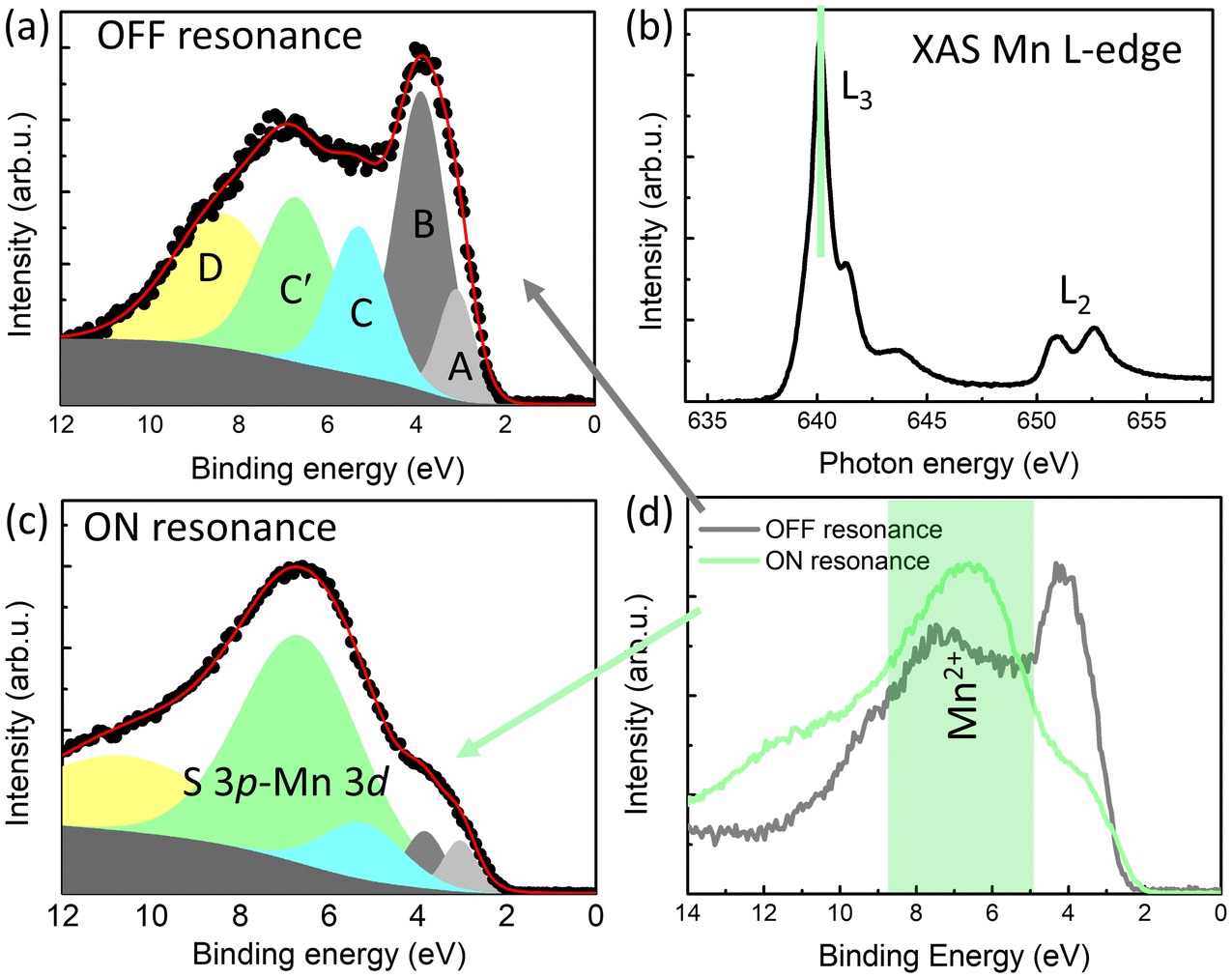 | ||
| Fig. 5 RESPES measurements for the Mn-MoS2 sample. (a) Off-resonance measurement at 630 eV excitation energy. (b) Mn L2,3-edge XAS spectra, the green line highlighting the maximum of the edge intensity to whose energy we perform the on-resonance measurement. (c) On-resonance measurement at 640 eV excitation energy. (d) Off- (black) and Mn On-resonance (green) measurements of the valence band. | ||
 | ||
| Fig. 6 RESPES measurements for the Co-MoS2 sample. (a) Off-resonance measurement at 769 eV excitation energy. (b) Mn L2,3-edge XAS spectra, the green line highlighting the maximum of the edge intensity to whose energy we perform the on-resonance measurement. (c) On-resonance measurement at 781 eV excitation energy. (d) Off- (black) and Co On-resonance (orange) measurements of the valence band. | ||
Since such Mo 4d bands are not affected by the Mn doping, the shift of the S 3p–Mo 4d hybridized C band can be considered mainly a consequence of the shift of the S 3p band closer to the Fermi level. Therefore, Mn doping enhances the H–S bonding strength and S atoms can be considered more effective active sites than Mo.12
With regard to the Co-MoS2 sample, in Fig. 6(d), the larger contribution from Co2+ is expected at about 5 eV according to literature results.45 The presence of a Co3+ contribution is expected above 7 eV. Similarly to the case of Mn-MoS2, the fit of the off and on resonance VB spectra reported in Fig. 6(a) and (c) was performed by adding a further contribution labelled as C′ in Fig. 6(a) to the VB of the undoped case in Fig. S15.† The C′ band corresponds to the Co 3d band, which is less hybridized with S 3p whose contribution begins to be relevant above 5 eV. Due to such Co 3d additional contribution, we can observe that the S 3p–Mo 4d hybridized C band is slightly shifted farther from the Fermi level. The Co and Mo metallic bands are closer to the Fermi level, but those of Mo do not move compared to the non-doping case. Then, we can assume that Co doping enhances the H–Co bonding strength and Co atoms can be considered as active sites.
These results are confirmed also in the case of thinner films (Fig. S16†), demonstrating the intrinsic origin of the shift of the valence band contributions. Therefore, our RESPES results demonstrate that the improved HER properties, which we observed upon Mn doping by electrochemical measurements, can be explained by the S 3p band shift towards the VB edge. In contrast, when the Co 3d band contribution is added in the VB fit, the hybridized S–Mo band shifts farther from the Fermi level, while it is the Co 3d band that is closer to it. As a consequence, the enhancement of H adsorption/desorption is less effective than in the case of Mn doping, as demonstrated by the electrochemical measurements, and it is mainly related to the electron transfer from the Co site.
Experimental
Thin film deposition and characterization
Doped and undoped 2H-MoS2 films were grown by PLD at the NFFA-APE facility of IOM-CNR and Elettra in Trieste using a KrF excimer pulsed laser source with a typical energy density of about 2 J cm−2 and the laser repetition rate was varied from 1 to 10 Hz. The films were grown under an ultra-pure Ar pressure (99.9999%). The background pressure was varied from high vacuum (i.e. base pressure in the range of 10−8 mbar) up to 10−1 mbar. The films were grown at 650 °C on a (111) NbSTO single crystal substrate. By using the conductive substrate, we can limit the sample charging during the spectroscopic measurements. Deposition parameters were optimized in order to get a very low deposition growth rate, which ultimately was set to about 324 laser shots per unit cell for MoS2, while 5 times slower for Mn and 20 times slower for Co. The growth rate was calibrated by reflectivity measurements and Raman spectroscopy. The undoped MoS2 sample was obtained by focusing the laser pulses on a stoichiometric polycrystalline MoS2 target (purity 99.99%). Mn (or Co) doping was obtained by alternating the laser beam on the MoS2 and Mn (or Co) metal targets. The calibration of the Mn (or Co) content was achieved by XPS measurements. In this work, the doping concentration is in the range of 5–6% for Mn and 5–7% for Co, as determined by XPS. The composition results reported in Fig. S14† are in agreement with Energy-Dispersive X-ray Spectroscopy (EDX) measurements. After the film growth, the samples were cooled down to room temperature at about 30 min under deposition pressure conditions and transferred in situ to the XPS analysis chamber through the distribution center chamber of the APE beamline.X-ray diffraction measurements were performed with a Malvern Panalytical Empyrean analytic diffractometer using a Cu Kα source. In particular, low-angle X-ray reflectivity measurements were performed with a point detector while theta–2theta scans were obtained by using a Galipix 2D detector.
The surface morphology was studied using a Zeiss Supra 40 field-emission gun (FEG) Scanning Electron Microscope (SEM) equipped with an Oxford X-Act silicon drift detector for EDX.
Raman measurements were performed using a Horiba LabRAM HR800 system coupled with an Olympus BX41 inverted optical microscope and using a laser source with an excitation wavelength of 532 nm. The laser power was adjusted to avoid sample damage or any sample modification, as observed by optical microscopy. Spectra were acquired between 300 and 500 cm−1 with 1 s exposure time and as an average of ten different measurements.
AFM topography and KPFM measurements were performed in contact mode with a Bruker Multimode 8 AFM using Pt/Ir-coated cantilevers (PPP-EFM Nanosensors). The samples (size = 0.5 × 0.5 cm2) were glued on metallic sample holder disks with conductive tape and then additionally connected to the sample holders with silver paste. WF values of the doped and undoped MoS2 samples were obtained from CPD images according to the following equation: WF(MoS2) = WF(tip) + e × CPD, where e it is the electronic charge and WF(tip) was extracted from the CPD images of a gold calibration sample, assuming WF(gold) = 5.1 V.
High-resolution TEM (HRTEM) investigations were carried out on cross-sectional samples using a JEOL 2010 UHR operated at 200 kV and equipped with a field emission gun with a determined spherical aberration coefficient Cs = 0.47 ± 0.01 mm. Combined Scanning TEM (STEM) and Energy Dispersive X-ray Spectroscopy (EDS) were used to address the chemical assessment by site-selective chemical profiles. TEM samples in cross-sectional geometry were prepared by conventional polishing, followed by dimpling and milling with Ar ions.
Electrochemical characterization
Electrochemical measurements were performed with a three-electrode system on an electrochemical workstation (BioLogic, SP-300) in a standard cell at room temperature in 0.5 M H2SO4 electrolyte, where the sample is the working electrode, Hg/HgCl2 (saturated KCl) is the reference electrode, and a graphite rod is the counter electrode. For the sample preparation as the working electrode, non-conductive epoxy is used as a waterproof layer, Ag glue as a binder and Ti wire as a conductor (Fig. S9†). The area of each electrode was accurately determined using image processing software and is reported in Table S1.†Polarization curves were recorded by linear sweep voltammetry with a scan rate of 10 mV s−1. The measured potentials relative to the reference electrode EHg/HgCl2 were converted with respect to RHE by the following equation:

 .
.
The Tafel plots [overpotential versus log(current density)] were fitted to get their slope by the Tafel equation: η = b × log![[thin space (1/6-em)]](https://www.rsc.org/images/entities/char_2009.gif) j + logj0, where η is the overpotential, j is the current density, j0 is the exchange current density and b is the Tafel slope.46
j + logj0, where η is the overpotential, j is the current density, j0 is the exchange current density and b is the Tafel slope.46
EIS measurements were performed in the frequency range from 200 kHz to 200 mHz at −0.24 V, −0.34 V, and −0.44 V.
CV measurements were performed at scan rates of 20, 50, 100, 200, and 500 mV s−1 in the range of 0.32–0.42 V. Such measurements can give information on the electrochemical surface area (ECSA), which is the actual area of the catalyst surface on which the electrochemical reaction of interest occurs.47 The stability tests were performed by CV measurements for 500 cycles.
Spectroscopic measurements
XPS and XAS measurements by synchrotron radiation were used to measure samples grown in situ by the PLD system directly connected to the transfer chamber of the APE-HE beamline at Elettra synchrotron in Trieste. The in situ transferring procedure limits the surface contaminants effects and guarantees that the samples were all measured under identical conditions, so that a reliable comparison of surface properties vs. doping concentration can be performed. XPS measurements were performed at room temperature using a hemispherical electrostatic analyzer with the sample at 45° with respect to the impinging linearly polarized light and normal to the surface. The binding energies of the photoemission peaks were calibrated with respect to the Fermi level of Au reference samples. XAS measurements were performed on the same geometry in total electron yield mode at room temperature, normalizing the intensity of the sample current to the incident photon flux measured on a grid placed between the last mirror and the analysis chamber.The occupied electronic states in the valence band have been studied by RESPES with photon energies across the Mn and Co absorption L-edges (2p → 3d) and the Mo M-edge (3p → 4d). In the off-resonant photoemission process, only the direct process of electron excitation occurs from a valence state into the continuum following absorption of a photon. In resonance, a new transition channel opens up, namely when the photon energy is around the absorption threshold, in the case of 3d transition metal atoms such as cobalt and manganese, the incoming photon excites a 2p electron to an empty 3d level and in the case of molybdenum, the electron is excited from the 3p to the empty 4d level. This core-excitation process is followed by the decay of the core-excited state through auto-ionization. In the latter process, the excited electron and one valence electron scatter by Coulomb interaction such that one electron fills the core-hole and the other one is ejected as the photoelectron. In resonant photoemission, the core-excitation and auto-ionization have to be considered as a coherent process yielding a final state identical to that obtained by the direct photoemission process.
Conclusions
We studied the Mn and Co doping effects in MoS2 thin films grown by PLD for HER. The two dopant cations are respectively on the left and on the right of the volcano curve of the exchange current as a function of the adsorption free energy of H atoms reported in the literature.13 The electrochemical measurements show a better HER activity in the order of MoS2 < Co-MoS2 < Mn-MoS2. Core level shifts and VB measurements in XPS show that the electronic properties are modified by doping. More intriguing results are obtained from RESPES measurements, which allow to get in a direct manner the involvement of the Mn and Co bands in the VB spectra. Having identified such contributions, an analysis of the VB was carried out as the dopant varies, showing a shift of the S–Mo hybridized band closer to the Fermi level in the case of Mn-MoS2 and farther to it in the case of Co-MoS2.Our results demonstrate that in the case of Mn doping, the active sites are mainly S ions, while in the case of Co doping, the role of Co ions as active sites becomes relevant. These findings are in agreement with the electrochemical measurements. The HER improvement in the case of Co doping in MoS2 with respect to the undoped film is mainly related to the electron exchange of H with Co ions acting as main active sites. In contrast, the lower potential needed to start the HER process and to reach an operating current density demonstrates that the sulfur ions as active sites induced by Mn doping are more effective, in agreement with the even better HER properties of Mn-MoS2 with respect to Co-MoS2 and undoped MoS2.
We therefore elucidate the role of the dopant cation in the electronic structure determining the active site for H adsorption/desorption, which can be extremely useful for designing efficient materials for hydrogen production via the doping pathway. From the point of view of the electronic properties, the behavior of the VB contributions with different doping concentrations in MoS2 can also be useful in other fields of materials science, as the field of magnonics, where our results can be relevant for dilute magnetic semiconductor engineering.48 In addition, we demonstrate the doping effect on vacancy-induced electronic states within the gap. This finding is fundamental for properly tuning the wavelength range for the optical absorption of MoS2-based photo-devices.
Author contributions
P. Orgiani: conceptualization, formal analysis, investigation, supervision, and writing – review and editing. L. Braglia, V. Polewczyk, and Z. Nie: formal analysis, investigation, and writing – review and editing. F. Lavini, S. P. Chalil, S. K. Chaluvadi, P. Rajak, E. Dobovičnik, and F. Morabito: investigation. V. Foglietti: conceptualization and writing – review and editing. P. Torelli, E. Riedo, R. Ciancio, and N. Yang: conceptualization, supervision, and writing – review and editing. C. Aruta: conceptualization, formal analysis, funding acquisition, investigation, project administration, supervision, writing – original draft, and writing – review and editing.Conflicts of interest
There are no conflicts to declare.Acknowledgements
This work has been partially performed in the framework of the Nanoscience Foundry and Fine Analysis (NFFA-MIUR Italy Progetti Internazionali) facility in Trieste, Italy, proposal no. NFFA-TS 2016-009 and 2020-001. We acknowledge the support from the Italian Ministry of Research under the PRIN 2022 Grant No. 202228P42F with title “Transition metal dichalcogenide thin films for hydrogen generation” PE3 funded by PNRR Mission 4 Istruzione e Ricerca – Componente C2 – Investimento 1.1, Fondo per il Programma Nazionale di Ricerca e Progetti di Rilevante Interesse Nazionale PRIN 2022 – CUP B53D23003800006. Research at SPIN-CNR was supported by the project ECS00000024 “Ecosistemi dell'Innovazione”—Rome Technopole of the Italian Ministry of University and Research, public call no. 3277, PNRR—Mission 4, Component 2, Investment 1.5, financed by the European Union, Next Generation EU.Notes and references
- Z. W. Seh, J. Kibsgaard, C. F. Dickens, I. Chorkendorff, J. K. Nørskov and T. F. Jaramillo, Science, 2017, 355, 146 CrossRef PubMed.
- D. Voiry, J. Yang and M. Chhowalla, Adv. Mater., 2016, 28, 6197 CrossRef CAS PubMed.
- J. Hou, X. Peng, J. Sun, S. Zhang, Q. Liu, X. Wang, J. Luo and X. Liu, Inorg. Chem. Front., 2022, 9, 3047 RSC.
- H. Wei, J. Si, L. Zeng, S. Lyu, Z. Zhang, Y. Suo and Y. Hou, Chin. Chem. Lett., 2023, 34, 107144 CrossRef CAS.
- X. Liu, Y. Hou, M. Tang and L. Wang, Chin. Chem. Lett., 2023, 34, 107489 CrossRef CAS.
- M. Samadi, N. Sarikhani, M. Zirak, H. Zhang, H.-L. Zhang and A. Z. Moshfegh, Nanoscale Horiz., 2018, 3, 90 RSC.
- J. D. Benck, T. R. Hellstern, J. Kibsgaard, P. Chakthranont and T. F. Jaramillo, ACS Catal., 2014, 4, 3957 CrossRef CAS.
- X. Hu, Q. Zhang and S. Yu, Appl. Surf. Sci., 2019, 478, 857 CrossRef CAS.
- J. H. Lee, W. S. Jang, S. W. Han and H. K. Baik, Langmuir, 2014, 30, 9866 CrossRef CAS PubMed.
- N. Markovic, B. Grgur and P. J. Ross, J. Phys. Chem. B, 1997, 101, 5405 CrossRef CAS.
- Y. Cao, ACS Nano, 2021, 15, 11014 CrossRef CAS PubMed.
- J. Deng, H. Li, S. Wang, D. Ding, M. Chen, C. Liu, Z. Tian, K. S. Novoselov, C. Ma, D. Deng and X. Bao, Nat. Commun., 2017, 8, 14430 CrossRef CAS PubMed.
- J. Deng, H. Li, J. Xiao, Y. Tu, D. Deng, H. Yang, H. Tian, J. Li, P. Ren and X. Bao, Energy Environ. Sci., 2015, 8, 1594 RSC.
- Y. Huang, R. J. Nielsen, W. A. Goddard and M. P. Soriaga, J. Am. Chem. Soc., 2015, 137, 6692 CrossRef CAS PubMed.
- J. Staszak-Jirkovský, C. D. Malliakas, P. P. Lopes, N. Danilovic, S. S. Kota, K.-C. Chang, B. Genorio, D. Strmcnik, V. R. Stamenkovic, M. G. Kanatzidis and N. M. Markovic, Nat. Mater., 2016, 15, 197 CrossRef PubMed.
- R. Wang, P. Sun, H. Wang and X. Wang, Electrochim. Acta, 2017, 258, 876 CrossRef CAS.
- P. Orgiani, S. K. Chaluvadi, S. P. Chalil, F. Mazzola, A. Jana, S. Dolabella, P. Rajak, M. Ferrara, D. Benedetti, A. Fondacaro, F. Salvador, R. Ciancio, J. Fujii, G. Panaccione, I. Vobornik and G. Rossi, Rev. Sci. Instrum., 2023, 94, 033903 CrossRef CAS PubMed.
- S.-L. Li, H. Miyazaki, H. Song, H. Kuramochi, S. Nakaharai and K. Tsukagoshi, ACS Nano, 2012, 6(8), 7381 CrossRef PubMed.
- C. Lee, H. Yan, L. E. Brus, T. F. Heinz, J. Hone and S. Ryu, ACS Nano, 2010, 4, 2695 CrossRef CAS PubMed.
- Y. Yu, C. Li, Y. Liu, L. Su, Y. Zhang and L. Cao, Sci. Rep., 2013, 3, 1866 CrossRef PubMed.
- J. C. Wildervanck and F. Jellinek, Z. Anorg. Allg. Chem., 1964, 328, 309 CrossRef CAS.
- C. Kisielowski, Q. M. Ramasse, L. P. Hansen, M. Brorson, A. Carlsson, A. M. Molenbroek, H. Topsøe and S. Helveg, Angew. Chem., Int. Ed., 2010, 49, 2708 CrossRef CAS PubMed.
- F. Lavini, A. Calò, Y. Gao, E. Albisetti, T.-D. Li, T. Cao, G. Li, L. Cao, C. Aruta and E. Riedo, Nanoscale, 2018, 10, 8304 RSC.
- J. Kibsgaard and I. Chorkendorff, Nat. Energy, 2019, 4, 430 CrossRef.
- T. Shinagawa, A. T. Garcia-Esparza and K. Takanabe, Sci. Rep., 2015, 5, 13801 CrossRef PubMed.
- A. P. Murthy, J. Theerthagiri and J. Madhavan, J. Phys. Chem. C, 2018, 122, 23943 CrossRef CAS.
- S. Wang, J. Zhang, O. Gharbi, V. Vivier, M. Gao and M. E. Orazem, Nat. Rev. Methods Primers, 2021, 1, 41 CrossRef CAS.
- Y.-H. Choi, J. Lee, A. Parija, J. Cho, S. V. Verkhoturov, M. Al-Hashimi, L. Fang and S. Banerjee, ACS Catal., 2016, 6, 6246 CrossRef CAS.
- S. Shin, Z. Jin, D. H. Kwon, R. Bose and Y.-S. Min, Langmuir, 2015, 31, 1196 CrossRef CAS PubMed.
- D. Voiry, M. Chhowalla, Y. Gogotsi, N. A. Kotov, Y. Li, R. M. Penner, R. E. Schaak and P. S. Weiss, ACS Nano, 2018, 12, 9635 CrossRef CAS PubMed.
- Z. Cai, M. Kubicek, J. Fleig and B. Yildiz, Chem. Mater., 2012, 24, 1116 CrossRef CAS.
- L. Dahéron, R. Dedryvère, H. Martinez, M. Ménétrier, C. Denage, C. Delmas and D. Gonbeau, Chem. Mater., 2008, 20, 583 CrossRef.
- M. A. van Veenendaal and G. A. Sawatzky, Phys. Rev. Lett., 1993, 70, 2459 CrossRef CAS PubMed.
- L. A. H. Jones, Z. Xing, J. E. N. Swallow, H. Shiel, T. J. Featherstone, M. J. Smiles, N. Fleck, P. K. Thakur, T.-L. Lee, L. J. Hardwick, D. O. Scanlon, A. Regoutz, T. D. Veal and V. R. Dhanak, J. Phys. Chem. C, 2022, 126, 21022 CrossRef CAS PubMed.
- J. Kopaczek, S. J. Zelewski, M. P. Polak;, A. Gawlik, D. Chiappe, A. Schulze, M. Caymax and R. Kudrawiec, J. Appl. Phys., 2019, 125, 135701 CrossRef.
- L. H. Tjeng, C. T. Chen, J. Ghijsen, P. Rudolf and F. Sette, Phys. Rev. Lett., 1991, 67, 501 CrossRef CAS PubMed.
- G. van der Laan, B. T. Thole, H. Ogasawara, Y. Seino and A. Kotani, Phys. Rev. B: Condens. Matter Mater. Phys., 1992, 46, 7221 CrossRef CAS PubMed.
- V. Carozo, Y. Wang, K. Fujisawa, B. R. Carvalho, A. McCreary, S. Feng, Z. Lin, C. Zhou, N. Perea-López, A. L. Elías, B. Kabius, V. H. Crespi and M. Terrones, Sci. Adv., 2017, 3, e1602813 CrossRef PubMed.
- Y. Zhaoa, M. T. Tang, S. Wu, J. Geng, Z. Hand, K. Chan, P. Gao and H. Li, J. Catal., 2020, 382, 320 CrossRef.
- B. Gobaut, P. Orgiani, A. Sambri, E. di Gennaro, C. Aruta, F. Borgatti, V. Lollobrigida, D. Céolin, J.-P. Rueff, R. Ciancio, C. Bigi, P. Kumar Das, J. Fujii, D. Krizmancic, P. Torelli, I. Vobornik, G. Rossi, F. Miletto Granozio, U. Scotti di Uccio and G. Panaccione, ACS Appl. Mater. Interfaces, 2017, 9, 23099 CrossRef CAS PubMed.
- B. Gilbert, B. H. Frazer, A. Belz, P. G. Conrad, K. H. Nealson, D. Haskel, J. C. Lang, G. Srajer and G. De Stasio, J. Phys. Chem. A, 2003, 107, 2839 CrossRef CAS.
- C.-J. Chen, P.-T. Chen, M. Basu, K.-C. Yang, Y.-R. Lu, C.-L. Dong, C.-G. Ma, C.-C. Shen, S.-F. Hu and R.-S. Liu, J. Mater. Chem. A, 2015, 3, 23466 RSC.
- N. Kornienko, J. Resasco, N. Becknell, C.-M. Jiang, Y.-S. Liu, K. Nie, X. Sun, J. Guo, S. R. Leone and P. Yang, J. Am. Chem. Soc., 2015, 137, 7448 CrossRef CAS PubMed.
- L. Sangaletti, S. Pagliara, F. Parmigiani, A. Goldon, L. Floreano, A. Morgante and V. Aguekian, J. Electron Spectrosc. Relat. Phenom., 2004, 137, 553 CrossRef.
- Y. Lykhach, S. Piccinin, T. Skála, M. Bertram, N. Tsud, O. Brummel, M. Farnesi Camellone, K. Beranová, A. Neitzel, S. Fabris, K. C. Prince, V. Matolín and J. Libuda, J. Phys. Chem. Lett., 2019, 10, 6129 CrossRef CAS PubMed.
- Y. Yu, S.-Y. Huang, Y. Li, S. N. Steinmann, W. Yang and L. Cao, Nano Lett., 2014, 14, 553 CrossRef CAS PubMed.
- P. Connor, J. Schuch, B. Kaiser and W. Jaegermann, Z. Phys. Chem., 2020, 234, 979 CrossRef CAS.
- A. Ramasubramaniam and D. Naveh, Phys. Rev. B: Condens. Matter Mater. Phys., 2013, 87, 195201 CrossRef.
Footnote |
| † Electronic supplementary information (ESI) available: Raman spectroscopy; high-resolution transmission electron microscopy; Kelvin probe force microscopy; electrochemical characterization; X-ray photoemission spectroscopy; valence band fit. See DOI: https://doi.org/10.1039/d4nr00876f |
| This journal is © The Royal Society of Chemistry 2024 |