
 Open Access Article
 This Open Access Article is licensed under a
 Creative Commons Attribution 3.0 Unported Licence
Imaging of ultrafast photoexcited electron dynamics in pentacene nanocrystals on a graphite substrate†
Masahiro
Shibuta‡
 a and
Atsushi
Nakajima
*ab
a and
Atsushi
Nakajima
*ab
aKeio Institute of Pure and Applied Sciences (KiPAS), Keio University, 3-14-1 Hiyoshi, Kohoku-ku, Yokohama 223-8522, Japan. E-mail: nakajima@chem.keio.ac.jp
bDepartment of Chemistry, Faculty of Science and Technology, Keio University, 3-14-1 Hiyoshi, Kohoku-ku, Yokohama 223-8522, Japan
First published on 21st May 2024
Abstract
Understanding molecular film growth on substrates and the ultrafast electron dynamics at their interface is crucial for advancing next-generation organic electronics. We have focused on studying the ultrafast photoexcited electron dynamics in nanoscale organic crystals of an aromatic molecule, pentacene, on a two-dimensional material of graphite substrate. Through the use of time-resolved two-photon photoelectron emission microscopy (2P-PEEM), we have visualized the ultrafast lateral evolution of photoexcited electrons. By resonantly tuning the incident photon to excite pentacene molecules, polarization-dependent 2P-PEEM has revealed that pentacene nanocrystals (sub- to several μm) on the substrate exhibit a preferential orientation, in which a molecular π-orbital contacts the substrate in a “lying flat” orientation, facilitating electron transfer to the substrate. The time-resolved 2P-PEEM captures the motion of excited electrons in a femto- to pico-second timescale, clearly imaging the ultrafast charge transfer and lateral expansion two-dimensionally on the graphite substrate. Moreover, we found that the lying-flat molecular orientation of pentacene nanocrystals is transformable into a “standing-up” one through gentle heating up to 50 °C. These experimental insights using time-resolved 2P-PEEM will be highly valuable in enhancing the photofunctionalities of organic electronic devices by controlled molecular deposition.
Introduction
Organic electronics represent one of the most significant technological advancements of the early 21st century, providing the ability to create low-cost, lightweight, and flexible electronic components, such as electroluminescent devices, solar cells, and field-effect transistors. Although thin films of π-conjugated organic molecules serve as the basis for these devices, their performance is limited because of the inherently inhomogeneous growth of organic crystals on the substrate surface, resulting in sub- to several micron-sized nanocrystal domains, which is in contrast to inorganic semiconductors that are well-controlled by epitaxial crystallization coupled with lattice matching.1In general, the performance of organic devices is governed by ultrafast carrier dynamics within organic films and at the organic–substrate interface, which are significantly influenced by the inhomogeneous growth of organic crystals on a substrate. The crystallinity and crystal axis of organic aggregates attached to substrates (electrodes) strongly affect the injection/ejection and separation properties of photogenerated active carriers at the interface.2–7 Therefore, to advance organic electronics in the next generation, it is necessary to develop a methodology capable of simultaneously elucidating both the crystal growth of organic molecules on substrates and ultrafast carrier dynamics in such an inhomogeneous system.
Recent efforts have focused on microscopically investigating the crystal growth of organic molecules deposited on substrates, in which the substrate properties, deposition temperature, and flux are the key parameters that greatly influence the growth mode.8–14 Meanwhile, for the ultrafast carrier dynamics of organic crystals on the substrate, spectroscopic characterizations of electronic states have been performed using ultrafast light sources.15,16 To fully understand and optimize device functionality, it is imperative that these microscopic and spectroscopic characterizations should be conducted simultaneously.
For the microscopic characterizations of organic crystals grown on substrates, ultraviolet or X-ray spectroscopy combined with nanoscale focusing can simultaneously characterize the orientation of organic nanocrystals and electronic states.17–19 Scanning tunneling microscopy/spectroscopy (STM/STS) can be used to resolve the growth of organic molecules with an atomic resolution and point-by-point electronic structure.20–24 Photoelectron emission microscopy (PEEM) is another promising experimental approach that directly images the lateral distribution of photoemission with a spatial resolution of a few tens of nm.2,25–30 It is worth noting that the latest PEEM apparatus can achieve energy and momentum resolutions as a “momentum microscopy” or “orbital tomography”, which enables local photoelectron spectroscopy on a single organic crystal domain.23,31,32
To access ultrafast dynamics of organic crystals and crystal–substrate interfaces in energetic and spatial dimensions, the aforementioned experimental approaches should be combined with a femtosecond light source. Among these methods, the PEEM-based experiment stands out as an efficient and straightforward method, in which a femtosecond pulse laser electronically excites an organic system, and another pulse subsequently extracts the excited electrons (or excitons) as photoelectrons (i.e., two-photon (2P-) PEEM).33–46
In this study, we investigated the nanoscale morphology of pentacene nanocrystals on a highly oriented pyrolytic graphite (HOPG) substrate and their ultrafast electronic behavior at the crystal-substrate interface using time-resolved 2P-PEEM. Pentacene is a well-known polycyclic aromatic carbon used as an electron-donating (p-type) organic semiconductor, while HOPG is an electron-conducting material, also with graphene-like properties. By taking advantage of a linearly polarized laser photon that resonantly excites the pentacene molecule, the 2P-PEEM intensity contrast provides a sensitive visualization of the crystal orientation, similar to polarized microscopy but with better lateral resolution (<80 nm). Our polarization-dependent 2P-PEEM image reveals pentacene nanocrystals with a “lying-flat” molecular arrangement on the substrate, where the molecular π-orbitals are facing the substrate, promoting efficient photoinduced electron donation. By employing time-resolved 2P-PEEM, electron transfer from the pentacene nanocrystals into the HOPG substrate is captured on a femto- to pico-second timescale, elucidating: (1) the injection of photoexcited electrons from the nanocrystals into the HOPG substrate, and (2) the injected electron expands two-dimensionally by approximately 340 nm during its energy loss.
Furthermore, we demonstrate a transformation of pentacene nanocrystals to a “standing-up” orientation with a gentle heating treatment (50 °C for 10 min), highlighting the interplay between differing results from previous studies on the pentacene/HOPG system.22,47–50
Results
Growth of pentacene nanocrystals on HOPG
Fig. 1a and b show the 2P-PEEM images captured with a photon energy (hν) of 4.33 eV for pentacene films on a HOPG substrate at different deposition times of (a) 2 min and (b) 28 min, respectively. A planar image exhibiting a vague contrast is obtained at 2 min deposition. At this deposition time, a fully covered pentacene molecular film is formed, which is spectroscopically characterized by detecting 2P-ptotoelectrons (i.e., 2P-PES).51–57Fig. 1c shows the 2P-PES spectra for the same samples after a series of 2P-PEEM measurements; an electron energy analyzer is integrated in the same ultrahigh vacuum system.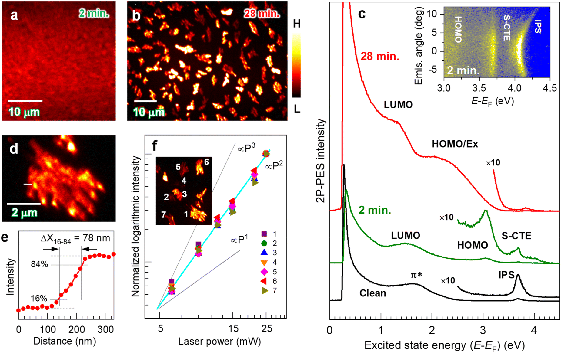 | ||
| Fig. 1 (a and b) 2P-PEEM images (hv = 4.33 eV, p-pol.) of pentacene films deposited on a HOPG substrate, where the deposition times are (a) 2 min and (b) 28 min, respectively (see Fig. 2c for the polarization configuration). The contrast of each image was appropriately adjusted for visual perception. (c) The corresponding 2P-PES spectra to (a) and (b), where the horizontal axis stands for excited state energy with respect to the Fermi level (EF). By depositing pentacene for 2 min (middle), the LUMO (EF + 1.5 eV) and HOMO (EF − 1.2 eV) are resolved. IPS and S-CTE are also resolved, exhibiting free-electron-like dispersive and nondispersive characteristics, respectively (see inset for angle-resolved 2P-PES with hν = 4.77 eV). In the 2P-PEEM image at 28 min deposition in (b), island structures exhibit intensity variations. The 2P-PES intensity (top in (c)) is enhanced due to effective photoexcitation at the pentacene nanocrystal, revealing that the exciton-derived peak merged with the HOMO-derived one (HOMO/Ex) in addition to LUMO. Detailed peak assignments on both deposited samples are shown in Text S1 and Fig. S1 and S3 in the ESI.† (d) 2P-PEEM image magnified at an island domain formed by 28 min deposition. (e) Intensity profile along a white line in (d). The lateral resolution (width of 16–84 intensity, ΔX16–84) is evaluated to be 78 nm. (f) 2P-PEEM intensities at selected nanocrystals as a function of the incident laser power (P), which are normalized to those obtained with the highest laser power (P = 25 mW). P2 dependence in all nanocrystals confirms that the PEEM technique images the photoemission with a 2P-process, such as 2P-PEEM. | ||
At 2 min deposition, both the highest occupied and lowest unoccupied molecular orbitals (HOMO and LUMO) consisting of π-orbitals appear as frontier molecular orbitals at −1.2 eV and +1.5 eV with respect to the Fermi level (EF), respectively (see Text S1 and Fig. S1 in the ESI† for detailed peak assignments). The LUMO energy position corresponds to the value obtained by a STM.58 A sharp spectral profile of the HOMO-derived peak is similar to that obtained by ultraviolet photoelectron spectroscopy (UPS) for a first wetting layer of pentacene film on the HOPG substrate in a Stranski–Krastanov (S–K) growth mode,59,60 in which the frontier π-orbitals of pentacene are in contact with the substrate (see also Fig. S2 in the ESI† for UPS data of the corresponding sample). Furthermore, an image potential state (IPS)53,57,61,62 and a state of surface charge transfer exciton (S-CTE)62–64 are resolved, as shown in the inset in Fig. 1c for an angle-resolved 2P-PES; the former exhibits free electron-like angular dispersion, while the latter is less dispersive, both confirming the uniform formation of 1 monolayer (ML) pentacene on HOPG. It should be noted that the IPS of the clean HOPG substrate (bottom in Fig. 1c) disappears after 2 min deposition, indicating that the 2 min deposition of pentacene corresponds to 1 ML coverage. These microscopic and spectroscopic measurements indicate that pentacene molecules in the uniform 1 ML film lie flat on a HOPG substrate as a wetting layer.
On the other hand, inhomogeneous island structures cover the entire surface at a higher deposition amount (28 min) (Fig. 1b, see also Fig. S3 (ESI†) for a wider field of view). These islands have domain sizes ranging up to several μm.2 A magnified image of the observed island (Fig. 1d) shows the growth of the pentacene nanocrystal on the substrate, in which the lateral resolution of the present 2P-PEEM is evaluated to be 78 nm from an intensity histogram at a crystal boundary (Fig. 1e). The 2P-PES spectrum for the corresponding sample (Fig. 1c top) consistently indicates the molecular crystallization on a wetting substrate known as the S–K growth mode. The LUMO-derived peak broadens and shifts toward lower energy by 0.2 eV (EF + 1.3 eV) because of an intermolecular interaction promoted by π-stacked pentacene molecules. Another broad structure labeled “HOMO/Ex” is assignable to a combination of broadened HOMO14,48,65,66 and exciton-derived features (see Text S1 and Fig. S4 in the ESI† for detailed assignments). Furthermore, intense signals are detected near the low-energy cutoff, in which the excited electrons possessing energy higher than 0.2 eV with respect to the EF are detected in the present 2P-PES and 2P-PEEM experiments. It should be noted that the validity of the comparative discussion can be confirmed between the microscopic (2P-PEEM) and spectroscopic (2P-PES) observations. Fig. 1f plots the PEEM intensities of selected nanocrystals (see inset) versus incident laser powers (P), showing the exact square dependence (∝P2) because of the 2P-photoemission process as 2P-PEEM.
In the 2P-PEEM for pentacene nanocrystals (28 min, Fig. 1b), there are notable intensity variations, which are caused by an anisotropy of the pentacene nanocrystals grown on the HOPG substrate. When the polarization of the excitation light is changed, the 2P-PEEM can sensitively characterize the crystal orientation. Fig. 2a and b compare the 2P-PEEM image of pentacene nanocrystals excited with s- and p-polarized photons, respectively. The directions of light polarization projected on the surface plane are indicated at the upper left of each figure, while the polarization configuration is schematically illustrated in Fig. 2c. The 2P-PEEM intensities at each pentacene nanocrystal vary upon rotation of the polarization directions (angle of electric field, θ = 0° represents s-polarization, while θ = 90° indicates p-polarization).
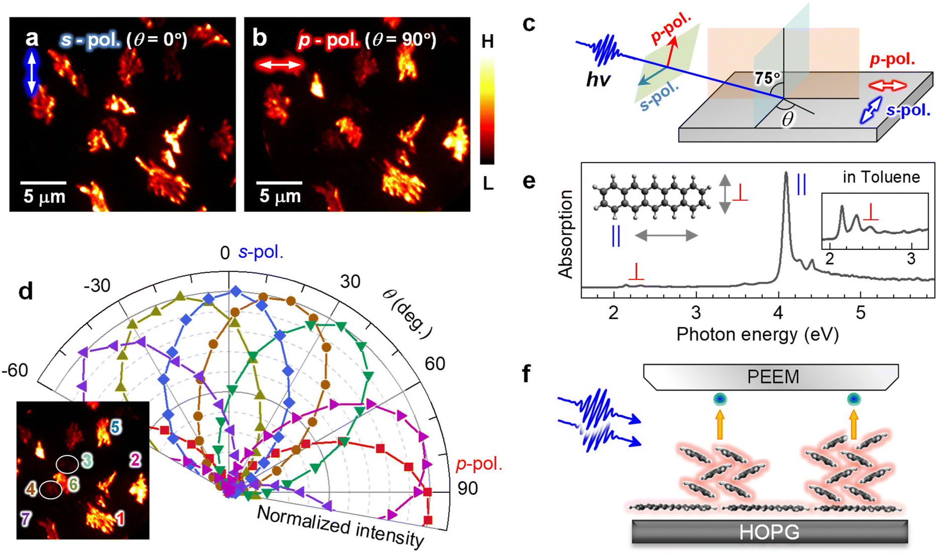 | ||
| Fig. 2 (a and b) 2P-PEEM pentacene deposited (28 min) on a HOPG substrate taken with (a) s- and (b) p-polarized photons (hv = 4.33 eV). Light polarizations projected on the surface are indicated by white arrows in the upper left of each figure. (c) Light polarization configuration. (d) Polar plots of normalized 2P-PEEM intensities at selected nanocrystals. The inset shows the selection of seven nanocrystals in the 2P-PEEM image. The intensities are randomly maximized at a certain θmax with sin2(θ − θmax) dependence. (e) Absorption spectrum of pentacene in toluene solution. The strong absorption peak originates from the effective molecular excitation with a polarized light along the long molecular axis (denoted as “∥”), while the peak at the lowest energy is due to the photo absorption with a light polarized along the short molecular axis (denoted as “⊥”).67 (f) Schematic illustration of the crystal orientation at the initial growth of pentacene, where the pentacene nanocrystals actually consist of ≈50 molecular layers on average at 28 min deposition. | ||
Since the transition dipole moment of a molecule aligns with the specific molecular axis, the polarization retention dependence will provide information on the molecular orientation in the nanocrystals. Fig. 2d shows polar plots that illustrate the normalized 2P-PEEM intensities at selected nanocrystals, with the selection of seven nanocrystals shown in the inset. By changing the polarization angle of θ, the 2P-PEEM intensity of each nanocrystal exhibits a sin2![[thin space (1/6-em)]](https://www.rsc.org/images/entities/char_2009.gif) θ dependence, with the maximum intensity achieved at varying angles θ. As discussed below, the results indicate that all pentacene molecules in the nanocrystals align with their long molecular axis oriented parallel to the surface. Raw 2P-PEEM images captured with continuously rotating θ are shown in Movie S1 in the ESI.†
θ dependence, with the maximum intensity achieved at varying angles θ. As discussed below, the results indicate that all pentacene molecules in the nanocrystals align with their long molecular axis oriented parallel to the surface. Raw 2P-PEEM images captured with continuously rotating θ are shown in Movie S1 in the ESI.†
Here, the orientation of the pentacene nanocrystals is characterized in terms of the polarization-dependent 2P-PEEM. In this 2P-PEEM experiment, a specific resonance of a pentacene molecule is photoexcited by hν = 4.33 eV photons, resulting in an effective 2P-photoemission from the nanocrystals rather than the substrate. In fact, an optical absorption spectrum for the pentacene solution (Fig. 2e) shows a strong peak at the corresponding hν above 4 eV, at which the intensity is much higher than the first absorption peak (S1 state) at 2.15 eV.
According to theoretical calculations67 and optical spectroscopy for isolated pentacene molecules (e.g., embedded in a rare gas matrix68,69), the strong absorption band originates from the molecular excitation of HOMO → LUMO + 2 that has a high transition dipole moment, along with a long molecular axis of pentacene (see inset in Fig. 2e). In terms of the deposited arrangement of pentacene molecules, the differential reflection spectrum for a pentacene/Al2O3 system shows a strong signal at hν = 4.3 eV.70 The polarization-dependent 2P-PEEM results indicate that the pentacene nanocrystals are initially formed on the HOPG substrate with a lying-flat orientation, whose azimuth angles of the molecular axis are independent of the surface atomic orientation. The lying-flat orientation of pentacene molecules is schematically illustrated in Fig. 2f. Since the nanocrystals occupy approximately 25% of the surface area at 28 min deposition (14 ML equivalent including the wetting layer), the nanocrystals can consist of ≈50 layers of pentacene molecules on average.
It should be emphasized that orientation-sensitive 2P-PEEM, like a polarized optical microscopy, is realized by tuning the incident hν to selectively photoexcite pentacene molecules at a specific molecular axis, while having much better lateral resolution (ΔX16–84 = 78 nm) than optical imaging (typically 400–700 nm). In contrast to the present 2P-PEEM shown in Fig. 2, in fact, the nanocrystals show fewer intensity variations in the PEEM images when the PEEM measurements are performed with non-resonant hνs (see ESI, Fig. S5† for 2P-PEEM with hν = 2.88 eV and Fig. S6† for one-photon PEEM with hν = 5.97 eV).
Time-resolved 2P-PEEM: electron transfer into the substrate
A time-resolved 2P-PEEM with pump-probe optical configuration can directly access the lateral expansion of the photoexcited states in the electron-donating (p-type) pentacene nanocrystals. Fig. 3a shows the raw 2P-PEEM image of the pentacene nanocrystals at a pump-probe delay time (Δt) of 13 ps, where a single-colored pulse pair (hv = 4.33 eV, p-polarized) is generated by a set of beam splitters and combiner (see Fig. S7 in the ESI†). Randomly oriented pentacene nanocrystals with “lying flat” orientation exhibit intensity variations that are dependent on the crystal orientation, while the average size is much smaller than that seen in Fig. 1b and 2 because of the shorter deposition time (14 min). Since detectable intensity change is hardly observed in the raw data at Δt > 5 ps, the 2P-PEEM image at Δt = 13 ps (Fig. 3a, see also Fig. 3d for magnified image) can be regarded as a background signal in the series of time-resolved 2P-PEEM experiments. It should be noted that the background 2P-PEEM intensity originates from the 2P-photoemission emitted by the delayed pulses themselves.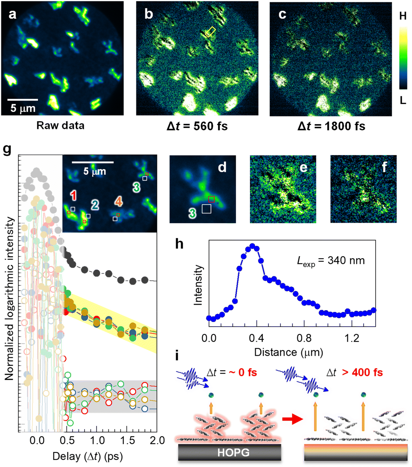 | ||
| Fig. 3 (a–c) Time-resolved 2P-PEEM (hv = 4.33 eV, p-polarization) for the pentacene nanocrystals on HOPG (14 min deposition); (a) A raw image at Δt = 13 ps for subtraction. (b and c) Subtracted 2P-PEEM images at (b) Δt = 560 fs and (c) Δt = 1800 fs. The intensity color scale is different among the 2P-PEEM images to appropriately visualize the experimental behavior in the time-resolved measurement; namely, photoexcited electrons at the substrate donated by pentacene nanocrystals are imaged, where signals “near” the nanocrystals are enhanced by the subtraction. (d–f) The magnified 2P-PEEM images at a nanocrystal correspond to (a), (b), and (c), respectively. (g) Integrated intensity traces against the delay time (Δt) at four nanocrystal domains (300 × 300 nm2) and their peripheries (500 × 500 nm2) (see inset for area selection as numbered from 1 to 4). The 2P-PEEM intensities at the peripheries of their nanocrystals exhibit exponential decay with a time constant of 3000 fs, while no detectable decay is observed at the nanocrystal cores. It should be noted that the intensity fluctuations at Δt < 0.4 ps (slightly smeared area) occur due to interference between two pulses within their overlapping time. The intensity traces at other different area sets (nanocrystal and its periphery) are shown in Fig. S8 (ESI†). The topmost profile (solid black circles) in (g) is for the entire 2P-PEEM intensity in the field of view, seemingly showing an average of the data at selected areas of both core and periphery regions. (h) Intensity profile of 2P-PEEM at Δt = 560 fs (marked in b). The expansion length, Lexp, is evaluated to be 340 nm. (i) Schematic illustration of the excited electron expansion after selective excitation at the pentacene nanocrystals. | ||
Fig. 3b and c show the background-subtracted 2P-PEEM images at Δt = 560 fs and 1800 fs, respectively. Compared with the background data (Fig. 3a or d), the 2P-PEEM signals exhibit lower intensity at each pentacene nanocrystal, but are stronger in the vicinity of the nanocrystals extending a few μm from the domain edge. In fact, as shown in the magnified images of Fig. 3d, e, and f, the initial bright nanocrystal core in Fig. 3d darkens over time, while a contrasting phenomenon is observed where the peripheries of the nanocrystals become brighter. The result indicates that the photoexcited electrons in the pentacene nanocrystals with lying-flat molecular orientation are rapidly transferred from the π-orbitals to the substrate, and expand two-dimensionally into the periphery of the nanocrystals (see Fig. 3i). The subtracted data at Δt = 520–7800 fs are illustrated in Movie S2 in the ESI.†
For a more quantitative discussion, in Fig. 3g, integrated intensity traces are evaluated against Δt at four sets of nanocrystal cores (open square; 300 × 300 nm2) and their peripheries (solid square; 500 × 500 nm2) (see inset for area selections and the corresponding numbers). The intensities around Δt = 0 fs fluctuate because of photon interference between the pump and probe photons. While the carefully measured fringe signal in the interferometric measurement provides important insights into the physical properties of the targeted system,51 our primary focus in this study is on elucidating the dynamics occurring from several 100 fs to ps after photoexcitation, revealing the temporal expansion of excited electrons in real space.
At Δt > 400 fs, the 2P-PEEM intensities at the peripheries of the nanocrystals (middle datasets with solid circles) exhibit a very similar exponential decay with a time constant of 3000 fs, whereas no detectable decay is observed at the nanocrystal cores (bottom datasets with open circles). All datasets analyzed for the other four regions (8 datasets = 16 regions) are shown in Fig. S8 (ESI†). Importantly, in the present study, the ultrafast excited electron dynamics could be successfully elucidated microscopically by selecting several 100 nm square sized-regions within a 20 μm square field of view. In fact, the entire 2P-PEEM intensity in the field of view (topmost in Fig. 3g) almost shows an average of the data at the selected areas of both nanocrystals and their peripheries.
Based on the 2P-PES spectrum of the pentacene nanocrystal (the low-energy cutoff in Fig. 1c), the current time-resolved 2P-PEEM using hv = 4.33 eV captures the spatial and temporal distributions of excited electrons with energy levels higher than 0.2 eV above the EF. The decay constant of 3000 fs obtained from the time-resolved 2P-PEEM agrees well with that reported for a bare HOPG substrate at the corresponding energy region,71,72 where the ps relaxation dynamics are attributed to the temporal thermalization of the electronic system with the lattice system through the electron–phonon interactions.
Furthermore, the expansion length of the excited electron, Lexp, can be evaluated by analyzing the intensity profile of the 2P-PEEM, as shown in Fig. 3h, where the decrease in the 2P-PEEM intensity (Δt = 560 fs) from the nanocrystal edge to the periphery yields a value of Ldis = 340 nm. This value is consistent with the estimated value, considering the Fermi velocity (1.15 × 10⁶ ms−1)73 and Δt. The schematic illustration in Fig. 3i shows the transfer of excited electrons from the pentacene nanocrystals to the graphite substrate.
It is important to note that in the 2P-PEEM, we could detect and analyze the time-dependent phenomena by selecting specific nanoscale domains, albeit at the expense of lower energy resolution. While a time-resolved 2P-PES, with spatial resolution limited by a spot diameter of the incident laser (ca. 0.1 mm ∅), provides energy-resolved information, the 2P-PES signals forming the peripheries are obscured by the predominant photoemission from the nanocrystals.
Molecular rearrangements
As shown in Fig. 2, pentacene nanocrystals are initially formed in a lying-flat molecular orientation with the molecular plane parallel to the surface. The orientation of pentacene nanocrystals is highly temperature-sensitive, which may cause discrepancies in previous studies on the characterization of crystal structures in the pentacene/HOPG systems.22,47–50Fig. 4a and b show the polarization-dependent 2P-PEEM image for the pentacene nanocrystal islands (28 min deposition) after a mild sample heating up to 323 K (50 °C) for 10 min. After heating treatment, the 2P-PEEM intensity at the s-polarized incident photons (Fig. 4a) becomes much weaker than that at the p-polarized photons (Fig. 4b). Furthermore, the intensity variation observed in the 2P-PEEM image before heating (Fig. 2a and b) disappears, indicating that the crystal alignment undergoes a complete change because of the mild heating treatment (see ESI, Fig. S9† for a wider field of view). Consistently, the polarization rotation experiment (Fig. 4c) shows that the 2P-PEEM intensities for the nanocrystals reach their maximum values with p-polarized photons (θ = 90°). A series of 2P-PEEM images obtained during polarization rotation is presented in Movie S3 (ESI†).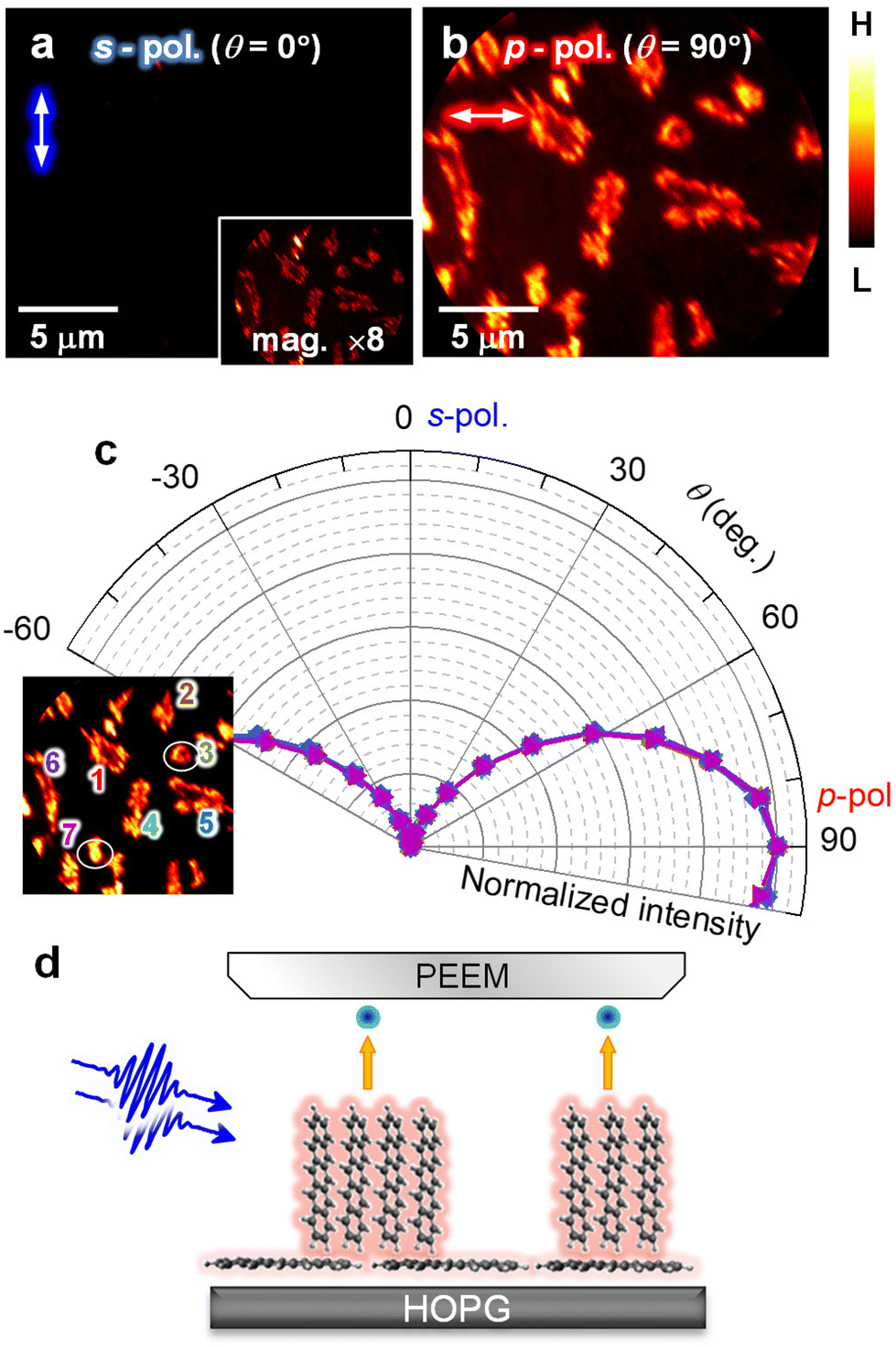 | ||
| Fig. 4 (a and b) 2P-PEEM (hv = 4.33 eV) of pentacene nanocrystals on HOPG (28 min deposition) taken with (a) s- and (b) p-polarized photons after heating treatment with 50 °C for 10 min. The 2P-PEEM intensity with s-polarized photons (a) is much weaker than that obtained with p-polarized photons (b) (see inset for magnified contrast). (c) 2P-PEEM intensity traces against θ analyzed at numbered nanocrystals (inset), where all nanocrystals get the highest 2P-PEEM intensity at p-polarized photons. (d) Schematic drawing of the crystal orientation of the pentacene nanocrystals after heating. | ||
As mentioned above, the pentacene molecules are selectively excited by a polarized photon that aligns with the long molecular axis at hv = 4.33 eV. Because p-polarized photons have the largest electromagnetic field perpendicular to the surface, the complete p-polarization selectivity indicates that nanocrystal rearrangements occur through mild thermal stimulation, forming another stable molecular orientation; the long molecular axis aligns perpendicular to the surface as a “standing-up” crystallization. A schematic illustration of the crystal orientation of pentacene after heating is shown in Fig. 4d.
Discussion
The polarization-dependent 2P-PEEM sensitively characterizes the orientation of pentacene nanocrystals on the HOPG substrate. Initially, the nanocrystals exhibit a molecular orientation of “lying flat”, which could donate excited electrons through the molecular π-orbital(s). They also undergo a complete transformation into a “standing up” orientation with a mild thermal treatment. The initial growth of the pentacene nanocrystals on graphite substrates has been widely studied with various experimental methods. For the pentacene nanocrystals on HOPG, scanning probe microscopy (SPM) shows that pentacene molecules align perpendicular to the surface with their long axis, a phenomenon known as the “thin film phase,”22,47 whose crystal alignments are typically observed on insulating or chemically inert substrates (e.g., SiO2,12 Al2O3,70 and polymers11,74). However, another SPM or spectroscopic study (e.g., X-ray diffraction,48 penning-ionization electron spectroscopy49) suggests that the pentacene molecular crystal is grown with the long axis of the molecules lying flat on the surface, similar to what is observed in metal substrates75 or reactive bare Si substrate.2Since the HOPG substrate is both conductive and chemically inert compared to metal or bare Si surfaces, it is inferred that the initial growth process is highly sensitive to various substrate conditions, such as cleanliness, temperature, deposition rate, surface flatness, and other factors, which have been extensively discussed in previous literature.47–50 Notably, Götzen et al.50 reported that both “lying-flat” and “standing-up” nanocrystals are formed separately on flat HOPG and Ar+-sputtered rough HOPG substrates, respectively. Our study has demonstrated that the transition of the molecular orientation from “lying flat” to “standing-up” occurs thermally, with the lying-flat molecular orientation initially grown on the clean HOPG substrate at ambient temperature, revealing the early stages of pentacene crystal formation on the HOPG substrate.
Conclusions
To conclude, we sensitively characterized the molecular orientation and ultrafast dynamics of electron transfer at a heterointerface between the electron-donating pentacene nanocrystal and HOPG substrate using 2P-PEEM. By selecting the resonant polarized photons, it is revealed that the pentacene nanocrystals initially grow with a lying-flat configuration, whose π-orbitals are connected to the substrate, facilitating a favorable transportation of photoexcited electrons. The time-resolved 2P-PEEM clearly images the excited electron dynamics at the substrate donated by pentacene nanocrystals within a timescale of ≈10 ps. The heating treatment induces the change in the molecular orientation into a standing-up orientation, suggesting that the controlled deposition of the organic molecule is crucial to fabricating fully-designed organic devices. Such real-space and temporal imaging of local photoexcited states will accelerate the technological advancement in organic electronics.Experimental
Sample preparation
To prepare an atomically flat and clean substrate, a HOPG substrate was cleaved in air and was heated to 700 K for 50 h in an ultrahigh vacuum (UHV) chamber (1 × 10⁻⁸ Pa). The cleanness was checked by taking a 2P-PES spectrum, showing a clear peak derived from an IPS (see Fig. 1c).76,77 Pentacene molecule (Sigma-Aldrich, ≥99.9%, sublimed grade) was deposited onto the cleaned HOPG substrate from a quartz effusion cell installed in the UHV system. The deposition rate was monitored using a quartz microbalance (INFICON, STM-5). The sample was then transferred to the 2P-PEEM system without breaking the UHV condition.2P-PEEM measurement
The lateral distribution of 2P-photoemission was imaged by a PEEM system (IS-PEEM, FOCUS GmbH) as 2P-PEEM. The third harmonics of a titanium sapphire laser (COHERENT, Mira 900-F, 76 MHz, 100 fs, hν = 1.35–1.63 eV) were used in the 2P-PEEM measurements, which were generated with a couple of beta barium borate crystals. The pulse duration and energy of the incident ultraviolet photons were 150 fs and 0.26 nJ per pulse (equivalent to an average power of 20 mW), respectively. The hν was typically set to 4.33 eV to effectively photoexcite the pentacene molecule (Fig. 2e). Light polarization of the incident laser was controlled by rotating at the azimuth angle of a half-wave plate. The laser beam was focused onto the surface through an MgF2 window at an incident angle of 75° (Fig. 2c) with respect to the surface normal.In the time-resolved 2P-PEEM, the laser beam was divided into two separate beams, and they were combined at the sample surface in a “skew” configuration (Fig. S7 in the ESI†). The delay time between both pulses was changed by an optical stage with 100 nm (0.33 fs) accuracy. The temporal resolution was estimated to be better than one-third of the pulse duration (<50 fs). No space charge effect causing degradation of the PEEM image was observed in this pulsed laser excitation study due to the use of a high-repetition (76 MHz) laser. To accurately evaluate the electronic states of the pentacene film, 2P-PES measurements were performed before and after 2P-PEEM experiments with a shared light source, in which the photoemitted electrons with a 2P-proccess were collected by a hemispherical electron energy analyzer (VG Scienta-3000). The sample temperature during the entire measurement was kept at 293 K.
Author contributions
Both M. S. and A. N. contributed to the experimental and writing processes. A. N. supervised the overall project.Conflicts of interest
There are no conflicts to declare.Acknowledgements
This work is partly supported by the program of Exploratory Research for Advanced Technology (ERATO) in Japan Science and Technology Agency (JST) entitled with “Nakajima Designer Nanocluster Assembly Project”, by JSPS KAKENHI of Grant-in-Aid for Scientific Research (A) No. 15H02002 and 19H00890, Scientific Research (B) No. 23H01939, and for Scientific Research (C) No. 18K04942, of Challenging Research No. 17H06226 and 21K18939, and of Transformative Research Areas (A) “Hyper–Ordered Structures Science” No. 21H05573. A. N. is grateful for the support from the Alexander von Humboldt Foundation.References
- J. Y. Tsao, Materials fundamentals of molecular beam epitaxy, Academic Press, San Diego, 1993 Search PubMed.
- F. J. Meyer zu Heringdorf, M. C. Reuter and R. M. Tromp, Nature, 2001, 412, 517–520 CrossRef CAS PubMed.
- D. Cahen, A. Kahn and E. Umbach, Mater. Today, 2005, 8, 32–41 CrossRef CAS.
- N. Koch, Chem. Phys. Chem., 2007, 8, 1438–1455 CrossRef CAS PubMed.
- S. Duhm, G. Heimel, I. Salzmann, H. Glowatzki, R. L. Johnson, A. Vollmer, J. P. Rabe and N. Koch, Nat. Mater., 2008, 7, 326–332 CrossRef CAS PubMed.
- P. M. Beaujuge and J. M. J. Fréchet, J. Am. Chem. Soc., 2011, 133, 20009–20029 CrossRef CAS PubMed.
- The molecule-metal interface, ed. N. Koch, N. Ueno and A. T. S. Wee, Wiley-VCH, Weinheim, Germany, 2013 Search PubMed.
- S. R. Forrest, Chem. Rev., 1997, 97, 1793–1896 CrossRef CAS PubMed.
- G. Witte and C. Wöll, Phys. Status Solidi A, 2008, 205, 497–510 CrossRef CAS.
- F. Schreiber, Phys. Status Solidi A, 2004, 201, 1037–1054 CrossRef CAS.
- W. H. Lee, J. Park, S. H. Sim, S. Lim, K. S. Kim, B. H. Hong and K. Cho, J. Am. Chem. Soc., 2011, 133, 4447–4454 CrossRef CAS PubMed.
- R. Ruiz, D. Choudhary, B. Nickel, T. Toccoli, K.-C. Chang, A. C. Mayer, P. Clancy, J. M. Blakely, R. L. Headrick, S. Iannotta and G. G. Malliaras, Chem. Mater., 2014, 16, 4497–4508 CrossRef.
- H. Ishii, K. Sugiyama, E. Ito and K. Seki, Adv. Mater., 1999, 11, 605–625 CrossRef CAS.
- S. Kera, H. Yamane and N. Ueno, Prog. Surf. Sci., 2009, 84, 135–154 CrossRef CAS.
- X.-Y. Zhu, Surf. Sci. Rep., 2004, 56, 1–83 CrossRef CAS.
- C. D. Lindstrom and X.-Y. Zhu, Chem. Rev., 2006, 106, 4281–4300 CrossRef CAS PubMed.
- T. Munakata, T. Sugiyama, T. Masuda, M. Aida and N. Ueno, Appl. Phys. Lett., 2004, 85, 3584–3586 CrossRef CAS.
- B. A. Collins and H. Ade, J. Electron Spectrosc. Relat. Phenom., 2012, 185, 119–128 CrossRef CAS.
- H. E. Martz, C. M. Logan, D. J. Schneberk and P. J. Shull, X-ray imaging: Fundamentals, industrial techniques and applications. Taylor and Francis, New York, 2016 Search PubMed.
- M. Feng, J. Zhao and H. Petek, Science, 2008, 320, 359–362 CrossRef CAS PubMed.
- R. Temirov, S. Soubatch, A. V. Luican and F. S. Tautz, Nature, 2006, 444, 350–352 CrossRef CAS PubMed.
- P. Parisse, M. Passacantando and L. Ottaviano, Appl. Surf. Sci., 2006, 252, 7469–7472 CrossRef CAS.
- M. Hollerer, D. Lüftner, P. Hurdax, Th. Ules, S. Soubatch, F. S. Tautz, G. Koller, P. Puschnig, M. Sterrer and M. G. Ramsey, ACS Nano, 2017, 11, 6252–6260 CrossRef CAS PubMed.
- T. Yamada and T. Munakata, Prog. Surf. Sci., 2018, 93, 108–130 CrossRef CAS.
- G. Ertl, Science, 1991, 254, 1750–1755 CrossRef CAS PubMed.
- M. Kim, M. Bertram, M. Pollmann, A. von Oertzen, A. S. Mikhailov, H. H. Rotermund and G. Ertl, Science, 2001, 292, 1357–1360 CrossRef CAS PubMed.
- S. Günther, B. Kaulich, L. Gregoratti and M. Kiskinova, Prog. Surf. Sci., 2002, 70, 187–260 CrossRef.
- N. M. Buckanie and F.-J. Meyer zu Heringdorf, Surf. Sci., 2007, 601, 1701–1704 CrossRef CAS.
- H. Marchetto, Th. Schmidt, U. Groh, F. C. Maier, P. L. Lévesque, R. H. Fink, H.-J. Freunda and E. Umbach, Phys. Chem. Chem. Phys., 2015, 17, 29150 RSC.
- C.-I. Lu, C.-H. Huang, K.-H. O. Yang, K. B. Simbulan, K.-S. Li, F. Li, J. Qi, M. Jugovac, I. Cojocariu, V. Feyer, C. Tusche, M.-T. Lin, T.-H. Chuang, Y.-W. Lan and D.-H. Wei, Nanoscale Horiz., 2020, 8, 1058–1064 RSC.
- J. Ziroff, F. Forster, A. Schöll, P. Puschnig and F. Reinert, Phys. Rev. Lett., 2010, 104, 233004 CrossRef CAS PubMed.
- F. Otto, T. Huempfner, M. Schaal, C. Udhardt, L. Vorbrink, B. Schroeter, R. Forker and T. Fritz, J. Phys. Chem. C, 2018, 122, 8348–8355 CrossRef CAS.
- N. M. Buckanie and F.-J. Meyer zu Heringdorf, Org. Electron., 2009, 10, 446–452 CrossRef CAS.
- K. Yamagiwa, M. Shibuta and A. Nakajima, Phys. Chem. Chem. Phys., 2017, 19, 13455–13461 RSC.
- M. Aeschlimann, T. Brixner, A. Fischer, C. Kramer, P. Melchior, W. Pfeiffer, C. Schneider, C. Strüber, P. Tuchscherer and D. V. Voronine, Science, 2011, 333, 1723–1726 CrossRef CAS PubMed.
- A. Hu, W. Liu, X. Li, S. Xu, Y. Li, Z. Xue, J. Tang, L. Ye, H. Yang, M. Li, Y. Ye, Q. Sun, Q. Gong and G. Lu, Nanoscale, 2021, 13, 2626–2631 RSC.
- M. Shibuta, K. Yamagiwa and A. Nakajima, Appl. Phys. Lett., 2016, 109, 203111 CrossRef.
- M. K. L. Man, A. Margiolakis, S. Deckoff-Jones, T. Harada, E. L. Wong, M. B. M. Krishna, J. Madéo, A. Winchester, S. Lei, R. Vajtai, P. M. Ajayan and K. M. Dani, Nat. Nanotechnol., 2017, 12, 36–40 CrossRef CAS PubMed.
- K. Yamagiwa, M. Shibuta and A. Nakajima, ACS Nano, 2020, 14, 2044–2052 CrossRef CAS PubMed.
- M. D
![[a with combining cedilla]](https://www.rsc.org/images/entities/char_0061_0327.gif) browski, Y. Dai and H. Petek, Chem. Rev., 2020, 120, 6247–6287 CrossRef PubMed.
browski, Y. Dai and H. Petek, Chem. Rev., 2020, 120, 6247–6287 CrossRef PubMed. - M. Hartelt, P. N. Terekhin, T. Eul, A.-K. Mahro, B. Frisch, E. Prinz, B. Rethfeld, B. Stadtmüller and M. Aeschlimann, ACS Nano, 2021, 15, 19559–19569 CrossRef CAS PubMed.
- R. Wallauer, M. Raths, K. Stallberg, L. Münster, D. Brandstetter, X. Yang, J. Güdde, P. Puschnig, S. Soubatch, C. Kumpf, F. C. Bocquet, F. S. Tautz and U. Höfer, Science, 2021, 371, 1056–1059 CrossRef CAS PubMed.
- G. Spektor, E. Prinz, M. Hartelt, A.-K. Mahro, M. Aeschlimann and M. Orenstein, Sci. Adv., 2021, 7, eabg5571 CrossRef PubMed.
- M. Shibuta and A. Nakajima, J. Phys. Chem. Lett., 2023, 14, 3285–3295 CrossRef CAS PubMed.
- E. Prinz, M. Hartelt, G. Spektor, M. Orenstein and M. Aeschlimann, ACS Photonics, 2023, 10, 340–367 CrossRef CAS.
- G. Spektor, D. Kilbane, A. K. Mahro, B. Frank, S. Ristok, L. Gal, P. Kahl, D. Podbiel, S. Mathias, H. Giessen, F.-J. Meyer zu Heringdorf, M. Orenstein and M. Aeschlimann, Science, 2017, 355, 1187–1191 CrossRef CAS PubMed.
- W. Chen, H. Huang, A. Thye and S. Wee, Chem. Commun., 2008, 4276–4278 RSC.
- N. Koch, A. Vollmer, I. Salzmann, B. Nickel, H. Weiss and J. P. Rabe, Phys. Rev. Lett., 2006, 96, 156803 CrossRef CAS PubMed.
- Y. Harada, H. Ozaki and K. Ohno, Phys. Rev. Lett., 1984, 52, 267402 CrossRef.
- J. Götzen, D. Käfer, C. Wöll and G. Witte, Phys. Rev. B: Condens. Matter Mater. Phys., 2010, 81, 085440 CrossRef.
- H. Petek and S. Ogawa, Prog. Surf. Sci., 1997, 56, 239–310 CrossRef CAS.
- J. Güdde and U. Höfer, Prog. Surf. Sci., 2005, 80, 49–91 CrossRef.
- J. Güdde, M. Rohleder, T. Meier, S. W. Koch and U. Höfer, Science, 2007, 318, 1287–1291 CrossRef PubMed.
- W.-L. Chan, M. Ligges, A. Jailaubekov, L. Kaake, L. Miaja-Avila and X.-Y. Zhu, Science, 2007, 334, 1541–1545 CrossRef PubMed.
- M. Bauer, A. Marienfeld and M. Aeschlimann, Prog. Surf. Sci., 2015, 90, 319–376 CrossRef CAS.
- X. Shi, W. You, Y. Zhang, Z. Tao, P. M. Oppeneer, X. Wu, R. Thomale, K. Rossnagel, M. Bauer, H. Kapteyn and M. Murnane, Sci. Adv., 2019, 5, eaav4449 CrossRef CAS PubMed.
- S. Ito, M. Schüler, M. Meierhofer, S. Schlauderer, J. Freudenstein, J. Reimann, D. Afanasiev, K. A. Kokh, O. E. Tereshchenko, J. Güdde, M. A. Sentef, U. Höfer and R. Huber, Nature, 2023, 616, 696–701 CrossRef CAS PubMed.
- W.-H. Soe, C. Manzano, A. De Sarkar, N. Chandrasekhar and C. Joachim, Phys. Rev. Lett., 2009, 102, 176102 CrossRef PubMed.
- H. Yamane, S. Nagamatsu, H. Fukagawa, S. Kera, R. Friedlein, K. K. Okudaira and N. Ueno, Phys. Rev. B: Condens. Matter Mater. Phys., 2005, 72, 153412 CrossRef.
- H. Fukagawa, H. Yamane, T. Kataoka, S. Kera, M. Nakamura, K. Kudo and N. Ueno, Phys. Rev. B: Condens. Matter Mater. Phys., 2006, 73, 245310 CrossRef.
- M. Shibuta, N. Hirata, R. Matsui, T. Eguchi and A. Nakajima, J. Phys. Chem. Lett., 2012, 3, 981–985 CrossRef CAS PubMed.
- M. Shibuta, N. Hirata, T. Eguchi and A. Nakajima, ACS Nano, 2017, 11, 4307–4314 CrossRef CAS PubMed.
- M. Muntwiler, Q. Yang, W. A. Tisdale and X.-Y. Zhu, Phys. Rev. Lett., 2008, 101, 196403 CrossRef PubMed.
- X.-Y. Zhu, Q. Yang and M. Muntwiler, Acc. Chem. Res., 2008, 42, 1779–1787 CrossRef PubMed.
- S. Berkebile, P. Puschnig, G. Koller, M. Oehzelt, F. P. Netzer, C. Ambrosch-Draxl and M. G. Ramsey, Phys. Rev. B: Condens. Matter Mater. Phys., 2008, 77, 115312 CrossRef.
- Y. Nakayama, S. Kera and N. Ueno, J. Mater. Chem. C, 2020, 8, 9090–9132 RSC.
- P. Sony and A. Shukla, Phys. Rev. B: Condens. Matter Mater. Phys., 2007, 75, 155208 CrossRef.
- T. M. Halasinski, D. M. Hudgins, F. Salama, L. J. Allamandola and Th. Bally, J. Phys. Chem. A, 2000, 104, 7484–7491 CrossRef CAS.
- R. Mondal, C. Tönshoff, D. Khon, D. C. Neckers and H. F. Bettinger, J. Am. Chem. Soc., 2009, 131, 14281–14289 CrossRef CAS PubMed.
- R. Forker, M. Gruenewald, T. Kirchhuebel and T. Fritz, Adv. Opt. Mater., 2021, 9, 2100200 CrossRef CAS.
- G. Moos, C. Gahl, R. Fasel, M. Wolf and T. Hertel, Phys. Rev. Lett., 2001, 87, 267402 CrossRef CAS PubMed.
- Y. Ishida, T. Togashi, K. Yamamoto, M. Tanaka, T. Taniuchi, T. Kiss, M. Nakajima, T. Suemoto and S. Shin, Non-thermal hot electrons ultrafastly generating hot optical phonons in graphite, Sci. Rep., 2011, 1, 64 CrossRef CAS PubMed.
- S. Kim, I. Jo, D. C. Dillen, D. A. Ferrer, B. Fallahazad, Z. Yao, S. K. Banerjee and E. Tutuc, Phys. Rev. Lett., 2012, 108, 116404 CrossRef PubMed.
- N. Koch, A. Elschner, J. P. Rabe and R. L. Johnson, Adv. Mater., 2005, 3, 17 Search PubMed.
- C. B. France, P. G. Schroeder, J. C. Forsythe and B. A. Parkinson, Langmuir, 2003, 19, 1274–1281 CrossRef CAS.
- M. Shibuta, K. Yamamoto, T. Ohta, M. Nakaya, T. Eguchi and A. Nakajima, Sci. Rep., 2017, 6, 35853 CrossRef PubMed.
- S. Tan, A. Argondizzo, C. Wang, X. Cui and H. Petek, Phys. Rev. X, 2017, 7, 011004 Search PubMed.
Footnotes |
| † Electronic supplementary information (ESI) available: Note S1, Fig. S1–S9, and Movies S1–S3. See DOI: https://doi.org/10.1039/d4nr00720d |
| ‡ Present address: Department of Physics and Electronics, Graduate School of engineering, Osaka Metropolitan University, 3-3-138 Sugimoto, Sumiyoshi-ku, Osaka 558-8585, Japan. |
| This journal is © The Royal Society of Chemistry 2024 |