
 Open Access Article
 This Open Access Article is licensed under a
 Creative Commons Attribution 3.0 Unported Licence
Photodetectors integrating waveguides and semiconductor materials
Xin-Xue
Wang
a,
Guang
Zeng
a,
Qiu-Jun
Yu
a,
Lei
Shen
a,
Cai-Yu
Shi
a and
Hong-Liang
Lu
 *ab
*ab
aState Key Laboratory of ASIC and System, Shanghai Institute of Intelligent Electronics & Systems, School of Microelectronics, Fudan University, Shanghai 200433, China. E-mail: honglianglu@fudan.edu.cn
bJiashan Fudan Institute, Jiaxing, Zhejiang Province 314100, China
First published on 9th February 2024
Abstract
Photodetectors integrating substrates and semiconductor materials are increasingly attractive for applications in optical communication, optical sensing, optical computing, and military owing to the unique optoelectronic properties of semiconductor materials. However, it is still a challenge to realize high-performance photodetectors by only integrating substrates and semiconductor materials because of the limitation of incident light in contact with sensitive materials. In recent years, waveguides such as silicon (Si) and silicon nitride (Si3N4) have attracted extensive attention owing to their unique optical properties. Waveguides can be easily hetero-integrated with semiconductor materials, thus providing a promising approach for realizing high-performance photodetectors. Herein, we review recent advances in photodetectors integrating waveguides in two parts. The first involves the waveguide types and semiconductor materials commonly used to fabricate photodetectors, including Si, Si3N4, gallium nitride, organic waveguides, graphene, and MoTe2. The second involves the photodetectors of different wavelengths that integrate waveguides, ranging from ultraviolet to infrared. These hybrid photodetectors integrating waveguides and semiconductor materials provide an alternative way to realize multifunctional and high-performance photonic integrated chips and circuits.
1. Introduction
Silicon (Si) photodetectors have become very popular in many integrated photonics applications because of their mature CMOS compatibility, outstanding photoelectric characteristics, and unique advantages of high integration density.1–3 However, because of the inherent material properties of Si, it is very challenging to prepare active photodetectors. Thus, to improve the drawbacks of Si, introducing some other semiconductor materials and integrating them with Si has attracted considerable attention as a promising solution.4,5 Based on this strategy, in the past decade, researchers have attempted to design and fabricate photodetectors integrating Si with different semiconductor materials, including III–V semiconductor materials,6,7 germanium,8 and two-dimensional (2D) semiconductor materials.9,10 In addition, controlled by self-limiting surface reactions, the atomic layer deposition (ALD) method, a unique preparation process, can be employed to grow 2D semiconductors with high precision, wafer level, and good uniformity and thus widely used in the fields of integrated circuits and optoelectronics.11 For example, ALD-fabricated photodetectors based on monolayer tungsten trioxide (WO3) have exhibited outstanding optoelectronic properties.12,13 However, as the incident light enters a photodetector from the outside of the photodetector, it is difficult to achieve on-chip integration for photodetectors that only integrate Si and semiconductor materials. Thus, to achieve integrated photoelectric chips, photodetectors integrating waveguides and semiconductor materials have attracted increasing attention as a promising solution.14–16Fig. 1 shows an outline of this article, which mainly reviews the advanced work on photodetectors integrating waveguides and semiconductor materials, focusing on waveguide materials, waveguide types, semiconductor materials and integrated-waveguide photodetector types. Firstly, various waveguides and semiconductor materials are employed in the fabrication of integrated waveguide photodetectors, including Si, silicon nitride (Si3N4), gallium nitride (GaN), organic waveguides, graphene,17–22 MoTe2, black phosphorus (BP), carbon nanotubes, and palladium selenide (PdSe2).23–29 Secondly, the waveguide type is further divided into end-coupled waveguide, grating coupled waveguide, and ring waveguide.30–32 Thirdly, the reported photodetectors with integrated waveguides mainly include infrared (IR) photodetectors, visible (VIS) photodetectors, and ultraviolet (UV) photodetectors.33–38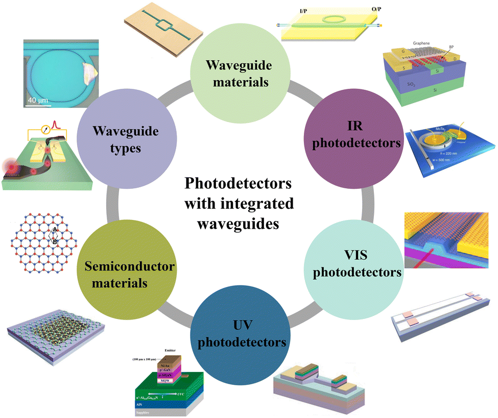 | ||
| Fig. 1 Schematic summary of waveguide materials (reproduced with permission from ref. 21 and 22. Copyright 2022 and 2015, Wiley-VCH and the American Chemical Society, respectively), semiconductor materials (reproduced with permission from ref. 27 and 28. Copyright 2016 and 2020, Wiley-VCH, respectively), waveguide types (reproduced with permission from ref. 31 and 32. Copyright 2020 and 2023, De Gruyter and the American Chemical Society, respectively), and photodetector types of integrated waveguides (reproduced with permission from ref. 34–38. Copyright 2015, 2020, 2023, 2018, and 2022, Springer Nature, Wiley-VCH, IEEE, and Elsevier, respectively). | ||
Photodetectors integrating waveguides and semiconductor materials effectively extend the length of the interaction of light-sensitive materials. Thus, they are expected to achieve many important and extensive applications in the fields of optical communication,39 imaging,40 and sensing.41 In recent years, it has been demonstrated that high-performance photodetectors integrating waveguides can achieve detection in the ultraviolet (UV) to infrared (IR) region.42–44 At present, the waveguide materials employed in the fabrication of photodetectors are mainly Si, Si3N4, GaN, lithium cyanate (LN), and ZnO,45–49 which transmit IR, VIS, and UV light, respectively, due to their inherent properties. Since the first successful exfoliation of graphene in 2004,50 two-dimensional (2D) semiconductor materials have attracted increasing attention in photoelectric detection due to their unique structure and physical properties. Currently, some 2D materials have been used in the field of waveguide photodetectors, including graphene,51 BP,52 MoTe2,53 and carbon nanotubes.54 Further, 2D materials can be conveniently transferred to the waveguide substrate via the wet transfer or dry transfer process.55,56 In this case, lattice matching can be easily achieved. However, due to the small band gap of 2D materials, there is no report on hybrid waveguide/2D material UV photodetectors. In contrast, there have been reports on high-performance UV photodetectors integrating waveguides and 3D semiconductor materials.57 Consequently, photodetectors integrating waveguides and semiconductor materials are increasingly attractive for many applications.
Herein, we review photodetectors with integrating waveguide and semiconductor materials. In the second section, the main waveguide materials, waveguide structure, and semiconductor materials for waveguide photodetectors are introduced. In the third section, we review the recent progress on photodetectors with integrated waveguide and semiconductor materials for wavelength bands ranging from UV to IR. Finally, we present conclusions and prospects on the future work of integrated waveguide and semiconductor material photodetectors.
2. Waveguide types and semiconductor materials used for photodetectors
2.1 Waveguide materials and types commonly used for photodetectors
With the development of highly integrated chips, photodetectors based on waveguides have been further investigated to achieve more compact circuits. Photodetectors integrating waveguides can combine high operational speed and high quantum efficiency simultaneously. This is due to the longer optical absorption length of waveguide-integrated detectors. At this stage, silicon-based waveguides are significantly studied and used to achieve low-loss, low power consumption, small size of the devices and high integrated circuits. Another commonly used waveguide material, Si3N4, is also widely used in the field of photoelectric detection. Researchers have conducted some studies on the different structural types of the above-mentioned two commonly used waveguide materials.Schall et al.58 fabricated photodetectors with an integrated Si waveguide and graphene, which were capable of operating in the 1550 nm band. As shown in Fig. 2a, a 400 nm-wide ridged Si waveguide was produced on 220 nm-thick silicon and covered with a 3 μm buried oxide layer. The fiber loss in the silicon waveguide was only 13.5 dB. The ridge waveguide is a common Si waveguide structure. Another structure of Si waveguides, i.e., buried waveguide, has also been studied by researchers. Shiue et al.59 prepared hBN/single layer graphene (SLG)/hBN photodetectors with an integrated buried Si waveguide. As shown in Fig. 2b, the 520 nm-wide Si waveguide was buried among SOI wafers by a shallow channel isolation process. The buried waveguide enabled a flatter interface between the planar waveguide and the 2D material because the SiO2 layer filling could be used in this structure.
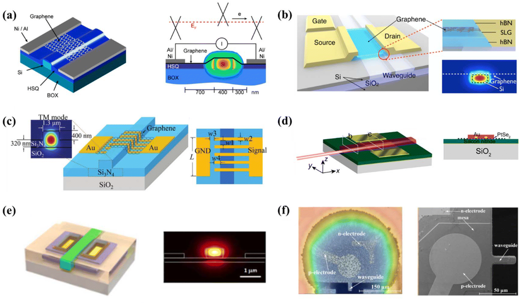 | ||
| Fig. 2 Waveguide materials and types commonly used in integrated waveguide photodetectors. (a) Photodetector with integrated ridge Si waveguide. Reproduced with permission from ref. 58. Copyright 2014, the American Chemical Society. (b) Photodetector with integrated buried Si waveguide. Reproduced with permission from ref. 59. Copyright 2015, the American Chemical Society. (c) Photodetector with integrated ridge Si3N4 waveguide. Reproduced with permission from ref. 30. Copyright 2018, the Royal Society of Chemistry. (d) Photodetector with integrated buried Si3N4 waveguide. Reproduced with permission from ref. 64. Copyright 2020, the American Chemical Society. (e) Photodetector with integrated chalcogenide glass waveguide. Reproduced with permission from ref. 66. Copyright 2018, Optical Society of America. (f) Photodetector with integrated InGaN/GaN waveguide. Reproduced with permission from ref. 67. Copyright 2016, Optical Society of America. | ||
Another common material for waveguides, Si3N4, has been used in studies with the two above-mentioned structures. A ridge-based Si3N4 waveguide photodetector integrated with graphene was prepared by Gao et al.,30 which could detect 1550 nm IR light. The Si3N4 waveguide was obtained by chemical vapor deposition (CVD). As shown in Fig. 2c, the raised spine portion of the Si3N4 waveguide is 450 μm long, 1.3 μm wide, and 400 nm high. The SLG directly covers the Si3N4 waveguide and the metal electrode, and the built-in electric field between the metal–graphene junction is beneficial for the separation and transport of photogenerated carriers, and the multiple metal contacts shorten the transmission distance and time of photogenerated carriers. Wang et al.64 integrated a buried Si3N4 waveguide with PtSe2 photodetector, as shown in Fig. 2d. The use of a ridge waveguide has the tendency to break the 2D material and the deformation at the ridge edges reduces its carrier mobility. Alternatively, buried waveguides can effectively avoid this problem, and thus avoid degrading the properties of the material.
In addition to the common Si and Si3N4 waveguides, Li et al.66 investigated a flexible photodetector based on a chalcogenide glass waveguide, as shown in Fig. 2e. The presence of the flexible waveguide enhances the interaction between matter and light. At 1530 nm, the device has a noise equivalent power of only 0.02 pW Hz1/2 and responsivity of 0.35 A W−1, achieving an external quantum efficiency of 28%. As shown in Fig. 2f, a suspended waveguide photodetector with InGaN/GaN multiple quantum wells was fabricated.67 The prepared photodetectors were highly responsive to VIS light at 401 and 435 nm at different voltages, respectively. These results provide a hopeful approach for the development of suspended waveguide photodetectors for various applications in the visible region. To strengthen the comparison between different types of waveguides, we organized a figure of merit table, as shown in Table 1, comparing some parameters such as band gap, refractive index, transmission band, and loss. Waveguide loss is defined as the optical power lost during the transmission of light waves within a waveguide, which has a significant impact on the application of waveguide materials.64,68 It imposes limitations on the transmission distance of light within the waveguide. Additionally, waveguide loss results in energy wastage, thereby diminishing the overall efficiency of waveguide-based optical communication and sensing systems. According to Table 1, the characteristics of each waveguide material can be clearly distinguished.
| Waveguide | Bandgap (eV) | Effective refractive index | Transmission band | Loss | Ref. |
|---|---|---|---|---|---|
| Si | ∼1.1 | ∼3.0 (channel waveguides), ∼2.0 (ridge waveguides) | IR (1.3–1.6 μm) | ∼3.6 dB cm−1 | 60–63 |
| Si3N4 | ∼5–6 | ∼2.0 | UV-IR | ∼4.5 dB cm−1 | 64, 65 |
| Chalcogenide glass | — | — | IR (1–3.0 μm) | — | 66 |
| InGaN/GaN multiple quantum wells | ∼2.5–3.5 | ∼2.5 | UV-blue light | — | 67 |
2.2 Semiconductor materials for photodetectors with integrated waveguides
Since the discovery of graphene in 2004, 2D materials have gradually entered the field of research, opening up new possibilities for the development of high-performance photodetectors. Compared to bulk materials, 2D materials with atomically thin limiting thicknesses are capable of enormous quantum effects, which endow them with unique structures and many excellent capabilities, especially in terms of electronic and optoelectronic properties.9 2D materials have high mechanical strength and good flexibility, can be adapted to a wide range of substrate materials, and are well suited for mature CMOS processing, enabling the large-scale integration of silicon photonic structures. Alternatively, 2D materials have high carrier mobility and no dangling bonds, which can very effectively suppress the dark current of photodetectors and realize room temperature detection with high sensitivity and high-speed photoelectric response.24Fig. 3 displays the relationship between 2D materials and the corresponding detection bands.69 According to Fig. 3, it is obvious that some 2D materials have an extremely small intrinsic band gap, such as BP and graphene. In addition, photodetectors integrating these materials are capable of reaching an extremely wide detection spectral range, up to the mid-infrared and even terahertz bands. Thus, the use of 2D materials to achieve a broad-spectrum photoelectric response is very beneficial for the application of these types of photodetectors.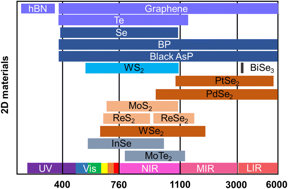 | ||
| Fig. 3 Relationship between 2D materials and the corresponding detection bands. Reproduced with permission from ref. 69. Copyright 2021, Wiley-VCH. | ||
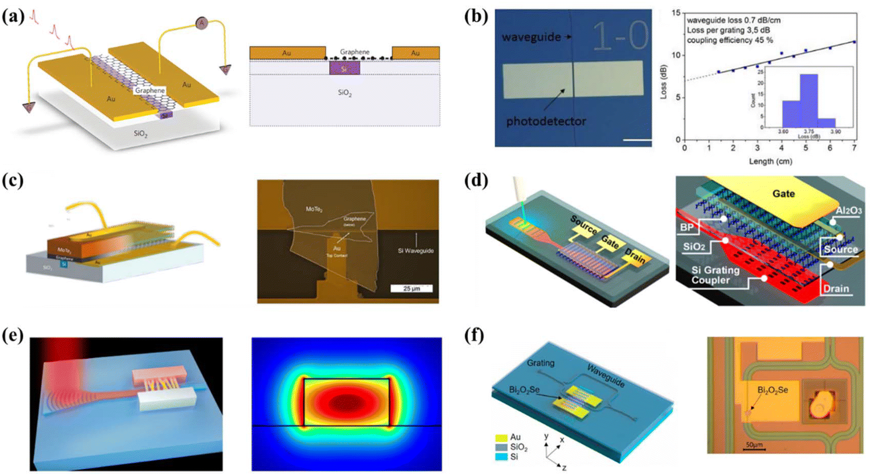 | ||
| Fig. 4 Semiconductor materials commonly used for integrated waveguide photodetectors. (a) Integrated waveguide photodetector with SLG. Reproduced with permission from ref. 71. Copyright 2013, Springer Nature. (b) Integrated waveguide photodetector with multilayer graphene. Reproduced with permission from ref. 72. Copyright 2018, Optical Society of America. (c) Integrated waveguide photodetector with the graphene/MoTe2 heterojunction. Reproduced with permission from ref. 74. Copyright 2019, Optical Society of America. (d) Integrated waveguide photodetector with BP. Reproduced with permission from ref. 73. Copyright 2018, the American Chemical Society. (e) Integrated waveguide photodetector with carbon nanotubes. Reproduced with permission from ref. 75. Copyright 2020, the American Chemical Society. (f) Integrated waveguide photodetector with Bi2O2Se. Reproduced with permission from ref. 76. Copyright 2021, the American Chemical Society. | ||
![[thin space (1/6-em)]](https://www.rsc.org/images/entities/char_2009.gif) 000 cm2 V−1 s−1) and intrinsic optical response time at room temperature, carbon nanotubes can be used in a wide range of high-speed electronic and optoelectronic devices, including photodetectors. As shown in Fig. 4f, Lin et al. designed and fabricated photodetectors integrating waveguides and Bi2O2Se.76 Bi2O2Se was first grown on mica by CVD, and then well integrated with the Si waveguide via the transfer method. Meanwhile, the narrow band gap of Bi2O2Se can be used in the study of high-performance near-IR photodetectors.
000 cm2 V−1 s−1) and intrinsic optical response time at room temperature, carbon nanotubes can be used in a wide range of high-speed electronic and optoelectronic devices, including photodetectors. As shown in Fig. 4f, Lin et al. designed and fabricated photodetectors integrating waveguides and Bi2O2Se.76 Bi2O2Se was first grown on mica by CVD, and then well integrated with the Si waveguide via the transfer method. Meanwhile, the narrow band gap of Bi2O2Se can be used in the study of high-performance near-IR photodetectors.
3. Waveguide-integrated photodetectors for different wavelengths
Since the emergence of 2D materials, 2D materials represented by graphene have been increasingly studied in various fields, including gas sensing,78 medicine,79 optoelectronics,80 and composite materials.81 Especially, 2D materials have received extensive attention in the field of photodetection in recent years due to their unique properties. A photodetector is a light sensor that can convert absorbed light signals into electrical signals and is widely used in optoelectronic systems,82 communications,83 aerospace,84 medical sterilization,85 fire prevention,86 the military,87 and other fields. At present, photodetectors corresponding to different wavelengths play an important role in optical systems in various fields. Therefore, the development of high-performance photodetectors has received increasing attention. Compared with traditional photodetectors based on 3D semiconductor materials, such as silicon,88 germanium,89 and III–V semiconductor materials,90 photodetectors based on 2D materials are ultra-thin and have high response, outstanding photo-dark current ratio, ultra-high electronic mobility and other advantages. These photodetectors can be classified into UV, visible, and IR photodetectors in terms of their detection wavelength. Further, UV photodetectors are divided into near UV (UVC), far UV (UVB), ultra-short UV (UVA), deep UV (DUV), and extreme UV (EUV) photodetectors according to the wavelength range. Similarly, IR photodetectors can be classified into near-IR (NIR), mid-IR (MIR), and far-IR (FIR) photodetectors according to the wavelength. Alternatively, from the perspective of typical detection principles,91 photodetectors for 2D materials can be classified into photo-bolometric (PB) effect, photothermoelectric (PTE) effect, photovoltaic (PV) effect, and photoconductive (PC) effect. In the case of the PTE effect, the photocurrent is generated by photon-induced temperature changes in a 2D material. The PB effect refers to the mechanism by which the temperature of the 2D material changes due to light illumination, thereby causing the resistance of the material to change.92 Regarding the PTE effect, it is a mechanism by which light-induced temperature gradients generate photocurrents.93 The PV effect is a mechanism by which a 2D material generates additional electron–hole pairs separated by a built-in electric field due to illumination.94 The PC effect refers to the mechanism by which the electrical conductivity of a 2D material increases due to the photogenerated carriers generated by illumination.95 The principles of photodetectors corresponding to different 2D materials and different device structures are often not single, but one or several combinations. In addition, from the perspective of the structure of photodetectors, photodetectors based on 2D materials can be divided into two categories. One is a photodetector with 2D materials combined with substrates such as Si, sapphire, and silicon carbide, and the other is a photodetector with 2D materials combined with substrates such as Si, Si3N4, and GaN waveguides. Currently, some researchers reviewed the first class of photodetectors.96 However, it is well known that for 2D materials, taking graphene as an example, it is difficult to achieve high photoresponsivity due to its low absorptivity to incident light (∼2.3%). Under this premise, the performance of the first type of photodetectors with the hetero-combination of 2D materials and substrates needs to be further improved due to the limited interaction length between 2D materials and light. As an alternative, the second type of photodetectors integrating 2D materials and waveguides will overcome the above-mentioned problem. In addition, because 2D materials are relatively thin, they can be employed in the evanescent field of waveguide transmission light, and thus the absorption of the incident light by the 2D material can be enhanced, and thus the performance of the photodetector can be improved. In the following part, we review photodetectors for different wavelengths. Furthermore, the parameters corresponding to the photodetectors integrating waveguides and semiconductors are summarized in Table 2.| Materials | Waveguide | Wavelength (μm) | Photodetector type | Bias (V) | Responsivity (A W−1) | Bandwidth (GHz) | Ref. |
|---|---|---|---|---|---|---|---|
| Graphene | Si | 1.55 | MSM | 1 | 0.108 | >20 | 71 |
| Graphene | Si | 1.55 | MSM | 0 | 6 × 10⁻³ | 41 | 58 |
| Graphene | Si | 1.31–1.65 | MSM | 0 | 0.03 | 18 | 105 |
| Graphene | Si | VIS-2.75 | Graphene–Si | −1.5 | 0.13 | — | 116 |
| Graphene | Si | 1.55 | MSM | 0.4 | 0.057 | 7.7 | 149 |
| Graphene | Si | 1.55 | MSM | 1.2 | 0.36 | 42 | 59 |
| Graphene | Si | 1.55 | MSM | 0 | 0.035 | 65 | 150 |
| Graphene | Si | 1.55 | MSM | 1 | 1 × 10⁻³ | 76 | 151 |
| Graphene | Si | 1.55 | MSM | 2 | 0.273 | — | 104 |
| Graphene | Si | 1.55 | MSM | 2.2 | 0.36 | 110 | 152 |
| Graphene | Si | 6.3–7.1 | MSM | 0 | 8 × 10⁻³ | — | 106 |
| Graphene | Si | 1.55 | FET | −0.3 | 0.4 | 40 | 108 |
| BP | Si | 1.55 | MSM | 0.4 | 0.135 | 3 | 153 |
| BP | Si | 2 | MSM | 0.4 | 0.307 | 1.33 | 154 |
| MoTe2 | Si | 1.1–1.2 | p–n junction | 0 | 1 × 10⁻³ | — | 107 |
| MoTe2 | Si | 1.3 | Graphene–MoTe2 | −0.6 | 0.14 | 25 | 60 |
| Graphene | Si3N4 | 1.55 | MSM | 0 | 0.015 | 30 | 113 |
| Graphene | Si3N4 | 1.55 | MSM | 1 | 2.36 | 33 | 114 |
| Graphene | Si3N4 | 1.55 | p–n junction | 0 | 12.2 (V W−1) | 42 | 117 |
| Graphene | Si3N4 | 1.55 | p–n junction | 0 | 6 (V W−1) | 67 | 118 |
| PtSe2 | Si3N4 | 1.55 | MSM | 8 | 12 | 35 | 120 |
| InAlAs/InGaAs | Glass | 1.53 | MSM | — | 0.25 | 1.4 | 131 |
| MoS2 | Si3N4 | 0.532 | FET | 30 | 0.44 | — | 123 |
| Si | Si3N4 | 0.85 | p–i–n | 20 | 0.1 | — | 124 |
| MoS2 | Si3N4 | 0.647 | FET | 1 | 1000 | — | 127 |
| MoSe2 | Si3N4 | 0.78 | MoSe2–WS2 | 2 | 1 | — | 128 |
| ZnO | ZnO | 0.3–0.7 | — | 1 | — | – | 148 |
| AlxGa1−xN | AlxGa1−xN | 0.28 | p–n junction | — | 0.3 | — | 33 |
3.1 Waveguide-integrated IR photodetectors
IR photodetectors are very important photodetectors, which have been widely used in various fields of human life, including the military,97 optical communication,98 night vision,99 imaging,100 thermal imaging cameras,101 medical treatment,102 and environmental monitoring.103 Therefore, 2D materials and waveguide-integrated IR photodetectors have attracted increasing attention in the past decade. In 2013, Kurz et al. designed and fabricated a metal–semiconductor–metal (MSM) IR photodetector integrating a waveguide and SLG,58 as shown in Fig. 2a. This IR photodetector is the first reported photodetector integrating waveguides and 2D materials according to our Web of Science search. The described photodetector with a good responsivity of 0.1 A W−1 and 3 dB bandwidth of >20 GHz can be a promising candidate in the field of optical communication (1550 nm). Then, in 2014, another MSM-structured photodetector integrating a waveguide and CVD-grown graphene was reported by Schall et al.,72 as shown in Fig. 4b. The IR photodetector (1550 nm) has a −3 dB bandwidth of 41 GHz and can detect data signals up to 50 Gbit per s. Two years later, Wang et al. reported the fabrication of an MSM photodetector (1550 nm) based on graphene and silicon slot waveguides,104 as shown in Fig. 5a. Compared with the previous MSM structure detector, the silicon slot waveguide structure can enhance the light intensity and reduce the mode confinement of the transmitted light, which increases the interaction between graphene and incident light. Simultaneously, efficient electron cooling and phonon scattering are lacking in suspended graphene. Consequently, the waveguide achieved an absorption of 0.935 dB μm−1 at 1550 nm and a maximum responsivity of 0.273 A W−1 in the communication band. Considering a single-communication-band photodetector, Pospischil et al. demonstrated an ultra-wideband complementary metal–oxide semiconductor (CMOS)-compatible IR photodetector based on graphene and Si waveguide,105 as depicted in Fig. 5b. This photodetector could detect almost all fiber optic telecommunication bands and carry a multi-gigahertz operation. Subsequently, Ma et al. designed an MSM photodetector integrating graphene and Si waveguides with a CaF2 substrate as the waveguide cladding,106 as shown in Fig. 5c. Compared with other waveguide cladding materials, although the photon energy of long-wave infrared (LWIR) is very low, the transmission loss of the Si waveguide based on the CaF2 cladding for LWIR is very low. Therefore, this photodetector showed low loss over a broad LWIR wavelength range of 6.3–7.1 μm. In addition, the photodetector also achieved a broadband responsivity of about 8 mA W−1 in the LWIR wavelength at zero bias.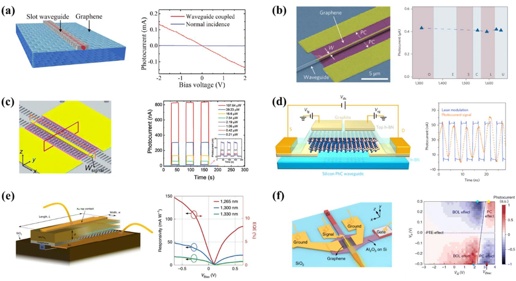 | ||
| Fig. 5 IR photodetector integrated with Si waveguide and 2D materials. (a) Graphene photodetector with integrated Si slot waveguide. The photocurrent measurement of normal incident and waveguide coupling at 0.5 mW as a function of the bias voltage is shown on the right. Reproduced with permission from ref. 104. Copyright 2016, the Royal Society of Chemistry. (b) Waveguide-integrated graphene photodetector. Photocurrent as a function of the optical communication band is shown on the right. Reproduced with permission from ref. 105. Copyright 2013, Springer Nature. (c) Waveguide-integrated graphene photodetector with CaF2 substrate. The right shows the temporal photoresponses under different incident powers. Reproduced with permission from ref. 106. Copyright 2021, the American Chemical Society. (d) Encapsulated bilayer MoTe2 photodetector is integrated on a silicon photonic-crystal waveguide with a p–n junction. On the right is the dynamic photocurrent under zero bias voltage. Reproduced with permission from ref. 107. Copyright 2017, Springer Nature. (e) Vertical MoTe2–graphene heterostructure photodetector with Si waveguide. The functional relationship between light response and EQE with applied bias at different wavelengths is shown on the right. Reproduced with permission from ref. 60. Copyright 2020, Springer Nature. (f) Si–graphene hybrid plasmonic waveguide photodetector in 1.55 and 2 μm. The measured photocurrent map as VG and Vb vary is shown on the right. Reproduced with permission from ref. 108. Copyright 2020, Springer Nature. | ||
Notably, it is well known that photodetectors with MSM structures integrated with 2D materials are relatively simple to fabricate. On the one hand, the dark current of these photodetectors is generally large and their response time is relatively long. On the other hand, due to the extended length of the absorption region of the 2D material and the waveguide to transmit light, the photodetector footprint and capacitance will increase, which also hinders the high-speed operation of carriers in the 2D material.96 The above-mentioned two drawbacks are challenges for realizing high-performance photodetectors. Thus, to overcome these drawbacks, photodetectors such as diodes, heterojunctions, and field effect transistors (FETs) can be considered. Because a diode device can make the dark current of the photodetector very small due to the existence of a depletion region potential barrier, the heterojunction device can shorten the response time of the photodetector due to the built-in electric field of the device. Owing to the regulation of the gate voltage, FET devices can achieve a small dark current, high responsivity, and shortened response time. In 2017, Bie et al. designed and fabricated light-emitting diodes and IR photodetectors (1100 nm) with an integrated Si waveguide and MoTe2,107 as shown in Fig. 5d. It is well known that for photonic devices, the performance of photodetectors is a challenge faced by researchers. Considering this challenge, the p–n junction photonic device integrating bilayer MoTe2 and Si waveguide can be used as a multifunctional photonic device. Consequently, the detection wavelength of this photodetector covers the range of 1100–1200 nm, and the maximum responsivity occurs at around 1160 nm with 5 mA W−1. Compared with this work, Flöry et al. designed and fabricated a photodetector at telecom wavelengths integrating an Si waveguide and MoTe2–graphene heterojunction,60 as shown in Fig. 5e. This photodetector achieved a record-high measurement bandwidth (at least 24 GHz) at a bias voltage of −3 V. In addition, Flöry et al. also studied the effect of different thicknesses of MoTe2 flakes on the performance of photodetectors and found that the photodetectors corresponding to thicker MoTe2 flakes have higher photoresponsivity. This is due to the fact that the thicker MoTe2 flakes have higher light absorption. Further, given that the photodetector is a vertical heterostructure device, the photodetector can confine the transmission path length of photogenerated carriers to a few nanometers, thereby achieving a shorter transmission time. Therefore, the photodetector achieved high-speed and high-performance targets with a record bandwidth and a high response of 0.2 A W−1 at 1300 nm.
Compared with diode devices and heterojunction devices, although the process of FET devices is more complicated, due to the good control of the gate to the channel, the photogenerated electron–hole pairs can be separated faster under the longitudinal electric field, and thus FET photodetectors have the advantages of small dark current and fast response simultaneously. In 2020, Guo et al. reported the fabrication of an FET photodetector based on an Si waveguide, graphene, and Al2O3,108 as shown in Fig. 5f. The plasmonic waveguide photodetector exhibited an excellent photoelectric performance in the wavelength range of 1.55 μm and beyond. It is worth noting that the photodetector has many novel designs. Firstly, the Si waveguide is ultra-thin and very wide, enhancing the absorption of transmitted light by graphene. Besides, placing a narrow metal strip on top of the Si waveguide, due to the local surface plasmon resonance effect and the very narrow metal strip, can reduce the absorption of the transmitted light by the metal and enhance the absorption of graphene, and thus the absorption coefficient of graphene can reach 0.23 dB μm−1. Further, the presence of gate control improves the performance of the plasmonic waveguide photodetector. Based on these optimized designs, the photodetector exhibited a setting-limited 3 dB bandwidth of >40 GHz and high responsivity of 0.4 A W−1 at 1.55 μm and bias voltage of −0.3 V. While operating at 2 μm, the device had a broad 3 dB bandwidth of >20 GHz (setup-limited) and a responsivity of 70 mA W−1 at −0.3 V bias. It should be noted that given that graphene is a 0-bandgap 2D material, graphene photodetectors operating in PC mode inevitably have higher dark currents. Alternatively, BP is a direct bandgap material with ∼0.3 eV in bulk and 1.8–2 eV in monolayer form,109,110 which can be used for broadband photodetection. In addition, compared with graphene, BP has a higher absorption rate.96 In 2019, Huang et al. presented an FET mid-IR photodetector (3.06–4.03 μm) integrating an Si waveguide and BP,73 as depicted in Fig. 4d. Under a bias of 1 V, this high-performance photodetector achieved an ultra-high responsivity of 23 A W−1 at 3.68 μm and 2 A W−1 at 4 μm. Furthermore, the noise equivalent power of this BP photodetector was less than 1 nW Hz−1/2 at 1 V and room temperature. The fabrication of these photodetectors integrated with Si waveguides and 2D materials provides a potential way to realize the design and fabrication of on-chip photonic integrated chips for applications in optical communication systems,39 sensing,41 imaging,40 and other fields.
It is worth noting that for electronic devices, Si has a leakage phenomenon because it is a semiconductor material, which will lead to the poor performance of the fabricated photodetectors integrating Si waveguides and 2D materials.111 Alternatively, given that the band gap of Si materials is relatively small, Si waveguides transmit incident light with wavelengths between 1000 and 1550 nm better.112 Regarding incident light in other wavelength bands, the loss of Si waveguides increases. Thus, to solve the above-mentioned two problems simultaneously, the Si3N4 waveguide is a better alternative. In 2018, Gao et al. designed and fabricated an MSM photodetector integrating Si3N4 waveguides and graphene deposited by CVD,113 as shown in Fig. 6a. Compared with the Si waveguide photodetector, the Si3N4 photodetector can block the leakage of carriers into the waveguide and reduce the transmission loss, thereby improving the photoresponse of the photodetector. Further, the IR photodetector innovatively adopts a metal–graphene junction design that increases the interaction between evanescent light and graphene, thereby doubling the responsivity of the photodetector. According to this design, the photodetector achieved a 30 GHz bandwidth and an intrinsic responsivity of 15 mA W−1 at ∼1550 nm and zero bias, which is comparable to that obtained with the best pristine graphene-based photodetectors. Next, Gao et al. improved the metal–graphene junction photodetector and fabricated a grating-like metal contact photodetector (1550 nm) integrating an Si3N4 waveguide and graphene,30 as depicted in Fig. 2c. The resistance–capacitance limited bandwidth of the fabricated device improved because of the relatively small relative permittivity of the Si3N4 material. Besides, the IR photodetector innovatively adopts a grating-shaped metal electrode design, which reduces the distance of carrier transmission between the two metal electrodes. Based on this design, a transit time-limited bandwidth of 111 GHz was calculated. Alternatively, for the actual device, it was experimentally found that at 1550 nm, the photodetector has an electro-optical bandwidth of 38 GHz under 0 V bias and an intrinsic responsibility of 13 mA W−1 under 0.1 V reverse bias. During the same period, to further improve the performance of the photodetector integrating a waveguide and graphene, Gao et al. demonstrated a novel photodetector integrating an Si3N4 waveguide and graphene with interdigitated electrode contacts,114 as shown in Fig. 6b. Based on this design, the photodetector exhibits two detection mechanisms (photovoltaic effect and photoconductivity effect) under different bias voltages. In the case of the photovoltaic effect, efficient photodetection is mainly achieved by separating photogenerated carriers through the action of a built-in electric field. Given that the region where the metal–graphene junction and band bending exist is small,115 it is usually much smaller than the distance between the two electrodes. Alternatively, the photogenerated carriers in graphene have a relatively short lifetime,116 and a large number of carriers is recombined before reaching the contact electrodes. The above-mentioned two problems limit the responsivity of graphene photodetectors. Thus, to overcome these problems, the interdigitated metal contacts employ an interdigital spacing as narrow as 200 nm. At zero bias, the built-in electric field can accelerate the carriers to saturation drift velocity. By increasing the bias voltage, the device can also perform photodetection under the photoconductor mechanism. Consequently, at zero bias and 1550 nm, the high-performance photodetector achieved an electro-optical bandwidth of ∼33 GHz. Alternatively, at 1 V bias, the photodetector achieved a responsivity of ∼2.36 A W−1. Compared with the MSM photodetector, in 2019, Muench et al. demonstrated a split-gate FET photodetector integrating single-layer graphene, Al2O3, and Si3N4 waveguide,117 as depicted in Fig. 6c, where the photodetector mainly works in the telecommunication band. Besides, compared with the large dark current of the MSM device, the photodetector can directly generate a photovoltage with zero dark current through the PTE effect. Further, the design of this Au split gate can not only generate built-in electric fields but also act as surface plasmons to resonate with specific wavelengths of absorbed light. The surface plasmon resonance effect has the function of limiting the absorbed light, thereby increasing the optical field intensity in the graphene channel and the absorption of the transmitted light. Consequently, the high-performance photodetector has the advantages of ∼12.2 A W−1 external responsivity and a 3 dB bandwidth of ∼42 GHz. Mišeikis et al. designed and fabricated an FET photodetector integrating a polymer gate dielectric, a graphene channel, and an Si3N4 waveguide,118 as depicted in Fig. 6d. The photodetector adopts a graphene/poly(vinyl alcohol) (PVA)/graphene stack structure, and its detection mechanism is the PTE effect. The use of PVA produces a low charge inhomogeneity of ∼8 × 1010 cm−2 and a large Seebeck coefficient of ∼140 μV K−1, which enhances the PTE effect. In addition, the top split gate is composed of two graphene layers grown by CVD. By applying a gate voltage to each split gate, a p–n junction is created when light absorption in the monolayer graphene channel above the waveguide induces an electron temperature gradient across the junction, enabling photovoltage generation.119 This photodetector is unaffected by a dark current at ∼1550 nm and is currently the fastest graphene photodetector, with a flat frequency response up to 67 GHz without significant loss. Further, this high-performance photodetector is realized on a low-cost, passive photonic platform, and does not rely on nanoscale surface plasmon structures, promising for next-generation communication and data applications.
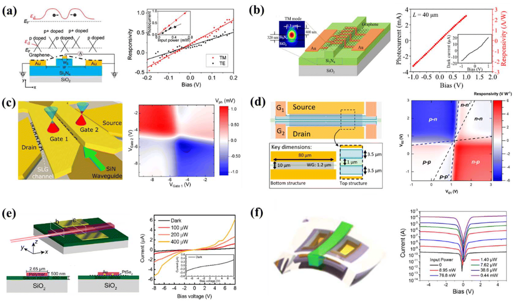 | ||
| Fig. 6 IR photodetector integrated with different waveguide and semiconductor materials. (a) Si3N4–graphene hybrid waveguide photodetector with a signal electrode with a width of wS and channel width w. The top is the energy band diagram of the photodetector under zero bias and the right is the plot of responsivity as a function of reverse bias at 1550 nm. Reproduced with permission from ref. 113. Copyright 2018, Optical Society of America. (b) A graphene–Si3N4 waveguide photodetector with transverse-magnetic mode distribution. The photocurrent and responsivity at an input optical power of 1.314 mW as a function of bias voltage are shown on the right. Reproduced with permission from ref. 114. Copyright 2018, AIP Publishing. (c) The single layer graphene photodetector on Si3N4 waveguide with a p–n junction. On the right is the photovoltaic map under zero bias voltage. Reproduced with permission from ref. 117. Copyright 2018, the American Chemical Society. (d) The double single-layer graphene photothermoelectric photodetector on Si3N4 waveguide. The simulated photovoltaic map as a function of the voltage applied to the split gate is shown on the right. Reproduced with permission from ref. 118. Copyright 2020, the American Chemical Society. (e) The hybrid PtSe2–SiN photodetector. On the right is the measured I–V curve of the PtSe2 photodetector under dark and different optical powers. Reproduced with permission from ref. 64. Copyright 2020, the American Chemical Society. (f) The flexible waveguide-integrated chalcogenide glass photodetector. The I–V curve of the photodetector under different optical powers is described on the right. Reproduced with permission from ref. 66. Copyright 2018, Optical Society of America. | ||
Due to the low light absorption rate of graphene materials, researchers have been searching for 2D materials to replace graphene.120 In 2020, Wang et al. used transition metal sulfides instead of graphene to design and fabricate MSM photodetectors integrating PtSe2 and Si3N4 waveguides,64 as shown in Fig. 6e. In this design, the researchers innovatively covered PtSe2 with a low-refractive-index polymer. Due to the combined effect of the high-refractive-index Si3N4 waveguide and the low-refractive-index polymer waveguide to form bound states in the continuum (BIC),121,122 the waveguide transmits light into the 2D material and is bound to it, thereby enhancing the mode overlap between the waveguide evanescent field and the 2D material. Consequently, the responsivity of this photodetector at 8 V bias voltage and 1550 nm is ∼12 mA W−1. In addition, optical impulse response measurements show a 3 dB bandwidth of 35 GHz, demonstrating the promise of this photodetector integrating Si3N4 waveguides and 2D materials for high-speed optoelectronic devices. Hard waveguides such as Si waveguides and Si3N4 waveguides are difficult to apply in the fields of wearable devices, flexible consumer electronics, and bendable and stretchable devices. Thus, to overcome the above-mentioned problems, the design and fabrication of flexible waveguides have received increasing attention. In 2017, Li et al. designed and fabricated an MSM photodetector based on flexible chalcogenide glass (ChG) waveguides and InGaAs,66 as depicted in Fig. 6f. Consequently, the photodetector exhibited a record optical and mechanical performance measured at 1530 nm with noise equivalent power as low as 0.02 pW Hz1/2, linear dynamic range exceeding 70 dB, and 3 dB bandwidth of GHz. In addition, the device could withstand 1000 bending cycles within a sub-millimeter radius without degrading its optoelectronic response. Therefore, the photodetector is expected to become an important device in novel bio-integrated optoelectronic systems, wearable sensors, and flexible consumer electronics.
3.2 Waveguide-integrated VIS photodetectors
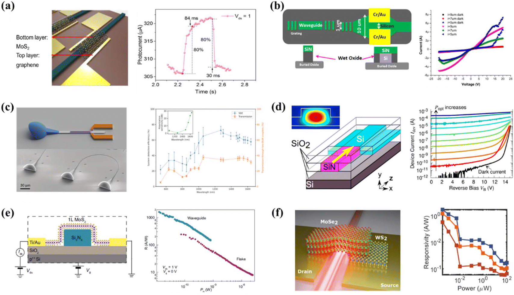
VIS light is a common and interesting wavelength band that can be used in biomedical and short-range communication applications.129,130 VIS photodetectors also play a significant role in these applications.131 The Si3N4 material has good transmittance for the VIS band, and is one of the better candidates as a VIS light waveguide.124 However, most of the research on photodetectors based on photonic platforms has focused on the IR telecommunication band, and there is still relatively little research on integrated waveguides and semiconductor materials for VIS photodetectors.Wu et al.123 reported the fabrication of a photodetector based on an Si3N4 waveguide. The photodetector integrates the current hot transfer graphene/MoS2 heterostructure (where the monolayer MoS2 is obtained by the CVD method). As shown in Fig. 7a, in this structure, photogenerated electron–hole pairs will be generated, and the heterostructure interface will rapidly separate the photogenerated electron–hole pairs. Subsequently, electron transfer to the graphene layer is induced by the built-in electric field. The Fermi energy level of the graphene layer changes in response to the back-gate voltage, which enables the device to achieve an optical responsivity of 440 mA W−1 and a rise/fall time of 80/30 ms at 532 nm. This photodetector integrating an optical waveguide with a 2D heterostructure has great potential for future applications in integrated optoelectronic circuits. Selvaraja et al.124 also reported a photodetector integrated on a planar oxide-free Si3N4 waveguide SOI platform, which was capable of detecting in the VIS to near-IR wavelength range, which has potential for applications such as biosensing and short-range communication. This is an MSM photodetector with the advantages of high responsivity, low capacitance, low dark current, and high operating speed, as shown in Fig. 7b. The photodetector integrating an Si3N4 waveguide with Si can be used in communication applications operating at high speed, providing a fairly reliable sensitivity to the device. Traditional superconducting nanowire single-photodetectors have achieved a high detection efficiency of 98% at a wavelength of 1550 nm, while superconducting nanowire single-photodetectors with integrated waveguides can achieve higher absorption efficiency due to the photons being absorbed in the traveling wave along the propagation direction. As shown in Fig. 7c, Schuck et al.125 demonstrated a single photodetector of superconducting nanowires integrated with a single Si3N4 waveguide. These researchers integrated a U-shaped superconducting nanowire single-photodetector on top of Si3N4. When connected to a fiber via a 3D coupler, absorption in a wide band range from 532 to 1640 nm can be achieved with detection efficiencies as high as 22–73%.
 | ||
| Fig. 7 VIS photodetector integrating Si3N4 waveguide with 2D materials. (a) A photodetector with integrated Si3N4 waveguide and graphene/MoS2 heterojunction. The rise/fall time of 80/30 ms at 532 nm is displayed on the right. Reproduced with permission from ref. 123. Copyright 2019, Wiley-VCH. (b) A photodetector with integrated Si3N4 waveguide and SOI platform. Photocurrent as a function of voltage is shown on the right. Reproduced with permission from ref. 124. Copyright 2018, SPIE. (c) A photodetector with integrated Si3N4 waveguide and nanowires. The right shows the detection efficiencies under different wavelengths. Reproduced with permission from ref. 125. Copyright 2021, AIP Publishing. (d) An avalanche photodetector with integrated Si3N4 and Si waveguide. The device current as a function of the reverse bias is shown on the right. Reproduced with permission from ref. 126. Copyright 2021, Springer Nature. (e) VIS photodetector-integrated Si3N4 waveguide with 2D MoS2. The right shows the responsivity under different optical power density with applied bias. Reproduced with permission from ref. 127. Copyright 2019, Published in partnership with FCT NOVA with the support of E-MRS. (f) A VIS photodetector integrated Si3N4 waveguide with the MoSe2/WS2 heterojunction photodiode. The measured responsivity as optical power density is shown on the right. Reproduced with permission from ref. 128. Copyright 2023, under Creative Commons Attribution 4.0 International License. | ||
Avalanche photodetectors capable of achieving an integrated photonic platform at VIS wavelengths can be used in a variety of miniaturized devices, such as biomedical and underwater imaging, and molecular sensing.132–134 Leong et al.126 reported the first monolithic avalanche photodetector based on a doped Si ridge waveguide with an integrated Si3N4 waveguide. As shown in Fig. 7d, the Si3N4 waveguide is used as the input waveguide to reduce the propagation loss of the device in detecting VIS light. The photodetector is capable of detecting 685 nm light at a reverse bias voltage of 20 V. The dark current of all devices can be below 70 pA at a bias voltage of 2 V, indicating that the device is prepared in a quit stable process. In addition, the photodetectors exhibit a dark current of only 1 pA when the waveguide width is 900 nm. Marin et al.127 achieved not only a VIS band photodetector integrating an Si3N4 waveguide with 2D MoS2, but also effective light absorption and photocurrent generation. Fig. 7e displays the structure of this device. The device demonstrates a different approach from conventional vertical light absorption, with 647 nm VIS light exhibiting near-transverse absorption in the device, which very effectively improves the optical response with an on–off current ratio as high as 6 × 10³. Besides, the combination of MoS2 and hexagonal boron nitride improves the detection speed of the photodetector with a rise/fall time of 13/11 s. Gherabli et al.128 constructed a VIS photodetector integrating an Si3N4 waveguide with MoSe2/WS2 heterojunction photodiode, as shown in Fig. 7f, which exhibits a high responsivity of 1 A W−1 at the VIS wavelength of 780 nm. Additionally, the dark current of the device is even reduced to below 50 pA, and the power spectral density of the dark current is as low as ∼1 × 10⁻¹² A Hz−0.5. This research can lay a certain experimental foundation for photodetectors with integrated waveguides and 2D materials in various fields such as optical communication, quantum photonics, and biochemical sensing.
3.3 Waveguide-integrated UV photodetectors
At present, UV photodetectors, as an important part of photodetectors, are mainly used in the military,135 environmental monitoring,136 medical field,137 and space.138 Due to the short wavelength of UV light, semiconductor materials with a wide bandgap or ultra-wide bandgap are generally required to realize detection, such as ZnO,139 Ga2O3,140 BN,141 AlN,142 and diamond.143 Similarly, to improve the performance of UV photodetectors, integrating UV light-transmitting waveguides with photosensitive semiconductor materials is a promising alternative. However, due to the large photon energy of UV light and the large scattering of UV light, considering the bandgap of the material, there are few waveguide materials that can transmit UV light. Therefore, the current research on UV waveguides is relatively scarce, mainly focusing on waveguide materials such as AlN,144 Si3N4,145 and ZnO.146 Consequently, there are currently fewer studies on UV photodetectors integrating UV optical waveguides with semiconductor materials. In 2001, Ivankov et al.147 designed and fabricated a UV photodetector integrating Eu3+-doped zinc borate glass (ZBG) fibers and Si, as shown in Fig. 8a. The detection principle of the photodetector is to convert the incident UV light into VIS light with a wavelength of 613 nm through the Eu3+ doped ZBG fiber. In addition, the device detects UV light through the sensing of VIS light by an Si photodiode. Consequently, the photodetector achieved a photoresponsivity of 3 mA W−1 in the UVC band with low power consumption. Further, the maximum sensitivity wavelength of this UV photodetector is in the deep UV range (240–270 nm). It is worth noting that the reason why 3D semiconductor materials are used as sensitive materials for UV photodetectors is that there are relatively few research groups studying photodetectors integrating UV waveguides and semiconductor materials, and these research groups may not have studied 2D or quasi-2D UV semiconductor materials. Considering that the fiber is relatively difficult to fix, in 2018, Maurya et al.148 designed and fabricated a vertically grown ZnO nanorod waveguide photodetector based on partially embedded anodized aluminum templates, as shown in Fig. 8b. Compared with bare ZnO nanorods, the photodetector integrating the ZnO nanorod waveguide with hybrid anodized aluminum showed a higher response in the UV band. Consequently, the UV photodetector exhibited a fast response under 365 nm light irradiation, with rise and fall times of ∼31 ms and ∼85 ms, respectively. In 2020, Floyd et al.33 designed and fabricated a UVC waveguide photodetector integrating an n-type Al0.65Ga0.35N waveguide and AlxGa1−xN multiple quantum wells, as depicted in Fig. 8c. The multifunctional photodetector can be used as both a photodetector and a light-emitting diode. Interestingly, the emitter, photodetector, and waveguide share a common epitaxial layer structure. Besides, ∼80% of the transmitted light is confined in the n+-Al0.65Ga0.35N layer, 7% in the AlN cladding, and the remaining 13% in the sapphire substrate. Consequently, the responsivity of this photodetector peaked at 250 nm (1 mA W−1).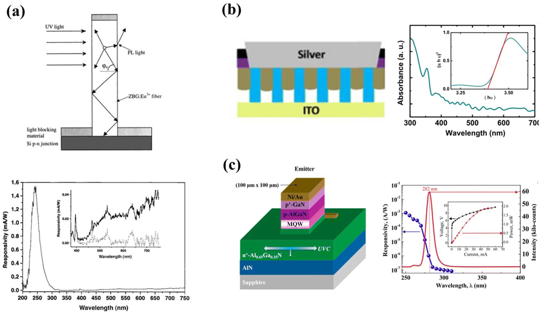 | ||
| Fig. 8 UV photodetector integrated with different waveguide and semiconductor materials. (a) Eu3+-doped waveguide photodetector with an Si p–n junction. On the right is the spectral photoresponse of the photodetector from UV to IR. Reproduced with permission from ref. 147. Copyright 2001, Wiley-VCH. (b) A vertically grown ZnO nanorod waveguide photodetector based on partially embedded anodized aluminum (AAO) templates. The absorbance curve of ZnO deposited in the AAO template is shown on the right. Reproduced with permission from ref. 148. Copyright 2018, IOP Publishing Ltd. (c) A UVC waveguide photodetector integrating n-type Al0.65Ga0.35N waveguide. On the right is the photodetector and emitter responsivity and emitted power as a function of wavelength. Reproduced with permission from ref. 33. Copyright 2020, the Japan Society of Applied Physics. | ||
4. Conclusion and outlook
Herein, we reviewed the recent studies on photodetectors with integrated waveguides and semiconductor materials for wavelength bands from the UV to IR region and discussed their potential applications. These applications mainly include optical communications, optical computing, and sensing, as summarized in Fig. 9. With the recent development, the introduction of some semiconductor materials provides alternative opportunities to achieve various active photodetectors on Si substrates because of their fascinating optoelectronic properties. Further, when waveguides and semiconductor materials are integrated, the effect of the light–matter interaction is considerably improved, thereby greatly enhancing the optoelectronic performance of photodetectors. With the rapid development of waveguide technologies, novel and high-performance photodetectors integrating waveguides with semiconductor materials will play an important role in future photoelectric applications. At present, numerous high-speed and high-responsivity waveguide/semiconductor photodetectors have been demonstrated to benefit from the special photoelectric properties of semiconductor materials. However, there are many challenges and bottlenecks preventing the fabrication of higher-performance photodetectors with integrated waveguides and semiconductor materials. Firstly, some 2D materials affect the response of photodetectors integrating waveguides and 2D material due to their shortcomings. For example, graphene materials have low absorptivity and other semiconductor materials such as MoS2 have low carrier mobility.23 As shown in Fig. 9, the performance of photodetectors integrating waveguides and semiconductors can be optimized by developing new semiconductor materials or new material structures. Recently, Flöry et al.60 reported the fabrication of stacked vdW heterostructure photodetector integrating a waveguide and graphene–MoTe2, whose photo-dark-current ratio is almost one order of magnitude better than that of a pure graphene photodetector. In addition, we can design and prepare surface plasmon structures to promote the absorption of incident light transmitted through waveguides by semiconductors, thereby improving the response of photodetectors. Moreover, heterostructures (such as p–n junctions, n–n junctions, and p–i–n junctions) can reduce the dark current and accelerate the separation of photogenerated carriers due to the presence of potential barriers and built-in electric fields, helping to realize high-performance waveguide-integrated photodetectors. Secondly, currently there is no relevant report on UV photodetectors integrating waveguides with quasi-2D or 2D semiconductor materials. A potential solution is to integrate quasi-2D β-Ga2O3 or 2D h-BN because these materials have ultra-wide bandgaps suitable for solar blind detection and vacuum UV detection.155–159 Thirdly, it is also still challenging to realize photodetector arrays integrating waveguides and semiconductor materials with high yield and throughput.96,160 Searching for advanced growth processes, for example, using the MOCVD method to grow high-quality semiconductor materials, may be the most straightforward way to solve the above-mentioned problem. Lastly, wearable systems are very important for human health, while flexible photodetectors integrating waveguides with semiconductor materials are rarely reported. It is a promising way to fabricate high-performance organic waveguides matched with semiconductor materials by using advanced preparation techniques.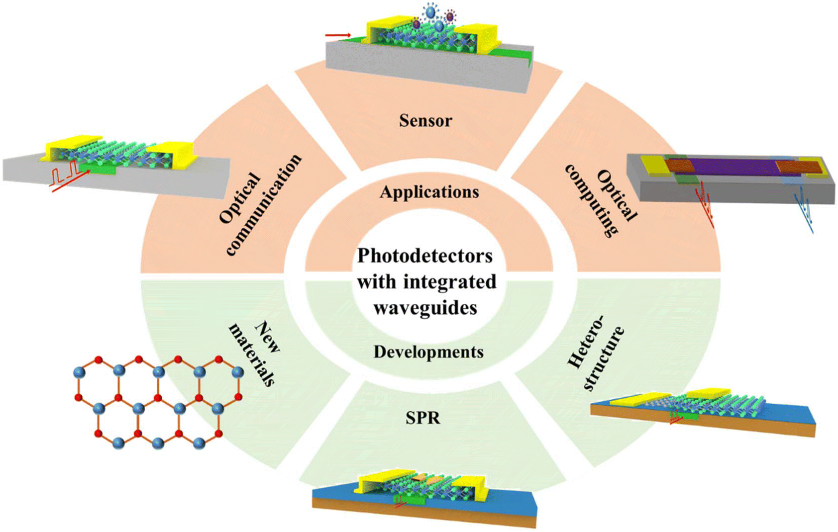 | ||
| Fig. 9 Schematic summary of the application fields and further development strategies of photodetectors with integrated waveguides. | ||
In summary, it is becoming very promising to develop photodetectors on Si substrates through integrated waveguide and semiconductor materials, which can not only compensate for the defects of silicon itself but also realize the design and fabrication of high-performance photodetectors. More importantly, when waveguides and semiconductor materials are integrated, the light–matter interaction can be greatly enhanced, resulting in improved responsivity of the photodetectors. With the rapid development of science and technology, we believe that more advanced photodetectors will appear on new integrated semiconductor materials and waveguide platforms for potential UV-IR applications in optical computing, communications, and biochemical sensing. Therefore, more efforts to realize on-chip photodetectors and apply them to large-scale photonic integrated circuits can be expected in the future.
Author contributions
X.-X. W. and G. Z. contributed equally. X.-X. W. took the lead in conceptualizing and writing the review article. G. Z. contributed towards organizing the summary figures and writing the article. Q.-J. Y. and C.-Y. S. participated in surveying references and organizing figures for each chapter. L. S. was involved in organizing tables and H.-L. L. was involved in supervising and reviewing of the article. All authors read through the article and approved it as the final version.Conflicts of interest
There are no conflicts to declare.Acknowledgements
This work was supported by National Key R&D Program of China (no. 2021YFB3202500), National Natural Science Foundation of China (no. 62027818, 61874034, and 11974320), and International Science and Technology Cooperation Program of Shanghai Science and Technology Innovation Action Plan (no. 21520713300).References
- A. A. Ahmed, M. Hashim, R. Abdalrheem and M. Rashid, J. Alloys Compd., 2019, 798, 300–310 CrossRef CAS.
- D. Thomson, A. Zilkie, J. E. Bowers, T. Komljenovic, G. T. Reed, L. Vivien, D. Marris-Morini, E. Cassan, L. Virot and J.-M. Fédéli, J. Opt., 2016, 18, 073003 CrossRef.
- M. A. Taubenblatt, J. Lightwave Technol., 2012, 30, 448–458 Search PubMed.
- N. Youngblood and M. Li, Nanophotonics, 2016, 6, 1205–1218 Search PubMed.
- D. Dai, Y. Yin, L. Yu, H. Wu, D. Liang, Z. Wang and L. Liu, Front. Optoelectron., 2016, 9, 436–449 CrossRef.
- A. W. Fang, H. Park, O. Cohen, R. Jones, M. J. Paniccia and J. E. Bowers, Opt. Express, 2006, 14, 9203–9210 CrossRef CAS PubMed.
- H. Park, Y.-h. Kuo, A. W. Fang, R. Jones, O. Cohen, M. J. Paniccia and J. E. Bowers, Opt. Express, 2007, 15, 13539–13546 CrossRef CAS PubMed.
- Y. Ishikawa, K. Wada, D. D. Cannon, J. Liu, H.-C. Luan and L. C. Kimerling, Appl. Phys. Lett., 2003, 82, 2044–2046 CrossRef CAS.
- S.-K. Chiu, M.-C. Li, J.-W. Ci, Y.-C. Hung, D.-S. Tsai, C.-H. Chen, L.-H. Lin, K. Watanabe, T. Taniguchi and N. Aoki, Nanotechnology, 2023, 34, 255703 CrossRef PubMed.
- Y. Wang, K. Ding, B. Sun, S.-T. Lee and J. Jie, Nano Res., 2016, 9, 72–93 CrossRef CAS.
- S. Zhuiykov, L. Hyde, Z. Hai, M. K. Akbari, E. Kat, C. Detavernier, C. Xue and H. Xu, Appl. Mater. Today, 2017, 6, 44–53 CrossRef.
- Z. Hai, M. K. Akbari, C. Xue, H. Xu, S. Depuydt and S. Zhuiykov, Sens. Actuators, B, 2017, 245, 954–962 CrossRef CAS.
- Z. Hai, M. K. Akbari, C. Xue, H. Xu, L. Hyde and S. Zhuiykov, Appl. Surf. Sci., 2017, 405, 169–177 CrossRef CAS.
- G. Huang, Y. Hao, Y. D. Jia, J. Guo and H. Zhang, J. Phys. D: Appl. Phys., 2023, 56, 113001 CrossRef.
- J. Zhu, J. Cheng, L. Zhang and Q. H. Liu, Mater. Lett., 2017, 186, 53–56 CrossRef CAS.
- S. Deckoff-Jones, H. Lin, D. Kita, H. Zheng, D. Li, W. Zhang and J. Hu, J. Opt., 2018, 20, 044004 CrossRef.
- A. Chatterjee, S. K. Sikdar and S. K. Selvaraja, Opt. Lett., 2019, 44, 1682–1685 CrossRef CAS PubMed.
- Y. Lin, Z. Yong, X. Luo, S. S. Azadeh, J. C. Mikkelsen, A. Sharma, H. Chen, J. C. Mak, P. G.-Q. Lo and W. D. Sacher, Nat. Commun., 2022, 13, 6362 CrossRef CAS PubMed.
- F. Yu, T.-C. Tzu, J. Gao, T. Fatema, K. Sun, P. Singaraju, S. M. Bowers, C. Reyes and A. Beling, IEEE J. Sel. Top. Quantum Electron., 2022, 29, 1–6 Search PubMed.
- R. B. Taylor, P. E. Burrows and S. R. Forrest, IEEE Photonics Technol. Lett., 1997, 9, 365–367 Search PubMed.
- H. Ma, J. Wu, Y. Wang, C. Zhong, Y. Ye, M. Wei, R. Yu, Y. Du, B. Tang, C. Sun, Y. Shi, C. Sun, L. Wang, H. Zhu, X. Qiao, L. Li and H. Lin, Adv. Opt. Mater., 2022, 10, 2201443 CrossRef CAS.
- C.-L. Wu, Y.-H. Lin, S.-P. Su, B.-J. Huang, C.-T. Tsai, H.-Y. Wang, Y.-C. Chi, C.-I. Wu and G.-R. Lin, ACS Photonics, 2015, 2, 1141–1154 CrossRef CAS.
- D. Yamashita, H. Machiya, K. Otsuka, A. Ishii and Y. K. Kato, APL Photonics, 2021, 6, 031302 CrossRef CAS.
- C. Li, R. Tian, X. Chen, L. Gu, Z. Luo, Q. Zhang, R. Yi, Z. Li, B. Jiang and Y. Liu, ACS Nano, 2022, 16, 20946–20955 CrossRef CAS PubMed.
- S. Zhang, Y. Liu, C. Fang, Y. Shao, G. Han, J. Zhang and Y. Hao, Superlattices Microstruct., 2018, 122, 501–509 CrossRef CAS.
- J. Jian, J. Wu, C. Zhong, H. Ma, B. Sun, Y. Ye, Y. Luo, M. Wei, K. Lei, R. Liu, Z. Chen, G. Li, H. Dai, R. Tang, C. Sun, J. Li, W. Li, M. Li, H. Lin and L. Li, ACS Photonics, 2023, 10, 3494–3501 CrossRef CAS.
- X. Li, J. Yu, S. Wageh, A. A. Al-Ghamdi and J. Xie, Small, 2016, 48, 6640–6696 CrossRef PubMed.
- Z. Lu, Y. Xu, Y. Yu, K. Xu, J. Mao, G. Xu, Y. Ma, D. Wu and J. Jie, Adv. Funct. Mater., 2020, 30, 1907951 CrossRef CAS.
- J. Wu, H. Ma, C. Zhong, M. Wei, C. Sun, Y. Ye, Y. Xu, B. Tang, Y. Luo, B. Sun, J. Jian, H. Dai, H. Lin and L. Li, Nano Lett., 2022, 22, 6816–6824 CrossRef CAS PubMed.
- Y. Gao, H. K. Tsang and C. Shu, Nanoscale, 2018, 10, 21851–21856 RSC.
- Y. Ding, Z. Cheng, X. Zhu, K. Yvind, J. Dong, M. Galili, H. Hu, N. A. Mortensen, S. Xiao and L. K. Oxenløwe, Nanophotonics, 2020, 9, 317–325 CrossRef CAS.
- J. Wu, Y. Ye, J. Jian, X. Yao, J. Li, B. Tang, H. Ma, M. Wei, W. Li, H. Lin and L. Li, Nano Lett., 2023, 23, 6440–6448 CrossRef CAS PubMed.
- R. Floyd, K. Hussain, A. Mamun, M. Gaevski, G. Simin, M. Chandrashekhar and A. Khan, Appl. Phys. Express, 2020, 13, 022003 CrossRef CAS.
- N. Youngblood, C. Chen, S. J. Koester and M. Li, Nat. Photonics, 2015, 9, 247–252 CrossRef CAS.
- R. Maiti, C. Pati, M. Saadi, T. Xie, J. Azadani, B. Uluutku, R. Amin, A. Briggs, M. Miscuglio, D. Thourhout, S. Solares, T. Low, R. Agarwal, S. Bank and V. Sorge, Nat. Photonics, 2020, 14, 578–584 CrossRef CAS.
- S. Zhu, Y. Zhang, Y. Ren, Y. Wang, K. Zhai, H. Feng, Y. Jin, Z. Lin, J. Feng, S. Li, Q. Yang, N. H. Zhu, E. Pun and C. Wang, Adv. Photonics Res., 2023, 4, 2300045 CrossRef CAS.
- K. H. Li, Y. F. Cheung, W. Y. Fu, K. K.-Y. Wong and H. W. Choi, IEEE J. Sel. Top. Quantum Electron., 2018, 24, 1–6 Search PubMed.
- R. He, N. Liu, Y. Gao, R. Chen, S. Zhang, H. Yuan, Y. Duo, J. Xu, X. Ji, J. Yan, J. Wang, J. Liu, J. Li and T. Wei, Nano Energy, 2022, 104, 107928 CrossRef CAS.
- R. Soref, Nat. Photonics, 2015, 9, 358–359 CrossRef CAS.
- Y.-C. Chen, Y.-J. Lu, C.-N. Lin, Y.-Z. Tian, C.-J. Gao, L. Dong and C.-X. Shan, J. Mater. Chem. C, 2018, 6, 5727–5732 RSC.
- W.-C. Lai, S. Chakravarty, Y. Zou and R. T. Chen, Opt. Lett., 2012, 37, 1208–1210 CrossRef CAS PubMed.
- Y. Wang, W. Yin, Q. Han, X. Yang, H. Ye, Q. Lv and D. Yin, Chin. Phys. B, 2016, 25, 118103 CrossRef.
- V. Sorianello, M. Balbi, L. Colace, G. Assanto, L. Socci, L. Bolla, G. Mutinati and M. Romagnoli, Phys. E, 2009, 41, 1090–1093 CrossRef CAS.
- J.-y. Ding, X.-s. Chen, Q. Li, W.-w. Tang, C.-l. Liu, H.-l. Zhen, Y.-l. Jing, H. Wang and W. Lu, Opt. Quantum Electron., 2015, 47, 2347–2357 CrossRef CAS.
- J. Fujikata, M. Noguchi, R. Katamawari, K. Inaba, H. Ono, D. Shimura, Y. Onawa, H. Yaegashi and Y. Ishikawa, Opt. Express, 2023, 31, 10732–10743 CrossRef CAS PubMed.
- N. Khongpetch, W. Traiwattanapong, S. Chiangga, P. Limsuwan and P. Chaisakul, IEEE Access, 2023, 11, 19458–19468 Search PubMed.
- H. Zhao, M. Feng, J. Liu, X. Sun, T. Tao, Q. Sun and H. Yang, Nanophotonics, 2023, 12, 111–118 CrossRef CAS.
- J. Zhang, Y. Li, C. Jiang and Z. Zhao, IEEE Sens. J., 2021, 21, 20099–20106 CAS.
- H. Wang, S. Jiang, L. Zhang, B. Yu, D. Chen, W. Yang and L. Qian, Nanoscale, 2018, 10, 4727–4734 RSC.
- K. S. Novoselov, A. K. Geim, S. V. Morozov, D.-e. Jiang, Y. Zhang, S. V. Dubonos, I. V. Grigorieva and A. A. Firsov, Science, 2004, 306, 666–669 CrossRef CAS PubMed.
- R. Chen, G. Liu, F. Qiu, Y. Tan and F. Chen, Opt. Mater. Express, 2022, 12, 3614–3620 CrossRef CAS.
- C. Oliveira, V. Dmitriev, G. Melo and W. Castro, Microw. Opt. Technol. Lett., 2022, 64, 1170–1175 CrossRef.
- R. Maiti, C. Patil, M. Saadi, T. Xie, J. Azadani, B. Uluutku, R. Amin, A. Briggs, M. Miscuglio and D. Van Thourhout, Nat. Photonics, 2020, 14, 578–584 CrossRef CAS.
- H. Zhao, L. Yang, W. Wu, X. Cai, F. Yang, H. Xiu, Y. Wang, Q. Zhang, X. Xin and F. Zhang, ACS Nano, 2023, 17, 7466–7474 CrossRef CAS PubMed.
- X. Li, Y. Zhu, W. Cai, M. Borysiak, B. Han, D. Chen, R. D. Piner, L. Colombo and R. S. Ruoff, Nano Lett., 2009, 9, 4359–4363 CrossRef CAS PubMed.
- R. A. Hemnani, J. P. Tischler, C. Carfano, R. Maiti, M. H. Tahersima, L. Bartels, R. Agarwal and V. J. Sorger, 2D Mater., 2018, 6, 015006 CrossRef.
- H. Yang, S. F. Yu, H. Liang, C. Pang, B. Yan and T. Yu, J. Appl. Phys., 2009, 106, 043102 CrossRef.
- D. Schall, D. Neumaier, M. Mohsin, B. Chmielak, J. Bolten, C. Porschatis, A. Prinzen, C. Matheisen, W. Kuebart, B. Junginger, W. Templ, A. Giesecke and H. Kurz, ACS Photonics, 2014, 1, 781–784 CrossRef CAS.
- R.-J. Shiue, Y. Gao, Y. Wang, C. Peng, A. D. Robertson, D. K. Efetov, S. Assefa, F. H. Koppens, J. Hone and D. Englund, Nano Lett., 2015, 15, 7288–7293 CrossRef CAS PubMed.
- N. Flöry, P. Ma, Y. Salamin, A. Emboras, T. Taniguchi, K. Watanabe, J. Leuthold and L. Novotny, Nat. Nanotechnol., 2020, 15, 118–124 CrossRef PubMed.
- Y. A. Vlasov and S. J. McNab, Opt. Express, 2004, 12, 1622–1631 CrossRef PubMed.
- S. J. Pearton, J. C. Yang, P. H. Cary, F. Ren, J. Y. Kim, M. J. Tadjer and M. A. Mastro, Appl. Phys. Rev., 2018, 5, 1 Search PubMed.
- A. V. Krasavin and A. V. Zayats, Opt. Express, 2010, 18, 11791–11799 CrossRef CAS PubMed.
- Y. Wang, Z. Yu, Z. Zhang, B. Sun, Y. Tong, J.-B. Xu, X. Sun and H. K. Tsang, ACS Photonics, 2020, 7, 2643–2649 CrossRef CAS.
- S. H. Badri and M. M. Gilarlue, Opt. Commun., 2020, 460, 125089 CrossRef CAS.
- L. Li, H. Lin, Y. Huang, R.-J. Shiue, A. Yadav, J. Li, J. Michon, D. Englund, K. Richardson and T. Gu, Optica, 2018, 5, 44–51 CrossRef.
- W. Yuan, Y. Xu, X. Gao, B. Zhu, W. Cai, G. Zhu, Y. Yang and Y. Wang, Opt. Mater. Express, 2016, 6, 2366–2373 CrossRef CAS.
- D. X. Dai, J. Bauters and J. E. Bowers, Light: Sci. Appl., 2012, 1, e1 CrossRef.
- Q. Qiu and Z. Huang, Adv. Mater., 2021, 33, 2008126 CrossRef CAS PubMed.
- G. Zeng, M.-R. Zhang, Y.-C. Chen, X.-X. Li, D.-B. Chen, C.-Y. Shi, X.-F. Zhao, N. Chen, T.-Y. Wang and D. W. Zhang, Mater. Today Phys., 2023, 33, 101042 CrossRef CAS.
- X. Gan, R.-J. Shiue, Y. Gao, I. Meric, T. F. Heinz, K. Shepard, J. Hone, S. Assefa and D. Englund, Nat. Photonics, 2013, 7, 883–887 CrossRef CAS.
- D. Schall, E. Pallecchi, G. Ducournau, V. Avramovic, M. Otto and D. Neumaier, Opt. Fiber Commun. Conf. and Expo., IEEE, 2018, pp. 1–3.
- L. Huang, B. Dong, X. Guo, Y. Chang, N. Chen, X. Huang, W. Liao, C. Zhu, H. Wang and C. Lee, ACS Nano, 2018, 13, 913–921 CrossRef PubMed.
- P. Ma, N. Flöry, Y. Salamin, A. Emboras, T. Taniguchi, K. Watanabe, L. Novotny and J. Leuthold, Conf. on Lasers and Electro-Optics, IEEE, 2019, pp. 1–2.
- Z. Ma, L. Yang, L. Liu, S. Wang and L.-M. Peng, ACS Nano, 2020, 14, 7191–7199 CrossRef CAS PubMed.
- J. Wu, M. Wei, J. Mu, H. Ma, C. Zhong, Y. Ye, C. Sun, B. Tang, L. Wang, J. Li, X. Xu, B. Liu, L. Li and H. Lin, ACS Nano, 2021, 15, 15982–15991 CrossRef CAS PubMed.
- S. M. Nawaz, M. I. Niass, Y. Wang, Z. Xing, F. Wang and Y. Liu, Superlattices Microstruct., 2020, 145, 106643 CrossRef CAS.
- L. Zhang, K. Khan, J. Zou, H. Zhang and Y. Li, Adv. Mater. Interfaces, 2019, 6, 1901329 CrossRef.
- M. Derakhshi, S. Daemi, P. Shahini, A. Habibzadeh, E. Mostafavi and A. A. Ashkarran, J. Funct. Biomater., 2022, 13, 27 CrossRef CAS PubMed.
- G. Kim, S. Song and D. Jariwala, Mater. Res. Lett., 2023, 11, 327–346 CrossRef CAS.
- E. Lacatus, Mater. Today: Proc., 2018, 5, 17484–17491 CAS.
- E. Wu, D. Wu, C. Jia, Y. Wang, H. Yuan, L. Zeng, T. Xu, Z. Shi, Y. Tian and X. Li, ACS Photonics, 2019, 6, 565–572 CrossRef CAS.
- P. Grant, S. Laframboise, R. Dudek, M. Graf, A. Bezinger and H. Liu, Electron. Lett., 2009, 45, 1 CrossRef.
- E. W. Taylor, T. Zeng, D. Wood and R. O. Claus, Enabl. Photon. Technol. Aerosp. Appl. VI, 2004, vol. 5435, pp. 164–170 Search PubMed.
- U. Varshney, N. Aggarwal and G. Gupta, J. Mater. Chem. C, 2022, 10, 1573–1593 RSC.
- X. Guo, L. Tang, J. Xiang, R. Ji, K. Zhang, S. K. Lai, J. Zhao, J. Kong and S. P. Lau, AIP Adv., 2016, 6, 055318 CrossRef.
- Z. Alaie, S. M. Nejad and M. Yousefi, Mater. Sci. Semicond. Process., 2015, 29, 16–55 CrossRef CAS.
- M.-K. Lee, C.-H. Chu, Y.-H. Wang and S. Sze, Opt. Lett., 2001, 26, 160–162 CrossRef CAS PubMed.
- J. Wang and S. Lee, Sensors, 2011, 11, 696–718 CrossRef CAS PubMed.
- P. Binetti, X. Leijtens, T. De Vries, Y. Oei, L. Di Cioccio, J.-M. Fedeli, C. Lagahe, J. Van Campenhout, D. Van Thourhout and P. Van Veldhoven, IEEE Photonics J., 2010, 2, 299–305 Search PubMed.
- F. Koppens, T. Mueller, P. Avouris, A. Ferrari, M. Vitiello and M. Polini, Nat. Nanotechnol., 2014, 9, 780–793 CrossRef CAS PubMed.
- M. Freitag, T. Low, F. Xia and P. Avouris, Nat. Photonics, 2013, 7, 53–59 CrossRef CAS.
- X. Xu, N. M. Gabor, J. S. Alden, A. M. Van Der Zande and P. L. McEuen, Nano Lett., 2010, 10, 562–566 CrossRef CAS PubMed.
- E. C. Peters, E. J. Lee, M. Burghard and K. Kern, Appl. Phys. Lett., 2010, 97, 193102 CrossRef.
- Z. Chen, Z. Cheng, J. Wang, X. Wan, C. Shu, H. K. Tsang, H. P. Ho and J. B. Xu, Adv. Opt. Mater., 2015, 3, 1207–1214 CrossRef CAS.
- J. Li, C. Liu, H. Chen, J. Guo, M. Zhang and D. Dai, Nanophotonics, 2020, 9, 2295–2314 CrossRef CAS.
- N. Ilyas, D. Li, Y. Song, H. Zhong, Y. Jiang and W. Li, Sensors, 2018, 18, 4163 CrossRef PubMed.
- A. K. Dutta, R. Olah, G. Mizuno and N. K. Dhar, Opt. Metro Netw. Short-Haul Syst. III, 2011, vol. 7959, p. 795906 Search PubMed.
- Q. Wang, Y. Zhang and Z. Wei, Chin. J. Chem., 2023, 41, 958–978 CrossRef CAS.
- J. Miao, B. Song, Z. Xu, L. Cai, S. Zhang, L. Dong and C. Wang, Small, 2018, 14, 1702082 CrossRef PubMed.
- H. Schneider, P. Koidl, M. Walther, J. Fleißner and J. Ziegler, TM, Tech. Mess., 1999, 66, 344–349 CrossRef CAS.
- M. Fauci, R. Breiter, W. Cabanski, W. Fick, R. Koch, J. Ziegler and S. Gunapala, Infrared Phys. Technol., 2001, 42, 337–344 CrossRef.
- Y. Zhang, L. Tang and K. S. Teng, Nanotechnology, 2020, 31, 304002 CrossRef CAS PubMed.
- J. Wang, Z. Cheng, Z. Chen, X. Wan, B. Zhu, H. K. Tsang, C. Shu and J. Xu, Nanoscale, 2016, 8, 13206–13211 RSC.
- A. Pospischil, M. Humer, M. M. Furchi, D. Bachmann, R. Guider, T. Fromherz and T. Mueller, Nat. Photonics, 2013, 7, 892–896 CrossRef CAS.
- Y. Ma, Y. Chang, B. Dong, J. Wei, W. Liu and C. Lee, ACS Nano, 2021, 15, 10084–10094 CrossRef CAS PubMed.
- Y.-Q. Bie, G. Grosso, M. Heuck, M. M. Furchi, Y. Cao, J. Zheng, D. Bunandar, E. Navarro-Moratalla, L. Zhou and D. K. Efetov, Nat. Nanotechnol., 2017, 12, 1124–1129 CrossRef CAS PubMed.
- J. Guo, J. Li, C. Liu, Y. Yin, W. Wang, Z. Ni, Z. Fu, H. Yu, Y. Xu and Y. Shi, Light: Sci. Appl., 2020, 9, 29 CrossRef CAS PubMed.
- L. Li, Y. Yu, G. J. Ye, Q. Ge, X. Ou, H. Wu, D. Feng, X. H. Chen and Y. Zhang, Nat. Nanotechnol., 2014, 9, 372–377 CrossRef CAS PubMed.
- H. Liu, A. T. Neal, Z. Zhu, Z. Luo, X. Xu, D. Tománek and P. D. Ye, ACS Nano, 2014, 8, 4033–4041 CrossRef CAS PubMed.
- M. Liu, X. Yin, E. Ulin-Avila, B. Geng, T. Zentgraf, L. Ju, F. Wang and X. Zhang, Nature, 2011, 474, 64–67 CrossRef CAS PubMed.
- D. Dai and J. E. Bowers, Nanophotonics, 2014, 3, 283–311 CAS.
- Y. Gao, G. Zhou, N. Zhao, H. K. Tsang and C. Shu, Opt. Lett., 2018, 43, 1399–1402 CrossRef CAS PubMed.
- Y. Gao, L. Tao, H. K. Tsang and C. Shu, Appl. Phys. Lett., 2018, 112, 211107 CrossRef.
- S. D. Sarma, S. Adam, E. Hwang and E. Rossi, Rev. Mod. Phys., 2011, 83, 407 CrossRef.
- X. Wang, Z. Cheng, K. Xu, H. K. Tsang and J.-B. Xu, Nat. Photonics, 2013, 7, 888–891 CrossRef CAS.
- J. E. Muench, A. Ruocco, M. A. Giambra, V. Miseikis, D. Zhang, J. Wang, H. F. Watson, G. C. Park, S. Akhavan and V. Sorianello, Nano Lett., 2019, 19, 7632–7644 CrossRef CAS PubMed.
- V. Mišeikis, S. Marconi, M. A. Giambra, A. Montanaro, L. Martini, F. Fabbri, S. Pezzini, G. Piccinini, S. Forti and B. Terrés, ACS Nano, 2020, 14, 11190–11204 CrossRef PubMed.
- N. M. Gabor, J. C. Song, Q. Ma, N. L. Nair, T. Taychatanapat, K. Watanabe, T. Taniguchi, L. S. Levitov and P. Jarillo-Herrero, Science, 2011, 334, 648–652 CrossRef CAS PubMed.
- T. Zhu, Y. Zhang, X. Wei, M. Jiang and H. Xu, Front. Phys., 2023, 18, 33601 CrossRef.
- Z. Yu, X. Xi, J. Ma, H. K. Tsang, C.-L. Zou and X. Sun, Optica, 2019, 6, 1342–1348 CrossRef CAS.
- Z. Yu and X. Sun, Light: Sci. Appl., 2020, 9, 1 CrossRef CAS PubMed.
- Z. Wu, T. Zhang, Y. Chen, Y. Zhang and S. Yu, Phys. Status Solidi RRL, 2019, 13, 1800338 CrossRef.
- A. Chatterjee and S. K. Selvaraja, Opt. Compon. Mater. XV, 2018, vol. 10528, pp. 160–165 Search PubMed.
- M. A. Wolff, F. Beutel, J. Schütte, H. Gehring, M. Häußler, W. Pernice and C. Schuck, Appl. Phys. Lett., 2021, 118, 154004 CrossRef CAS.
- S. Yanikgonul, V. Leong, J. R. Ong, T. Hu, S. Y. Siew, C. E. Png and L. Krivitsky, Nat. Commun., 2021, 12, 1834 CrossRef CAS PubMed.
- J. G. Marin, D. Unuchek, K. Watanabe, T. Taniguchi and A. Kis, npj 2D Mater. Appl., 2019, 3, 14 CrossRef.
- R. Gherabli, S. Indukuri, R. Zektzer, C. Frydendahl and U. Levy, Light: Sci. Appl., 2023, 12, 60 CrossRef CAS PubMed.
- T. Komine and M. Nakagawa, IEEE Trans. Consum. Electron., 2004, 50, 100–107 CrossRef.
- X. Shu, L. Beckmann and H. F. Zhang, J. Biomed. Opt., 2017, 22, 121707–121707 Search PubMed.
- H. Zhang, D. Wei, X. Song, Z. Xu, F. Wang, H. Li, W. Sun, Z. Dai, Y. Ren and Y. Ye, Nanotechnology, 2023, 34, 185205 CrossRef PubMed.
- V. Gruev, J. Van der Spiegel and N. Engheta, Opt. Express, 2010, 18, 19292–19303 CrossRef CAS PubMed.
- J. Miao and C. Wang, Nano Res., 2021, 14, 1878–1888 CrossRef.
- Y. Yuan, B. Tossoun, Z. Huang, X. Zeng, G. Kurczveil, M. Fiorentino, D. Liang and R. G. Beausoleil, J. Semicond., 2022, 43, 021301 CrossRef CAS.
- J. Yang, K. Liu, X. Chen and D. Shen, Prog. Quantum Electron., 2022, 83, 100397 CrossRef.
- G. Shang, L. Tang, G. Wu, S. Yuan, M. Jia, X. Guo, X. Zheng, W. Wang, B. Yue and K. S. Teng, Sensors, 2023, 23, 2741 CrossRef CAS PubMed.
- Y. Liu, Z. C. Li, P. F. Wang, F. Huang and J. L. Sun, J. Infrared Millimeter Waves, 2023, 42, 169–187 CAS.
- E. Monroy, F. Omnès and F. Calle, Semicond. Sci. Technol., 2003, 18, R33 CrossRef CAS.
- J. Hu, J. Chen, T. Ma and Z. Li, Nanotechnology, 2023, 34, 232002 CrossRef PubMed.
- L. Qu, J. Ji, X. Liu, Z. Shao, M. Cui, Y. Zhang, Z. Fu, Y. Huang, G. Yang and W. Feng, Nanotechnology, 2023, 34, 225203 CrossRef PubMed.
- N. R. Abdullah, B. J. Abdullah, C.-S. Tang and V. Gudmundsson, Mater. Sci. Eng., B, 2023, 288, 116147 CrossRef CAS.
- T. Li, Y. Lu and Z. Chen, Nanomaterials, 2022, 12, 4169 CrossRef CAS PubMed.
- M. Feng, P. Jin, X. Meng, P. Xu, X. Huo, G. Zhou, P. Qu, J. Wu and Z. Wang, J. Phys. D: Appl. Phys., 2022, 55, 404005 CrossRef CAS.
- M. M. Satter, Z. Lochner, T.-T. Kao, Y.-S. Liu, X.-H. Li, S.-C. Shen, R. D. Dupuis and P. D. Yoder, IEEE J. Quantum Electron., 2014, 50, 166–173 CAS.
- A. Z. Subramanian, E. Ryckeboer, A. Dhakal, F. Peyskens, A. Malik, B. Kuyken, H. Zhao, S. Pathak, A. Ruocco and A. De Groote, Photonics Res., 2015, 3, B47–B59 CrossRef CAS.
- E. S. Leong, S. F. Yu, A. Abiyasa and S. P. Lau, Appl. Phys. Lett., 2006, 88, 091116 CrossRef.
- A. Ivankov and W. Bauhofer, Phys. Status Solidi A, 2001, 185, 145–151 CrossRef CAS.
- M. R. Maurya and V. Toutam, Nanotechnology, 2018, 30, 085704 CrossRef PubMed.
- N. Youngblood, Y. Anugrah, R. Ma, S. J. Koester and M. Li, Nano Lett., 2014, 14, 2741–2746 CrossRef CAS PubMed.
- S. Schuler, D. Schall, D. Neumaier, L. Dobusch, O. Bethge, B. Schwarz, M. Krall and T. Mueller, Nano Lett., 2016, 16, 7107–7112 CrossRef CAS PubMed.
- D. Schall, C. Porschatis, M. Otto and D. Neumaier, J. Phys. D: Appl. Phys., 2017, 50, 124004 CrossRef.
- Y. Ding, Z. Cheng, X. Zhu, K. Yvind, J. Dong, M. Galili, H. Hu, N. A. Mortensen, S. Xiao and L. K. Oxenløwe, Nanophotonics, 2020, 9, 317–325 CrossRef CAS.
- C. Chen, N. Youngblood, R. Peng, D. Yoo, D. A. Mohr, T. W. Johnson, S.-H. Oh and M. Li, Nano Lett., 2017, 17, 985–991 CrossRef CAS PubMed.
- Y. Yin, R. Cao, J. Guo, C. Liu, J. Li, X. Feng, H. Wang, W. Du, A. Qadir and H. Zhang, Laser Photonics Rev., 2019, 13, 1900032 CrossRef.
- S. Pu, Y. Ou, M. Cai, Y. Xia and Z. Wu, Mater. Lett., 2023, 342, 134283 CrossRef CAS.
- Y.-C. Lu, Z.-F. Zhang, X. Yang, G.-H. He, C.-N. Lin, X.-X. Chen, J.-H. Zang, W.-B. Zhao, Y.-C. Chen and L.-L. Zhang, Nano Res., 2022, 15, 7631–7638 CrossRef CAS.
- C. Zhang, K. Liu, Q. Ai, X. Huang, X. Chen, Y. Zhu, J. Yang, Z. Cheng, B. Li and L. Liu, J. Phys. Chem. C, 2022, 126, 21839–21846 CrossRef CAS.
- W. Zheng, R. Lin, Z. Zhang and F. Huang, ACS Appl. Mater. Interfaces, 2018, 10, 27116–27123 CrossRef CAS PubMed.
- Y. Li, J. Guo, W. Zheng and F. Huang, Appl. Phys. Lett., 2020, 117, 023504 CrossRef CAS.
- Y. Liu, Y. Huang and X. Duan, Nature, 2019, 567, 323–333 CrossRef CAS PubMed.
| This journal is © The Royal Society of Chemistry 2024 |