
 Open Access Article
 This Open Access Article is licensed under a
 Creative Commons Attribution 3.0 Unported Licence
Rational design of comb-like 1D–1D ZnO–ZnSe heterostructures toward their excellent performance in flexible photodetectors†
Ming-Jin
Liu‡
abc,
Hsuan-Chu
Chen‡
abc,
Tse-Ning
Yang
a,
Shu-Chi
Wu
abc,
Yao-Jen
Kuo
abc,
Ruei-Hong
Cyu
abc,
Yu-Ren
Peng
abc and
Yu-Lun
Chueh
 *abcd
*abcd
aDepartment of Materials Science and Engineering, National Tsing-Hua University, 30013, Taiwan. E-mail: ylchueh@mx.nthu.edu.tw
bCollege of Semiconductor Research, National Tsing-Hua University, Hsinchu, 30013, Taiwan
cDepartment of Physics, National Sun Yat-Sen University, Kaohsiung, 80424, Taiwan
dDepartment of Materials Science and Engineering, Korea University, Seoul 02841, Republic of Korea
First published on 20th April 2024
Abstract
One-dimensional (1D) Zn-based heterostructures have attracted considerable interest in the field of photodetection because of their tunable properties, flexibility, and unique optoelectronic properties. However, designing 1D multi-component Zn-based heterostructures for advanced photodetectors is still a great challenge. Herein, comb-like 1D–1D ZnO–ZnSe heterostructures with ZnO and ZnSe nanowires (NWs) comprising the shaft and teeth of a comb are reported. The length of the ZnO NWs can be modulated in the range of 300–1200 nm. Microstructural characterizations confirm that the 1D heterostructure clearly shows the spatial distribution of individual components. The well-designed structure displays an extended broadband photoresponse and higher photosensitivity than pure ZnSe NWs. Furthermore, ZnSe NWs with an appropriate length of ZnO branches show increased photoresponses of 3835% and 798% compared to those of pure ZnSe NWs under green and red-light irradiation, respectively. In addition, the integrated flexible photodetector presents excellent folding endurance after 1000 bending tests. This well-designed structure has significant potential for other 1D-based semiconductors in optoelectronic applications.
Introduction
One-dimensional ZnX (X = O, S, Se, and Te) nanostructures have been extensively applied in the field of photodetection owing to their high chemical stability and excellent optoelectronic properties.1 For example, 1D ZnO and ZnS showed a high UV photoresponse with a fast response time.2 In particular, 1D ZnSe showed high potential for blue/UV photodetectors with high spectral selectivity and a fast response time.3 However, a single-component 1D ZnX photodetector showed unsatisfactory photodetection performance because of the intrinsic defects (O/S/Se vacancies and Zn interstitials) and a narrow photoresponse spectrum.3–7 Several strategies, such as heteroatom doping,8–12 construction of heterostructures,13–15 and regulation of morphology,16,17 have been developed to improve the performance of photodetection. Among them, the construction of a multi-component ZnX heterostructure is considered a facile and efficient method to regulate the performance of photodetection. For example, Mu et al. synthesized a 1D ZnSSe–ZnSe axial heterostructure using temperature-controlled chemical vapor deposition.13 The designed structure showed a fast response time (23 ms), high responsivity (R = 6.3 × 10⁵ A W−1), and external quantum efficiency (EQE = 2.08 × 10⁶), which are higher than those of single-component ZnSe nanowires (NWs) (R = 4.2 × 10⁵ A W−1 and EQE = 1.3 × 10⁶).13 The improved performance may be ascribed to the built-in electric field of the heterojunction, resulting in the effective separation and transfer of photogenerated carriers. Highly crystallized ZnS–ZnO biaxial nanobelts exhibited high spectral selectivity and a broadband photoresponse in the UV band.18 Similarly, highly crystallized 1D ZnS–ZnO branched nanostructures showed an enhanced photoresponse compared to pure ZnO and ZnSe nanostructures.19 These examples provide a possible method for regulating the morphology of 1D Zn-based semiconductors to enhance photodetection performance. However, for 1D Zn-based photodetectors, controllable growth is still a great challenge in the application of high-performance flexible photodetectors. In particular, one component of heterostructures should have an appropriate density or thickness to obtain high photoabsorption.In this study, a two-step thermal evaporation method, combined with a modified vapor–solid–liquid (VLS) strategy, was employed for the preparation of a comb-like 1D–1D ZnO–ZnSe heterostructure with a controllable length of 1D ZnO. To investigate the flexible photodetection capability of the ZnO–ZnSe heterostructure, the heterostructure and Ag NW transparent electrodes were combined to fabricate flexible photodetectors using a cost-effective printing method. This heterojunction exhibited extended and improved photodetection compared to pure ZnSe NWs. An appropriate length of ZnO NWs of the as-prepared heterostructures showed an excellent response toward blue and green light at room temperature. In addition, the device exhibited superior folding endurance after 1000 bending tests.
Experimental
Synthesis of 1D ZnSe NWs
ZnSe NWs were synthesized using a horizontal double-tube system. First, a p-type Si (100) substrate was coated with a 3 nm-Au film by electron beam evaporation technique and then annealed at 600 °C with an Ar gas flow rate of 100 sccm. Subsequently, the Si substrate coated with the Au film was placed 10 cm away from ZnSe powders (20 mg, Alfa Aesar, 99.999%) and downstream of the flowing gas. The ZnSe powders were placed in a high-temperature zone (900 °C), whereas the Si substrate is in a low-temperature zone (600 °C). During the growth process, the pressure was maintained at 5–40 torr with an Ar gas flow rate of 60 sccm for 30 min.Synthesis of the 1D ZnO–ZnSe comb-like structure
In a typical process, as shown in Fig. S1,† 120 mg of Zn powder (Alfa Aesar, 99.999%) was placed on the windward side of a quartz boat. The Si substrate covered with the prepared ZnSe NWs was then placed downwind of the growth of ZnO branches. To avoid rapid vaporization of the Zn powder, a 15 × 20 mm blank glass was used as a cover on top of the powder. A quartz boat was placed at the center of the heating zone with an Ar/0.5% O2 gas mixture flow rate of 50 sccm. The length of ZnO could be controlled by the pressure of the tube and growth time. For example, at a constant pressure (20 torr), ZnO NWs with short (∼300 nm), medium (∼600 nm) and long lengths (∼1000 nm) were obtained at 20, 30, and 40 min, respectively. In the same growth time (30 min), ZnO NWs with short (∼250 nm), medium (∼600 nm) and long lengths (∼1200 nm) were obtained at 5, 20 and 40 torr, respectively.Material characterization
The elemental compositions and morphologies were analyzed using transmission electron microscopy (TEM; JEOL, JEM-3000F FEGTEM, 300 kV) equipped with energy-dispersive spectroscopy (EDS; INCA, Oxford Instruments). Cold-field emission scanning electron microscopy (SEM; Hitachi SU8010) was used to examine the morphologies of the as-prepared materials. X-ray diffraction (XRD) analyses were conducted using a Shimadzu XRD-6000 X-ray spectrometer under irradiation of mono-chromatic Cu-Kα radiation (λ ∼ 1.54 Å) with a accelerating voltage of 30 kV, a tube current of 20 mA and a scanning step of 0.02°. Raman spectra were obtained using a Horiba Jobin Yvon LabRAM HR 800 Raman spectrometer and PL spectra of the ZnSe NWs and ZnO–ZnSe heterostructures were obtained by using a He–Cd laser with a wavelength of 325 nm. The photoresponse and sheet resistance were measured using a Keithley 4200-SCS semiconductor characterization system.Device fabrication and measurements
Transparent polyimide (PI) substrates, purchased from Taichung Tech. Inc., were selected as flexible and transparent substrates. The PI substrates were cut into 12 × 12 cm pieces and cleaned with acetone, isopropanol (IPA), and deionized water for 15 min each. Then, 50 μm-thick polydimethylsiloxane (PDMS) was coated on a PI substrate and baked at 85 °C for 5 h. Fig. S6† shows a schematic of the fabrication process for all-nanowire devices. First, ZnO–ZnSe heterostructure NWs were transferred from Si substrates to PI/PDMS substrates via contact printing method. A pressure of approximately 500 g cm−2 was applied to the Si substrates. Second, the PI substrate was covered with a metallic hard mask. Subsequently, Ag NW transparent electrodes (TEs) were prepared using a fast-moving cylindrical blade coating method. A commercial blade coating machine with a step motor was used (Fig. S7†). The PI substrate with a thin layer of PDMS (∼50 μm) was placed on the coating machine and baked at 50 °C. The distance between the blade and substrate was 100 μm. Furthermore, 300 μL of Ag NW solution was drop-cast on the starting side of the blade at a speed of 10 cm s−1. The Ag NW TEs were successfully fabricated in two runs. The performance of the TEs can be adjusted by changing the number of coating times. Finally, finger-shaped transparent conducting electrodes with a channel length of 0.4 mm and a width of 0.045 mm were fabricated. The excess edge sides were cut off and the device area was 1 × 1.3 cm2.Results and discussion
Comb-like 1D–1D ZnO–ZnSe NWs were synthesized using a two-step thermal evaporation method in a three-zone furnace (Fig. S1†). As illustrated in Fig. S2,† 1D ZnSe NWs were prepared on a Si substrate by the vapor–liquid–solid (VLS) method. Then, the 1D ZnO teeth of the comb were grown on the backbones of the ZnSe NWs via a self-catalyzed growth mechanism without foreign metallic catalysts.20 Similarly, this self-catalyzed process is a possible mechanism for the growth of oxide nanostructures in the absence of foreign metallic catalysts.21 Using ZnSe NWs as a backbone, ZnO branched architectures were selectively synthesized on top of the ZnSe NW surfaces with a comb-like structure by a vapor–solid growth mechanism. Scanning electron microscopy (SEM) was used to investigate the morphology of the as-prepared samples. The pure ZnSe NWs showed 1D wire-like nanostructures with relatively smooth surfaces (Fig. 1a). The length of the ZnSe NWs is in the range of 10–30 μm. However, after anchoring the ZnO NWs on ZnSe backbones, several branch-shaped architectures with an average length of 800 nm were observed on the surface of the ZnSe NWs (Fig. 1b). XRD analysis was performed to confirm the crystal structure of the as-prepared samples. As shown in Fig. 1c, all diffraction peaks of the ZnSe NWs can be assigned to the zinc blende ZnSe phase (JCPDS card no. 37-1463). As for the ZnO–ZnSe heterostructure, the XRD patterns indicate a mixture of zinc blende ZnSe and wurtzite ZnO (JCPDS no. 36-1451) phases. The room temperature PL spectrum was recorded in the spectral range of 325–725 nm to evaluate the optical properties of the ZnSe NWs (Fig. 1d, black line) and ZnO–ZnSe heterostructures (Fig. 1d, red line). The PL spectrum of the ZnSe NWs exhibits two typical emission peaks, including a narrow band edge (BE) emission peak at 2.67 eV (465 nm) and a broad deep defect (DD) emission peak in the 1.8–2.4 eV region.22 The BE peak is attributed to intrinsic band gap absorption. The broad DD peak may be related to defects such as dislocations or stacking faults combined with the recombination of donor–acceptor pairs by Zn vacancies and interstitials.23 A relatively weak BE and strong DD peaks may be caused by Zn defects on the surfaces of the ZnSe NWs. Three luminescence bands are observed at 379, 520, and 600 nm for the ZnO–ZnSe heterostructures. A much stronger UV emission peak centred at 379 nm resulted from the near-band emission of ZnO NWs within the ZnO–ZnSe heterostructures. The peaks at 520 and 600 nm can be attributed to the defect states of the ZnO branches and the DD emission peaks of the ZnSe NWs, respectively.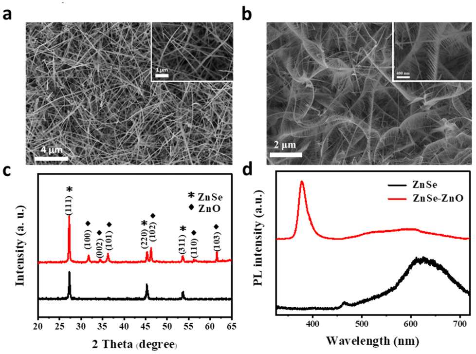 | ||
| Fig. 1 (a and b) SEM images of ZnSe NWs and comb-like ZnO–ZnSe NW heterostructures, respectively. (c) XRD patterns and (d) PL spectra of ZnSe NWs and ZnO–ZnSe NW heterostructures, respectively. | ||
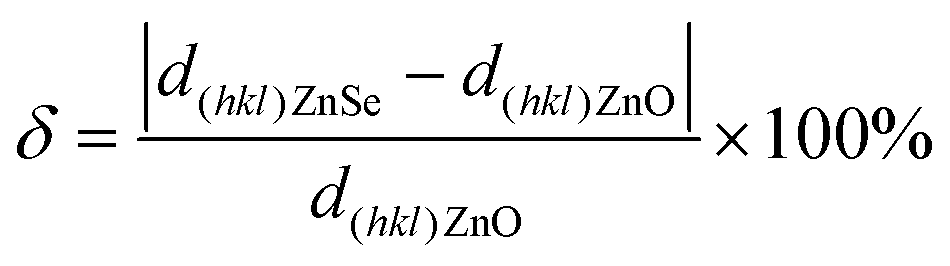
TEM was performed to further investigate the crystallographic structure and examine the growth mechanism of the ZnO–ZnSe NWs. Fig. 2a shows a low-magnification TEM image of the comb-like branched ZnO–ZnSe heterostructure. EDS line profiles of the NWs were recorded to investigate the distribution of the constituent elements in the ZnO–ZnSe hetero-structured NWs. The EDS line-scan images in Fig. S3† indicate the distributions of three elements: Se, Zn, and O. The prominent peaks of the Se K-edge signal clearly define the ZnSe backbone region, which is marked by a blue rectangle in Fig. S2(b–d).† The red spectrum, corresponding to the Zn K-edge signal, was observed throughout the heterostructure, as shown in Fig. S3c.† By comparison, the green oxygen K-edge signal shows a similar dispersion but with much weak intensity on the ZnSe backbone side (Fig. S3d†), which further verifies the asymmetric growth of the ZnO NWs. It was found that cone-shaped ZnO NWs with non-uniform diameters were selectively grown on one side of the ZnSe NWs. Due to the relatively rapid preferred orientation growth of ZnO in the axial direction, a delayed radial expansion occurred, leading to the formation of cone-shaped ZnO nanowires. In addition, three typical areas in the branched heterostructures (topside ZnO, the ZnO–ZnSe interface, and ZnSe NWs) were selected for investigation and their corresponding high-resolution TEM (HRTEM) images are shown in Fig. 2(b–d). First, the diffraction spots in the FFT images of the selected locations (insets of Fig. 2(b and c)) confirm the highly crystalline nature of the ZnO branches and ZnSe backbone. Second, the HRTEM image shows clear lattice spacings of 0.246 and 0.328 nm, in agreement with the (101) plane of ZnO (wurtzite structure) and the (111) lattice plane of ZnSe (zinc blende structure), respectively. Moreover, a relatively small lattice mismatch plays an important role in the growth of highly crystalline structures at heterogeneous interfaces.24,25 According to Turnbull and Vonnegut's research,24 heterogeneous nucleation tends to occur coherently when lattice mismatch is less than 5%. The one-dimensional lattice mismatch was calculated using the following equation:
 | (1) |
![[1 with combining macron]](https://www.rsc.org/images/entities/char_0031_0304.gif) 20) planes of ZnO are parallel to the (
20) planes of ZnO are parallel to the (![[2 with combining macron]](https://www.rsc.org/images/entities/char_0032_0304.gif) 20) planes of ZnSe, and both extend in the same direction as ZnO NW growth. The small lattice mismatch between the {102} planes of ZnO (d-pacing = 1.911 Å) and the {220} planes of ZnSe (d-spacing = 1.968 Å) is 2.98%, which contributes to the growth of highly crystallized heterostructures. The reverse sides of the highly crystallized ZnSe NWs are covered by polycrystalline ZnO shells (Fig. S4†), which indicates the asymmetric growth of ZnO on the two opposite surfaces. The selective growth of ZnO may be attributed to the surface polarity of the ZnSe backbones.26–28 Depending on the electronegativity (EN) of both elements, the Zn (EN = 1.65) side is positively polarized, whereas the Se (EN = 2.55) side is negatively polarized. Therefore, the binding energy between [Zn(g)] (gasifying Zn atoms) and [Se(s)] (negatively polar surfaces) is larger than that between [Zn(g)] and [Zn(s)] (positively polar surfaces). In addition, the Zn vacancies in the ZnX NWs contribute to the non-uniform growth of nanostructures on the inactive sites (positive polar surfaces).29 These are the reasons for the asymmetric growth of ZnO NWs on the surface of the ZnSe NWs.
20) planes of ZnSe, and both extend in the same direction as ZnO NW growth. The small lattice mismatch between the {102} planes of ZnO (d-pacing = 1.911 Å) and the {220} planes of ZnSe (d-spacing = 1.968 Å) is 2.98%, which contributes to the growth of highly crystallized heterostructures. The reverse sides of the highly crystallized ZnSe NWs are covered by polycrystalline ZnO shells (Fig. S4†), which indicates the asymmetric growth of ZnO on the two opposite surfaces. The selective growth of ZnO may be attributed to the surface polarity of the ZnSe backbones.26–28 Depending on the electronegativity (EN) of both elements, the Zn (EN = 1.65) side is positively polarized, whereas the Se (EN = 2.55) side is negatively polarized. Therefore, the binding energy between [Zn(g)] (gasifying Zn atoms) and [Se(s)] (negatively polar surfaces) is larger than that between [Zn(g)] and [Zn(s)] (positively polar surfaces). In addition, the Zn vacancies in the ZnX NWs contribute to the non-uniform growth of nanostructures on the inactive sites (positive polar surfaces).29 These are the reasons for the asymmetric growth of ZnO NWs on the surface of the ZnSe NWs.
 | ||
| Fig. 2 (a) Low-magnification TEM image of comb-like ZnO–ZnSe heterostructures. The HRTEM images of (b) ZnO nanowires and (c) the interface between ZnSe nanowires and ZnO nanowires. The inset shows the corresponding FFT pattern from the dashed line square for ZnO (orange) and ZnSe (red). (d) Atomic-scale image from the white square-framed region in (c). Marked spacings of 0.246 and 0.328 nm in the HRTEM image correspond to the (101) plane of ZnO and the (111) plane of ZnSe, respectively. | ||
To obtain ZnO–ZnSe heterostructures with different lengths of ZnO NWs, different parameters are presented below. The influence of three primary controllable parameters, namely temperature, vacuum pressure, and reaction time, is discussed in the follow parts.
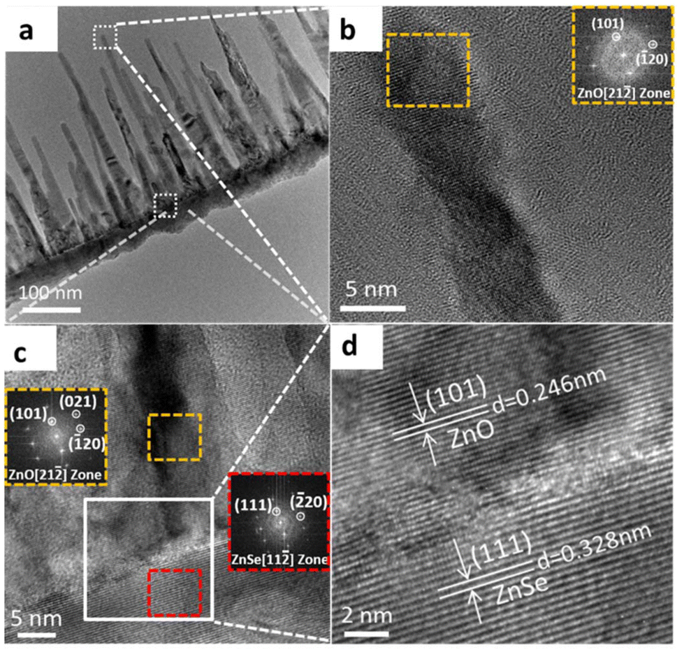
First, for the effect of temperature, 325 mesh-Zn powder with a bulk-type melting point of 419.53 °C and a boiling point of 907 °C was used as the raw material for the synthesis of ZnO NWs. A powder with high surface energy under vacuum conditions should have a much lower boiling point than that of its bulk-type nature. Fig. S5(a–f)† display the SEM and PL results of samples grown at 600 °C, 550 °C, and 500 °C. The results suggest that hetero-structured ZnO NWs cannot be formed at an annealing temperature of Ta > 550 °C. This phenomenon may be due to the elevated kinetic energy of the Zn vapor and the increased surface free energy of the ZnSe NWs at elevated temperatures, rendering them less conducive to the nucleation and axial crystal growth of ZnO. In this study, 500 °C was chosen for the growth of ZnO NWs on the surface of the ZnSe NWs. The length of the ZnO NWs could be controlled at 500 °C by changing the vacuum pressure and reaction time. Fig. 3(a–d) display the representative morphologies at different growth pressures (1, 5, 20, and 40 torr). It was found that ZnO NWs were not formed at 1 torr. The growth of ZnO NWs exhibits a linear relationship with the operating pressure. Also, as shown in Fig. 3(e–h), the length of the ZnO NWs increases upon extending the reaction time. These results indicate that ZnO–ZnSe heterostructures with ZnO NWs of different lengths can be modulated by varying the reaction temperature, vacuum pressure, and reaction time.
 | ||
| Fig. 3 Controllable growth of comb-like ZnO–ZnSe heterostructures. (a–d) Different growth pressures at a temperature of 500 °C with a growth time of 30 min (e–h) Different growth times at a temperature of 500 °C and a pressure of 20 torr. Scale bar: 600 nm. | ||
To assess the photodetection performance of the as-prepared NWs, Ag NWs as transparent electrodes (TEs) and ZnO–ZnSe NWs were integrated onto a transparent polyimide (PI) substrate (device fabrication and measurements). Fig. S6† illustrates a schematic of the fabrication process of the all-NW photodetector with the Ag NW electrode. First, we used the contact printing method to transfer the as-grown ZnO–ZnSe hetero-structured NWs from Si substrates to PI/PDMS substrates. The metal hard mask was then covered with PI. Finally, Ag NW electrodes were fabricated using the orthogonal blade coating method (Fig. S7†) to form finger-shaped transparent conducting electrodes with a channel length of 0.4 mm and a channel width of 0.045 mm. The effective working area between the finger electrodes was estimated to be 0.18 mm2. A Keithley 4200 semiconductor characterization system (SCS) was used to evaluate the photoresponse of the device under three different light sources: blue (405 nm), green (532 nm), and red (633 nm). All the results presented below were measured under 1.4 mW mm−2 light illumination at room temperature. The lengths of the ZnO NWs were controlled by varying the growth time. Because the electronic properties of 1D ZnO NWs are length-dependent,30 it is important to investigate their length-dependent optoelectronic properties. As shown in Fig. 4(a, c, e, and g), three different lengths of ZnO NWs were investigated: short (∼300 nm), medium (∼600 nm), and long (∼1000 nm) lengths of ZnO NWs, which are denoted as ZnO(s)–ZnSe, ZnO(m)–ZnSe, and ZnO(l)–ZnSe, respectively. As shown in Fig. S8,† the I–V curves of all devices showed an ultralow dark current (∼1 pA). Numerous junction sites with high junction barriers increase the total inner resistance of the NW network. Therefore, an extremely low dark current can be achieved.31–33 Current vs. time (I–T) data for the as-prepared samples were obtained by periodically blocking the light sources at an applied voltage of 10 V. As shown in Fig. 4(b, d, f, and h), when pure ZnSe NWs were illuminated by a 405 nm blue light, the photocurrent, defined as Iph = Ilight − Idark, significantly increased to 492.9 pA in comparison with the dark current (0.142 pA). This result suggests that an acceptable photocurrent-to-dark current ratio (on/off ratio: Iph/Idark) of 3464 can be obtained, which is higher than those obtained in previous studies.34 However, pure ZnSe exhibited a low photocurrent with only 8.846 and 3.526 on–off ratios under green and red-light illumination, respectively. These results indicate that pure ZnSe NWs have a higher photoresponse. However, the ZnO–ZnSe heterostructure showed an increased response and decay time with increasing length of ZnO NWs under 405 nm blue light illumination at 10 V. For the response to green light (532 nm), the heterojunctions showed a much higher responsivity than pure ZnSe NWs and displayed a volcano-shaped response. Among them, the ZnO–ZnSe heterojunctions showed the highest response (45 pA) under green light illumination, which is much higher than that of pure ZnSe NWs (∼1 pA). The dark currents of all samples are almost the same and the on–off ratios increase from 8.85 to 210.97 (green) and 3.53 to 28.5 (red). Furthermore, the photon energies corresponding to red (1.96 eV) and green (2.33 eV) light are lower than those of ZnO (3.37 eV) and ZnSe (2.67 eV) and are incapable of promoting direct band photoexcitation on either side. The improved photoresponse can be attributed to the following factors. First, the enhanced photon absorption at the ZnO–ZnSe interface is an indirect type-II transition absorption. The schematic of the thermal equilibrium band diagram is shown in Fig. S9.† The heterojunctions could respond to red and green light, which may be due to the intermediate transition of band levels, in which the electrons transformed from the valence band of ZnSe to the conduction band of ZnO.35 Second, additional ZnO nanostructures also reduce the contact barrier between ZnSe and Ag NWs by forming ohmic contacts. In addition, the intimate contact between ZnO and ZnSe, which was confirmed by HRTEM, was conducive to the fast transfer of photogenerated carriers. Third, 1D branched structures with large surface-to-volume ratios can adsorb more oxygen molecules on the surface and capture the free electrons present in the n-type ZnO NWs. This results in a thicker charge depletion layer, thereby reducing the dark current as follows:
| O2 + e− → O2−(adsorbed) |
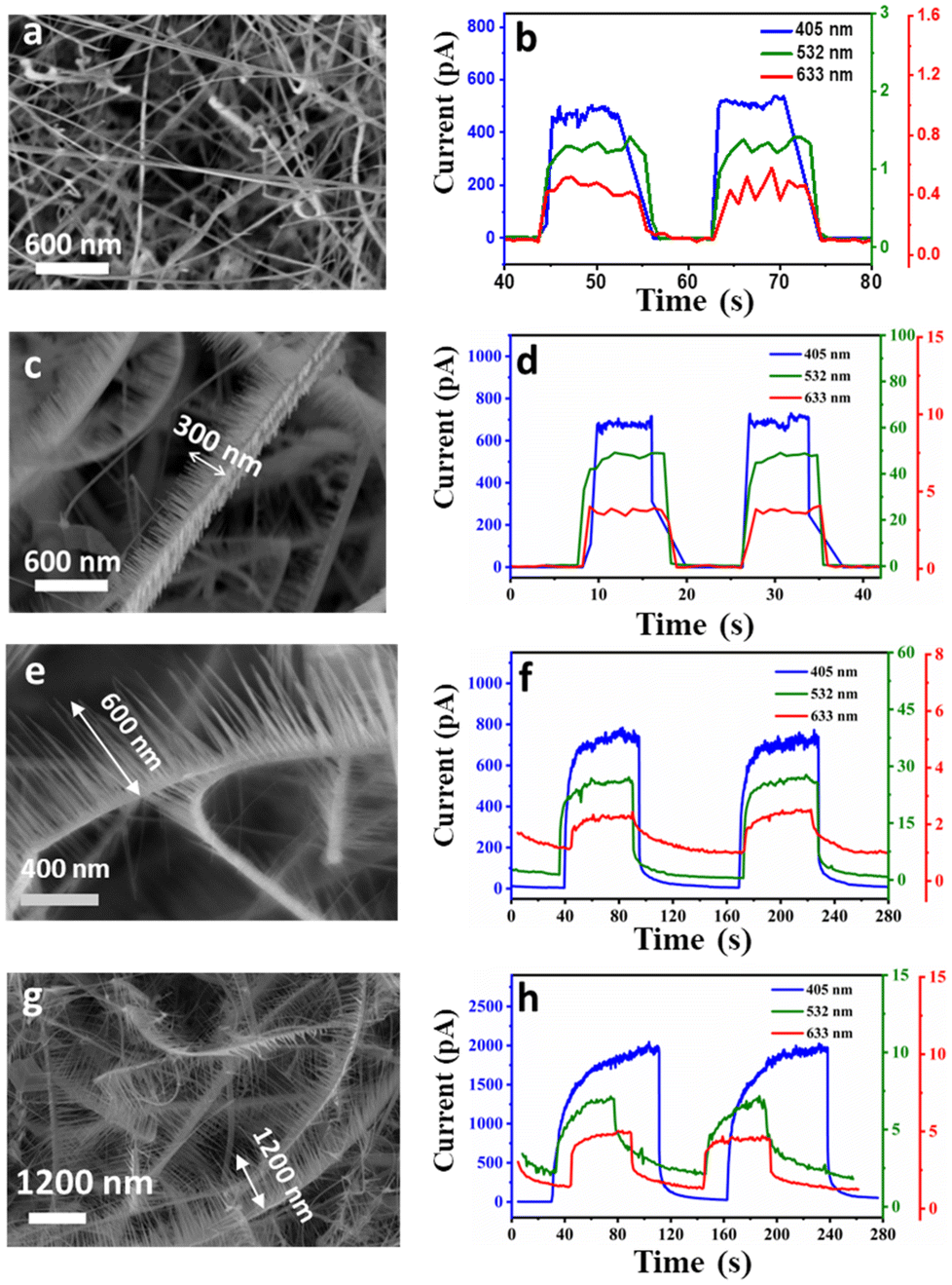 | ||
| Fig. 4 SEM image of comb-like ZnO–ZnSe heterostructures with different lengths of ZnO NWs: (a) pristine ZnSe; (c) ZnO(s)–ZnSe, (e) ZnO(m)–ZnSe, and (g) ZnO(l)–ZnSe. The corresponding I–t curves of (b) pristine ZnSe, (d) ZnO(s)–ZnSe, (f) ZnO(m)–ZnSe, and (h) ZnO(l)–ZnSe under 405, 532, and 633 nm light illumination at 10 V bias. | ||
When the device is illuminated with light, electron–hole pairs are generated in ZnO, and the adsorbed oxygen ions instantaneously combine with the holes and release free electrons via the reaction as follows:
| O2−(adsorbed) + h+ → O2(g) |
This reaction leads to a reduction in the depletion barrier thickness and an increased photocurrent. The electron–hole pairs excited by indirect bandgap absorption also ameliorated this mechanism. Finally, the multiple light scattering enhanced by the ZnO branches can further increase light absorption, which benefits the photoresponse. Finally, the indirect recombination and surface recombination of excited charges can be reduced by heat treatment under a Zn-rich atmosphere.36,37 Therefore, an appropriate length of ZnO NWs loaded on the ZnSe NWs increased the photoresponse of the device and extended the photoresponse band. Considering ZnO(s)–ZnSe as an example, it shows a higher photoresponse to the three types of light illumination (Fig. 5(a–c)). In particular, for the green and blue light, increases of 3835% and 798% in photocurrent were observed in the green and red-light spectra of the ZnO(s)–ZnSe NW heterostructure, respectively. As mentioned earlier, the most apparent difference in the photoresponse between ZnSe and ZnO NWs was the response time. The time taken for the current to increase from 10% to 90% of the peak value, and vice versa, is defined as the rise and decay times, respectively. To compare the response times of the different devices, the photocurrent was fitted using a first-order exponential equation:
| ΔIphoto(t) = Idark + Ae(t/τ) |
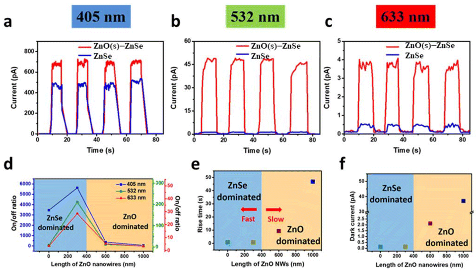 | ||
| Fig. 5 I–t curves of pure ZnSe NWs and ZnO–ZnSe(s) NWs at (a) 405 nm, (b) 532 nm, and (c) 633 nm light illumination. Illustration of ZnSe or ZnO dominated optoelectronic characteristics at different lengths of ZnO NWs. The terms include (d) on/off ratio, (e) rise time, and (f) dark current. | ||
To examine the flexibility of the all-nanowire devices, ZnO(s)–ZnSe NWs were selected for bending under 405 nm irradiation. Optical photographs of different radii of curvature are shown in Fig. 6a. The changes in the photocurrent with and without bending are defined by the photocurrent ratio (I/I0). As shown in Fig. 6b, the ratios displayed negligible changes under severe bending with a radius of curvature below 5 mm. In addition, a slight decrease of 4% in the photocurrent was observed under a 2 mm radius of curvature. These results confirm the excellent flexibility of the all-NW device. Fig. 6c illustrates the normalized I–t curves for the stable dark-current and photocurrent devices under bending with different radii of curvature. To investigate the durability limit, the performance of the all-nanowire device was analyzed during dynamic bending tests for 1000 cycles at a radius of curvature of 2 mm, as shown in Fig. 6d and e. Notably, the photocurrent begins to decrease at a radius of curvature of 2 mm. In the bending test, no degradation was observed when the radius of curvature was greater than 5 mm. With increasing cycles from 0 to 1000 under tensional bending, the photocurrent decreased to only approximately 45% at 500 bending cycles compared to its pristine state and showed no further decrease until 1000 bending cycles. The results of the bending test suggest excellent durability of the all-NW devices prepared by the low-cost printing method.
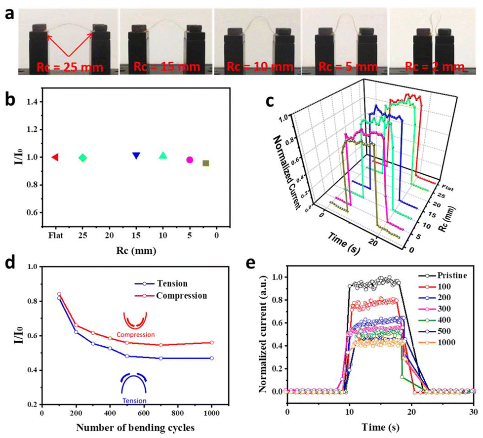 | ||
| Fig. 6 Photographs of devices with different bending radii (Rc). (b) Photocurrent ratios before and after bending. I0 is the photocurrent before bending and I is the photocurrent after bending. (c) Normalized current as a function of real time with different Rc values. (d) Change of the photocurrent ratio after 1000 bending cycles under compressive and tensile strains, respectively. (e) I–t plots for different bending times under tensile strain. The harsh bending radius for (d) and (e) is 2 mm. | ||
In summary, we report the controlled synthesis of 1D–1D comb-like ZnO–ZnSe heterostructure NWs with different lengths of ZnO via a well-designed two-step process. The ZnO NWs are anchored on the sides of the ZnSe NWs to form a comb-like 1D–1D ZnO–ZnSe heterostructure. The heterostructure is integrated with Ag NWs to construct a flexible photodetector using a low-cost printing method. The device exhibits an extended photodetection region owing to the formation of an intermediate band between ZnO and ZnSe. In particular, the ZnSe NWs with an appropriate length of ZnO branches showed increased photoresponses of 3835% and 798% than that of pure ZnSe NWs under green and red-light irradiation, respectively. In addition, the device exhibits superior folding endurance after 1000 bending tests. This study provides useful insights for the design and fabrication of novel heterostructure materials for high-performance photodetectors.
Conflicts of interest
There are no conflicts to declare.Acknowledgements
This research was supported by the National Science and Technology Council through grant numbers 110-2622-E-007-017, 110-2634-F-007-023-, 110-2112-M-007-032-MY3, 111-2218-E-007-015-MBK, 112-2628-E-007-019, and 113-2119-M-007-015-MBK and the National Synchrotron Radiation Research Center (NSRRC). The authors acknowledge using HRTEM and ESCA equipment from the Instrument Center of National Tsing Hua University.References
- X. Li, X. Liu, Y. Li, D. Gao and L. Cao, IEEE Access, 2021, 9, 11954–11973 Search PubMed.
- X. Fang, Y. Bando, M. Liao, T. Zhai, U. K. Gautam, L. Li, Y. Koide and D. Golberg, Adv. Funct. Mater., 2010, 20, 500–508 CrossRef CAS.
- X. Fang, S. Xiong, T. Zhai, Y. Bando, M. Liao, U. K. Gautam, Y. Koide, X. Zhang, Y. Qian and D. Golberg, Adv. Mater., 2009, 21, 5016–5021 CrossRef CAS PubMed.
- X. Liu, L. Gu, Q. Zhang, J. Wu, Y. Long and Z. Fan, Nat. Commun., 2014, 5, 4007 CrossRef CAS PubMed.
- C. H. Hsiao, S. J. Chang, S. B. Wang, S. P. Chang, T. C. Li, W. J. Lin, C. H. Ko, T. M. Kuan and B. R. Huang, J. Electrochem. Soc., 2009, 156, J73–J76 CrossRef CAS.
- L. Peng, L. Hu and X. Fang, Adv. Mater., 2013, 25, 5321–5328 CrossRef CAS PubMed.
- Z. Zhang, Z. Kang, Q. Liao, X. Zhang and Y. Zhang, Chin. Phys. B, 2017, 26, 118102 CrossRef.
- C. L. Hsu and S. J. Chang, Small, 2014, 10, 4562–4585 CrossRef CAS PubMed.
- Q. Su, L. Li, S. Li and H. Zhao, Mater. Lett., 2013, 92, 338–341 CrossRef CAS.
- P. Rong, Y.-F. Jiang, Q. Wang, M. Gu, X.-L. Jiang and Q. Yu, J. Mater. Chem. A, 2022, 10, 6231–6241 RSC.
- Q. Yu, T. Ai, L. Jiang, Y. Zhang, C. Li and X. Yuan, RSC Adv., 2014, 4, 53946–53949 RSC.
- Q. Shi, Z. Luo, L. Jiang, X. Li, C. Bai and Q. Yu, Mater. Lett., 2023, 350, 134952 CrossRef CAS.
- Z. Mu, Q. Zheng, R. Liu, M. W. I. Malik, D. Tang, W. Zhou and Q. Wan, Adv. Electron. Mater., 2019, 5, 1800770 CrossRef.
- S. Chang, C. Hsiao, B. Lan, S. Hung, B. Huang, S. Young, Y. Cheng and S. Chih, Superlattices Microstruct., 2010, 48, 50–57 CrossRef CAS.
- Z. Lou, L. Li and G. Shen, Nanoscale, 2016, 8, 5219–5225 RSC.
- S.-J. Chang, C. Hsiao, S.-C. Hung, S. Chih, B. Lan, S. Wang, S.-P. Chang, Y. Cheng, T. Li and B.-R. Huang, J. Electrochem. Soc., 2009, 157, K1 CrossRef.
- Y. Ning, Z. Zhang, F. Teng and X. Fang, Small, 2018, 14, 1703754 CrossRef PubMed.
- L. Hu, J. Yan, M. Liao, H. Xiang, X. Gong, L. Zhang and X. Fang, Adv. Mater., 2012, 24, 2305–2309 CrossRef CAS PubMed.
- W. Tian, C. Zhang, T. Zhai, S. L. Li, X. Wang, J. Liu, X. Jie, D. Liu, M. Liao and Y. Koide, Adv. Mater., 2014, 26, 3088–3093 CrossRef CAS PubMed.
- J. Tersoff, Nano Lett., 2015, 15, 6609–6613 CrossRef CAS PubMed.
- H. K. Yu and J.-L. Lee, Sci. Rep., 2014, 4, 1–8 Search PubMed.
- U. Philipose, T. Xu, S. Yang, P. Sun, H. E. Ruda, Y. Q. Wang and K. L. Kavanagh, J. Appl. Phys., 2006, 100, 084316 CrossRef.
- U. Philipose, S. Ankur, E. R. Harry, P. J. Simpson, Y. Q. Wang and K. L. Kavanagh, Nanotechnology, 2008, 19, 215715 CrossRef CAS PubMed.
- D. Turnbull and B. Vonnegut, Ind. Eng. Chem., 1952, 44, 1292–1298 CrossRef CAS.
- L. Wang, L. Yang, D. Zhang, M. Xia, Y. Wang and J. G. Li, Metall. Mater. Trans. A, 2016, 47, 5012–5022 CrossRef CAS.
- Z. L. Wang, X. Y. Kong and J. M. Zuo, Phys. Rev. Lett., 2003, 91, 185502 CrossRef CAS PubMed.
- M. de la Mata, R. R. Zamani, S. Martí-Sánchez, M. Eickhoff, Q. Xiong, A. Fontcuberta i Morral, P. Caroff and J. Arbiol, Nano Lett., 2019, 19, 3396–3408 CrossRef CAS PubMed.
- S. Acharya, A. B. Panda, S. Efrima and Y. Golan, Adv. Mater., 2007, 19, 1105–1108 CrossRef CAS.
- Y.-Z. Long, M. Yu, B. Sun, C.-Z. Gu and Z. Fan, Chem. Soc. Rev., 2012, 41, 4560–4580 RSC.
- I. Musa, N. Qamhieh and S. T. Mahmoud, Results Phys., 2017, 7, 3552–3556 CrossRef.
- J. Wang, C. Yan, M.-F. Lin, K. Tsukagoshi and P. S. Lee, J. Mater. Chem. C, 2015, 3, 596–600 RSC.
- Y. Pei, R. Pei, X. Liang, Y. Wang, L. Liu, H. Chen and J. Liang, Sci. Rep., 2016, 6, 21551 CrossRef CAS PubMed.
- H. Zhang, Z. Wang, J. Chen, C. Tan, S. Yin, H. Zhang, S. Wang, Q. Qin and L. Li, Nanoscale, 2022, 14, 16130–16138 RSC.
- E. Oksenberg, R. Popovitz-Biro, K. Rechav and E. Joselevich, Adv. Mater., 2015, 27, 3999–4005 CrossRef CAS PubMed.
- S. Yan, S. C. Rai, Z. Zheng, F. Alqarni, M. Bhatt, M. A. Retana and W. Zhou, Adv. Electron. Mater., 2016, 2, 1600242 CrossRef.
- U. Philipose, T. Xu, S. Yang, P. Sun, H. E. Ruda, Y. Wang and K. Kavanagh, J. Appl. Phys., 2006, 100, 084316 CrossRef.
- K. Tang, M. Jiang, B. Yang, T. Xu, Z. Liu, P. Wan, C. Kan and D. Shi, Nanoscale, 2023, 15, 2292–2304 RSC.
- C.-C. Huang, H. Medina, Y.-Z. Chen, T.-Y. Su, J.-G. Li, C.-W. Chen, Y.-T. Yen, Z. M. Wang and Y.-L. Chueh, Nano Lett., 2016, 16, 2463–2470 CrossRef CAS PubMed.
- M. Peng, Z. Wen and X. Sun, Adv. Funct. Mater., 2023, 33, 2211548 CrossRef CAS.
- D. Wu, Y. Xu, H. Zhou, X. Feng, J. Zhang, X. Pan, Z. Gao, R. Wang, G. Ma and L. Tao, InfoMat, 2022, 4, e12320 CrossRef CAS.
- C. Soci, A. Zhang, B. Xiang, S. A. Dayeh, D. P. R. Aplin, J. Park, X. Y. Bao, Y. H. Lo and D. Wang, Nano Lett., 2007, 7, 1003–1009 CrossRef CAS PubMed.
Footnotes |
| † Electronic supplementary information (ESI) available. See DOI: https://doi.org/10.1039/d3nr06617g |
| ‡ These authors contributed equally to this work. |
| This journal is © The Royal Society of Chemistry 2024 |