
 Open Access Article
 This Open Access Article is licensed under a Creative Commons Attribution-Non Commercial 3.0 Unported Licence
Study of a charge transition-driven resistive switching mechanism in TiO2-based random access memory via density functional theory†
Taeyoung
Jeong
 ab,
In Won
Yeu
a,
Kun Hee
Ye
ab,
Seungjae
Yoon
ab,
Dohyun
Kim
ab,
Cheol Seong
Hwang
*b and
Jung-Hae
Choi
*a
ab,
In Won
Yeu
a,
Kun Hee
Ye
ab,
Seungjae
Yoon
ab,
Dohyun
Kim
ab,
Cheol Seong
Hwang
*b and
Jung-Hae
Choi
*a
aElectronic Materials Research Center, Korea Institute of Science and Technology, Seoul 02792, Korea. E-mail: choijh@kist.re.kr
bDepartment of Materials Science and Engineering and Inter-University Semiconductor Research Center, Seoul National University, Seoul 08826, Korea. E-mail: cheolsh@snu.ac.kr
First published on 29th February 2024
Abstract
The nature of the conducting filament (CF) with a high concentration of oxygen vacancies (VOs) in oxide thin film-based resistive random access memory (RRAM) remains unclear. The VOs in the CF have been assumed to be positively charged (VO2+) to explain the field-driven switching of RRAM, but VO2+ clusters in high concentration encounter Coulomb repulsion, rendering the CF unstable. Therefore, this study examined the oxidation state of VOs in the CF and their effects on the switching behavior via density functional theory calculations using a Pt/TiO2/Ti model system. It was concluded that the VOs in the CF are in a low oxidation state but are transformed to VO2+ immediately after release from the CF. In addition, the short-range interactions between VOs were confirmed to facilitate the rupture and rejuvenation of the CF by reducing the required activation energy. Finally, an improved switching model was proposed by considering the charge transition of VOs, providing a plausible explanation for the reported coexistence of two opposite bipolar switching polarities: the eight-wise and the counter-eight-wise polarities.
1. Introduction
Metal–oxide-based resistive random-access memory (RRAM) is a promising next-generation memory device due to its low power consumption, high performance, and compatibility with current complementary metal oxide semiconductor technology. RRAM is currently applied to state-of-the-art applications such as process-in-memory and neuromorphic computing.1–3 However, its operation mechanism is not fully understood yet, hampering systematic research on RRAM.For valence-change type memory (VCM), the redistribution of oxygen vacancies (VOs) in the conducting filament (CF) in response to applied bias is widely accepted as the major source of resistive switching.4,5 However, there is still controversy about the charge state of VOs in the CF. Based on their field-driven characteristic, it has been argued that the VOs should be positively charged (that is, VO2+). On the other hand, other recent studies questioned the VO2+ argument because the CF with a high VO2+ concentration would be unstable due to the Coulomb repulsion.6–8 Lee et al. suggested that the CF consists of VO0s rather than VO2+s.7 They experimentally observed the acceleration of CF destruction once devices are illuminated by a green-light laser, enhancing a charge transition from VO0 to VO2+. They argued that this finding indicates that the original CF was composed of VO0s. They also confirmed that the CF composed of VO0s is more stable than the one composed of VO2+s through density functional theory (DFT) calculations. Furthermore, Park et al. proposed a modified physical model that incorporated the charge transition from VO2+ to VO0 when the concentration of VO exceeds a threshold value.8 The model allowed them to explain secondary set and retention failure, which the conventional model could not explain. Nevertheless, a theoretical study dealing with the evolution in oxidation number (ON) of VO during the switching process is required to elucidate the effects of the charge transition of VOs on the switching behavior.
Meanwhile, in bipolar-type resistive switching (BRS) devices, two opposing switching polarities were reported: the counter-eight-wise (c8w) and the eight-wise (8w) polarities. The c8w polarity is more general and corresponds to the case where the set and reset occur by applying negative and positive voltages to the active electrode, respectively.9 The active electrode refers to the electrode where switching occurs in the nearby switching film and is usually identified as the electrode with a higher work function. For VCM devices, the c8w BRS mode is well understood via a field-driven drift of VO2+s. In contrast, the 8w BRS mode, an abnormal case where the set and reset occur by positive and negative voltages applied to the active electrode, respectively, has occasionally been observed in various oxides such as TiO2, HfO2, and SrTiO3.10–16 However, its origin is still under debate. Furthermore, both BRS modes can simultaneously appear in several VCM devices, as shown in Fig. 1, where the red and green lines represent the c8w and 8w BRS modes. This unusual I–V curve has been reported in TiO2, Ta2O5, and Al2O3-based devices.10–12,17,18 For TiO2 systems, there is no common consensus for the origin of the 8w BRS mode. For Pt/TiO2/Ti devices, Yin et al. attributed this abnormal BRS mode to the electron trapping/detrapping effects at the interfacial states.10 Zhang et al., on the other hand, argued that the 8w BRS mode arises from the exchange of oxygen ions between the Pt electrode and TiO2 layer at the Pt/TiO2 interface.11 For Pt/TiO2/Pt devices, Miao et al. suggested that the switching polarity is determined by which electrode, top or bottom, dominantly participates in the switching process,12 while Kim et al. explained that the switching mode depends on the shape of the CF.13 Accordingly, the mechanism of the 8w BRS mode in TiO2-based devices remains controversial, especially when two opposite BRS modes coexist.
 | ||
| Fig. 1 Characteristic I–V curve exhibiting the coexistence of the c8w polarity (red) and the 8w polarity (green). LRS and HRS represent the low resistance state and high resistance state, respectively. The asterisks indicate that they are involved in the 8w polarity. | ||
Therefore, this work shows the comprehensive DFT calculation results for a Pt/TiO2/Ti model system with two main objectives: (1) elucidating the evolution in ON of VO during switching and (2) proposing an improved mechanism encompassing both the c8w and 8w BRS modes. The Pt electrode was chosen as the active electrode due to its high work function. In this paper, the voltage is assumed to be applied to the Pt electrode while the Ti electrode is grounded. The 8w BRS mode of the Pt/TiO2/Ti device was assumed to be filamentary type, based on the observation that the resistance value of the low resistance state (LRS) of the 8w BRS mode does not show area-dependency.11 The Results and discussion of this paper are organized as follows: section A investigates the interaction between VOs considering their ON; section B examines a suitable CF structure and its preference for the oxidation state; finally, section C provides a comprehensive explanation of the charge transition of the VO and suggests a plausible origin for the coexistence of the two BRS modes in Pt/TiO2/Ti devices.
2. Computational methods
The Vienna ab initio simulation package (VASP) was adopted for all DFT calculations using local density approximation (LDA) parameterized by Ceperley and Alder for the exchange–correlation functional.19–22 The plane wave cutoff energy of 500 eV and Monkhorst–Pack 4 × 4 × 6 k-points were used for the conventional rutile unit cell of TiO2. The k-points for supercells were scaled to keep the same k-point density as the unit cell. The atomic structures were relaxed until the Hellmann–Feynman forces were below 0.02 eV Å−1. The 3s, 3p, 3d, and 4s orbitals of Ti and the 2s and 2p orbitals of O were treated as valence electrons. In order to mitigate a well-known bandgap underestimation of the conventional LDA calculations, the LDA+U approach suggested by Dudarev et al. was implemented to correct the on-site Coulomb interactions, with the U parameter for Ti 3d orbitals, Ud, of 4.0 eV and that for O 2p orbitals, Up, of 9.0 eV.23 The J parameter for Hund's coupling was fixed at 0 eV. All calculations included the spin polarization effects. The calculated lattice parameters of rutile TiO2 were (a, b, c) = (4.543 Å, 4.543 Å, 2.957 Å), indicating good agreement with the experimental values within 1%.24 The calculated bandgap of 2.51 eV, closer to the experimental bandgap of 3.0 eV than that obtained by the conventional LDA calculations of 1.81 eV, did not completely mitigate the bandgap underestimation problem.25 However, the calculated defect states and formation energies of a VOq+ (q = 0, 1, 2) showed feasible agreements with previous Heyd–Scuseria–Ernzerhof (HSE) or DFT+GW studies, as described in Fig. S1,† demonstrating the reliability of our calculation conditions.26,27To simulate the various arrangements of VOs, such as in the CF, they were introduced into the 3 × 3 × 6 supercells of rutile TiO2 while keeping the lattice parameters fixed. This supercell was confirmed to sufficiently prevent unintended interactions between image cells, even if there are multiple VOs inside. The formation energy (Ef) of a charged VO was calculated as follows:
| Ef(VOq+) = Etot(VOq+) − Etot(TiO2) + μO + q(VBM + PA + εf), | (1) |
To clarify the discussion, the ON was classified into average oxidation number (AON) and individual oxidation number (ION). AON represents the average ON of all VOs within a supercell and is determined by dividing the total charge by the number of VOs in the supercell. In this study, the AON was considered for all instances in which the number of electrons in the supercell is an integer. For example, for a supercell containing two VOs, four electrons can be removed since each VO can accommodate up to two electrons. Accordingly, five AONs (0, +0.5, +1, +1.5, +2) can be considered. Meanwhile, in a supercell where VO sites are not symmetrically equivalent, individual VOs may have distinct ONs that are different from the AON. This specific ON for each VO is termed ION. To the authors’ knowledge, the ION of VO has not been estimated, presumably due to the difficulties in its direct calculation. The conventional ON calculation methodologies, such as Bader charge (BC) analysis, apply only to ions but not to vacancies. Accordingly, this study devised an alternative approach to estimate the ION. It was revealed that, in rutile TiO2, the sum of BC values of three neighboring Ti ions (∑BC) surrounding a certain VO is determined by the ION of the VO and the coordination numbers (CNs) of these three Ti ions. Other nearby VOs hardly affect the ∑BC value, as shown in Fig. S2.† Consequently, the ION of each VO can be estimated via the ∑BC value and CN distribution of neighboring Ti ions. The full description of this approach is provided in the ESI and Fig. S2–S6.† The sum of IONs obtained from the approach was compared with the actual total charge of the supercell to validate this proposed approach. These two values are sufficiently identical within an error of less than 3%, as shown in Table S1.†
For both the BC analysis and the activation energy (Ea) calculations, open-source codes were implemented.28–30 A default setting was used for the BC analysis. For the Ea calculations, on the other hand, the climbing nudged elastic band (cNEB) method was used, and the images were stabilized until the forces were less than 0.05 eV Å−1.
3. Results and discussion
A. Interaction between VOs
The long-range interaction between two charged vacancies can be understood through the Coulomb interaction. Besides, other factors, such as lattice distortion caused by vacancies, may also play a role in the short-range interaction, which is non-negligible in CFs with a high concentration of VOs. For comprehending the short-range interaction, the cohesive energy (Ecoh) was calculated as follows:| Ecoh(VOq+) = Ef(two VOq+, d) − 2Ef(VOq+) | (2) |
The first term on the right-hand side is the Ef of two VOq+s separated by a distance of d, while the second term is that of an isolated VOq+ multiplied by a factor of 2. Fig. 2a shows the calculated results, where five AONs from 0 to +2 with increments of +0.5 were considered. For supercells containing two VOs, their sites are symmetrically equivalent irrespective of d since all O sites in rutile are symmetrically equivalent. Accordingly, the two VOs must exhibit an identical ION (i.e., q+ = ION = AON).
 | ||
| Fig. 2 (a) Ecoh as a function of the distance between two VOq+s (q = 0, 0.5, 1, 1.5, and 2) in rutile TiO2. (b) Atomic structure of rutile TiO2 viewing along the [110] direction (left panel) and size of the Ti–O octahedron constituting the rutile TiO2 (right panel). The bold rectangle (and line) and dotted line represent the equatorial plane and the vertical axis of the Ti–O octahedron, respectively. The numerical values adjacent to the blue lines indicate the distances between two oxygen ions in units of Å. Grey, red, and yellow circles indicate Ti, O, and VO, respectively. This color notation is maintained throughout this paper. Electron clouds for (c) an isolated VO0, (d) two VO0s separated by a distance of 3.88 Å, and (e) two VO0s separated by a distance of 4.42 Å, respectively (isosurface = 0.005 e Å−1). The two electron clouds in (e) are located in two immediately adjacent (110) planes. | ||
For VO2+, the overall trend of the Ecoh deviates from the Coulomb interaction (∼1/d), implying that other factors affect the short-range interaction. In particular, the Ecoh reaches a maximum at distances of 3.88 Å and 3.91 Å, while it decreases significantly at the closer distances of 2.52 Å and 2.76 Å. This tendency is related to the atomic structure of rutile TiO2, as shown in Fig. 2b, which consists of the Ti–O octahedral (right panel) columns stacked along the [001] direction and perpendicular to their neighbors. The bold rectangle (and line) and dotted line indicate the equatorial plane and the vertical axis of the Ti–O octahedron, respectively, while the blue lines indicate the distances between oxygen ions in units of Å. Once two VO2+s are generated, the surrounding Ti ions tend to move further away from the two VO2+s due to Coulomb repulsion between the positively charged Ti ions and VO2+s. However, when the distance between the VO2+s is 3.88 Å or 3.91 Å, the symmetrical position of these two VO2+s in the Ti–O octahedron induces two Coulomb repulsions of equal magnitude and opposite directions on the central Ti ion, hindering this Ti ion from being further displaced. Accordingly, the system does not adequately mitigate the Coulomb repulsion, resulting in abnormally high Ecoh values at distances of 3.88 Å and 3.91 Å. In contrast, at shorter distances of 2.52 Å and 2.76 Å, the central Ti ion can easily move away from the two VO2+s since the two Coulomb repulsions are not canceled out, mitigating the repulsion between the Ti ion and the VO2+s. The atomic structures before and after relaxation in each case are shown in Fig. S7.† The Ecoh trend at close distance depends on which is predominant: either the mitigation effect by displacing the central Ti ion or the Coulomb repulsion between two vacancies. For VO2+, the former dominates, resulting in a decrease in Ecoh at the distance of 2.52 Å and 2.76 Å compared to 3.88 Å. Meanwhile, for VO1.5+, the latter dominates, leading to an increase in Ecoh.
On the other hand, the Ecoh of VO2+ is not negligible even at a distance farther than 7.75 Å, the maximum distance examined. The corresponding composition to this distance is TiO1.93 (or 2.15 × 1021 cm−3 in concentration). Considering that the Magnéli phase Ti4O7 (=TiO1.75), a well-known CF structure in the TiO2 system,31 is more oxygen-deficient, the distance between VOs in an actual CF is certainly shorter than 7.75 Å. Consequently, the CF composed of VO2+s will largely be affected by the short-range interaction and become unstable.
For VO0, where Coulomb interaction is absent, the Ecoh remains nearly zero at distances ≥4.42 Å. However, at distances shorter than 4.42 Å, specifically at 3.88 Å and 3.91 Å, the Ecoh exhibits significant negative values, implying non-negligible effects of the short-range attraction between VO0s. Fig. 2c shows the electron cloud for an isolated VO0, revealing a symmetrical distribution around the VO0. Fig. 2d illustrates the electron clouds of two VO0s separated by 3.88 Å, clearly showing the overlap of the two electron clouds at the 4-coordinated Ti ion indicated by an arrow. The electron clouds are more concentrated at the 4-coordinated Ti ion, indicating that the electrons stabilize around the 4-coordinated Ti ion. The defect states in Fig. 2d are located at a depth of 1.01 eV below the conduction band minimum (CBM), which is much deeper than that of an isolated VO0 (0.49 eV from the CBM; see Fig. S8a and b†). Considering that each state accommodates two electrons, this depth difference in the defect states leads to an energy gain of 1.04 eV, twice that of the defect level difference. This value is comparable to the corresponding Ecoh of −0.83 eV, demonstrating that the charge redistribution by the electron cloud overlap is the primary cause of the short-range attraction. As the distance becomes <3.88 Å (2.52 Å and 2.76 Å in Fig. S8c and d†), on the other hand, the defect states become shallower, resulting in smaller magnitude Ecoh values. On the other hand, the electron clouds of two VO0s separated by a distance ≥4.42 Å do not overlap, as shown in Fig. 2e, resulting in nearly zero Ecoh.
The most intriguing observation is that VO0.5+ and VO1+ exhibit similar trends in Ecoh with VO0 despite their positive charges. It is presumably due to a high εr value of rutile TiO2, which effectively screens the electric field within the crystal. Further investigations on the effect of AON on the Ecoh were conducted using virtual AONs of +0.25, +0.75, +1.25, and +1.75, as shown in Fig. S9.† The term ‘virtual’ was used since the number of electrons in the supercell with these AONs is a non-integer, making them physically infeasible. Nevertheless, the AONs ranging from 0 to +1 show similar negative Ecoh trends, indicating an attractive force; hence, they are called the low oxidation state (LO state). In contrast, the AONs exceeding +1 exhibit significant increases in Ecoh towards positive values, indicating a repulsive force, especially at distances of 3.88 Å and 3.91 Å. Hence, they are called the high oxidation state (HO state). Consequently, the VOs belonging to the LO and HO states tend to attract and repel each other at a close distance, respectively.
B. Characteristics of the CF
In TiO2-based RRAMs, the 8w BRS mode appears only when low electric power proceeds the electroforming.12,13 The low-power electroforming may lead to two consequences. (1) Formation of the Magnéli phase Ti4O7-type CF is unlikely since it requires substantial thermal energy to overcome the large structural mismatch with the parent rutile TiO2 phase.32 Hence, an alternative CF structure suitable for a low-power electroformed device is introduced in section B.1. (2) Insufficient electric power results in immature CF growth, creating a tunneling gap between the CF and the active electrode (Pt electrode) after the electroforming process.33 The role of this tunneling gap in resistive switching is discussed in section C. | ||
| Fig. 3 (a) Atomic structure of the CF employed in this study. Due to the periodic boundary conditions, the VO at the top is identical to the VO at the bottom, resulting in six VOs within the 3 × 3 × 6 supercell. For clarity, only the vicinity of the VOs was shown. Ef distributions for various configurations of VO with AONs of (b) 0, (c) +1, and (d) +2, respectively. Two CF structures previously proposed (green pentagon and red star) are also included. The dashed lines indicate the Ef of an isolated VO in each case. The εf is set to zero for AONs of +1 and +2. (e) Atom-resolved DOS of the CF composed of VO0s (blue areas), obtained by the projection onto the Ti atom marked by an arrow in (a). For comparison, the DOS projected on the furthest Ti atom from the VO0s, standing for the perfect rutile TiO2, is shown together as grey areas. | ||
The proposed CF structure is consistent with a previous experiment that observed a spontaneous alignment of VOs along the [001] direction in a rutile single crystal at temperatures between 200 and 500 °C using the in situ synchrotron X-ray Laue diffraction.34 This temperature range is much lower than the threshold temperature, 900 °C, for the Magnéli phase Ti4O7 formation reported by Domaschke et al., supporting the suitability of the suggested CF structure for low-power electroformed devices.35
The energetic stability of the suggested CF structure was validated by comparing its Ef with 100 other random CF configurations with symmetrically different VO distributions in the same composition generated using DBmaker in the Lattice Configuration Simulation (LACOS) package.36 Two CF structures proposed previously in rutile TiO2 were also considered.37,38 These two previously proposed CF structures were determined by examining randomly generated arrangements of VOs, in contrast to the present approach of constructing the CF based on the interaction between VOs. Due to the vast number of possible arrangements of 6 VOs in a 3 × 3 × 6 supercell (exceeding 100 billion, without considering symmetry), finding a CF structure from random structures might be inefficient. Fig. 3b, c, and d show the Ef values of the examined structures for the AONs of 0, +1 and +2, respectively. In the Ef calculations with AONs of +1 and +2, the εf was set to zero, which does not affect the relative Ef values. The dashed lines represent the Ef value of an isolated VO. When AON is 0, the suggested CF is the most stable with a significant energy margin. This stability originates from all the VO spacings within the CF being 3.88 Å, the distance at which Ecoh reaches a minimum. Considering that VOs in the LO state exhibit a similar Ecoh value, all the CFs in the LO state are expected to be the zigzag structure, such that the suggested CF remains the most stable even when AON is +1. In addition, the stability of the CF in the LO state was verified in compositions with higher VO concentrations (TiO1.88, TiO1.83, and TiO1.75), as shown in Fig. S10.† At these concentrations, the arrangements of VOs are the same as those shown in Fig. 3a, with reductions in the spacing between the zigzag strings of VO. When AON is +2, all examined configurations, on the other hand, have a higher Ef value than that containing an isolated VO2+. This finding indicates that VO2+ prefers to remain isolated rather than agglomerated due to its positive Ecoh.
Fig. 3e shows the atom-resolved electronic density of states (DOS) of the CF composed of VO0s, obtained by projecting onto the Ti ion indicated by an arrow in Fig. 3a. Broad defect states were observed down to about 2.0 eV below the CBM. However, due to the relatively low density of defect states, the CF structure is expected to be semi-metallic rather than fully metallic. For comparison, the DOS projected on the Ti ion furthest from the VOs, standing for the perfect TiO2, is also represented as grey areas.
| ΔER = Ef(RCF) − Ef(CF) | (3) |
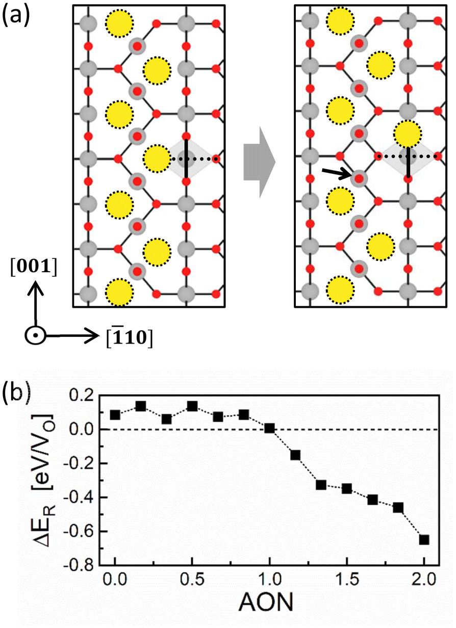 | ||
| Fig. 4 (a) Atomic-scale view of an initiation of the CF rupture process. The grey diamond represents the Ti–O octahedron, with the bold solid and dotted lines indicating the equatorial plane and the octahedral axis, respectively. For clarity, only the vicinity of the VOs is shown. (b) ΔER with respect to AON. Positive (negative) ΔER means that the rupture process is non-spontaneous (spontaneous). | ||
The first term on the right-hand side is the Ef for the ruptured CF (RCF, right panel of Fig. 4a), while the second is the Ef for the CF (left panel of Fig. 4a). Fig. 4b shows the variation of the ΔER as a function of AON. Thirteen AON values from 0 to +2 were considered with increments of 1/6, ensuring that the number of electrons in the supercell remains an integer. The sign of ΔER depends on the oxidation state and is positive up to AON of +1, which means that the rupture is not favored in the LO state. Conversely, the ΔER value becomes negative in the HO state (AON > +1), indicating the spontaneous rupture of the CF due to the repulsion between highly positively charged VOs.
To examine the charge distribution within the CF and RCF in the equilibrium state (no external bias is applied), the transition level diagrams (TLDs) were calculated, presenting the most stable AON as a function of the εf. Fig. 5a shows a schematic band diagram of a Pt/TiO2/Ti device based on the experimental values of the work functions of Pt (5.35 eV) and Ti (4.33 eV) and the electron affinity of TiO2 (4.0 eV).39–41 The range of εf available within a device is primarily influenced by the electrode materials. Accordingly, the possible range of εf values spans from 1.65 eV (near the Pt electrode) to 2.67 eV (near the Ti electrode).
 | ||
| Fig. 5 (a) Schematic band diagram of a Pt/TiO2/Ti system. The work function of Pt and Ti and the electron affinity of TiO2 are set to the experimental values. TLDs for (b) an isolated VO, (c) VOs in the CF, and (d) VOs in the RCF, where the x-axes are confined to the available range of εf in the Pt/TiO2/Ti system. (e) Atom-resolved DOS of the RCF (blue areas) when the AON is +1.33, obtained by the projection onto the Ti atom marked by an arrow in the right panel of Fig. 4a. For comparison, the DOS projected on the furthest Ti atom from the VOs, standing for the perfect rutile TiO2, is shown together as grey areas. | ||
Fig. 5b–d show the TLDs of an isolated VO, the CF, and the RCF, respectively, with the x-axes set to the available range of εf for this device. For the isolated VO, VO2+ is preferred across most εf regions, particularly in film regions near the Pt electrode, probably because oxygen ions prefer to be O2−. On the other hand, VO0 becomes predominant around the Ti electrode, which can supply additional VO0s to the nearby TiO2 from the Ti oxidation reaction. (See supplementary note 2 in the ESI† for oxygen ion exchange at the TiO2/Ti interface.) Considering that VO0s in proximity attract each other as described in section A, CF can readily be initiated at the TiO2/Ti interface, which may further grow toward the Pt electrode upon the set switching voltage application. For the CF in Fig. 5c, the LO state is preferred throughout all regions, indicating its stability across the film thickness. For the RCF in Fig. 5d, on the other hand, the HO state (AON = +1.33) becomes stable around the Pt electrode, while the LO state remains in other regions. Therefore, it can be inferred that the CF rupture may occur at the Pt/TiO2 interface when the reset voltage is applied. Meanwhile, the RCF in the LO state will spontaneously revert to the CF, following the energetic preference shown in Fig. 4b, preventing the CF from being wholly ruptured. Therefore, only a tiny portion of the CF near the Pt electrode, which prefers the HO state in the RCF, may play a crucial role in resistive switching. This finding is consistent with several high-resolution transmission electron microscopy (HRTEM) studies revealing that the CF of only a few nanometers in thickness participates in resistive switching.14,31,42 This local region involved in the resistive switching is called a CF tip in the remainder of this paper. These tendencies in TLDs demonstrate that the resistive switching is accompanied by charge transition of VOs: a decrease in AON during the CF formation and an increase in AON during the CF rupture process, as described in detail in the next section.
Fig. 5e shows the atom-resolved DOS of the RCF whose AON is +1.33, obtained by projecting onto the Ti ion marked by an arrow in Fig. 4a. The DOS projected on the Ti ion furthest from the VOs, standing for the perfect TiO2, was also represented as grey areas. Upon comparing with the DOS of the CF in Fig. 3e, the RCF is more resistive than the CF since there is no state crossing the Fermi level. This finding suggests that even a minor alternation of the arrangement of VOs can induce a significant change in the resistance.
C. Charge transition of VOs during the switching process
The source of the charge transition of VOs during the resistive switching is the charge injection by the applied bias (V). Fig. 6a represents the post-electroformed state with a tunneling gap between the Pt electrode and the CF (yellow trapezoid) when the device was electroformed with low electric power. When the Pt electrode is negatively biased, the injection of electrons (e−) from the Pt electrode is limited due to the tunneling gap with a high Schottky barrier height (SBH) at the Pt/TiO2 interface. In contrast, injecting holes (h+) from the Ti electrode is facilitated by the metallic contact between the CF and the Ti electrode. The charge transfer between the CF and the Ti electrode must be fluent since the Fermi level of the Ti electrode (0.33 eV under the CBM of TiO2) is located within the consecutive defect states of the CF (see Fig. 3e). Consequently, the h+ will accumulate at the CF tip, further oxidizing the VOs. This process was named h+-injection. Conversely, when the Pt electrode is positively biased, the e− will be injected from the Ti interface to the CF and accumulate at the CF tip, causing the reduction of VOs, which is named e−-injection. | ||
| Fig. 6 Overview of the switching process in the Pt/TiO2/Ti device. (a) The post-electroforming state characterized by a CF represented by the yellow trapezoid, along with a thin tunneling gap between the Pt electrode and the CF due to insufficient electric power. The dotted yellow circles represent the remaining VOs after the electroforming process. (b) Atomic structure of the CF tip in the pre-charge injection state. R, E, and I denote the released VO, VO located at the edge of the residual CF, and VO inside the residual CF, respectively. (c) Atomic structure of the CF tip after one movement of VO,R, corresponding to the RCF. Therefore, IM 1 represents the initiation of the CF rupture process from the structure in (b) to that in (c) (the same as Fig. 4a). (d) Atomic structure of the CF tip after subsequent movement of the VO,R. The VO,R drifts toward the upper right in response to the electric field and the concentration gradient of VO. (e) LRS of the device, where the VO2+s are located beneath the Pt electrode. The horizontal dotted arrows denote the CF rupture process, and the solid arrows indicate the CF rejuvenation process. The green and red bars at the bottom of the figure represent the ranges of the 8w and c8w BRS modes, respectively. | ||
The amount of charge carriers accumulated by V is determined by the capacitance (C) of the device. The upper limit of C was roughly estimated by assuming that the CFs are uniformly distributed across the entire cross-sectional area. In this case, the device geometry is a parallel plate capacitor whose electrodes are the CF and the Pt electrode; hence, C becomes εrε0A/t, where ε0, A, and t are the permittivity of vacuum, CF cross-sectional area, and spacing between the CF and the Pt electrode, respectively. As a result, the density of charge carriers (n) accumulated in the CF is given by n = Q/eΩCF, where Q is the total accumulated charge, given as εrε0AV/t, and ΩCF is the CF volume, given as A(l − t), where l is the total thickness of the TiO2 layer and e is the elementary charge. Therefore, we have n = εrε0V/et(l − t). Assuming that εr and l are the typical values of 100 and 10 nm, and V and t are 2 V and 1.5 nm based on an experiment by Zhang et al., the resulting n is estimated to be 8.67 × 1020 cm−3, which is about half the VO concentration of the suggested CF (1.82 × 1021 cm−3).11 Given that this n value is the upper limit, the actual change in the AON of the VOs by the charge injection will be modest. Therefore, the maximum change of AON due to charge injection from the equilibrium state was assumed to be ±0.5.
In this section, the effects of the charge injection on the switching behavior are addressed by examining the atomic kinetics and the evolution in the ION of each VO. With this purpose, the resistive switching process was simulated, where the evolution in the atomic structure of the CF tip is shown from Fig. 6b–d. Here, the IM indicates an ionic movement, and the dotted and solid arrows represent the rupture and the rejuvenation processes of the CF, respectively. During the rupture process indicated by IM 1 and IM 2, one VO denoted as R escapes and moves away from the CF. The remaining portion of the CF after releasing the VO is called residual CF. The rejuvenation process is the reverse process of the rupture. The three VOs, denoted as R, E, and I, are focused, where VO,R, VO,E, and VO,I indicate the released VO, the VO located at the edge of residual CF, and the VO inside the residual CF, respectively. The green and red bars at the bottom of the figure represent the ranges of the 8w and c8w BRS modes, which are discussed in sections C.1 and C.2, respectively.
C.1.1. 8w reset process. The CF exists in the LO state in an equilibrium state without an external bias, as depicted in Fig. 5c. However, when the Pt electrode is negatively biased, the VOs within the CF undergo additional oxidation by h+-injection. If the AON of the CF reaches the HO state, the CF will spontaneously rupture, as described in Fig. 6b and c (which are the same as that described in Fig. 4a), increasing the device resistance (reset switching). This charge transition-driven rupture process is triggered by a repulsive force between VOs in the HO state, distinguishing it from the conventional thermally induced rupture process. This charge transition-driven rupture process corresponds to the 8w reset process, as a negative voltage resets the device.
The AON of the CF tip was assumed to increase from the equilibrium state of +0.83 to +1.33 by h+-injection to simulate the charge transition-driven rupture process. The upper panel of Table 1 provides the energy gain (ΔE) and activation energy (Ea) for the rupture process (IM 1 and IM 2). The corresponding values for the diffusion of an isolated VO2+ are also shown together for comparison. (See Fig. S14† for a description of the VO2+ diffusion.) The IM 1 is expected to readily occur due to the large negative ΔE and the significantly lower Ea of 0.21 eV compared to VO2+ diffusion, 1.31 eV. After IM 1, the VO,R drifts toward the upper right direction in response to both the electric field and the concentration gradient of VO, as represented by IM 2 in Fig. 6. However, the Ea for IM 2, 1.34 eV, is much higher than that of IM 1. Considering the lack of operation power of the 8w BRS mode, IM 2 is unlikely to occur in the 8w BRS mode, making the 8w reset a two-step process consisting of the h+-injection and IM 1. Consequently, the device states in Fig. 6b and c become the low resistance state (LRS*) and the high resistance state (HRS*), respectively, of the 8w BRS mode. The asterisk is used to emphasize the involvement in the 8w BRS mode.
| Kinetic parameters | |||
|---|---|---|---|
| VO2+ diffusion | IM 1 | IM 2 | |
| ΔE [eV] | 0.00 | −2.15 | 0.00 |
| E a [eV] | 1.31 | 0.21 | 1.34 |
| Evolution in ION | ||||
|---|---|---|---|---|
| h+-injection | IM 1 | IM 2 | ||
| Pre- | Post- | |||
| VO,R | +0.83 | +1.33 | +2.03 | +2.07 |
| VO,E | +0.83 | +1.33 | +1.49 | +1.53 |
| VO,I | +0.83 | +1.33 | +0.93 | +0.96 |
The lower panel of Table 1 shows the evolution in IONs of three representative VOs. The whole dataset, including that of other VOs, is available in Table S1.† Before the h+-injection, the IONs are +0.83, corresponding to the equilibrium state of the CF near the Pt electrode, or the CF tip region, as shown in Fig. 5c. It increases to +1.33 after the h+-injection, as assumed. The IONs are the same because all VO-sites in the CF are symmetrically equivalent.
However, the IONs become dissimilar after IM 1. Most notably, the ION of VO,I changes from +1.33 to +0.93, indicating that the inside of the residual CF becomes the LO state from the HO state. Accordingly, the residual CF is expected to be stable. The following two events induce this charge transition. First, the excessive charge inside the CF is discharged by releasing VO,R in the further oxidized states. Note that the ION of VO,R becomes +2.03 after IM 1, then remains almost intact after IM 2. Furthermore, the kinetic parameters (ΔE and Ea) of VO,R for IM 2 are almost identical to those of VO2+ diffusion, suggesting that the VO,R behaves like an isolated VO2+ immediately after IM 1. Indeed, the cNEB profiles of these two processes are almost identical, as shown in Fig. S15.† For these reasons, IM 2 is identified with the VO2+ diffusion in this study. Consequently, it is concluded that the VO becomes VO2+ as soon as it is released from the CF. Second, charge redistribution occurs within the residual CF. Upon comparing the ION values of VO,E, and VO,I after IM 1, the remaining charge after releasing VO,R is concentrated at the edge of residual CF, reducing the charge inside the CF. This behavior is metal-like, which probably originates from the semi-metallic characteristic of the CF. However, the net charge remains inside because free carriers are insufficient to neutralize the internal charge due to the CF's relatively low density of defect states near the Fermi level, which differs from that of metal with zero internal charge. It should be noted that the charge transition-driven rupture process cannot be applied to the CF composed of the Magnéli phase Ti4O7 because no net charge exists within the Magnéli phase due to its fully metallic characteristic. In this case, the CF will be thermally ruptured, which requires high power consumption to overcome its superior stability.
Another 8w reset process was also simulated with the lower AON of +1.17. As shown in Table 2, similar results were obtained in both aspects that the VO,R behaves like an isolated VO2+ and that the charge redistribution within the residual CF occurs to reduce the internal charge. For IM 1, however, both ΔE and Ea are higher than the case of AON = +1.33, presumably due to the weaker repulsion between VO1.17+s compared to VO1.33+s. Nonetheless, the Ea value is still considerably lower than that for VO2+ diffusion, which accords with the low operation power of the 8w BRS mode.
| Kinetic parameters | |||
|---|---|---|---|
| VO2+ diffusion | IM 1 | IM 2 | |
| ΔE [eV] | 0.00 | −1.21 | −0.05 |
| E a [eV] | 1.31 | 0.78 | 1.30 |
| Evolution in ION | ||||
|---|---|---|---|---|
| h+-injection | IM 1 | IM 2 | ||
| Pre- | Post- | |||
| VO,R | +0.83 | +1.17 | +2.02 | +2.07 |
| VO,E | +0.83 | +1.17 | +1.51 | +1.52 |
| VO,I | +0.83 | +1.17 | +0.87 | +0.93 |
C.1.2. 8w set process. The atomic structure of the CF tip in HRS* is the same as that in the RCF. Hence, the AON of the ruptured CF tip is +1.33 (HO state) in an equilibrium state, as shown in Fig. 5d. However, when the Pt electrode is positively biased, the AON can decrease to the LO state due to e−-injection, resulting in spontaneous rejuvenation of the RCF to the CF, as represented by IM 3 in Fig. 6. This transition corresponds to the 8w set process (transition from HRS* to LRS*) since the positive voltage sets the device.
To simulate the charge transition-driven rejuvenation process, the AON of VOs in the ruptured CF tip was assumed to decrease from the equilibrium state of +1.33 to +0.83 by the e−-injection. Table 3 provides kinetic parameters for IM 3 (upper panel) in comparison with the diffusion of an isolated VO2+ and the evolution in IONs during the 8w set process (lower panel). The ION distribution before e−-injection is identical to that in IM 1 of Table 1. For the IM 3, ΔE is negative, and Ea is 0.66 eV, considerably lower than that of the VO2+ diffusion. Therefore, the 8w set can be driven with low electric power. Meanwhile, upon comparing IONs before and after the e−-injection, the ION of VO,R decreases from +2.03 to +1.03, and the ION of VO,E also decreases from +1.49 to +0.95. Since these two IONs are close to +1, an attractive force is expected between VO,R and VO,E after the e−-injection. Consequently, the main driving force of this rejuvenation process is the short-range attraction between VOs in the LO state rather than the Soret force induced by a temperature gradient, as conventionally explained.
| Kinetic parameters | ||
|---|---|---|
| VO2+ diffusion | IM 3 | |
| ΔE [eV] | 0.00 | −0.45 |
| E a [eV] | 1.31 | 0.66 |
| Evolution in ION | |||
|---|---|---|---|
| e−-injection | IM 3 | ||
| Pre- | Post- | ||
| VO,R | +2.03 | +1.03 | +0.83 |
| VO,E | +1.49 | +0.95 | +0.83 |
| VO,I | +0.93 | +0.86 | +0.83 |
Conversely, when a high positive voltage is applied to the Pt electrode, the reverse process, the c8w reset process, occurs, inducing VO2+s near the Pt electrode to move away from the electrode and drift toward the residual CF along the electric field. Subsequently, the ruptured CF will be rejuvenated by e−-injection, and the device will become the state of Fig. 6a. Due to the presence of the tunneling gap with a high SBH, the state of Fig. 6a is expected to be more resistive than LRS, and accordingly, this state corresponds to the high resistance state of the c8w polarity (HRS). Note that HRS is identical to LRS*, as shown in Fig. 1.
However, the explanations above still involve two ambiguous points. First, the CF rupture by h+-injection must precede the SBH lowering during the c8w set process, implying a temporary increase in resistance before it decreases. Indeed, this phenomenon was experimentally reported by Miao et al.,12 as discussed in the next section. Second, no quantitative explanation is provided for why the LRS in Fig. 6e is less resistive than the HRS in Fig. 6a. The change in resistance is determined by the competition between the tunneling gap thickening (increasing resistance) and the SBH lowering (decreasing resistance). However, the simulations of this variation are beyond the scope of DFT calculations due to the scale limitation. Qualitatively, according to the Schottky conduction equation in logarithmic form, ln(I) is proportional to t−1/2 but decreases linearly by SBH, indicating that the influence of the SBH lowering might be predominant over the thickening effect.44 Furthermore, the actual increase in thickness of the tunneling gap was insignificant, with a scale of 0.5 nm, based on the experiment of Zhang et al.11 Meanwhile, the additional contribution of VO2+s from the surroundings of the CF to the SBH lowering facilitates the decrease in resistance. Hence, the SBH lowering effect is expected to be predominant in the c8w set process, but a follow-up study is required to clarify this further.
 | ||
| Fig. 7 Summary of the proposed mechanism encompassing the 8w BRS mode (green bar) and the c8w BRS mode (red bar). The numerical values represent the Ea for the corresponding process in the unit of eV. The 8w BRS mode arises from the local redistribution of VOs within the CF tip, while the c8w BRS mode is caused by the mesoscopic redistribution of VOs between the Pt electrode and the CF tip. The 8w BRS mode can be driven by low electric power due to its significantly low Eas compared to the c8w BRS mode. | ||
The estimated Ea values support the experimental results that two direct transitions from HRS to LRS and from LRS to HRS* were not experimentally observed.12 In the former case, HRS was indirectly transformed to LRS, passing through HRS*. According to Fig. 7, the transition from HRS to LRS (from left to right panel) involves two sequential barriers of 0.21 eV and 1.31 eV. Since the first barrier is significantly lower than the second one, the device can easily overcome the first barrier but will remain in HRS* by the higher second barrier. For the transition from the LRS to HRS* (from right to middle panel), on the other hand, the device in HRS*, which has surpassed the barrier of 1.31 eV, can easily overcome the subsequent barrier of 0.66 eV, resulting in an immediate transition to HRS. Hence, the transition from the LRS to HRS* is not observable.
It should be noted that these claims are based on a straightforward observation that attractive and repulsive forces occur between VOs in the LO and HO states, respectively. Accordingly, these findings may hold for other materials showing similar behaviors. Indeed, similar tendencies in the interaction between VOs were reported in various VCM materials, such as Ta2O5, HfO2, and Al2O3.7,46,47 Consequently, these findings are expected to apply to various VCM devices.
While this study focused only on rutile TiO2, TiO2 films in real devices are commonly polycrystalline or amorphous. To address this limitation, the Ecoh in anatase TiO2, another major phase, was also calculated, as shown in Fig. S16.† The tendency in Ecoh is similar to rutile TiO2, implying that the findings can be similarly applied to anatase TiO2.45
4. Conclusion
An improved resistive switching mechanism considering the charge transition and the atomic kinetics of VO is suggested to explain the coexistence of the 8w and c8w BRS modes in the Pt/TiO2/Ti model device. The suggested mechanism gives enhanced insights into the resistive switching process as follows. First, the CF prefers to be composed of VOs in the low oxidation state (LO state) rather than those in the high oxidation state (HO state), which contrasts with the prior simulation studies that considered the CF an aggregation of VO2+s. The stability of the CF in the LO state arises from a short-range attraction between VOs in the LO state. Second, the 8w BRS mode is charge transition-driven switching, where the attraction at the LO state and repulsion at the HO state cause the CF rejuvenation (8w set) and rupture (8w reset) processes, respectively. These charge transition-driven switchings exhibit lower activation barriers ranging from 0.21 eV–0.78 eV (depending on the oxidation number (ON)) compared to the conventional field-driven switching, whose activation barrier is 1.31 eV. It enables the 8w BRS mode to operate with low electric power. Lastly, a VO released from the CF becomes VO2+ only by one ionic movement, indicating that the charge transition of VO occurs within a localized region near the CF. Given that the c8w BRS mode occurs throughout a broad region compared to the 8w BRS mode, the influence of the charge transition of VO on the switching behavior of c8w polarity is negligible. Therefore, limited to the c8w BRS mode, fixing ON of VO to +2, as in previous studies, can provide a plausible interpretation for resistive switching.Author contributions
Taeyoung Jeong: formal analysis, investigation, methodology, and writing – original draft; In Won Yeu: formal analysis and writing – review & editing; Kun Hee Ye: formal analysis and writing – review & editing; Seungjae Yoon: formal analysis and writing – review & editing; Dohyun Kim: writing – review & editing; Cheol Seong Hwang: supervision and writing – review & editing; Jung-Hae Choi: conceptualization, funding acquisition, project administration, supervision, and writing – review & editing.Conflicts of interest
The authors declare that they have no known competing financial interests or personal relationships that could have appeared to influence the work reported in this paper.Acknowledgements
J.-H. C. was supported by the National Research Foundation of Korea (NRF) grant funded by MSIT [Next Generation Intelligence Semiconductor Foundation 2022M3F3A2A01076569], and by the Institutional Research Program of Korea Institute of Science and Technology (KIST) [2E32491 and 2E33223]. C. S. H. was supported by the National Research Foundation of Korea [2020R1A3B2079882]. The authors would also like to acknowledge the support from the KISTI Supercomputing Center through a Strategic Support Program for Supercomputing Application Research [KSC-2022-CRE-0378].References
- Y. H. Jang, S. H. Lee, J. Han, W. Kim, S. K. Shim, S. Cheong, K. S. Woo, J.-K. Han and C. S. Hwang, Adv. Mater., 2023, 2309314 Search PubMed.
- T. Stecconi, R. Guido, L. Berchialla, A. L. Porta, J. Weiss, Y. Popoff, M. Halter, M. Sousa, F. Horst, D. Dávila, U. Drechsler, R. Dittmann, B. J. Offrein and V. Bragaglia, Adv. Electron. Mater., 2022, 8, 2200448 CrossRef CAS.
- D. S. Jeong, K. M. Kim, S. Kim, B. J. Choi and C. S. Hwang, Adv. Electron. Mater., 2016, 2, 1600090 CrossRef.
- R. Waser, R. Dittmann, G. Staikov and K. Szot, Adv. Mater., 2009, 21, 2632–2663 CrossRef CAS PubMed.
- K. M. Kim, B. J. Choi, Y. C. Shin, S. Choi and C. S. Hwang, Appl. Phys. Lett., 2007, 91, 012907 CrossRef.
- K. Kamiya, M. Y. Yang, S.-G. Park, B. Magyari-Köpe, Y. Nishi, M. Niwa and K. Shiraishi, Appl. Phys. Lett., 2012, 100, 073502 CrossRef.
- J. Lee, W. Schell, X. Zhu, E. Kioupakis and W. D. Lu, ACS Appl. Mater. Interfaces, 2019, 11, 11579–11586 CrossRef CAS PubMed.
- J. Park, J. Choi, G. Kim, G. Kim, G. S. Kim, H. Song, Y. S. Kim, Y. Lee, H. Rhee, H. M. Lee, C. S. Hwang and K. M. Kim, ACS Appl. Mater. Interfaces, 2022, 14, 35949–35958 CrossRef CAS PubMed.
- R. Muenstermann, T. Menke, R. Dittmann and R. Waser, Adv. Mater., 2010, 22, 4819–4822 CrossRef CAS PubMed.
- X.-B. Yin, K. Tian, Z.-H. Tan, R. Yang and X. Guo, J. Electrochem. Soc., 2015, 162(10), E271–E275 CrossRef CAS.
- H. Zhang, S. Yoo, S. Menzel, C. Funck, F. Cüppers, D. J. Wouters, C. S. Hwang, R. Waser and S. Hoffmann-Eifert, ACS Appl. Mater. Interfaces, 2018, 10, 29766–29778 CrossRef CAS PubMed.
- F. Miao, J. J. Yang, J. Borghetti, G. Medeiros-Ribeiro and R. S. Williams, Nanotechology, 2011, 22, 254007 CrossRef PubMed.
- K. M. Kim, G. H. Kim, S. J. Song, J. Y. Seok, M. H. Lee, J. H. Yoon and C. S. Hwang, Nanotechology, 2010, 21, 305203 CrossRef PubMed.
- Y. Zhang, G.-Q. Mao, X. Zhao, Y. Li, M. Zhang, Z. Wu, W. Wu, H. Sun, Y. Guo, L. Wang, X. Zhang, Q. Liu, H. Lv, K.-H. Xue, G. Xu, X. Miao, S. Long and M. Liu, Nat. Commun., 2021, 12, 7232 CrossRef CAS PubMed.
- D. Cooper, C. Baeumer, N. Bernier, A. Marchewka, C. L. Torre, R. E. Dunin-Borkowski, S. Menzel, R. Waser and R. Dittmann, Adv. Mater., 2017, 29, 1700212 CrossRef PubMed.
- T. Heisig, C. Baeumer, U. N. Gries, M. P. Mueller, C. L. Torre, M. Luebben, N. Raab, H. Du, S. Menzel, D. N. Mueller, C.-L. Jia, J. Mayer, R. Waser, I. Valov, R. A. D. Souza and R. Dittmann, Adv. Mater., 2018, 30, 1800957 CrossRef PubMed.
- A. Schönhals, C. M. M. Rosário, S. Hoffmann-Eifert, R. Waser, S. Menzel and D. J. Wouters, Adv. Electron. Mater., 2018, 4, 1700243 CrossRef.
- H. Ryu and S. Kim, Nanomaterials, 2020, 10, 2055 CrossRef CAS PubMed.
- G. Kresse and J. Furthmüller, Phys. Rev. B: Condens. Matter Mater. Phys., 1996, 54, 11169–11186 CrossRef CAS PubMed.
- G. Kresse and J. Furthmüller, Comput. Mater. Sci., 1996, 6, 15–50 CrossRef CAS.
- D. M. Ceperley and B. J. Alder, Phys. Rev. Lett., 1980, 45, 566–569 CrossRef CAS.
- J. P. Perdew and A. Zunger, Phys. Rev. B: Condens. Matter Mater. Phys., 1981, 23, 5048–5079 CrossRef CAS.
- S. L. Dudarev, G. A. Botton, S. Y. Savrasov, C. J. Humphreys and A. P. Sutton, Phys. Rev. B: Condens. Matter Mater. Phys., 1998, 57, 1505 CrossRef CAS.
- D. T. Cromer and K. Herrington, J. Am. Chem. Soc., 1955, 77, 4708–4709 CrossRef CAS.
- D. Reyes-Coronado, G. Rodríguez-Gattorno, M. E. Espinosa-Pesqueira, C. Cab, R. d. Coss and G. Oskam, Nanotechnology, 2008, 19, 145605 CrossRef CAS PubMed.
- A. Janotti, J. B. Varley, P. Rinke, N. Umezawa, G. Kresse and C. G. Van de Walle, Phys. Rev. B: Condens. Matter Mater. Phys., 2010, 81, 0852121 CrossRef.
- A. Malashevich, M. Jain and S. G. Louie, Phys. Rev. B: Condens. Matter Mater. Phys., 2014, 89, 075205 CrossRef.
- G. Henkelman, A. Arnaldsson and H. Jónsson, Comput. Mater. Sci., 2006, 36, 354 CrossRef.
- G. Henkelman and H. Jónsson, J. Chem. Phys., 2000, 113, 9901–9904 CrossRef CAS.
- G. Henkelman and H. Jónsson, J. Chem. Phys., 2000, 113, 9978–9985 CrossRef CAS.
- D.-H. Kwon, K. M. Kim, J. H. Jang, J. M. Jeon, M. H. Lee, G. H. Kim, X.-S. Li, G.-S. Park, B. Lee, S. Han, M. Kim and C. S. Hwang, Nat. Nanotechnol., 2010, 5, 148–153 CrossRef CAS PubMed.
- Y. M. Lu, M. Noman, Y. N. Picard, J. A. Bain, P. A. Salvador and M. Skowronski, J. Appl. Phys., 2013, 113, 163703 CrossRef.
- K. Zhang, Y. Ren, P. Ganesh and Y. Cao, npj Comput. Mater., 2022, 8, 76 CrossRef CAS.
- T. Li, F. Hong, K. Yang, B. Yue, N. Tamura, H. Wu, Z. Cheng and C. Wang, Sci. Bull., 2020, 65, 631–639 CrossRef CAS PubMed.
- M. Domaschke, X. Zhou, L. Wergen, S. Romeis, M. E. Miehlich, K. Meyer, W. Peukert and P. Schmuki, ACS Catal., 2019, 9, 3627–3632 CrossRef CAS.
- M. Chandran, Comput. Mater. Sci., 2015, 108, 192–204 CrossRef CAS.
- W. Heckel, M. Wehlau, S. B. Maisel, T. Frauenheim, J. M. Knaup and S. Müller, Phys. Rev. B: Condens. Matter Mater. Phys., 2015, 92, 214104 CrossRef.
- B. Magyari-Köpe, S. G. Park, H.-D. Lee and Y. Nishi, J. Mater. Sci., 2012, 47, 7498–7514 CrossRef.
- R. Vanselow and X. Q. D. Li, Surf. Sci. Lett., 1992, 264, L200–L206 CrossRef CAS.
- D. R. Lide, CRC Handbook of Chemistry and Physics, CRC Press, Boca Raton, FL, 2014, pp. 12–124 Search PubMed.
- X. Yin, C. Battaglia, Y. Lin, K. Chen, M. Hettick, M. Zheng, C.-Y. Chen, D. Kiriya and A. Javey, ACS Photonics, 2014, 1, 1245–1250 CrossRef CAS PubMed.
- J.-Y. Chen, C.-L. Hsin, C.-W. Huang, C.-H. Chiu, Y.-T. Huang, S.-J. Lin, W.-W. Wu and L.-J. Chen, Nano Lett., 2013, 13, 3671–3677 CrossRef CAS PubMed.
- J. J. Yang, J. Borghetti, D. Murphy, D. R. Stewart and R. S. Williams, Adv. Mater., 2009, 21, 3754–3758 CrossRef CAS.
- C.-R. Cheng, M.-H. Tsai, T.-H. Hsu, M.-J. Li and C.-L. Huang, J. Alloys Compd., 2023, 930, 167487 CrossRef CAS.
- T. Lee and A. Selloni, J. Phys. Chem. C, 2023, 127(1), 627–634 CrossRef CAS.
- K. Kamiya, M. Y. Yang, T. Nagata, S.-G. Park, B. Magyari-Köpe, T. Chikyow, K. Yamada, M. Niwa, Y. Nishi and K. Shiraishi, Phys. Rev. B: Condens. Matter Mater. Phys., 2013, 87, 155201 CrossRef.
- M. Y. Yang, K. Kamiya, B. Magyari-Köpe, H. Momida, T. Ohno, M. Niwa, Y. Nishi and K. Shiraishi, Jpn. J. Appl. Phys., 2013, 52, 04CD11 CrossRef.
Footnote |
| † Electronic supplementary information (ESI) available. See DOI: https://doi.org/10.1039/d3nr06614b |
| This journal is © The Royal Society of Chemistry 2024 |