
Defects in lead halide perovskite light-emitting diodes under electric field: from behavior to passivation strategies
Na
Jiang
ab,
Guoquan
Ma
ab,
Dandan
Song
 ab,
Bo
Qiao
ab,
Zhiqin
Liang
ab,
Zheng
Xu
*ab,
Swelm
Wageh
c,
Ahmed
Al-Ghamdi
c and
Suling
Zhao
*ab
ab,
Bo
Qiao
ab,
Zhiqin
Liang
ab,
Zheng
Xu
*ab,
Swelm
Wageh
c,
Ahmed
Al-Ghamdi
c and
Suling
Zhao
*ab
aKey Laboratory of Luminescence and Optical Information, Beijing Jiaotong University, Ministry of Education, Beijing, 100044, China. E-mail: zhengxu@bjtu.edu.cn; slzhao@bjtu.edu.cn
bInstitute of Optoelectronics Technology, Beijing Jiaotong University, Beijing, 100044, China
cDepartment of Physics, Faculty of Science, King Abdulaziz University, Jeddah 21589, Saudi Arabia
First published on 30th January 2024
Abstract
Lead halide perovskites (LHPs) are emerging semiconductor materials for light-emitting diodes (LEDs) owing to their unique structure and superior optoelectronic properties. However, defects that initiate degradation of LHPs through external stimuli and prompt internal ion migration at the interfaces remain a significant challenge. The electric field (EF), which is a fundamental driving force in LED operation, complicates the role of these defects in the physical and chemical properties of LHPs. A deeper understanding of EF-induced defect behavior is crucial for optimizing the LED performance. In this review, the origins and characterization of defects are explored, indicating the influence of EF-induced defect dynamics on LED performance and stability. A comprehensive overview of recent defect passivation approaches for LHP bulk films and nanocrystals (NCs) is also provided. Given the ubiquity of EF, a summary of the EF-induced defect behavior can enhance the performance of perovskite LEDs and related optoelectronic devices.
 Na Jiang | Na Jiang received her B.S. from Hebei University in 2020. Now, she is a Ph.D. candidate in Optical Engineering at Beijing Jiaotong University, under the supervision of Professor Zheng Xu. Her current research focuses on optoelectronic devices based on metal halide perovskites. |
 Zheng Xu | Zheng Xu works in the Beijing Jiaotong University as a physics professor since 2005. He got his Ph.D. in 2002 at the Graduate School of the Chinese Academy of Sciences with a major in condensed matter physics. In 1996, he joined the Institute of Optoelectronic Technology, Beijing Jiaotong University as a senior engineer. His research interests are optoelectronic materials and devices, flat panel display technology, solar cells, semiconductor lighting, and nanomaterials. |
 Suling Zhao | Suling Zhao works in the Beijing Jiaotong University as a physics professor since 2011. She got her Ph.D. in 2003 at Northern Jiaotong University with a major of luminescence, then she finished her postdoc works in Tohoku University of Japan and Paris Sud University of France. In 2005, she joined the Institute of Optoelectronic Technology, Beijing Jiaotong University as an associate professor. Her research interests are luminescence nanomaterials and devices, electroluminescence devices, and solar cells. |
1. Introduction
Over the past decade, lead halide perovskites (LHPs) have garnered substantial attention owing to their remarkable optoelectronic properties, including exceptional color purity,1 tunable optical bandgaps,2 robust defect tolerance,3,4 narrow emission linewidths,1 wide color gamut,2 high charge-carrier mobility,5 and elevated photoluminescence quantum yield (PLQY).6 Consequently, LHPs have found widespread applications in various optoelectronic devices, such as photovoltaics, light-emitting diodes (LEDs), nanolaser, and photodetectors.3,7,8 In 2014, Tan et al. first realized near-infrared, red, and green electroluminescence (EL) devices based on perovskite at room temperature.9 Subsequently, there has been a significant increase in the external quantum efficiency (EQE) of perovskite light-emitting diodes (PeLEDs), with red, green, and blue PeLEDs reaching 26.3%,10 30.84%,11 18.65%,12 respectively, within a relatively short time frame. Numerous studies have focused on the investigation of defects in perovskite materials, which have emerged as a recurring focal point for enhancing device performance and stability.Similar to traditional colloidal quantum dot light-emitting diodes (QLEDs) and organic light-emitting diodes (OLEDs), the solution-based processability inherent in PeLEDs inevitably generates defects, which, in the context of PeLEDs, are pivotal factors influencing their commercial feasibility. Nanocrystals (NCs) and thin films from the perovskite family frequently feature intrinsic, grain boundary, and interface defects.13 Shallow-level defects, typically originating from inherent point defects, serve as carrier traps to capture electrons and holes, thereby creating avenues for energy loss.14 Even though LHPs are acknowledged for their high “defect tolerance”, diverse defects can induce alterations in the energy band of the emitting layer (EML), resulting in energy band misalignment.15 Moreover, deep-level defects commonly form centers for nonradiative recombination, disrupting charge transport and impacting carrier lifetime and PLQY.16 Defects are the fundamental origin of ion migration. The phenomenon of ion migration, driven by point defects and grain boundary defects, leads to phase separation, shifts in EL peak position, and device instability.17 In light of these considerations, we posit that a more profound understanding and controlled manipulation of defect behaviors hold the potential to significantly enhance the performance of PeLEDs, particularly in terms of EQE and stability.
In addition to defect physics, defect behavior under an inevitable electric field (EF) has exhibited another impact that requires serious consideration. Generally, defects can transform into “charged defects” under sustained EF, resulting in free carrier-like motion, particularly in halide vacancies associated with ion migration. Ion migration poses a real obstacle to the stability and ageing of perovskites. First-principles calculations with increasing EF have verified alterations in lattice structures, including lattice parameters, band gaps, and light absorption properties.19 The influence of EF on the interaction between charged defects and photoexcited species leads to temperature-dependent changes in the PL yield and decay.20 Furthermore, the migration of charged defects can undergo redox reactions, producing new defects under bias, subsequently leading to new nonradiative centers detrimental to the PeLEDs.21 Nevertheless, the intricacies of defect behavior under active EF remain generally undefined, indicating an urgent need for comprehensive exploration.
In this review, we presented a comprehensive discussion of the origin, characterization, and behavior of defects under EF and their passivation in PeLEDs, as depicted in Fig. 1. We began by elucidating the significance of defects, delving into their nature, classification, and characterization within perovskites. Subsequently, we presented several current perspectives on the defect behavior under EF. Based on the damage posed by field-induced defect behavior, we outlined the latest strategies for defect passivation and regulation to enhance the stability and efficiency of PeLEDs. We concluded by discussing current theories on defect behavior and highlighting avenues for future research.
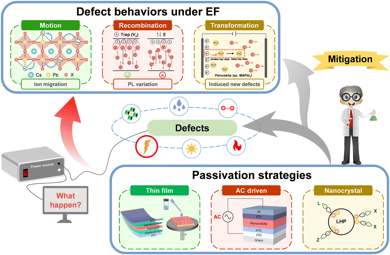 | ||
| Fig. 1 Schematic summary of EF-induced defect behaviors and passivation strategies in PeLEDs. | ||
2. Significance of defects
The defect state density in lead-based perovskites has been reported to range from 1010 to 1018 cm−3.22 The presence of these defects compromise device performance, impeding the commercial potential of perovskite devices.2.1 Fundamental characteristics of LHPs
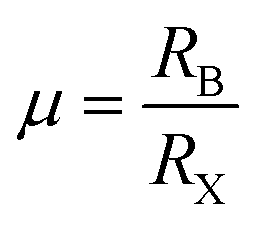
Crystalline LHPs conform to the ABX3 chemical stoichiometry: ‘A’ signifies a monovalent cation such as CH3NH3+ (MA+), CH(NH2)2+ (FA+), or Cs+; ‘B’ denotes a divalent metal cation, typically Pb2+ or Sn2+; and ‘X’ represents a halide anion, usually Cl−, Br−, or I−. The octahedral [BX6]4− consists of six halide anions coordinating with the B-site cation, and the extended framework of the corner-sharing [BX6]4− octahedrons encloses a cuboctahedral void filled by the larger A cation, as shown in Fig. 2a.23 Three standard crystal structures, α (cubic), β (tetragonal), and γ (orthorhombic), are associated with the extent of the [BX6]4− octahedron tilt, as illustrated in Fig. 2b. The A-site cation forms ionic bonds with [BX6]4− octahedra, bestowing LHPs with distinctive electron-ionic properties and a softer lattice than other traditional semiconductors. The Goldschmidt tolerance factor (t) and octahedral factor (μ) were used to assess the stability of the LHP lattice.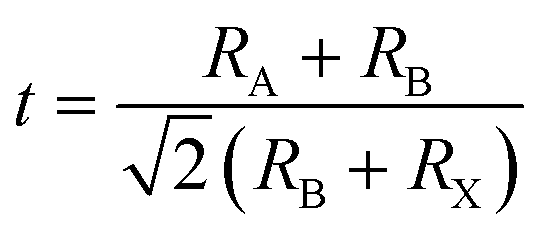 | (1) |
 | (2) |
 | (3) |
 | ||
| Fig. 2 (a) Schematic diagram of perovskite crystal structure. Reproduced with permission from ref. 23. Copyright 2014 Springer Nature. (b) Crystal structures of different phases of APbX3. Reproduced with permission from ref. 27. Copyright 2021 AIP Publishing. (c) Formation energies of native defects under three representative growth conditions. (d) Thermodynamic equilibrium range of the perovskite MAPbI3 growth conditions. (c and d) Reproduced with permission from ref. 28. Copyright 2021 Springer Nature. (e) Schematic dynamic processes at low excitation (left) and high excitation (right), involving defect trapping and detrapping, which determine the PL increment, and ion activation, migration, and accumulation, which determine the PL quenching. Reproduced with permission from ref. 32. Copyright 2016 Wiley-VCH. (f) Extracted device surface temperature against time curve (left) and photographs of a completed PeLED device (top) and a perovskite film covered by TPBi and LiF (bottom) subjected to annealing at different temperatures under 365 nm UV lamp illumination. Reproduced with permission from ref. 37. Copyright 2013 Royal Society of Chemistry. | ||
2.2 Origin of defects
An impressive cost-efficiency ratio is one of the most significant advantages of LHPs. However, utilizing a low-cost solution-based method invariably renders the control of the nucleation and growth challenging, leading to the inherent formation of defects. Eqn (4) describes the formation energy ΔH(α, q) for defect α in its charge state q.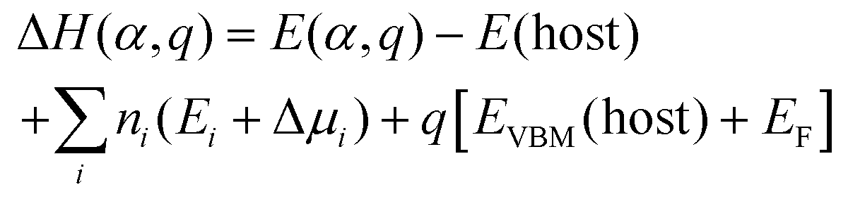 | (4) |
In this equation, the energy difference between the two systems is defined by the total energy E(α, q) of a supercell with a defect at the charge state q and the inherent energy E(host) of an identical supercell devoid of the defect. The ni and μi represent the number of atoms and atomic chemical potential, respectively, with q signifying the electron charge. Ei denotes the atomic energy of species i, and EF represents the Fermi energy level. It should be noted that eqn (4) is applicable to thin-film materials, whereas defect formation in NCs adheres to the subsequent framework,
| ΔHNCf(α + α′) = E[NC(α + α′)] − E(NC) ± E(s) | (5) |
However, the origin of these defects is intricate. Overall, defect origins can be classified into inherent and external stimulation.
Beyond the ambient air environment, external stimulation, such as sustained illumination, EF, and thermal field can intensify interactions with defects. Overall, the influence of field-induced defects in PeLEDs is complex and depends on defect density, material attributes, and environmental circumstances. Illumination has been identified as a factor that modifies the optoelectronic characteristics of perovskites and their devices. The PL of perovskite presents improvement, quenching, or remain constant under continuous illumination, depending on the density of intrinsic defect states in films produced by different methodologies, as illustrated in Fig. 2e.32 An increase in PL implies defect de-trapping to a certain degree through curing under illumination, whereas a constant PL indicates ongoing saturation. Illumination exposure can lead to the emergence of photo-induced defects, which trap charge carriers, reducing device efficiency.33 Additionally, light can induce ion migration, resulting in charge redistribution in the EML, a phenomenon that partially reverses in darkness.34 Quilettes et al. concluded that the PL enhancement in dimmer grains considerably surpassed that in bright grains, due to iodide redistribution. In actual experiments, light and oxygen frequently co-influence devices. This is evident when MAPbI3 degrades upon simultaneous exposure to light and oxygen through the formation of superoxide species.35
Joule heating is a crucial aspect in the operation of electroluminescent devices. However, a deeper understanding of its impact on PeLEDs stability remains elusive. Joule heating is associated with thermally activated ion migration and can inflict irreversible damage to the organic transport layer or interfaces.36,37 Under a bias voltage of 6 V, the device can attain temperatures approaching 70 °C, as shown in Fig. 2f. In comparison, inorganic perovskites exhibit superior thermal stability compared to their organic–inorganic hybrid counterparts. Moreover, various temperatures cause phase transitions in perovskites. For CsPbCl3, the transition temperatures from monoclinic to orthorhombic to tetragonal are 37 °C, 42 °C, and 47 °C,38 respectively. Similar behaviors are observed in CsPbBr3 and CsPbI3.39,40
EF is more than a primary driving force of device operation, requiring a higher level of attention. Although current research on the influence of EFs on perovskite optoelectronic devices has predominantly focused on photovoltaics, LEDs remain understudied. Similar to the influence of illumination on perovskite materials, EFs also trigger ion migration and phase separation, leading to an increase in defects and degradation of the crystal structure.41 The ionic properties of the octahedral “sub-lattice” within the perovskite framework facilitate the mobility of both positive and negative charged ions or vacancies under EF,42 particularly VX defects,43 which behave akin to free carriers under sustained EF. In addition, EF can introduce new defects and alter the energy band structure. Studying the effect of EF on defect behavior remains limited, and will be the focal point of the ensuring chapter.
2.3 Classification of defects
As mentioned previously, defects can be caused by numerous sources and occur in a diverse range of types. Understanding these specific defect types facilitates identification of their origins and underlying formation mechanisms, enabling effective characterization and regulation. Based on distinct classification standards, these defects can be categorized as follows.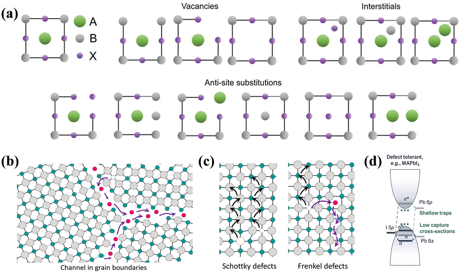 | ||
| Fig. 3 (a) Scheme of vacancies, interstitials and anti-site substitutions in the perovskite lattice. Reproduced with permission from ref. 44. Copyright 2022 Wiley-VCH. (b) Open spaces and dislocations at grain boundaries. (c) Illustration of Schottky defects (left) and Frenkel defects (right). (b and c) Reproduced with permission from ref. 45. Copyright 2016 American Chemical Society. (d) Electronic structure of defect-tolerant materials (e.g. MAPbI3), which primarily form shallow traps with low capture cross-sections. Reproduced with permission from ref. 13. Copyright 2021 Wiley-VCH. | ||
2.4 Advanced characterizations of EF-induced defect behaviors
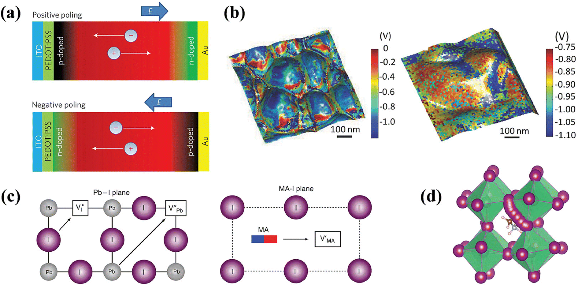
It is highly practical to reveal the behavior of defects in metal halide PeLEDs, as it is closely correlation with the device performance and optoelectronic properties. To date, there have been few characterization techniques employed to directly identify defect states. In addition, most defect behavior assessments are typically inferred from variations in the device performance, either enhancement or degradation. As previously mentioned, defects range from low- to high-dimensional types, arising from internal or environmental factors. Device performance parameters shift as the defect density is reduced through passivation or ligand-engineering strategies. This section summarizes the pivotal methods for characterizing defect behaviors, including microscopic, spectroscopic, and electrical measurements, and elucidates how these methods assess defect status alterations caused by minimized nonradiative losses. The manner in which these characterizations with defects deserves further study.Kelvin probe force microscopy (KPFM). KPFM, a derivative of AFM, is a non-contact technique for measuring the surface potential. It leverages the potential difference between the probe and the sample surface to obtain the surface potential distribution,52 which is an indirect method to characterize the presence and nature of defects. By initially mapping the surface topography with AFM and maintaining a fixed probe height, the potential difference, VCPD, between the probe and the sample surface can be determined.53 KPFM measures the electrostatic forces of samples using an externally applied alternating voltage (VAC) and bias (VDC), generating a surface potential map. In Fig. 4a, increased VCPD at grain boundaries emerged under positive voltage from defect-induced ion accumulation, while efficient ion extraction under negative voltage reduced VCPD.54 However, it should be noted that variations in surface potential may not only originate from hole or electron traps affecting the local charge distribution but also be influenced by the chemical composition of the material, surface roughness, other electronic effects, environmental conditions, and so on. It is often necessary to combine other characterizations to analyze defect states accurately.
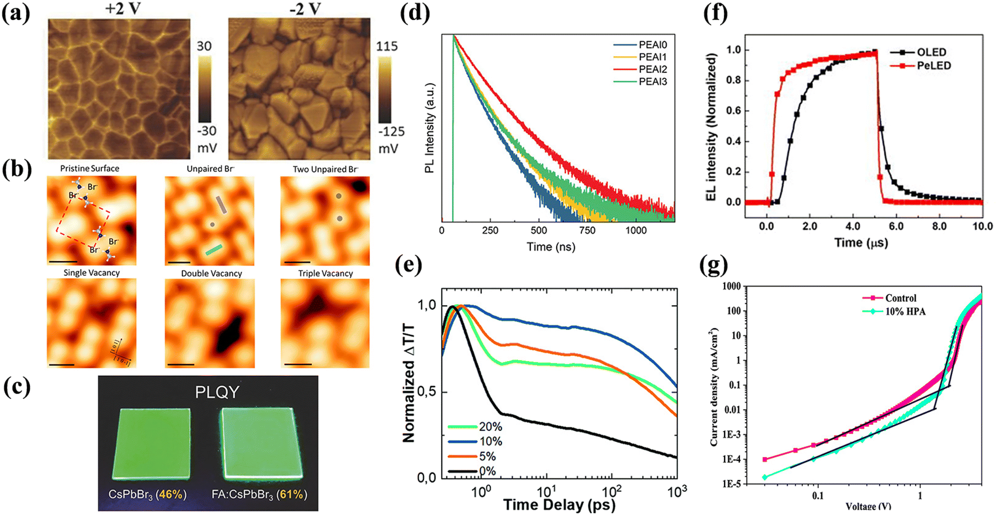 | ||
| Fig. 4 (a) CPD mapping images in the dark after applying positive bias (left) and negative bias (right). Reproduced with permission from ref. 54. Copyright 2016 Wiley-VCH. (b) Intrinsic defects on the surface of MAPbBr3 monitored by STM. Reproduced with permission from ref. 57. Copyright 2019 American Chemical Society. (c) Highly luminescent, smooth, and compact NC films, featuring a photograph of high bright CsPbBr3 and FA-doped CsPbBr3 NC films. Reproduced with permission from ref. 59. Copyright 2018 Wiley-VCH. (d) TrPL decay curves of FAPbI3 NCs treated with various PEAI concentrations. Reproduced with permission from ref. 62. Copyright 2022 Wiley-VCH. (e) Comparison of initial carrier recombination of CsPb1−xMgxBr3 perovskite films with different MgBr2 concentrations deposited directly on quartz. Reproduced with permission from ref. 65. Copyright 2016 Royal Society of Chemistry. (f) TrEL of OLED and PeLED at the 5 V. Reproduced with permission from ref. 72. Copyright 2019 AIP Publishing. (g) Current density–voltage characteristics of hole-dominated devices with a control perovskite or 10% HPA layer. Reproduced with permission from ref. 75. Copyright 2022 American Chemical Society. | ||
Scanning tunneling microscopy (STM). This high-resolution technique enables visualization of surface structures at the atomic scale, capturing both the electronic and morphological attributes of LHPs.55 When integrated with density functional theory (DFT), it elucidates surface and sub-surface structures, accentuating the interface properties. For a tunneling current to be obtained, probe-to-surface distance should be less than 1 nm.56 As Stecker et al. revealed that in MAPbBr3, single unpaired Br− was caused by pair orientation mismatches and, with the assistance of vacancies, further associate with Br neighbors to form two unpaired Br−.57 Moreover, single, double, and triple vacancies could be clearly appeared as dark depression at atomic scale in STM images (Fig. 4b). In STM testing, the preparation and cleanliness of the sample surface significantly impact the measurement results, and care should be taken to identify artifacts caused by changes in local charge distribution due to inhomogeneous sample surfaces or contamination. When comparing test results side-by-side, attention should be paid to probing information, scanning parameters, etc.
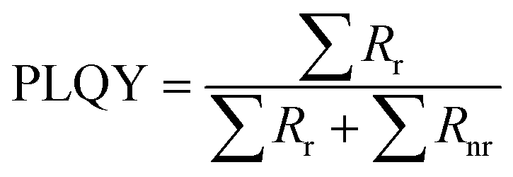
Photoluminescence quantum yield (PLQY). Generally, the PLQY is a key parameter affected by carrier recombination kinetics in LHPs, which can be described as the quotient of the radiative recombination rates to the rates of overall recombination in eqn (6):5
 | (6) |
 | (7) |
 | (8) |
Time-resolved photoluminescence (TrPL). TrPL is a transient decay assessment method used to analyze charge carrier recombination dynamics, indirectly indicating the extent of defect formation in NCs or films. Typically, the TrPL decay is modeled using the rate equation:5,60
 | (9) |
 | (10) |
Transient absorption spectroscopy (TA). TA spectroscopy, also known as ultrafast transient absorption or pump–probe technology, has been employed to investigate the carrier transport dynamics in bulk perovskite materials or films. This provides insights into charge extraction from device interfaces and energy transfer from excited states. The nomenclature “pump–probe” arises from the dual-pulse measurement technique involving distinct pump and probe pulses. The regenerative amplifier generates a pulse beam that is subsequently bifurcated. The majority of the beam serves as the pump pulse, while a lesser fraction is converted into weak broadband white light, designated as the probe pulse.61 Both the high-energy pump beam and broadband white light probe beam sequentially irradiate the sample. This transition shifts the sample from the ground state to an excited state upon pump-light excitation. Therefore, TA spectroscopic measurements commonly comprise signals from excited state absorption (ESA), ground-state bleaching (GSB), and stimulated emission (SE).63 The TA curve captures both the detection and reference light signals, with or without the pump pulse, and includes ΔA and ΔT signals. The ΔA signal, which is calculated as the difference in absorption spectrum between the excited and ground states, can manifest as either a positive or negative value. This signal serves to probe the temporal evolution of photoexcited states,63
 | (11) |
TA spectroscopy is a powerful tool for monitoring carrier relaxation by capturing variation data in light absorption or reflection in time and space, which is enabled by the interplay between pump and the probe light pulses. This method has revolutionized the study of microscopic defect dynamics in various optoelectronic devices, including photovoltaics, LEDs, and optoelectronic detectors. Nevertheless, choosing different excitation intensities and wavelength conditions produces varying results regarding the intensity and dynamics of the TA signal. Sample treatment (e.g., preparation method, film thickness) and testing environment (e.g., temperature, atmospheric conditions) before TA tests also affect results. Researchers should exclude nonlinear effects and sample degradation as much as possible before interpreting TA signals. Sun et al. demonstrated a reduction in defect density in CsPbBr3 perovskite by partially substituting Mg2+ for Pb2+, as confirmed through TA spectroscopy and TrPL.65 As shown in Fig. 4e, the incorporation of Mg2+ led to a slower relaxation rate of the initial peak upon photoexcitation, typically occurring on the picosecond (ps) scale. This reduced relaxation rate is indicative of decreased nonradiative recombination channels and suggests improved perovskite morphology along with a significant reduction in defect density, as corroborated by TrPL data.
Thermal admittance spectroscopy (TAS). Charged defects have a notable influence on electronic performance and capacitance properties. TAS predominantly focuses on monitoring capacitance fluctuations associated with defect density to glean insights into both deep-level and shallow-level defects.63 Applying an alternating EF, defect information can be obtained by scrutinizing alterations in capacitance. However, TAS is constrained in its ability to map the spatial distribution of defects. Under illumination, specific electronic defect states capture photogenerated electrons. Modulating the frequency of the alternating current instigates the release of these photogenerated electrons, thereby generating admittance signals.66 Conducting TAS at varying temperatures enables the elucidation of defect density and energy distribution in semiconductor materials, with distinct defects corresponding to specific capacitance metrics.67 Through TAS analysis, the defect capture state density (tDOS) can be quantified. Common challenges with TAS include the precision of temperature control and the selection of frequency response, where different frequencies may reveal distinct defect types and charge transfer mechanisms. Measurement artifacts that may be caused by ambient electromagnetic interference, poor sample contact, or instrumental noise should be excluded when analyzing the data and focusing on temperature dependence. When necessary, compare and contrast the results with other test methods (e.g., DLTS). Huang et al. compared the passivation effects of PCBM and choline chloride (ChCl) on LHPs and determined that ChCl exhibited a lower aggregate tDOS.68 Devices treated with ChCl displayed a shallow-level trap state density approximately threefold lower than that observed in PCBM-treated devices (0.35–0.40 eV), signifying the effective passivation of defects at grain boundaries by ChCl.
Deep-level transient spectroscopy (DLTS). DLTS offers heightened sensitivity, simplified operation, and an extended detection range for identifying deep-level defects.63 DLTS employs time-domain capacitance measurements for the comprehensive characterization of defects, yielding vital data on their energy levels, concentrations, and charge states. Initially, charge carriers are introduced into the sample via illumination or voltage pulses and captured at deep-level defect sites, thereby inducing transient charge states. These charge states undergo time-dependent charging or discharging processes, which rely on the charge state of the deep-level defects kinetics monitored through real-time capacitance measurements of the sample. The DLTS can quantify the ionization energy of deep-level defects, thus analyzing their energetic depth. Furthermore, the rate and magnitude of the charging and discharging events serve to estimate the deep-level defects concentrations, facilitating an understanding of the defect distribution within the material. The sensitivity of the instrument may limit the identification of electron traps and deep defects. Care should be taken when analyzing DLTS data to identify and differentiate between electron traps and deep defects. Comparative DLTS studies on films prepared via one-step and two-step methods revealed that the one-step method yielded a higher density of defects.69
Transient EL (TrEL). The TrEL technique leverages the luminescent properties of materials under EF excitation to investigate and characterize defects. In a typical TrEL experiment, short-pulse EF excites the sample, leading to the generation or injection of charge carriers. These carriers traverse the material and interact with defects, subsequently resulting in radiative recombination and emitting visible light.70 Time-resolved spectral analyses elucidate key parameters, such as onset time, luminescence intensity, and lifetime, offering insights into defect properties, including charge carrier capture and release rates, defect concentration, and energy level structure. Quantification of charge carriers is attainable through temporal integration of EL during the slow decay phase, allowing for an approximate calculation of defect density (nt), using a specific mathematical equation:71
 | (12) |
Space-charge-limited-current (SCLC). The SCLC method is frequently employed to evaluate key parameters such as conductivity, carrier concentration, mobility, and defect density.73 Charged defects can capture free charges, decrease the number of free carriers, and induce alterations in the electrical properties when the defects become saturated. Because the space-charge effect limits the current, the I–V curve, commonly partitioned into three distinct regions, including ohmic, trap-filled limit, and Child region, serving as a basis for determining defect density.74 In the low-voltage ohmic region, the curve is linear, which is attributable to defect sites being filled with the injected charge. Upon saturation of these defects, the injected charge carriers can move in the material unhindered, resulting in a rapid increase current and transition to a low-resistance state. The voltage at this point, is denoted as the trap-filled limit voltage (VTFL), which facilitates the calculation of the defect density via a specific equation:
 | (13) |
Time-of-flight secondary-ion mass spectrometry (TOF-SIMS). TOF-SIMS is a sophisticated surface analytical mass spectrometry technique offering detailed insights into the composition and distribution of elements and molecules on the perovskite film surface, grain boundaries, and interfaces in an entire device stack.76 TOF-SIMS, delivering high-resolution depth profiling, imaging, and 3D tomography, is utilized in PeLEDs to produce evidence of ion migration behavior, indirectly characterizing the formation of defects. This is mainly due to the fact that defect regions may exhibit a different elemental composition or chemical state than surrounding material, thus indirectly reacting to the formation of the defect. Moreover, defects sometimes accumulate at the surface or interface of the perovskite, and by analyzing the inhomogeneous elemental distribution in these regions, the characteristics and distribution of the defects can be revealed. TOF-SIMS can track the distribution of specific ions (e.g., Pb2+ and I−) in PeLEDs, thus revealing ion migration paths often associated with internal defects. TOF-SIMS functions through the bombardment of the sample's surface with a high-energy primary-ion beam (≈30 keV), initiating a collision cascade and disrupting molecular bonds within the material, which results in surface material removal without inducing bulk sputtering.76 The bulk sputtering is a second low-energy ion beam (≤1 keV), which enables depth profiling. A minor portion of the ejected material becomes charged, allowing for precise mass analysis of these charged secondary ions. In depth profiling, primary-ion beams lead to oversampling with higher energy, and removing damaged material is insufficient to remove the beam damage following each round of sputtering damage to the organic material underneath in PeLEDs, which keeps accumulating, producing beam damage artifacts. Lee et al. utilized TOF-SIMS to track the penetration depth of small molecules on perovskite films after post-treatment, determining that ethylenediamine (EDA) can more effectively passivate surface defects and reduce nonradiative recombinations.77
In situ characterization. In order to accommodate the dynamic micro-level processes associated with LHPs, techniques for in situ characterization of ion migration and defect formation are rapidly advancing. In situ transmission electron microscopy (TEM) enables the real-time monitoring of microstructural alterations in perovskite materials and devices, particularly under specialized conditions like thermal fields and EFs, offering more relatively direct visual confirmation crucial for comprehending the mechanisms of ion migration and defect formation. Utilizing high-angle annular dark-field (HAADF) imaging of the in situ TEM, the devices showed shrinkage at the EML/hole transport layer (HTL) interface and appeared nanoparticles at structural defects present in the HTL itself as well as at the interface under continuous bias.78 Enhanced contrast in these regions provides confirmation of ionic migration involving heavy metal elements. Hu et al. used in situ UV-vis absorption spectroscopy combined with SEM to visualize defect formation indirectly. Their findings indicated that introducing nitrogen at the onset of crystallization enhances the film quality and device performance, in contrast to its application during the intermediate stage, which was observed to induce defects and cracks.79 While in situ characterization offers valuable insights, it concurrently presents specific challenges, such as the inherent instability of LHPs. Moreover, the electron beam in in situ TEM can induce unintended precipitation of lead within LHPs, potentially skewing the results. A synergistic approach is often adopted to alleviate these issues, integrating additional testing methodologies to provide a more comprehensive and accurate understanding of the phenomena under study.
3. Electric field-induced defect behaviors
It is widely acknowledged that defects in perovskite materials, which are crucial for optoelectronic stability, are susceptible to various forms of external stimulation, including water, oxygen, light field, EF, and thermal field. The manner in which these environmental factors induce defect states remains controversial, and existing conclusions are inconsistent. The study of the effects of humidity and oxygen on perovskite-based devices has yielded insights into both the advantageous and disadvantageous effects. Among these external factors, the EF related to device operation is a persistent issue that warrants critical attention. Dating back to the foundational research of Varignon et al., the role of EF in shaping the properties of intrinsic perovskite materials has been explored, despite EF being an essential driving force in EL devices. Notably, this work identified that EF can modulate Jahn–Teller distortions in specific perovskite materials such as SrTiO3, BaMnO3, YMnO3, and BiFeO3.80 Typically, the defect formation sites are firstly affected by the EF. However, the behavior of defects induced by external EFs has a complex debate on intrinsic materials and devices, which hinders the advancement of EL devices. Many studies have focused on reducing the adverse effects of defects, although there is a marked absence of comprehensive investigations into the intrinsic behavior of defects under EF conditions. Therefore, it is imperative to conduct focused research to elucidate the influence of EF on defect dynamics within operational perovskite materials and devices.3.1 Ion migration
Recently, EF-induced ion migration has garnered significant attention in the realm of perovskite materials and LEDs due to their association with both device performance and stability.81 Within an external EF context, ion migration often either a manifestation of defects43 or mediated by them,82 plays a double-edged sword role in halide perovskite-based electronic devices. Although mobile ions contribute to spectral impurities and compromise the stability of PeLEDs, they also have potential to partially heal defects, thereby enhancing the device performance. This section offers a nuanced perspective of the complexities of ion migration in EL devices.| Material type | Mobile species | Methods | E a [eV] | Ref. |
|---|---|---|---|---|
| MAPbI3 | VMA | DLTS | 0.37 | 86 |
| MAi | 0.37 | |||
| Ii | 0.19 | |||
| MAPbI3 | I− | Transient ion-drift measurements | 0.29 ± 0.06 | 87 |
| MA+ | 0.39–0.9 | |||
| MAPbI3 | — | Temperature dependence of the conductivity | 0.43 | 83 |
| (FA/MA/Cs)Pb(I/Br)3 | — | TAS | 0.282 | 88 |
| MAPbI3 | I− | Temperature dependence of PL | 0.14 ± 0.03 | 89 |
| CsPb1−xCdxBr3 | — | Temperature dependence of PL | 0.225 | 90 |
| MAPbI3 | MA+ | Temperature dependence of the impedance | 0.58 | 91 |
| MAPbI3 | Vi | DFT | 0.08 | 92 |
| VMA | 0.46 | |||
| VPb | 0.8 | |||
| Ii | 0.08 | |||
| MAPbBr3 | VBr | DFT | 0.09 | 92 |
| VMA | 0.56 | |||
| MAPbI3 | VI | DFT | 0.58 | 93 |
| VPb | 2.31 | |||
| VMA | 0.84 | |||
| MAPbI3 | VI | DFT | 0.32 | 94 |
| VMA | 0.57 | |||
| FAPbI3 | VI | DFT | 0.55 | 94 |
| VMA | 0.61 | |||
| MAPbI3 | VI | MD | 0.1 | 95 |
| Ii | 0.24 | |||
| CsPbI3 | VI | DFT | 0.36 (0.29) | 96 |
| VCs | 0.59 (1.16) | |||
| VPb | 0.81 (0.99) |
In contrast to PSCs that utilize standard stoichiometry, PeLEDs often employ excess halide salts to maintain their lattice integrity. Therefore, similar to the doping strategy, a precursor with excess salt serves surplus ions resulting in more defects. Moreover, regarding the thinner EML and stronger EF than PSCs, the oscillation of various ions in response to a reversing EF is a non-negligible factor, as illustrated in Fig. 5a.84 Upon voltage application, mobile ions initially fill the trap, temporarily enhancing the EQE and PL intensities of the device. Under conditions of sustained high current density, irreversible ion migration and accumulation lead to more defects and Joule heat generation, subsequently exacerbating ion migration and causing a decline in the device efficiency. According to the operating principle of PeLEDs, electrodes on both sides continuously inject electrons and holes into the electron transport layer (ETL) and HTL, respectively, under an external field. This electron–hole activity, in conjunction with vacancies in the EML, limits opportunities for beneficial interactions between mobile ions and defects, thereby exacerbating ion migration.85
 | ||
| Fig. 5 (a) Schematics of ion drift in perovskite during positive and negative poling, respectively. Reproduced with permission from ref. 84. Copyright 2014 Springer Nature. (b) Potential difference (surface charge) superimposed on topographic image of the CH3NH3PbI3-only perovskite film (left) and thermally annealed perovskite/PCBM film (right), acquired using the BE-KPFM technique. Reproduced with permission from ref. 99. Copyright 2017 Wiley-VCH. (c) I− migration along an octahedron edge and Pb2+ migration along the diagonal direction 〈110〉 (left), while MA+ migration into a neighboring vacant A-site cage (right). (d) Theoretical calculation results of migration paths indicating a slightly curved path and local relaxation/tilting of the octahedra. (c and d) Reproduced with permission from ref. 93. Copyright 2015 Springer Nature. | ||
Grain boundary (GB). To passivate defects, excess halide salts are incorporated during the fabrication of the perovskite layer,97 a substantial fraction of which fails to integrate into the lattice, instead residing at GB or surface sites.98 These provide channels for more ion mobility. Yun et al. demonstrated that ion migration at GBs occurs at a faster rate than that within grain interiors (GIs), as assessed by KPFM.54 This accelerated migration is attribute to the rapid ion mobility at GBs. Various factors, such as GB composition and structure, temperature, and applied EF, can exhibit influence on the GB which serves as ion migration “highways”. Yang et al. employed innovative, open-loop, band-excitation, (contact) Kelvin probe force microscopy (BE-KPFM and BE-cKPFM) techniques to compare ion migration across GBs with different compositions (Fig. 5b).99 They confirmed that the introduction of [6,6]-phenyl-C61-butyric acid methyl ester (PCBM) reduced ion migration, whereas the presence of additional mobile Cl− ions at GBs enhanced it. The GB are the result of crystallization process in which the perovskite material grows in multiple domains; the boundaries between these domains retain partial chemical bonds, thereby requiring a lower Ea for migration than the bulk material.
Interface. Upon the application of an EF across the device, a force is exerted on the ions, instigating their movement not only within the EML but also throughout the perovskite materials. This leads to pronounced ion migration at the device interfaces. Additionally, the halide ions exhibit a strong affinity for electrode materials,100 exacerbating ion migration at the interface, as corroborated by the detection of halide ions in the transport layer. Concurrently, the electrode introduce metal ions into the device under the influence of the EF, resulting in the formation of Pb0 through a redox reaction.101 In this context, mobile ions undergo redistribution within the EML, establishing an internal EF (Eion). When multilayer films are incorporated into device designs via straightforward solution-based processes, these interfaces serve as additional pathways for ion migration owing to the introduction of new defects.
Bulk defect. The migration pathways of ions can vary. Taking the ion transport mechanism in the MAPbI3 perovskite structure as an illustrative example, theoretical calculations suggested that mobile ions generally preferred direct linear jumps between adjacent sites, as depicted in Fig. 5c.93 Specifically, I− migrated of along octahedral cages, Pb2+ traversed the diagonals of cubic unit cells in the 〈110〉 direction, and MA+ relocated to adjacent empty A-site cages. However, a detailed investigation of the migration pathways for I− vacancies revealed a slight deviation from a strictly linear route, featuring a curved trajectory with a saddle point offset from the neighboring Pb2+, as presented in Fig. 5d. Ion migration within bulk materials is further complicated by lattice dislocations, in addition to the typical elemental defects.102 The presence of these dislocations distorted the crystal lattice, effectively reducing the energy barriers that would otherwise hinder ion migration. This allowed ions to traverse the lattice more expeditiously along paths, dislocation mechanism commonly referred to as “dislocation-mediated ion migration”.
Surface defect. Due to their reduced dimensions, PNCs exhibit a high specific surface-to-bulk ratio, rendering the surface critical in ion migration. The underlying mechanisms for surface ion migration can be more intricate than those in the bulk and are influenced by multiple factors, such as material composition, NCs size and shape, and environmental conditions. Surface defects include a broader range of features than bulk defects, such as vacancies, interstitials, anti-site defects, surface states, surface reconstructions, and charges arising from dangling bonds. Leppert et al. revealed through DFT studies that Br vacancy migration barrier in cubic CsPbBr3 bulk was approximately twice that of surface migration, attributing this difference to more room for variations in surface bond lengths.103 Similar studies have been reported in other studies, indicating that the activation energy of migration for surface VBr is nearly 0.3 eV lower than in bulk material.104 However, Meggiolaro et al. noted that Ii is largely unaffected by surface conditions.105 Surface defects serve as additional sites for ion migration for several reasons: (i) the surface is inherently more prone to defects; (ii) the disparity between surface and bulk properties drives ion migration along the surface; and (iii) the surface charge can either attract or repel ions, thereby influencing ion migration behavior.
Luminance overshoot. Experimental observations of “luminance overshoot”, depicted in Fig. 6a, suggest an initial boost in luminance prior to a decline, when the effect of EF on device performance are studied.82 This is supported by the work of Zhao et al., who demonstrated that EF significantly improves the efficiency of MAPbI3 LEDs through repeated electrical scans, as shown in Fig. 6b.106 This is attributed to mobile ions initially filling local defects, thereby decreasing nonradiative recombination. However, luminance overshoot can be misleading as it might be misconstrued as an indication of permanent performance gains, which is not the case. Long-term repeated electrical scans can render perovskite lattice sites mobile, subsequently increasing defects such as vacancies and adversely affecting EQE. Therefore, Kim et al. designed a 3D/2D hybrid perovskite structure that substantially mitigated luminance overshoot while enhancing both stability and efficiency, as presented in Fig. 6c.17
 | ||
| Fig. 6 (a) Impact of the EF-induced ion migration on PeLEDs leading to in luminance overshoot. Reproduced with permission from ref. 82. Copyright 2022 Wiley-VCH. (b) R–V, EQE–J, and J–V curves of an as-produced PeLED for subsequent voltage scans. Reproduced with permission from ref. 106. Copyright 2017 Wiley-VCH. (c) Relative luminance of 3D/2D hybrid and 3D PeLEDs over time, demonstrating a significant reduction in luminance overshoot for the 3D/2D hybrid PeLEDs. Reproduced with permission from ref. 17. Copyright 2020 Springer Nature. (d) Schematic representation of the band diagram before (left) and after ions responded (right), following the application of a positive forward voltage pulse. Reproduced with permission from ref. 107. Copyright 2021 Springer Nature. (e) EL spectrum from the LED device operating at the turn-on voltage (5 V), at 7 V, and at 2 min intervals until the spectrum had fully shifted, alongside photos of the same LED (right). (f) Schematic diagram of ion separation in (e). (e and f) Reproduced with permission from ref. 110. Copyright 2017 American Chemical Society. | ||
Inefficiency. Despite a transient increase in efficiency under electric stress, an excessive EF ultimately leads to decrease in efficiency and stability. The main contributors to this inefficiency are exciton quenching, charge accumulation, and material degradation. First, ion migration within the perovskite layer of PeLEDs serves as a trap site for excitons, initiating nonradiative recombination, and thereby quenching excitons ineffectively. Second, ion migration often triggers charge redistribution within the device, leading to energy band bending, as depicted in Fig. 6d.107 In addition, ion accumulation can generate an interfacial dipole, altering charge injection and extraction efficiency and consequently reducing device performance. This changes the transport ability of the ETL and HTL, exacerbating the imbalanced carrier injection at high current densities. Further discussion of the material degradation is presented in the subsequent section. In summary, ion migration exerts a significant impact on the efficiency and stability of PeLEDs, necessitating meticulous control and monitoring to optimize performance.
Spectral impurity. Spectral impurities frequently occur in mixed halogen PeLEDs such as ABBrxCl3−x and ABIxBr3−x, resulting in deviations from stable pure-blue (460–470 nm)108 and stable pure-red (630–640 nm) emissions,109 respectively. Notably, field-driven phenomena contribute to the formation of phase-separated halide-rich domains, thereby inducing spectral impurities. Vashishtha et al. presented compelling evidence that varying the Br/I ratio in mixed halide CsPbBr3−xIx occurs red-shifting and splitting of the EL peaks due to field-driven halide separation.110 This is highly dependent on NC composition and applied voltage. Under 7 V operation, purified Br and higher I/Br ratio domains were observed, corresponding to green and red peaks as shown in Fig. 6e and f. The instability can often be attributed to the difference in ionic radii: including Cl−, Br−, and I− ions (RCl = 0.181 nm, RBr = 0.196 nm, and RI = 0.220 nm),23 which can introduce defects or lattice distortions that promote ion migration through weak atomic bending. Newly formed Br- or I-domains alter the original energy bandgap, inevitably resulting in peak shifts and spectral broadening. Nevertheless, Li et al. demonstrated that although the EL peak experienced a red shift after several minutes of initial electrical operation, this peak offset can be fully reversed if the devices were allowed to rest for an adequate duration.111 Other research in other dimensional perovskite materials corroborated these findings.110,112 Due to the limitation of a single test cycle, it remains uncertain how the reversibility of spectral changes impacts the long-term stability of PeLEDs. In conclusion, mixed LHPs hold promise for future applications in pure red and pure blue light emissions for a wide color gamut. Further detailed investigations into ion migration-induced phase separation and its impact on the spectral purity are warranted.
Degradation. Long-term stability remains a critical challenge impeding the commercialization of PeLEDs.113,114 Nowadays, the rapid and irreversible degradation of non-encapsulated PeLEDs in ambient conditions during continuous operation is a significant contributor to device instability. Ion migration is the primary cause of degradation. The detrimental effects of ion migration can be categorized into three key degradation areas: perovskite layer, interface, and electrode corrosion. Ion migration induces vacancies and accumulation of halide interstitials at the interface, resulting in a distorted crystal lattice. Deng et al. reported a negative feedback loop between perovskite decomposition and ion migration, wherein decomposition accelerated ion accumulation, subsequently decelerating bulk degradation caused by EF.81 As shown in Fig. 7a, both irreversible and reversible PL responses are observed under varying EF conditions. Moreover, Miao et al. further argued that at high operating voltages, surface degradation mediated by ion migration was more pronounced than bulk degradation.113 As shown in Fig. 7b, at a low driving voltage (2.1 V), both EL and PL exhibited similar decay trends, indicating that the primary degradation mechanism occurred in the perovskite layer.114 Conversely, although PL remained relatively stable, EL experienced a rapid decline, suggesting that principal degradation occurred at the device interfaces between the EML and the transport layer. These findings are corroborated by additional studies, as indicated in Fig. 7c.113 Ion migration in specific contexts may exhibit complete or partial reversibility yet evoke complicated electrochemical reactions at interfaces with metal electrodes, significantly impacting PeLEDs’ functionality, performance, and durability. Three possible electrochemical reactions in principle: (i) redox reactions localized at the interface, (ii) migration of metal ions from electrodes into the perovskite film, and (iii) corrosion of metal electrodes caused by halide complexes. Commonly used metal electrodes, such as Ag, Au, and Al, undergo different electrochemical reactions at the interface due to defect types, with metal ions of higher charge states typically facing greater kinetic barriers. Au is typically recognized for its robust resistance to corrosion and oxidation; nevertheless, the 5d energy level can interact with VPb to create deep trap states, facilitating the formation of numerous nonradiative complexes.115 In MAPbI3 PeLEDs, despite a transport layer existing for physical separation, Al0 in the Al electrode rapidly reduced Pb2+ to Pb0 and converted CH3NH3PbI3 to (CH3NH3)4PbI6·2H2O, which is then converted to CH3NH3I.101 Intriguingly, degradation between the Al electrode and the EML proceeded spontaneously, independent of oxygen and light exposure. However, moisture notably enhanced ion diffusion, perpetuating a continuous reaction between the metal and the perovskite, underlining a complex degradation mechanism. Due to the transparency of metal oxide electrodes, like ITO is widely used as the anode, but acidic PEDOT:PSS etches the ITO surface and causes defects, leading to the migration of In and Sn into the EML, generating quenching centers, and causing degradation of the PeLEDs. Light exposure triggers redox reactions between MAPbI3 and Au interface, emitting volatile substances such as I2 and MAI and leading to polyiodide compounds.116 These compounds, in turn, can oxidize the gold electrode, forming gold halide complexes, thereby modifying the properties of the interface. Hence, applying contact engineering in perovskite materials is crucial to reduce unwanted interfacial reactions and achieve dependable contact characteristics. To mitigate this, Lee et al. employed amine-based passivating materials (APMs) to suppress the corrosion of metal electrodes by inhibiting ion migration from the perovskite layer to the electrode, thus enhancing both efficiency and stability of PeLEDs.77Fig. 7d reveals that the XRD pattern of Ag on MAPbI3 without APMs demonstrates an evident signal of AgBr, implying severe electrode corrosion due to ion migration.
 | ||
| Fig. 7 (a) PL images of the same sample biased as the EF was progressively increased at different electric field levels. Between each biasing, the sample was allowed to recover different minutes. Reproduced with permission from ref. 81. Copyright 2013 Royal Society of Chemistry. (b) Simultaneously measured PL and EL intensities of a working 1.0 DDS film-based LED at a low driving voltage of 2.1 V (top) and high driving voltage of 2.8 V (bottom), respectively. Reproduced with permission from ref. 114. Copyright 2020 Springer Nature. (c) Microscopy image and corresponding PL and EL intensity maps of a device without BA treatment (scale bar, 70 μm), illustrating that degradation initiates from the edge of the Au electrode and the EL degrades faster than the PL. Reproduced with permission from ref. 113. Copyright 2019 Springer Nature. (d) XRD patterns of Ag on MAPbBr3 materials with and without APMs after 30 days. Reproduced with permission from ref. 77. Copyright 2017 American Chemical Society. | ||
3.2 PL variation
Current research has predominantly employed lateral EFs to modulate the PL of the perovskite layer for defect behavior analysis. Gao groups pointed out that an EF can induce either passivation or activation of VBr depending on the direction of the laterally applied field. As depicted in Fig. 8a, VBr commonly locates at the surface of CsPbBr3 microplates as a positive center for capturing photogenerated electron.3 In a negatively biased EF, these vacancies are passivated by excess Br− ions from raw material, resulting in increased PL brightness with escalating negative bias. In contrast, the VBr and Br− ions move in opposite directions, causing a reduction in the PL intensity. Awasthi et al. reported lateral field-induced PL variations due to changes in the number of free carriers.117 They observed that the trapping probability of electrons by defects varied for different field orientations. A positive field declines the number of free carriers and trapped electrons, reducing the nonradiative recombination and increasing the lifetime. In contrast, a negative EF exhibited the opposite effect. This reflects the anisotropic impact of EF on the PL of the MAPbI3 perovskites. However, most related studies have not concentrated on the defect behaviors and their interactions with carriers that lead to PL alterations. Moreover, as displayed in Fig. 7a, Deng et al. used PL in a lateral EF setting to study the degradation of perovskite materials, an experiment similar to the one described above. They discovered that ion migration and defect-mediated accumulation lead to reversible PL changes. This findings is consistent with earlier work indicating that MA- and I-related defects migrate in a lateral EF, causing PL quenching, as shown by PL imaging microscopy.118 The mobility of MA- and I-associated defects prompts a shift in the effective concentration of electron–hole pairs, resulting in numerous sites for nonradiative quenching. This subject has been rigorously investigated in the context of PSCs.119–121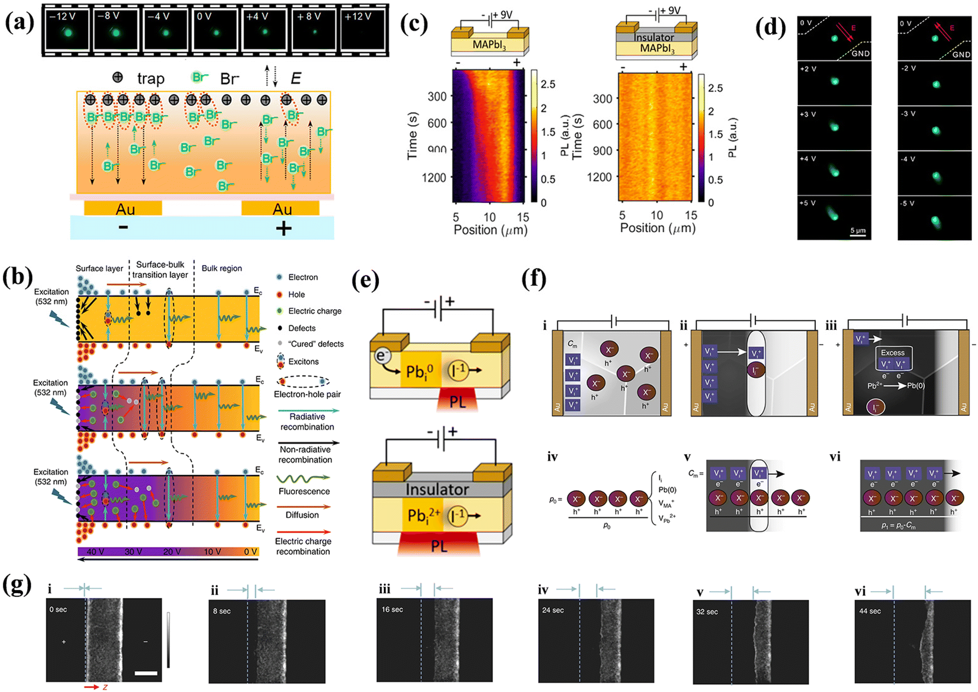 | ||
| Fig. 8 (a) PL images of the MIS structure with voltages varying from −12 V to +12 V (top); schematic illustration of the electric-field-induced interaction between Br vacancies and excessive Br− (bottom). Reproduced with permission from ref. 3. Copyright 2021 American Chemical Society. (b) Schematic diagram of the three-step carrier transfer model for MPB SCBK with 532 nm excitation under no bias, appropriate bias, and excessive bias. Reproduced with permission from ref. 122. Copyright 2020 Springer Nature. (c) PL scan of a single line within the electrode gap for MAPbI3/Au (left) and MAPbI3/PMMA/SiO2/Au (right) during a bias of +9 V applied to the right electrode. Reproduced with permission from ref. 21. Copyright 2018 American Chemical Society. (d) Real-color PL images of a typical CsPbBr3 nanoplate device with different positive (left panel) and negative (right panel) bias voltages applied at the upper electrode. Reproduced with permission from ref. 124. Copyright 2018 American Chemical Society. (e) Schematic illustration of the redox processes of Pbi2+ in different MAPbI3 device structures. Reproduced with permission from ref. 21. Copyright 2018 American Chemical Society. (f) Interpretation of the dominant ionic effects. Diagrams proposing processes occurring during the application of an electrical field in the lateral electrode configuration. (g) Time-dependent PL images of a perovskite film CH3NH3PbI3−xClx under an external EF (∼2 × 10⁴ V m−1). The “+” and “−” signs indicate the polarity of the electrodes. (f and g) Reproduced with permission from ref. 118. Copyright 2018 Springer Nature. | ||
In the context of an applied EF, in addition to the response of charged defects, there is an additional case of carrier injection, which complicates the interaction process between the defects and carriers. Xing et al. delineated a universal three-step carrier transfer model, as illustrated in Fig. 8b.122 Owing to the commonly used preparation methods, numerous defects are generated both on the surface and within the bulk of the film. The three steps predominantly occur at the surface, surface–bulk transition layer, and bulk region of the material. In the absence of an EF, the photogenerated electrons and holes initially interact with the surface defects upon laser excitation. Subsequently, the remaining electrons and holes drift into the surface–bulk transition layer, where some are captured by the bulk defects. Upon diffusion into the bulk region, these carriers transition into free carriers, leading to a long-lifetime radiative recombination. The introduction of an appropriate EF increases the complexity by inducing both photogenerated and electrically injected carriers. Under the influence of EF, bulk defects gravitate toward the surface, while these surface defects capture some of the injected carriers, resulting in passivation. Furthermore, bulk defects can be healed by drifting photogenerated or injected carriers, thereby neutralizing the treated defects and increasing radiative recombination at the surface and surface–bulk layers. Moreover, excessive voltage introduces additional charge carriers that can mitigate pre-existing defects and generate new ones by capturing holes, thereby reducing the probability of radiative recombination. Hence, numerous studies have corroborated the potential for voltage regulation engineering to passivate surface defects and mitigate carrier-related issues.3,123
It is vital to understand the impact of the behaviors between injected carriers and defect on recombination mechanisms. Birkhold et al. studied PL quenching in MAPbI3 using lateral devices equipped with both charge-injecting and insulator-coated blocking contacts.21 They witnessed PL quenching exclusively at injecting contacts when bias was introduced, whereas the MAPbI3 film displayed no defect-assisted charged ion migration without charge injection, as illuminated in Fig. 8c. Hu et al. showed that charged carrier transport is a vital process in defining the performance of CsPbBr3 nanoplates under an EF. Fig. 8d shows that when a lateral positive bias is applied, the emission spot adopts an elongated shape directed towards the top electrode, counter to the applied EF.124 The degree of elongation is directly proportional to the applied bias magnitude. Notably, under a negative bias, the emission spot extends towards the opposite electrode, always in a direction opposite to the applied EF. This elongation of the PL tail is attributable to the drift of photogenerated minority carriers under the applied bias. Importantly, the PL images exhibits less pronounced elongation at low temperatures, further substantiating the nuanced role of injected carriers in the presence of an EF.
Investigating the effects of vertical EF on defect behaviors is complicated because of the absence of more intuitive characteristics. Leijtens et al. fabricated MAPbI3−xClx capacitors using non-injecting Al2O3 contacts to examine the dynamics of defect-induced excited states at room temperature (RT) and 190 K, employing both PL and TrPL analyses to eliminate the effect of injected carriers.20 The field-induced PL was attenuated at RT, with distinct trends observed for the single- and double-molecular decays of PL. This attenuation arose from photoexcited carriers and charged defects drifting in opposite directions under EF, reducing the probability of radiative recombination while accumulating charged defects at the non-injecting interface. Conversely, at 190 K, the enhancement in the field-induced PL persisted even after the field was deactivated. This enhancement was attributed to the EF-induced alignment of organic cations at low temperatures, which limits the vibrational freedom and local shielding of the lattice between the organic and inorganic ions. This leads to stronger electron–hole interactions, accompanied by slower rates of charge drift, charged ion migration, and carrier capture at these low temperatures. Hence, the rate of radiative recombination surpassed that of nonradiative recombination. Under the influence of EF, PL quenching occurred in conjunction with carrier separation and drift, leading to a reduction in the nonradiative relaxation rate. This observation indicates that mobile defects under EF also have a significant impact on the rate of nonradiative recombination.
To realize efficient and stable PeLEDs, a comprehensive understanding of the defect behavior and carrier interactions in halide perovskite materials under operational conditions is imperative. Such an analysis will provide valuable scientific insights and theoretical frameworks essential for enhancing the fundamental properties of these materials, thereby addressing the challenges previously outlined.
3.3 Induced new defects
When EF is applied to a device, defects are the first to respond to. However, the motion of one defect under the influence of EF can induce the formation of additional new defects, thereby altering the energy band structure. This process can result in vacancy–interstitial pairs, which complicates the differentiation between intrinsic and field-induced defects. Although the transformation of semiconductor electrical morphology induced by ions remains an area for further investigation, the mechanisms governing the generation of new defects in PeLEDs under EF is also a subject of active research. Theoretical and experimental studies have been conducted to propose various models to elucidate these phenomena.The proposed mechanism suggests that EF can promote the migration of various defect types, such as point defects, vacancies, and interstitials, leading to the formation of new defects, as discussed in Section 3.1. This defect migration can subsequently generate charge carriers and their recombination, leading to light emission. In standard device configurations, these defects often interact with the injected carriers. Birkhold et al. reported that injected electrons can interact with existing defects to form new nonradiative defect centers, specifically Pbi0, through the electrochemical reduction of Pbi2+.21 A diagram of the redox process is shown in Fig. 8e. DFT calculations indicate that Pbi2+ resides above the CBM with a defect energy level of 0.08 eV, whereas Pbi0 forms a deep trap state at 0.47 eV below the CBM, corroborating observed PL bursts in Fig. 8c. However, such phenomena are absent in devices without electron injection. Bisquert et al. extended this understanding by exploring the role of interstitial Pb(0),118 and employed p-type doped MAPbI3 with defect types including Ii, VMA, VPb, and lattice Pb(0) for their investigation. Among the inherent defects studied, only Ii can form deep energy levels while being neutralized by VI, thus mitigating the quenching centers. Furthermore, excess VI can trigger redox reactions that convert the interstitial Pb2+ to Pb(0), as illustrated in Fig. 8f. Both Ii and Pb(0) serve as nonradiative recombination centers that quench the PL images, as shown in Fig. 8g. Huang et al. also reported that ferroelectric polarization in perovskite polycrystalline films could induce grain polarization and ion migration, creating new defects when the polarization strength surpasses 1.0 V μm−1.84 Using Br/Cl mixed-halide NCs as a research object, Liao et al. investigated the defect behavior in PeLEDs with varying numbers of layers of NCs under EF.125 They pointed out that multilayered NC devices, which undergo drift of Cl− between adjoining NCs under the action of the EF, induce a new defect region with Cl-deficient, which leads to spectral instability and degradation of the device. In contrast, devices with single-layered NCs can efficiently curb the process. However, the excess holes injected, coupled with the electrochemical reaction react with Cl−, lead to the generation of irreversible chlorine vacancy regions. Such defects constitute deep traps and nonradiative recombination centers.
An alternative mechanism imply that EF can induce the formation of new defects through electrostriction or piezoelectric effects. In this scenario, EF causes strain within the perovskite material, resulting in new defect formation and the consequent modulation of the electronic structure of the material. Supporting this notion, Wieghold et al. utilized SMA-STM to study the bandgap of Cs0.05(FA0.83MA0.17)0.95Pb(I0.83Br0.17)3.18 Their findings revealed a marginal reduction in the bandgap with increasing EF strength, with an even greater reduction observed under illumination. This behavior can be attributed to charged defects, which alter the crystal structure and in turn influence electron–phonon coupling, subsequently affecting the carrier recombination dynamics. DFT calculations further corroborate these observations, confirming changes in lattice constants, bandgap, and optical absorption characteristics with enhanced EFs.
Overall, the behavior of defects in PeLEDs under EF presents a complex and not yet fully understood landscape at the microscopic level. Currently, the majority of research in this area is focused on ion migration, with considerable efforts directed towards the development of passivation techniques to mitigate this phenomenon. Despite these efforts, advancements in microscale analysis of defect behavior have been relatively slow. Many studies have employed changes in the PL in the presence of a lateral EF to investigate the interactions between defects and both photogenerated and injected carriers. The application of an external EF in PeLEDs can lead to the segregation and translation of photogenerated carriers, affect the inherent defect migration, and generate new defects that alter the density of states, ultimately affecting both radiative and nonradiative recombination mechanisms. However, the situation under vertical field conditions remains relatively unexplored. Hence, a comprehensive understanding of carrier recombination dynamics, defect migration, and charge capture under EF modulation is pivotal for improving the performance of PeLEDs and accelerating their path to commercialization.
4. Management of defects
To overcome the hindrance caused by defects that adversely affect device performance under EF conditions, researchers worldwide are exploring a range of passivation strategies. Various similar but not identical procedures, such as ligand engineering, additive incorporation into precursor solutions, and inclusion of interfacial layers within devices, have been used to develop perovskite defect passivation. Considering high surface-area-to-volume ratio NCs, ligands can control nucleus growth and size regulation during synthesis, while post-treatment with ligands can fine-tune the surface chemistry of NCs, both allowing for comprehensive defect passivation from the inside out at the same time. Yet, incorporating a controlled ratio of additives into precursor solutions not only promotes the growth of high-quality crystalline films with fewer defects, but also elevates the PLQY and overall device efficiency. Importantly, device engineering remains crucial to unlock the full potential of near-perfect LHPs in achieving high-performance PeLEDs. The strategic insertion of compatible interfacial layers can further passivate defects in perovskite films and minimize the grain boundary issues. Therefore, this chapter provides a comprehensive overview of the latest advancements in each of these key areas.4.1 Defects passivation strategies in LHP NCs
![[thin space (1/6-em)]](https://www.rsc.org/images/entities/char_2009.gif) :1 molar ratio in a nonpolar solvent, as shown in eqn (15). The amino group of OLA can engage in coordinate bonding with unsaturated Pb2+ ions on the surface, utilizing its lone pair of electrons while in an unprotonated state.126 In contrast, computational studies suggest that R-NH3+ could occupy up to 50% of A-site cations on the surface in theory.127 Moreover, a portion of R-NH3+ passivates VBrvia hydrogen bonding, irrespective of the surface termination.128 The formation of ammonium carboxylate salts, as outlined in eqn (15), increases the dissolution of PbBr2, subsequently enhancing the production of Br− ions according to eqn (16). It is widely accepted that OLA forms robust bonds with NC surfaces. However, there is a debate regarding the role of OA in the surface bonding. Angshuman Nag et al. employed nuclear Overhauser effect spectroscopy (NOESY) to investigate whether OA exists as free ligands in the final colloidal dispersion, thus not binding to the NC surface.128 In post-purification solution, the addition of excess OLA enables OA to form alkylammonium oleate through ion pairs with amines, facilitating its enhanced surface adsorption,129 as illustrated in eqn (17). Brutchey et al. utilized 1H NMR and diffusion-ordered spectroscopy (DOSY) to suggest that both OA and OLA interact with the surface of NCs.130 In addition, their work contradicts the findings of De Roo et al., asserting that OA binds securely to the NC surface even without excess amines. Additional studies indicate that the R-COO− can coordinate with unsaturated Pb2+ and A-site cations through electron donation.56,126 Concurrently, long-chain OA may passivate surface X− to coordinate with Pb2+, thereby stabilizing the octahedral structure.131 In summary, it is generally acknowledged that due to the ionic nature of perovskite NCs, the formation of labile bonds between OLA/OA ligands and NC surfaces is inevitable.
:1 molar ratio in a nonpolar solvent, as shown in eqn (15). The amino group of OLA can engage in coordinate bonding with unsaturated Pb2+ ions on the surface, utilizing its lone pair of electrons while in an unprotonated state.126 In contrast, computational studies suggest that R-NH3+ could occupy up to 50% of A-site cations on the surface in theory.127 Moreover, a portion of R-NH3+ passivates VBrvia hydrogen bonding, irrespective of the surface termination.128 The formation of ammonium carboxylate salts, as outlined in eqn (15), increases the dissolution of PbBr2, subsequently enhancing the production of Br− ions according to eqn (16). It is widely accepted that OLA forms robust bonds with NC surfaces. However, there is a debate regarding the role of OA in the surface bonding. Angshuman Nag et al. employed nuclear Overhauser effect spectroscopy (NOESY) to investigate whether OA exists as free ligands in the final colloidal dispersion, thus not binding to the NC surface.128 In post-purification solution, the addition of excess OLA enables OA to form alkylammonium oleate through ion pairs with amines, facilitating its enhanced surface adsorption,129 as illustrated in eqn (17). Brutchey et al. utilized 1H NMR and diffusion-ordered spectroscopy (DOSY) to suggest that both OA and OLA interact with the surface of NCs.130 In addition, their work contradicts the findings of De Roo et al., asserting that OA binds securely to the NC surface even without excess amines. Additional studies indicate that the R-COO− can coordinate with unsaturated Pb2+ and A-site cations through electron donation.56,126 Concurrently, long-chain OA may passivate surface X− to coordinate with Pb2+, thereby stabilizing the octahedral structure.131 In summary, it is generally acknowledged that due to the ionic nature of perovskite NCs, the formation of labile bonds between OLA/OA ligands and NC surfaces is inevitable.| 2Cs-oleate + 3PbX2 = 2CsPbX3 NCs + Pb(oleate)2 | (14) |
| RNH2 + RCOOH ⇌ NH3+…COO− | (15) |
 | (16) |
| NH3+…COO− + RNH2 ⇌ (NH3+…RNH2)COO− | (17) |
The intricacy of surface chemistry of perovskite NCs is partly attributable to the interactions between various surface terminations and capping ligands. Bodnarchuk et al. proposed a likely model for the NC surface structure and discussed strategies for healing trap states on these surfaces, a key determinant of colloidal stability.132Fig. 9a delineates three potential surface terminations: [CsPbX3](PbX2){CsX}, [CsPbX3](CsX){PbX2}, and [CsPbX3](PbX2){AX′}. Here, [] donates the core, () represents the inner shell, and {} represents the outer shell, where A represents alkylammonium and Cs+, and X′ respond to halides and/or oleates. Among these, the {PbX2}-terminated model is highly improbable because of the necessity for a 2.5 times greater ligand packing density, resulting in steric hindrance and disruption of the octahedral coordination tendency of Pb2+. The most experimentally congruent model was [CsPbX3](PbX2){AX′}. Therefore, to achieve high-performance electrical and photophysical semiconductor properties directly influenced by the surface characteristics, it is essential to reconstruct the damaged (PbX2) surface and fortify the {AX′} outer layer to maintain the stability of the [PbX6]4− octahedra.
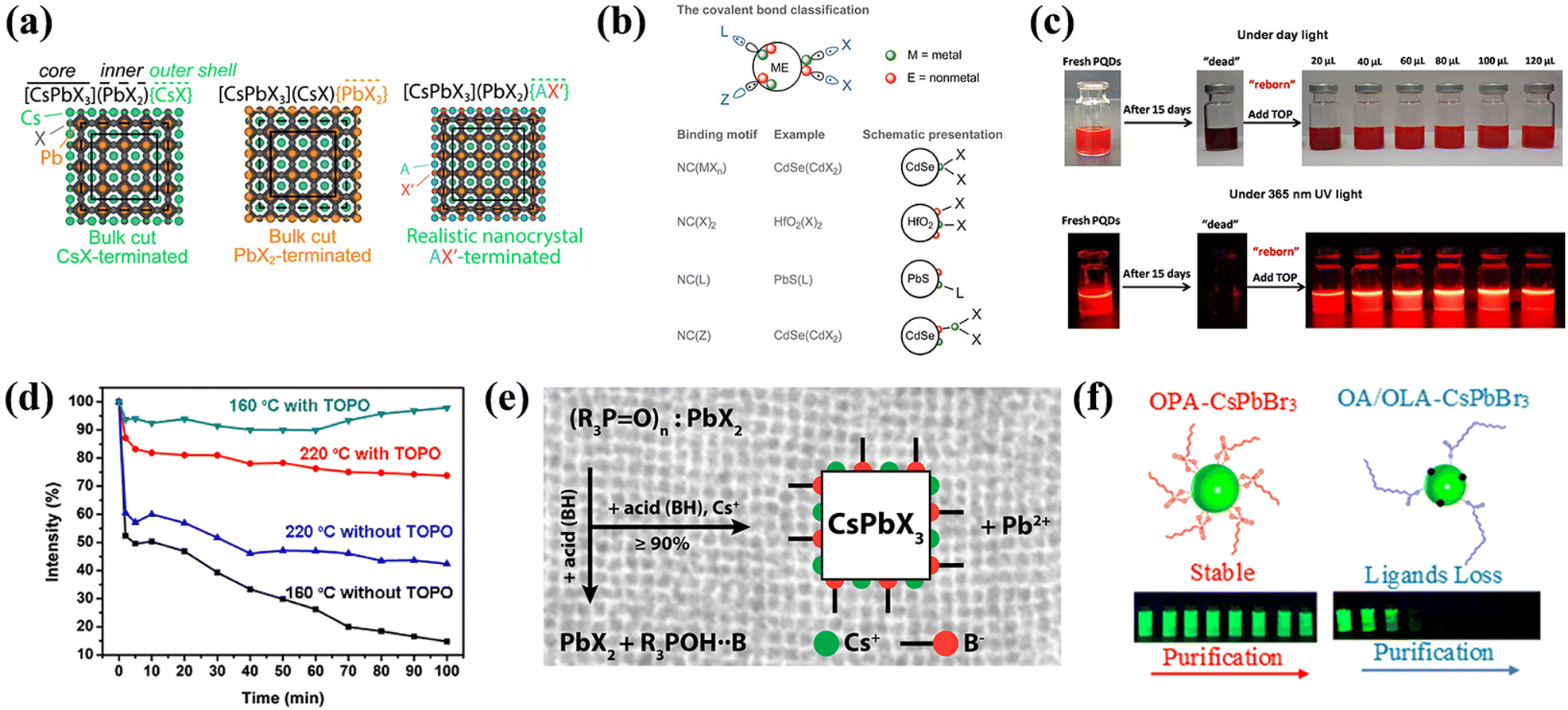 | ||
| Fig. 9 (a) The NC is arbitrarily divided into core, inner, and outer shell in three different ways. Reproduced with permission from ref. 132. Copyright 2019 American Chemical Society. (b) Schematic representation of the most important ligand classes within the covalent bond classification scheme. Reproduced with permission from ref. 129. Copyright 2016 American Chemical Society. (c) Photos of fresh/aged PNCs and aged PNCs with different amounts of TOP under daylight (top) and UV light (bottom). Reproduced with permission from ref. 135. Copyright 2018 American Chemical Society. (d) Intensity of PL emission as a function of CsPbBr3 NCs against ethanol treatment time. Reproduced with permission from ref. 143. Copyright 2017 American Chemical Society. (e) A schematic of how TOPO, PbBr2, acid, and Cs+ interact within the NCs synthetic system. Reproduced with permission from ref. 145. Copyright 2018 American Chemical Society. (f) Synthesis of CsPbBr3 NCs with OPA (left) and OA/OLA (right), schematic representation of the NC surface chemistry (top), and physical representation of the change in luminescence (365 nm excitation) after multiple purifications (bottom). Reproduced with permission from ref. 150. Copyright 2018 American Chemical Society. | ||
In summary, a thorough understanding of electro-optical performance of defect states and the surface chemistry of NCs is vital for achieving high-quality and stable LHP NCs. Existing challenges persist in the equilibrium between surface passivation and charge transport when traditional OA and OLA ligands are used. Recently, there has been an increase in research on novel ligands that not only bind more securely to the NC surface, but also exhibit outstanding transmission characteristics. Therefore, the subsequent section focuses on enhancing LHP NC passivation through ligand optimization. Further details can be found in Table 2.
| Perovskite | Ligands | Structure | Type (L, X, Z) | Classification | Ligands treatment methods | Material PLQYa/PLQYb (%) | EQEc/EQEd (%) | Ref. |
|---|---|---|---|---|---|---|---|---|
| a PLQY of the material before binding the new ligand. b PLQY of the material after binding the new ligand. c EQE of the device before binding the new ligand. d EQE of the device after binding the new ligand. | ||||||||
| CsPbI3 | Trioctylphosphine (TOP) |
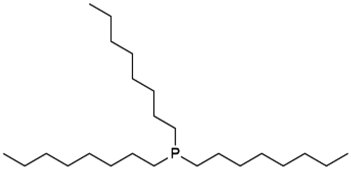
|
L | Phosphine acid | Post-treatment | 66/83 | —/— | 135 |
| CsPbBr3 | Trioctylphosphine oxide (TOPO) |

|
L | Phosphine acid | Used as synthetic ligands | 50/>80 | —/6.06% | 143 |
| CsPbBr3 | Octylphosphonic acid (OPA) |

|
L | Phosphine acid | Used as synthetic ligands | >80/>90 | 0.86/6.5 | 149 |
| CsPbI3 | Ammonium thiocyanate (NH4SCN) |

|
X | Thiocyanate | Used as synthetic ligands | 65/89 | 6.6/10.3 | 153 |
| CsPbBr3 | Sodium thiocyanate (NaSCN) |

|
X | Thiocyanate | Post-treatment | 92/99 | —/— | 154 |
| CsPbBrxCl3−x | Potassium thiocyanate (KSCN) |

|
X | Thiocyanate | Post-treatment | 34/74.1 | 0.6/2.04 | 156 |
| CsPbBr3 | Dodecanethiol (DDT) |

|
X | Thiocyanate | Post-treatment | 54/90–99 | —/— | 164 |
| CsPbI3 | 1-Octanethiol (OT) |

|
X | Thiols | Post-treatment | 76/88 | —/— | 168 |
| CsPbI3 | 1-Octadecanethiol (ODT) |

|
X | Thiols | Post-treatment | 52/93 | —/— | 171 |
| CsPbBr3 | Dodecylbenzene sulfonic acid (DBSA) |

|
X | Sulfonic acid | Used as synthetic ligands | —/>90 | —/— | 175 |
| CsPbI3 | Sodium dodecyl benzene sulfonate (SDSA) |
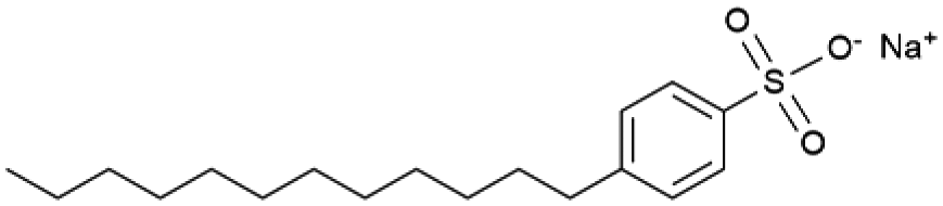
|
X | Sulfonic acid | Used as synthetic ligands | 42.2/90.7 | —/— | 176 |
| CsPbBrxCl3−x | Tetrabutylammonium p-toluenesulfonate (TBSA) |

|
X | Sulfonic acid | Post-treatment | 7/29 | —/2.6 | 177 |
| FAPbBr3 | 2-Naphthalenesulfonic acid (NSA) |

|
X | Sulfonic acid | Post-treatment | 46/93 | <15/19.2 | 178 |
| CsPbBr3 | 3-(N,N-Dimethyloctadecylammonio)propanesulfonate (SBE-18) |

|
X | Zwitterionic ligands | Used as synthetic ligands | >70/>90 | —/2.5 | 181 |
| CsPbBr3 | ZW–PIMA–PEG |

|
X | Zwitterionic ligands | Post-treatment | 55–60/70–80 | —/— | 185 |
| CsPbI3 | Lecithin |

|
X | Zwitterionic ligands | Used as synthetic ligands | 60/100 | 1.2/7.1 | 190 |
| MAPbI2Br | Ethylenediaminetetraacetic acid (EDTA) |

|
X | Zwitterionic ligands | Post-treatment | >50/>65 | 4.13/20.28 | 192 |
| MAPbBr3 | L-Cysteine |
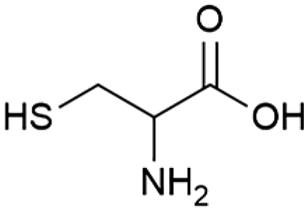
|
X | Zwitterionic ligands | Used as synthetic ligands | —/53.7 | —/— | 194 |
| MAPbBr3 | Succinic acid |
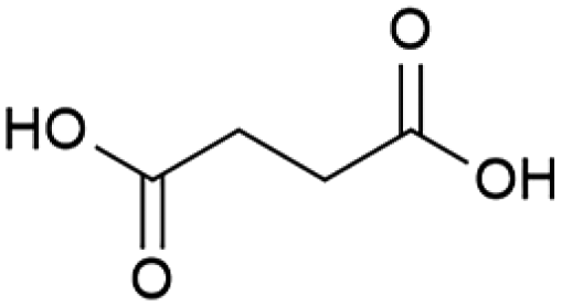
|
X | Zwitterionic ligands | Used as synthetic ligands | —/34 | —/— | 195 |
| CsPbI3 | 2,2′-Iminodibenzoic acid (IDA) |

|
X | Zwitterionic ligands | Post-treatment | 80 ± 5/95 ± 2 | 2.26/5.02 | 196 |
| CsPbBr3 | Oleylammonium iodide (OMA-I) |

|
X | Ammonium salts | Post-treatment | 38/80 | 0.17/21.3 | 197 |
| CsPbBr3 | Aniline hydroiodide (An-HI) |

|
X | Ammonium salts | Post-treatment | 38/69 | 0.17/14.1 | 197 |
| CsPbBr3 | Di-dodecyl dimethyl ammonium bromide (DDAB) |

|
X | Ammonium salts | Post-treatment | 49/71 | 0.1/3.0 | 198 |
| CsPbI3xBrx | Potassium oleate (K-OA) |

|
Z | Alkali metal salts | Used as synthetic ligands | 85/93 | 1.89/3.55 | 110 |
| CsPbI3 | Potassium iodide (KI) | K+ I− | Z | Alkali metal salts | Post-treatment | 75/96 | 16/23 | 200 |
L-type ligands.
Phosphine and phosphine acid. Phosphorus-containing materials interacting with the PNC particles during NC synthesis subsequently affect the colloidal stability of PNCs, with the effects varying based on the functional groups and carbon chain lengths attached to the phosphorus atom. Trioctylphosphine (TOP) has been successfully used to regenerate non-luminous aged CsPbBr1.2I1.8 NCs without detectable structural changes, as depicted in Fig. 9c,135 and to enhance the optical performance of fresh CsPbI3 NCs. Contrary to the prevalent view that TOP does not directly interact with the surface after treatment confirmed by X-ray Photoelectron Spectroscopy (XPS) and Fourier transform infrared spectroscopy (FTIR).135,136 TOP facilitates the release of R-COO− groups from their coordination with Pb2+ owing to the Lewis base effect, which is a critical factor in mitigating the degradation of α-CsPbI3 by further promoting chemical equilibrium.136 This mechanism results in effective surface passivation. However, Geyer et al. found that adding TOP to post-treatment CsPbI3 NCs considerably enhanced the phase stability of the solution.137 FTIR and XPS mapping data indicate that TOP acts as a capping ligand to protect NCs, albeit with a weak P peak, suggesting a limited quantity of P consistent with the fact that each TOP only has one P atom. This diverges from the conclusions of Zhang et al. Moreover, TOP serves as a coordinating alkylphosphine solvent to improve the reactivity of the PbI2 precursor forming TOP·PbI2 compound, thus accelerating nucleation and growth to yield high-quality CsPbI3 NCs.138 TOP is frequently used as an alternative to alkylammonium to improve the optical properties of LHP NCs in amine-free conditions. Xu et al. incorporated both TOP and lead stearate (Pb(St)2) in their synthesis approach to create an environment devoid of amines and acids.139 The dual carboxyl groups of Pb(St)2 were strategically utilized for robust surface passivation. One carboxylate facilitated the conversion of TOP to TOPO, whereas the other interacted with a Br− dangling bond, resulting in a Pb-rich surface with carboxylate-based passivation. In addition to TOP, phosphine-containing compounds such as triphenylphosphine (TPP),140,141 diphenylphosphine (DPP),142 and tributylphosphine, have also been widely explored, each showing varying degrees of enhancement in the performance of NCs.
Subsequent research has revealed the efficacy of the P![[double bond, length as m-dash]](https://www.rsc.org/images/entities/char_e001.gif) O functional group in improving both the crystallinity of NCs and efficiency of PeLEDs. The first ligand featuring a PO group applied to the perovskite NC system was trioctylphosphine oxide (TOPO), which was a branched capping ligand, conferring strong steric stability at high temperatures. Zhang et al. mixed TOPO and OA/OLA to synthesize TOPO-capped CsPbX3 NCs using a hot-injection method.143 In FTIR, the peak at 1155 cm−1 is attributed to C–P stretching, confirming that TOPO is anchored to the surface. TOPO increased the thermal stability threshold for obtaining monodisperse NCs to 260 °C and demonstrated exceptional resistance to degradation by protonic solvents, such as ethanol, as displayed in Fig. 9d. Kim et al. fabricated a PeLED structure (ITO/PEDOT:PSS/VB-FNPD/NCs/TPBi/LiF/Al) treated with a Zn-TOPO complex,144 achieving high EQE (7.12%, 6.06%, and 0.56%) and CE (9.93 cd A−1, 32.5 cd A−1, and 0.88 cd A−1) for red, green, and blue devices. TOPO possessing L-type ligand properties, readily forms complexes with Zn2+ from excess ZnX2 raw material, offering Zn-TOPO the properties of a Lewis acid to passivate halide defects. 31P NMR and XPS revealed that TOPO adheres to the surface of NCs only when coordinated with Zn2+, generating a reduction in Pb–O lattice bonding. Interestingly, when TOPO fully replaced OLA in a formulation that also included OA, it was largely absent from the ligand shell, which was exclusively passivated by Cs-oleate, a finding corroborated by Manna et al. in 2018.145 Solvent acidity and the degree of TOPO protonation were found to influence both the reactivity of the PbX2 precursor and the size distribution of the NCs, as shown in Fig. 9e. In addition to TOPO, ligands featuring PO groups, such as triphenylphosphine oxide (TPPO)146,147 and tris(4-fluorophenyl)phosphine oxide (TFPPO),148 have also been used to effectively passivate reduced-dimensional perovskites.
O functional group in improving both the crystallinity of NCs and efficiency of PeLEDs. The first ligand featuring a PO group applied to the perovskite NC system was trioctylphosphine oxide (TOPO), which was a branched capping ligand, conferring strong steric stability at high temperatures. Zhang et al. mixed TOPO and OA/OLA to synthesize TOPO-capped CsPbX3 NCs using a hot-injection method.143 In FTIR, the peak at 1155 cm−1 is attributed to C–P stretching, confirming that TOPO is anchored to the surface. TOPO increased the thermal stability threshold for obtaining monodisperse NCs to 260 °C and demonstrated exceptional resistance to degradation by protonic solvents, such as ethanol, as displayed in Fig. 9d. Kim et al. fabricated a PeLED structure (ITO/PEDOT:PSS/VB-FNPD/NCs/TPBi/LiF/Al) treated with a Zn-TOPO complex,144 achieving high EQE (7.12%, 6.06%, and 0.56%) and CE (9.93 cd A−1, 32.5 cd A−1, and 0.88 cd A−1) for red, green, and blue devices. TOPO possessing L-type ligand properties, readily forms complexes with Zn2+ from excess ZnX2 raw material, offering Zn-TOPO the properties of a Lewis acid to passivate halide defects. 31P NMR and XPS revealed that TOPO adheres to the surface of NCs only when coordinated with Zn2+, generating a reduction in Pb–O lattice bonding. Interestingly, when TOPO fully replaced OLA in a formulation that also included OA, it was largely absent from the ligand shell, which was exclusively passivated by Cs-oleate, a finding corroborated by Manna et al. in 2018.145 Solvent acidity and the degree of TOPO protonation were found to influence both the reactivity of the PbX2 precursor and the size distribution of the NCs, as shown in Fig. 9e. In addition to TOPO, ligands featuring PO groups, such as triphenylphosphine oxide (TPPO)146,147 and tris(4-fluorophenyl)phosphine oxide (TFPPO),148 have also been used to effectively passivate reduced-dimensional perovskites.
Alkylphosphonic acids, known for their dual chelating sites, offer robust affinities to NC surfaces and are frequently utilized as alternatives to OA and OLA.149 For instance, octylphosphonic acid (OPA) promotes the dissolution of precursors without requiring amines, due to its acid-dissociation properties. Moreover, OPA's dual chelation sites formed close associations with Pb2+, accelerating both nucleation and growth processes.150 This leads to the formation of highly stable NCs that are resistant to antisolvents, as illustrated in Fig. 9f. These characteristics have contributed to advancements in device fabrication. Compared with OA/OLA, OPA has shorter carbon chains (8C), which facilitates the removal of detrimental organic ligand residues from OPA–CsPbBr3, yielding highly planar films and devices with an EQE of 6.5%. Additionally, bis(2,2,4-trimethylpentyl)phosphinic acid (TMPPA) serves as an excellent alternative to OA in synthesizing CsPbI3, producing high-quality NCs that resist transitioning to the δ-CsPbI3 phase.151
X-type ligands.
Thiocyanate. Thiocyanates, considered pseudohalides, offer superior stability over halides and present a promising alternative for perovskite anions, thereby opening new avenues for the tailored design of optoelectronic properties in hybrid inorganic/organic perovskite materials.152 In contrast to the spherical geometry of X−, the SCN− feature a rod-shaped structure, allowing the lone pairs of electrons from both S and N atoms to engage in robust chemical interactions with NC surfaces.153 Previous research has noted the similarities in ionic radii and electronegativity between SCN− (217 pm) and I− (220 pm).152 Hence, it has been shown that the introduction of ammonium thiocyanate (NH4SCN) in the synthesis of CsPbI3 NCs can improve crystal quality without lattice incorporation, while reducing surface defects and grain boundaries.154 Specifically, the dangling Pb2+ bonds interact with SCN− to form Pb–S bonds, thus decreasing surface defects and the CBM of CsPbI3. This results in an improved electron injection efficiency and an increase in the EQE from 6.6% to 10.3%.
In earlier studies, the role of SCN− was shown to be significant in Br-based NCs. Alivisatos et al. reported that post-synthetic treatment of CsPbBr3 NCs with either NH4SCN or NaSCN powders effectively renovated the lead-rich surface, mitigating shallow electron traps without altering the shape or crystalline structure of the NCs.155 FTIR analyses pointed that Na+ or NH4+ ions engaged with oleate species, while SCN− ions interacted specifically with Pb2+. Although SCN− occupied only 10–15% of the surface sites, it ensured a monoexponential decay profile (Fig. 10a), nearly unity PLQY, and improved the colloidal stability of CsPbBr3 NCs. Similarly, Tian et al. combined NaSCN with DDAB to modulate bromine vacancy density, thereby passivating surface defects and enhancing the stability of NCs.156 The integration of this surface treatment into a solution-processed LED structure led to a significant enhance the maximum luminance from 550 to 1200 cd m−2 and a reduction in the turn-on voltage.
 | ||
| Fig. 10 (a) Time-resolved photoluminescence at room temperature for fresh CsPbBr3 before and after ammonium thiocyanate treatment. Inset figures highlight the differences in the untreated and treated samples at early decay times. Reproduced with permission from ref. 155. Copyright 2017 American Chemical Society. (b) Curves of ΦPL and photographs of sample under UV light (insight) over time for as-synthesized and DDT-treated CsPbBr3 NCs. Reproduced with permission from ref. 165. Copyright 2019 American Chemical Society. (c) Photoluminescence quantum yield (PLQY) of as-synthesized, aged (6 days), and DSH-treated CsPbI3 NCs instantly after treatment (DSH_Instant) and after 1 day (DSH_1Day). Reproduced with permission from ref. 168. Copyright 2023 Wiley-VCH. (d) Binding motif on CsPbBr3 NC surface and interaction strength of OLA, OA, and DBSA ligands. Reproduced with permission from ref. 176. Copyright 2019 Wiley-VCH. (e) Schematic illustration of the halogen exchange process triggered by TBAS and SDSA. Reproduced with permission from ref. 178. Copyright 2020 American Chemical Society. (f) Schematical diagram of the effect of the betaine-capped NCs. Reproduced with permission from ref. 185. Copyright 2023 Elsevier Ltd. | ||
In addition to Na+ and NH4+ ions, the cations of thiocyanates, KSCN157 and Pb(SCN)2,152,158 are widely used in LEDs. K+ seized X− and worked with SCN− to impede the halide migration through coordinated bonding with detrimental uncoordinated halide sites and vacancies, obtaining high EQE (2.04%) and stability of blue PeLED (∼470 nm) without halogen separation.157 Pb(SCN)2, usually employed as the lead source, can partially or completely substitute PbX2 without introducing impurities. Due to the ambidentate linear structure of SCN−, these ligands function as spacers between distinct NCs, hindering aggregation and improving colloidal stability.158 Notably, the chemical bond strengths of Pb–S or Pb–N surpass that of Pb–Br, enabling SCN− ions to distort the crystal structure and up-shift the CB position.152 Additionally, the organic pseudohalide n-dodecylammonium thiocyanate (DAT) has been deployed as a ligand in mixed halide (Br/Cl) perovskites as well.159 The SCN− ions sourced from DAT effectively filled Cl vacancies and removed electron traps within the bandgap. This optimization led to the production of high-efficiency blue PeLEDs with an emission wavelength of approximately 470 nm and EQE of 6.3%.
The incorporation of SCN− ions can modulate both the optical properties and carrier dynamics related to the radiative recombination processes in perovskite materials. For instance, NaSCN has been shown to completely suppress the formation of charged excitons that are detrimental to PLQY.160,161 Moreover, SCN− ions have been found to hide the flickering phenomenon162 and are widely utilized in solar cell applications.163
Thiols. As X-type ligands, alkanethiols of different chain lengths can form Pb–S bonds, significantly decreasing surface energy and maintaining the stability of perovskite materials.164 Dodecanethiol (DDT), with its 12C chain, acts as a suitable ligand for post-treatment in the CsPbX3 system, often in conjunction with OA/OLA.165–168 DDT undergoes a thiol–ene reaction with OA, OLA, and octadecene (ODE) to become a thioether, as shown in Fig. 10b. These thiol and/or thioether ligands exhibit strong binding affinity to uncoordinated Pb2+ ions, inhibiting Pb0 formation and achieving near-unity PLQY.165 However, Jeon et al. found that DDT treatment, while increasing PLQY, also reduced the material's lifetime due to the production of nonradiative VBr recombination fractions.166 Additionally, DDT plays a dual function in rejuvenating the degraded α-CsPbI3 NCs, as shown in Fig. 10c. Notably, α-CsPbI3 NCs are susceptible to environmental degradation and often transform into a non-luminous δ-phase through the “α–γ–δ” pathway. DDT serves two objectives when added to the “sicked” CsPbI3 NCs: (i) it binds with Pb2+ and I− ions to passivate existing “healthy” NCs and (ii) it utilizes its etching capabilities to promote the α-CsPbI3 phase by selectively removing the heavily aged Cs4PbI6 components.168 Consequently, significant improvements in both the PL and environmental stability were observed. Moreover, DDT in synergy with AlX3 can catalyze the morphological transition from nanocubes to nanoplates.167
The 1-octanethiol (OT), characterized by its relatively short aliphatic alkyl chains, facilitates robust surface adsorption due to minimal steric hindrance.169 Through comparing the different lengths of the aliphatic alkyl chains, the thiol functional groups in OT anchored to Pb2+, hindering the structural transformation and improving the photostability. Deng et al. reported enhanced stability through a multi-step ligand exchange process involving OT, which yielded a stable passivation molecular layer that withstood ethanol washing.164 Moreover, the in situ incorporation of OT as capping ligands during synthesis markedly improved the tolerance of high-temperature and high-humidity conditions.170 It has been found that 1,3-propanedithiol (PDT) and OLA together trigger irreversible transformation of CsPbBr3 to Cs4PbBr6. PDT serves as a capping ligand to regulate the size uniformity and chemical stability of Cs4PbBr6 NCs.171 In addition, materials containing –SH groups, such as 1-octadecanethiol,172 butanethiol,173 green fluorescence BODIPY molecule,174 and porphyrin-thiol,175 have been extensively studied for similar applications.
Sulfonic acid or sulfonates. Recently, ligands featuring sulfonate groups which are known for their strong acidity and electron-withdrawing capabilities, have garnered considerable attention. The sulfonate head of dodecylbenzene sulfonic acid (DBSA) interacts tightly with exposed lead ions, ameliorating electronic structural defects and repairing Br− vacancies. In Fig. 10d, the anchoring effect of sulfonate groups on the surface of CsPbBr3 NCs effectively minimizes exciton trapping and confers enhanced stability against degradation throughout purification, storage, and irradiation processes.176 Sodium dodecyl benzene sulfonate (SDSA)177 exhibits a notable affinity for CsPbI3 NCs due to –SO3− in the ligand strongly binding with uncoordinated Pb2+ and filling the VI. The inclusion of SDSA sustained a PL intensity of 83% after 60 days of environmental exposure. Furthermore, SDSA and tetrabutylammonium p-toluenesulfonate (TBSA) collectively facilitate halogen exchange between Cl− and Br− ions, enabling spectral tuning without requiring additional halogen compounds, as depicted in Fig. 10e.178 In comparison with dodecylbenzenesulfonic acid (DSA) and sodium p-toluenesulfonate (SSA), evidence suggests that both cationic and anionic components in TBSA and SDSA are essential for determining the direction and extent of the halogen exchange. The use of –SO3− for surface passivation increases the PLQY from 7% to 81%, with blue PeLEDs owning a promising EQE of 2.6%. The introduction of short-chain aromatic backbones like 2-naphthalenesulfonic acid (NSA) during the purification process not only substitutes for OA but also forms strong interactions with the NC surface through the sulfo group coordinate with Pb.179 The interaction between the NSA and FAPbBr3 NCs effectively doubled the PLQY from 46% to 93%, enhancing the surface performance. NSA–FAPbBr3 PeLEDs owned a three order of magnitude increase in current density and achieved a high brightness of 67
115 cd cm−2 with an exceptional EQE of 19.2%, which hindered efficiency roll-off. Moreover, molecules containing sulfonic acid groups have also showed potential as photosensitizers180 and as ligands for modulating nanoparticle size.181
Zwitterionic ligands. Recently, zwitterionic ligands have emerged as a novel class of capping ligands for PNCs, offering the advantage of simultaneous surface passivation by positively and negatively charged groups. The main difference between zwitterionic ligands and traditional ligands is including:182 (i) there is no potential for either mutual or external neutralization of cationic and anionic moieties via Brønsted acid–base equilibria; (ii) the surface of NCs is stabilized by a strong bidentate effect, establishing chemical equilibrium. As a result, improvements in the optical properties, colloidal stability, and charge transfer of PNCs have been observed. Specifically, the long-chain sulfobetaine zwitterionic molecule, such as 3-(N,N-dimethyloctadecylammonio)propanesulfonate (SBE-18) has been effectively introduced as a substitute for OA and OLA in CsPbBr3 colloidal systems, exhibiting enhanced durability even after four wash cycles due to its chelating ability.182 Despite its long alkyl chain, SBE-18 did not significantly impede charge transport, resulting in PeLEDs with an EQE of 2.5%. In contrast to the protonation and deprotonation processes observed in OA and OLA, SBE-18 uniquely anchor to the surface via amino and sulfonate groups, enabling simultaneous binding to both anions and cations.183 Experiments revealed that zwitterionic ligands-treated NCs surfaces often reduce the size uniformity of the as-synthesized colloid. However, the CsPbBr3 NCs coated with SEB-18 demonstrated homogeneity and yielded controllable average sizes, ranging from 3.5 to 16 nm.184 During solvent evaporation, SBE-18-treated NCs exhibited a propensity for long-range ordered superlattice formation. Similar effect in betaine-capped NCs contributed to high EQE values of 10.8% and enhanced durability, as shown in Fig. 10f.185
Zwitterionic polymers with enhanced solubility have garnered research interest. Traditional zwitterionic ligands often have limited solubility in nonpolar organic solvents because of their intrinsic dipole properties. By leveraging poly(isobutylene-alt-maleic anhydride) (PIMA) as the foundational structure and incorporating poly(ethylene glycol) (PEG) as solubilizing blocks, Mattoussi and colleagues synthesized polyzwitterionic polymers, denoted as ZW–PIMA–PEG, through nucleophilic addition reactions.186 These polymers feature both amine and sulfobetaine functional groups. The sulfobetaine groups in ZW–PIMA–PEG coordinated with Pb2+ ions, while the steric hindrance introduced by the short PEG segments enabled efficient surface passivation by facilitating close bonding to the surface. Utilizing this ligand enhanced the colloidal stability of the NCs, allowing their solubility in a broad range of polar solvents over extended durations (1.5 years) while concurrently preserving their photophysical attributes. Similar improvements in surface passivation and stability have been observed with poly(carboxybetaine acrylamide) (PCA)187 and poly(BMA-co-2-(methacryloyloxy)ethyl-sulfobetaine) (PBMA-SB).188 The strategic selection of functional groups allows for the design of photocrosslinkable zwitterionic ligands, thereby enabling the fabrication of directly patternable PNCs.189
The predominant functional groups in the amphoteric ligands include sulfobetaine, choline phosphate, and amino acids. Soy lecithin, a naturally abundant phospholipid, acts as an efficacious zwitterionic capping ligand that anchors robustly to its surface. The ligand density and spatial arrangement of lecithin chains contribute significantly to both solution phase formation and structural integrity across a wide concentration range, extending to as low as a few ng mL−1.190 Similarly, lecithin addition to CsPbI3 NCs enabled phase stability in ambient air for six months.191 PeLEDs fabricated with lecithin-capped NCs showed an EL peak at 634 nm, satisfying Rec. 2020 red standards, with the Lmax of 1391 cd m−2 and the operational T50 of 33 min. This high performance is primarily attributed to the interaction with lecithin to alleviate lattice strain and demonstrate a heightened affinity for the CsPbI3 surface.
In the synthesis of CsPbBr3 NCs, Grisorio and co-authors incorporated an auxiliary bromine source, 8-bromooctanoic acid (BOA).192 This compound ionizes to release Br− ions, while the residual moiety undergoes an SN2 reaction with OLA to form a zwitterionic ligand. This features both dialkylammonium and carboxyl groups, exhibiting a zwitterionic nature. The NCs capped with this zwitterionic ligand shown reduced solubility in nonpolar solutions, allowed purification using hexene, and maintained stability for three months in dichloromethane (CH2Cl2). Upon UV irradiation, the CsPbBr3 NCs underwent halide exchange with CH2Cl2 as Cl− sources, leading to a spectral blue shift.
Multidentate ligands. In contrast to other ligands, multidentate ligands offer multiple coordinating groups on the NC surface, yielding more stable and enduring bonds with NCs. The distinction between zwitterionic ligands and multidentate ligands lies in the fact that zwitterionic ligands carry both positive and negative charged components, whereas multidentate ligands establish multiple coordination sites with the metal via several functional groups. For instance, in Fig. 11a, the combined treatment of MAPbI2Br NCs with ethylenediaminetetraacetic acid (EDTA) and reduced L-glutathione (GSH) effectively bound surface Pb2+ ions, mitigated surface defects, and suppressed halide migration.193 This led to a high-efficiency red LEDs with a peak emission at 620 nm and an EQE of 20.3%. DFT calculations confirmed that EDTA and GSH maximized the formation energy of iodide Frenkel defects at 0.18 eV, lowering the likelihood. The experimental results indicated that EDTA played a key role in enhancing the device efficiency, while GSH exhibited a stronger surface attachment compared to EDTA, thereby proving more stability. The concurrent presence of amino and carboxyl functional groups is indispensable in the synthesis of NCs. Unlike individual ligands, such as OA or OLA, which contain either amino or carboxyl groups, peptides offer both functionalities within a single molecular structure.194 This dual functionality effectively passivates Br− vacancies and Pb2+ sites on the NC surface. Peptides, when varied in chain length and concentration, can regulate the optical properties and dimensions of MAPbBr3 NCs. Specifically, L-cysteine serves as a representative trifunctional amino acid ligand, featuring three functional groups: –NH2, –COOH, and –SH.195 This multifunctionality results in a 6.9-fold enhancement in PLQY and yields a PL lifetime of 642 ns. In the synthesis of NCs, replacing OA with succinic acid and combining OLA as a synergistic ligand led to enhanced aqueous stability.196 This is attributed to the dual carboxylic acid groups in succinic acid, which chelate two exposed Pb sites on the NC surface, thereby significantly improving the stability against the aqueous environment. Post-treatment passivation using 2,2′-iminodibenzoic acid (IDA) stabilized the α-phase in CsPbI3 NC-based red LEDs, achieving a PLQY exceeding 95%.197 IDA showed superior surface attachment compared to OA, owing to its dual carboxylic groups that securely coordinate with Pb sites. Utilizing IDA-NCs resulted in PeLEDs with a notable EQE of 5.02% and Lmax of 748 cd m−2. This enhanced performance is attributed to the effective electronic coupling between the LUMO of IDA and the conduction band edge of CsPbI3 NCs, rather than the conductivity of IDA.
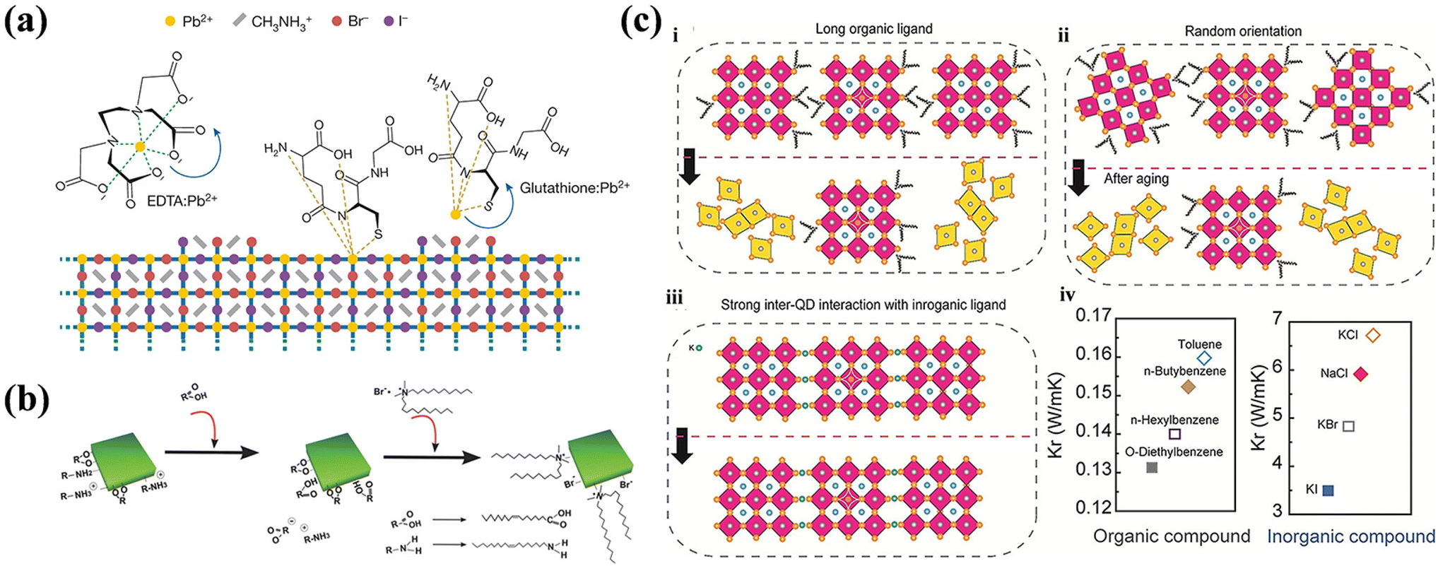 | ||
| Fig. 11 (a) Schematical diagram of the interactions of GSH and EDTA with Pb2+ atoms on the NCs surface. Reproduced with permission from ref. 193. Copyright 2021 Springer Nature. (b) The ligand-exchange mechanism on CsPbBr3 NC surfaces treated sequentially by OA and DDAB. Reproduced with permission from ref. 199. Copyright 2016 Wiley-VCH. (c) Formation of strained films with increased thermal transport. Reproduced with permission from ref. 201. Copyright 2021 Wiley-VCH. | ||
Ammonium salts. Ammonium salts are instrumental in optimizing the properties and applications of NCs through various means including surface modification, stability enhancement, optical property modulation, and biocompatibility. Ammonium compounds such as alkyl ammonium salts typically exhibit hydrophobic characteristics. They form adsorptive layers on NC surfaces, thereby enhancing both dispersibility and NC stability, and preventing aggregation and precipitation. Through the strategic selection of specific ammonium salts and modification of substituents, the surface properties of the NCs can be precisely tailored. This fine-tuning occurs because the positively charged moieties in the ammonium salts interact with the negatively charged regions on the NC surface, leading to effective defect passivation. For instance, Kido et al. conducted a comparative study on the anion-exchange effects of alkyl ammonium (oleylammonium iodide, OMA-I), and aryl ammonium salts (aniline hydroiodide, An-HI) as I− sources to deep-redshift emission.198 The addition of ammonium salts influenced not only the desorption of OA from the original NC surface, but also the surface ligand density. CsPbI3 PeLEDs treated with long alkyl-based OMA-I demonstrated a high EQE of 21.3% and superior color purity compared to aryl-based An-HI-capped NCs. However, devices with aryl-based An-HI-capped NCs demonstrated significantly higher operational stability, lasting 36 times longer. Additionally, the PLQYs of the colloidal solutions were 80% for OAM-I NCs and 69% for An-HI NCs, which was attributed to the effective suppression of anion defects. Bakr et al. utilized a halide ion pair-based capping agent DDAB to synthesize highly stable CsPbX3 NC films.199 This relatively compact ligand structure enhanced carrier mobility within the NC films and facilitated efficient PeLEDs fabrication. Effective DDAB passivation was achieved by incorporating OA into the synthetic solution. The acidic protons facilitated the protonation-mediated removal of the OLA ligands, resulting in the formation of acid–base complexes with deprotonated OA groups, as shown in Fig. 11b. These complexes promoted Br− coordination with Cs+ or Pb2+ ions and influenced adsorption onto the NC surface because of the steric hindrance of DDA+ while also maintaining the solubility of the NCs in toluene.
Z-type ligands.
Alkali metal salts. Z-type ligands are typically Lewis acids characterized by unoccupied orbitals that are capable of accepting electrons from surface atoms. In the octahedral [PbX6]4− structure, uncoordinated Pb2+ ions typically serve as Lewis acids, whereas the X− ions, acting as Lewis bases, commonly coordinate with them. At the present time, alkali metal salts provide empty orbitals to accept halogen atoms from the surface. The appeal of K+ ions stem from their small atomic radius and strong affinity for surface X− ions, generating significant interest in their interactions. Through the incorporation of potassium oleate (K-OA) during the synthesis of CsPbI3−xBrx NCs, we have highly achieved color-stable pure red PeLEDs and PL stable NCs for weeks, effectively mitigating halide migration phenomena.109 Synchrotron radiation photoemission spectroscopy (SRPES) characterization confirmed that the majority of K+ ions predominantly reside on the surface, facilitating robust interactions with Br− ions, weakening the bond between Pb2+ and Br−. A smaller fraction of K+ ions were situated within the interstitial spaces of the NCs. This dual effect of KBr termination efficiently passivates the surface defects, resulting in NCs with a remarkable PLQY exceeding 90%. Subsequent device fabrication demonstrated a significantly elevated EQE of 3.55% and luminance of 2671 cd m−2 compared to the control devices. Similar enhancement effects were also observed in blue CsPb(Br/Cl)3 NCs and devices, leading to the production of a spectrally stable and highly efficient blue PeLED, achieving a maximum EQE of 1.96% at the emission peak of 477 nm.200 Inorganic ligands maximize thermal conductivity compared to traditional organic ligands. Therefore, the incorporation of highly thermally conductive KI into the CsPbI3 system not only improved heat dissipation of the film but also promoted stronger interactions between dots, leading to stress relaxation and effective passivation of surface halide defects.201 The films of CsPbI3 NCs treated with KI exchange exhibited a close-packed and oriented arrangement, as depicted in Fig. 11c. Moreover, K+ ions were not doped into the lattice, facilitated mechanical coupling and exchanged surface OA and OLA desorption. The presence of K+ ions and all-inorganic ligands proved advantageous for enhancing device performance. The red LEDs demonstrated an impressive maximum EQE of 23% and an operating half-lifetime of 10 h, showing a notable 6% improvement compared to the control devices.
4.2 Passivation strategies for LHP films
The fabrication of polycrystalline perovskite thin films, whether via one- or two-step spin-coating methods, exhibits subtle distinctions compared to NCs. Notably, the latter approach yielded a higher grain boundary density. These grain boundaries contribute to elevated surface defect concentrations, subsequently influencing charge carrier transport and photoluminescence efficiency. Improvements in the performance of polycrystalline film devices can be achieved through various pre-processing techniques, including optimization of precursor solution concentration and ratio, solvent engineering, incorporation of additives, and the implementation of diverse post-processing strategies. Various post-processing strategies, such as annealing treatment and interface passivation, have been developed to passivate film defects. Pre-processing methods principally focus on controlling the nucleation rate and crystallization kinetics of perovskite films to attain well-defined crystal structures, thereby mitigating defect formation. In contrast, post-processing procedures are directed at reducing defects on the surface of perovskite thin films, thus enhancing their transport properties and ultimately leading to the realization of high-efficiency PeLEDs.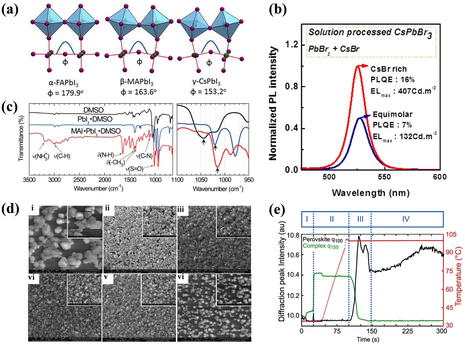 | ||
| Fig. 12 (a) Structural deformations of the ideal 180° B–X–B bond angle induced by the A-site cation size. Reproduced with permission from ref. 202. Copyright 2015 American Chemical Society. (b) Performance of PeLEDs based on CsPbBr3 films with and without excess CsBr. Reproduced with permission from ref. 205. Copyright 2015 American Chemical Society. (c) FTIR spectra of DMSO (solution), PbI2·DMSO (powder), MAI·PbI2·DMSO (powder), and expanded the fingerprint region for the SO vibrations. Reproduced with permission from ref. 216. Copyright 2015 American Chemical Society. (d) Top-view SEM images of MAPbBr3 films deposited on PEDOT:PSS/ITO substrates. The MAPbBr3 films were fabricated using solutions with different CB/DMF ratios of 0/1 (i), 1/10 (ii), 2/10 (iii), 3/10 (iv), 4/10 (v), and 4/10 (vi), respectively. Reproduced with permission from ref. 219. Copyright 2009 Royal Society of Chemistry. (e) Temporal evolution of radially integrated GIWAXS data of MAPI (black) and MAPI·DMSO solvent-complex (green) as well as temperature (red) during the crystallization process of perovskite solvent complex at 100 °C. Reproduced with permission from ref. 227. Copyright 2021, Springer Nature. | ||
Substituting the smaller MA+ cation with the larger FA+ cation led to a tolerance factor nearing 1, which expanded the octahedral structure slightly, resulting in enhanced luminance and repeatability in FAPbBr3 PeLEDs.203 Additionally, the incorporation of MA+ cations with high dipole facilitated the stabilization of the α-phase of FAPbI3 without necessitating high annealing temperatures.204 It is widely recognized that all-inorganic LHPs generally exhibit greater structural stability compared to hybrid organic–inorganic LHPs, primarily due to the chemical instability of MA+ or FA+ and asymmetry and instability of the coordination environment within the lattice structure.205 Inorganic cations like Cs+, which are more size-compatible with halides, can facilitate a more symmetric and stable coordination environment, thereby enhancing the overall stability of the perovskites. For instance, CsPbX3 perovskites demonstrate significantly elevated thermal decomposition temperatures (approximately 580 °C for CsPbBr3) compared to MAPbBr3 (approximately 220 °C).206 However, due to the relatively weak interaction between FA+ cations and halides, the introduction of Cs+ cations can effectively enhance crystallinity and improve optical/thermal stability.207 Similarly, when Cs+ is incorporated into MA-based perovskite crystals, thin films exhibit nearly complete surface coverage and display favorable emission characteristics.208 Conversely, the addition of MA+ molecules to all-inorganic CsPbBr3 films facilitate in reducing pinholes by controlling crystallization kinetics. This synergistic approach, combined with interface engineering, has yielded high-performance mixed-cation Cs0.87MA0.13PbBr3 PeLEDs with a peak brightness of 91000 cd m−2 and a peak EQE of 10.43%.209 In cases where an oversized A-site cation is used, it can lead to the segmentation of the 3D perovskite structure into multilayered quasi-2D perovskites with low defect generation, such as PEA2(CsPbBr3)2PbBr4.210 For example, through DFT calculations, the intercalation of aliphatic or aromatic alkylammonium cations between perovskite layers resulted in significant van der Waals interactions, as observed quantitatively. This increase in formation energy contributed to enhanced stability.211
In addition to A-site cation adjustments, the precise control of reactant stoichiometry plays a pivotal role in defect passivation. Reaction stoichiometry governs the exact correlation between substances involved in chemical reactions.56 In the context of perovskite precursor solvents, the standard chemical stoichiometric ratio of raw materials is 1:1, inevitably leading to the formation of defects, such as metallic lead atoms. Therefore, increasing the nonstoichiometric ratio of the raw materials has proven to be an effective strategy for reducing defect formation. Varying the concentrations of CsBr and PbBr2 in DMSO was found to decrease the defect density, resulting in enhanced performance of PeLEDs.205 This enhancement is evident in the prolonged PL lifetime and higher PLQY, as depicted in Fig. 12b. Employing a CsBr-rich solution led to an exceptionally narrow FWHM, increased luminescence, along with a decreased Von in PeLEDs. The incomplete reaction between MABr and PbBr2 at a 1:1 stoichiometry can lead to the formation of metallic Pb atoms.212 To avoid the generation of metallic lead atoms, incremental increases in the molar ratio of MABr by 2 to 7% in the MAPbBr3 solution were successfully accomplished.213
In contrast to the demands of PSC applications, the control of A-site cations and nonstoichiometric ratios in perovskite materials involves not only the modulation of film morphology, but also the imperative reduction of grain size. This reduction is essential for facilitating efficient electron and hole confinement, enabling effective radiative recombination in LED devices. However, small grain sizes often lead to an increased prevalence of grain boundaries and defects. Therefore, the effective passivation of defects is a critical factor in upgrading LED performance. Achieving an optimal balance between promoting grain growth and effectively passivating defects is instrumental in fine-tuning the mixture of A-site cations and stoichiometric ratios.
Within the precursor solution system, Pb2+ acts as a Lewis acid, adeptly accepting electron pairs from X− ions or solvents such as N,N-dimethylformamide (DMF), dimethyl sulfoxide (DMSO), N-methyl-2-pyrrolidone (NMP), and thiourea, all of which serve as Lewis bases.56 This dynamic interplay establishes a nuanced acid–base equilibrium, fostering intricate interactions among these components to form an intermediate phase.7 This intermediate entity is crucial for affecting both the nucleation and growth processes of perovskites, subsequently exerting a specific impact on film morphology and defect density. As an illustrative example, we consider the formation of MAPbI3 perovskite films to elucidate the role of the solution in constructing the intermediate phase. Initially, PbI2 dissolved in a solvent exhibited a layered structure held together by van der Waals interactions. Upon the addition of MAI, competition arose between the solvent and the I− ions to coordinate with PbI2. On the one hand, a relatively low activation energy facilitated intercalation reactions between the layered PbI2 and I−. This process involves the dissociation and reformation of chemical bonds between Pb and I in PbI2, resulting in a series of iodoplumbate coordination complexes, including PbI3− and PbI42−. Notably, a discernible relationship emerged between the concentration of PbI42− and the density of charge recombination centers in the generated perovskite thin films.214 On the other hand, a highly coordinating solvent could displace I− ions from their coordination sites with Pb2+ ions by solvent molecules. Consequently, the presence of this intermediate phase within the precursor solution effectively hinders perovskite crystallization. However, it is essential to note that the current understanding of the formation of intermediate phases during perovskite crystallization is characterized by the absence of reliable experimental methods to directly confirm their presence.215 This challenge is primarily due to the rapid nature of the crystallization process and the inherent instability of these intermediate phases. Additionally, contentious debate remains regarding whether these intermediate phases manifest as distinct crystal lattice structures or amorphous phases. Summarily, dissolving PbI2 in DMF along with equimolar amounts of DMSO and MAI yielded intermediate phases of PbI2·DMSO and MAI·PbI2·DMSO, as corroborated by shifts in the stretching vibration of SO at 1020 cm−1 and 1015 cm−1, respectively, upon reaction with PbI2 and PbI2 + MAI, as depicted in Fig. 12c.216
From the preceding discourse, the influence of various solvents on the crystallization process and, consequently, the film morphology is a key consideration. These commonly used solvents, which subtly differ in polarity, solubility, and binding capabilities, produce diverse complexes during the precursor stage. Gutmann's donor number (DN) was employed to quantify solvent solubility of solutions in perovskite precursors, especially for cations and Lewis acids.217 Solvents with high-DN values tend to bind Pb2+ centers, suppressing the formation of iodoplumbate complexes and retarding perovskite crystallization. In contrast, solvents with low-DN values have weak Pb2+ affinity, enabling the formation of iodoplumbate complexes and supporting the growth of perovskite single crystals.218 By blending solvents with varying DN capabilities, it becomes possible to manipulate the shape of intermediate complexation species, adjust coordination interactions within the solution, and effectively control the crystallization process of perovskites.7 Wu and coworkers demonstrated a straightforward one-step solution-based approach for enhancing perovskite film morphology by utilizing a diverse range of DN values in a nonsolvent/solvent mixture. As depicted in Fig. 12d, the impact of different CB/DMF ratios on MAPbBr3 film morphology was evident, with an increase in the proportion of CB leading to enhanced coverage and decreased grain size.219 The improved film morphology was attributed to the influence of the combined solvent on the nucleation process during film formation, leading to an increased nucleation rate due to the low solubility of CB in the crystallization process. This led to a smaller grain size in the MAPbBr3 film. The achievement of high-coverage and small-sized films effectively reduced the device leakage current, resulting in a device with an Lmax of 3846 cd m−2.
Crystallization occurs upon reaching a state of supersaturation in the solvent, and the anti-solvent expedites this process by accelerating the nucleation rate of the perovskite film. This is achieved by adding the anti-solvent dropwise during the spin-coating process, which flushes away the solvent within the precursor, inducing supersaturation and rapid precipitation of the precursor solution.220 Increasing experimental evidence underscores the imperative role of incorporating anti-solvents as a specific method for producing uniformly dense films, while concurrently addressing inherent defects. The anti-solvent not only modulates the nucleation rate during spin-coating but also exerts a profound influence on crystal growth and film morphology. Commonly used anti-solvents in PeLEDs include CB, chloroform, ethyl acetate (EA), and mixed anti-solvent solutions. Comprehensive anti-solvent comparisons have revealed that CB, when employed as the anti-solvent, efficiently removes solvents from the precursor solution and leverages the inherent chloride ions within CB to adeptly passivate surface bromine vacancies in MAPbBr3, as substantiated by XPS analysis.221 Nonetheless, the high boiling point of CB at 132 °C presents a predicament as a substantial residue of CB often remains within the films, potentially posing toxic or hazardous environmental issues.222 In contrast, the eco-friendly green solvent EA, known for its low boiling point and easy removal after thermal treatment, offers a favorable option for generating denser and more uniform thin films.223 It is important to note that iodine-based films treated with EA tend to increase grain size, while bromine-based films exhibit only marginal increases while concurrently diminishing grain boundaries, effectively passivating defects at the grain boundaries.224 Therefore, MAPbBr3 films treated with EA exhibit an improved crystalline structure, refined morphology, and diminished defect density, thereby in turn enhancing the operational efficiency of the associated PeLEDs. Additionally, the timing of anti-solvent dropping during the film formation process also impacts surface morphology.225,226
Precise control of solvent engineering is of paramount importance because of its direct influence on surface morphology and defect states, thereby providing a means to regulate nucleation and crystal growth processes. Furthermore, there is a pressing need to expand the repertoire of solvent systems to accommodate diverse needs, particularly those related to eco-friendly solvents.
Annealing exerts similar effects in both the one- and two-step methods. In the two-step method, an annealing treatment was employed to facilitate diffusion between the two layers of thin films, such as diffusion from the PbI2/DMF solution to the MAI/IPA solution. Mativenga et al. varied the resting time between these steps to enable solvent-controlled growth of MAPbI3 thin films, yielding films with fewer residues, pinholes, and defects.230 During the intermediate resting period, gradual solvent evaporation mitigated the rapid evaporation of solvents in the second step, effectively decelerating the entire crystallization process and resulting in devices with reduced defects and enhanced performance. Furthermore, the residual stress in the lattice exhibited a linear dependence on the annealing temperature, with higher temperatures resulting in increased stress levels in the film.231 Typically, films prepared using the two-step method exhibit greater residual stress than those prepared using the one-step method.
Annealing treatments have garnered attention for their capacity to rectify undesirable structural232 and are acknowledged for inducing beneficial morphological transformations.233 In a vacuum-deposition process, Luo et al. successfully engineered low-dimensional perovskite thin films of PEA2(Csn−1PbnBr3n+1) and subsequently improved the device performance with an impressive EQE of 6.5% through post-annealing treatment. Comprehensive analyses, including PL, space-charge-limited current (SCLC), and PLQY, coupled with kinetic assessments, indicate the effectiveness of the post-annealing approach. This led to a notable reduction in defect density, enhanced film morphology, a five-fold decrease in nonradiative recombination, mitigated the unfavorable contribution of the small n-phase to luminescence, and heightened the potential for radiative recombination.
The annealing parameters, including the number of annealing steps, duration, and temperature, exert a substantial influence on both the formation of defect states within the film and the optical performance of the devices. Furthermore, the annealing process also impacts the construction of the intermediate phase between solvents and precursors, with both annealing time and temperature playing pivotal roles in this regard.234 On occasion, annealing can facilitate the transition between distinct perovskite phases; for instance, at 583 K, it induces the transformation from CsPb2Br5 to CsPbBr3.235 While solvent-vapor annealing is a well-established method, it finds greater application in PSCs236 and is less commonly employed in LEDs. This discrepancy primarily arises from the propensity for a liquid or quasi-liquid phase to form on the film's surface under vapor conditions, resulting in the recrystallization of atoms in regions where grains are less compact or not in contact, ultimately leading to the formation of larger grains.237 It is important to note that larger grains are generally unsuitable for light emission purposes.
Annealing, achieved through precise temperature control, is a valuable tool for optimizing microstructures within the crystal lattice and material interfaces. This enhances the intrinsic crystal quality and promotes the lattice homogeneity. Nevertheless, the selection of annealing conditions and their influence on the performance warrants further investigation. Careful consideration remains essential for determining the applicability of the annealing parameters in different application scenarios.
Organic additives. Certain organic molecules exhibit Lewis base characteristics, possessing available lone electron pairs that can interact with Pb2+, reduce halide vacancies, enhance optical properties, and improve the efficiency and stability of PeLEDs. One approach involves the use of nonionic dielectric Lewis base polyethylene glycol (PEG) in CsPbBr3 precursors, which physically fills grain boundaries and interacts with the perovskite crystal to passivate defect states.239 The interaction binding between Pb2+ and PEG effectively reduced nonradiative recombination, resulting in a one-order-of-magnitude decrease in the decay rate and a significant reduction in grain size. Furthermore, stoichiometric ratio adjustments through coordinated chemistry yielded luminance levels of 36
600 cd m−2 and an EQE of 5.34%. Other organic polymer additives with similar effects include poly(ethylene oxide),240 poly(2-ethyl-2-oxazoline),241 and polyhedral oligomeric silsesquioxane.242 Halide amines in ammonium salts can also passivate halide anions of the PbX64− octahedra through hydrogen bonding between the amino groups and three halogen anions, effectively reducing defects.56 For instance, multilayered quasi-2D perovskite films have been created by incorporating long-chain ammonium halides such as phenylethylammonium halides (PEAX),206n-butylammonium halides (BAX),243 and ethylammonium halides (EAX),210 transforming the dimension from 3D to 2D and facilitating bonding between the organic large cations and halides through hydrogen bonding. This approach is practical for producing pinhole-free films with low defect density. To prevent excessive crystal growth and alleviate surface defects, a substantial amount of bulky ammonium halide was introduced into quasi-2D perovskite films. However, akin to ligands in colloidal NCs, the excessive presence of ammonium halides can establish an insulating capping layer, hindering efficient carrier transport across nanometer-sized grains within the perovskite structure. Therefore, the inclusion of formamidine acetate (FAOAc) as an additive in CsPbBr3−xClx perovskite films led to the fabrication of highly efficient blue PeLEDs (∼477 nm).244 Acetate ions in FAOAc facilitated the removal of excess ammonium ions, while FA+ contributed to elevating the formation energy of the low-dimensional (n = 2) phase in Fig. 13a. This leads to the suppression of nonradiative recombination in the perovskite films, converting the n = 2 phase into a 3D phase. Consequently, efficient blue PeLEDs with a maximum EQE of 8.8% were achieved.
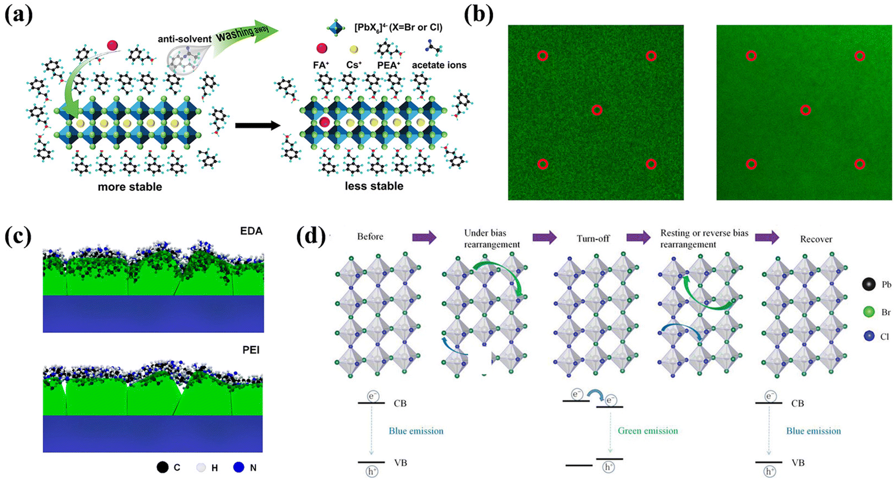 | ||
| Fig. 13 (a) Schematic diagram of quasi-2D perovskite with FAOAc addition. Reproduced with permission from ref. 244. Copyright 2021 Wiley-VCH. (b) Confocal microscopy images of perovskite film on NiOx (left) and NiOx/PVK (right) substrates. Reproduced with permission from ref. 257. Copyright 2019 AIP Publishing. (c) Schematic illustration of the depthwise penetration of PEI/EDA into MAPbBr3. Reproduced with permission from ref. 77. Copyright 2017 American Chemical Society. (d) Schematic diagram of halide ion migration under forward and reverse bias. Reproduced with permission from ref. 273. Copyright 2019 Wiley-VCH. | ||
Another approach is the introduction of additives into the anti-solvent and deposit them in a post-deposition treatment process, which reduces and mitigates nonradiative recombination defects in polycrystalline perovskite films. The organic small molecule ethoxylated trimethylolpropane triacrylate (ETPTA) functions as a functional additive that is incorporated into the anti-solvent.245 ETPTA effectively passivated and suppressed defects by interacting with undercoordinated Pb2+ ions through its CO group. This process relies on the ability of ETPTA in anti-solvent to cover the surface of the thin film and permeate the grain boundaries. The ETPTA passivation treatment resulted in a high EQE of 22.49% and a threefold increase in operational stability. Similarly, the addition of 9,9-spirobifluoren-2-yl-diphenylphosphine oxide (SPPO1), which contains phosphine oxide functionality, to the anti-solvent also facilitated the passivation of defects at grain boundaries, thereby enhancing device performance.246
Multifunctional molecules have proven effective not only in enhancing the performance of NCs but also in thin films. For instance, Xiao et al. synthesized a dual passivation additive, 4-fluorophenylmethylammoniumtrifluoroacetate (FPMATFA), which achieved dual passivation of both Pb2+ and X− in high-performance FA0.33Cs0.67Pb(I0.7Br0.3)3 red PeLEDs.247 FPMA+, with its strong NH3+ functional group at its end and electron-withdrawing F atom, enabled close binding with X− ions through hydrogen bonds. TFA− contributed lone electron pairs for interaction with uncoordinated Pb2+, as supported by XPS and DFT analyses. This intricate passivation strategy with FPMATFA led to a remarkable increase in EQE, reaching an impressive value of 20.9% in mixed-halide PeLEDs. Additionally, the harmful impacts stem from hysteresis and phase segregation, attributed to defects and ion migration, were significantly alleviated. Similarly, the bifunctional amino acid-derived additive 5-aminovaleric acid (Ava) also exhibited similar passivation effects.248,249
Inorganic additives. Currently, inorganic metal salts are the predominant choice for inorganic passivation, offering effective mitigation of X-site vacancy defects and grain boundaries in perovskite materials. For example, the systematic application of passivating potassium halide on both the surface and grain boundary regions has been demonstrated to reduce nonradiative losses and photoinduced ion migration within perovskite films and interfaces.250 Similarly, the use of lithium halides can yield analogous passivation effects, leading to devices with high EQE of up to 16.2%.251 Strategically dispersing metal ions within grain boundary crevices effectively passivates defects and raises the defect formation energy, thereby reducing defect occurrence.238 In addition to metal halide salts, certain inorganic salts containing thiolate ions can also serve as effective passivation agents for thin film defects. This is primarily because O atoms with unpaired electrons on the SO3− head group can form Lewis adducts, effectively coordinating with the Pb-exposed surface. Yang et al. effectively utilized methanesulfonate (MeS) in their study, and through rigorous analysis involving DFT calculations and NMR measurements, they demonstrated that MeS engaged in robust triple hydrogen bonding interactions with spacer BA cations.252 This interaction played a pivotal role in modulating the crystallization kinetics of the quasi-2D perovskite structure. The incorporation of MeS resulted in a weakened adsorbate blocking effect of BA, promoted the formation of Lewis adducts, and contributed to a reduction in uncoordinated Pb ions, ultimately alleviating defect formation within the perovskite films. These effects facilitate the transition from small-n to large-n phases, thereby enhancing radiative recombination in the higher n-phase. Consequently, the green LEDs employing these quasi-2D RP perovskite films achieved remarkable performance metrics, including a high CE of 63 cd A−1 and an exceptional EQE of 20.5%.
Lower interface passivation. The anode buffer layer, poly(3,4-ethylenedioxythiophene):poly(styrenesulfonate) (PEDOT:PSS), employed in PeLEDs, processes hygroscopic and acidic properties that can lead to detrimental etching of indium tin oxide (ITO) anodes.253 This etching effect results in exciton quenching and poses a substantial threat to the long-term stability of the devices. However, the relatively high injection barrier at the interface with perovskite hinders carrier injection. Indeed, commonly employed materials such as poly(9-vinylcarbazole) (PVK), poly(9,9-dioctylfluorene-co-N-(4-butylphenyl)diphenylamine) (TFB), and poly(N,N′-bis-4-butylphenyl-N,N′-bisphenyl)benzidine (poly-TPD) can function as interfaces between PEDOT:PSS and perovskite, effectively alleviating exciton quenching resulting from direct contact. These materials establish stepped energy level barriers, thus facilitating hole injection.254 Moreover, when an ultrathin LiF interlayer was applied to coat PEDOT:PSS, the wettability of the mixed DMF/DMSO solvent was enhanced. This enhancement is evident from the reduced contact angles observed on the coated surface compared to pristine PEDOT:PSS.255
Inorganic nickel oxide (NiOx) is a promising candidate for use as HTL in PeLEDs, owing to its highly favorable characteristics, including exceptional stability, high hole mobility, and effective electron-blocking ability.256–258 Nonetheless, the issue of nonradiative recombination leading to substantial PL quenching, primarily attributed to charge transfer events induced by defects occurring at the surface of the NiOx layer, has been a challenge. To avoid these quenching effects, an intermediate layer was strategically introduced between the NiOx and perovskite film. Sun et al. selected PVK as an intermediate layer, which significantly elevated the PLQY from 23% to 54%, resulting in an impressive EQE of 11.2% for a green PeLED.257 This notable enhancement is attributed to improved hole injection facilitated by the ladder energy band alignment of the NiOx/PVK layer and the suppression of nonradiative recombination processes, as depicted in Fig. 13b. The incorporation of this intermediate layer not only eliminates PL quenching but also enhances the crystallinity and overall stability of PeLEDs. Additionally, a synergistic approach involving the use of sodium dodecyl sulfate (SDS)-coated NiOx in combination with short oxygen plasma treatment has been successful in improving the crystallinity of the perovskite layer and facilitating hole injection efficiency.258 This strategy effectively suppressed quenching by leveraging the interaction between the CO group in SDS-OP and uncoordinated Pb2+, leading to efficient passivation of interfacial defects. The interfacial properties of SDS-OP contribute to the formation of a substantial surface dipole, a consequence of the combined effects of SDS layer dipoles and the increased concentration of Ni3+ species, ultimately resulting in an enhanced hole injection efficiency. Furthermore, a novel NiOx/LiF (1 nm)/perovskite interface has demonstrated superior wettability toward hydrophilic perovskite precursors and has successfully mitigated the effects of defect trap states on the NiOx surface.256
To enhance the perovskite film morphology and device stability, it is common practice to introduce ultrathin hydrophilic layers on poorly wetted bottom surfaces. You et al. employed this approach by depositing a hydrophilic insulating polyvinyl pyrrolidone (PVP) polymer interface layer on the ZnO ETL, leading to a vast reduction in perovskite film pinhole density.209 The improved wetting of the perovskite precursor solution on the PVP-modified substrate resulted in the uniform growth of perovskite films, thereby minimizing nonradiative recombination at the grain boundaries. Additionally, PVP passivated the surface defects in ZnO, reduced the electron-injection barrier, which, together with its insulating properties, ultimately improved the carrier balance. Similarly, inserting PMMA between the ZnO and MAPbBr3 interface effectively mitigated leakage current and minimized nonradiative recombination pathways.259 The ZnO substrate catalyzed an in situ amidation reaction with the dicarboxylic acids in the precursor, leading to the removal of organic components from the perovskite layer.260 These newly formed amides acted as interface barriers, preventing undesirable reactions between the perovskite layer and the underlying interface, ensuring stable contact at interface, and contributing to the overall stability of the devices (T50 = 682 h at 20 mA cm−2).
In PeLED devices, the extended diffusion length of LHP can lead to an imbalanced charge carrier transport, resulting in charge accumulation near the EML layer. In addition, the interface between the HTL and EML layers plays a crucial role in perovskite crystallization,261 emphasizing its significance. Various techniques similar to those employed for interface passivation are available to address the issues of the formation of defects. For instance, these techniques include introducing betaine as a passivating agent between the HTL and EML layers262 or using MAPbCl3 as an HTL layer to passivate defects at the interface.263 When designing the HTL/EML interface, considerations extend beyond defect reduction. Inserting nanostructures264 or Al2O3265 can also be considered to adjust the refractive index mismatch between the EML layer and substrate. This adjustment minimizes the photon losses in the waveguide and substrate modes, thereby maximizing the light outcoupling efficiency.
Upper interface passivation. Owing to the inherent structural softness of the perovskite lattice, the interactions between Pb2+ and X-site ions can be relatively weak, rendering the perovskite vulnerable to the formation of ionic surface defects during LHP deposition. Consequently, establishing an upper surface interface layer is an essential prerequisite for defect mitigation. This strategic insertion effectively neutralizes uncoordinated Pb atoms that contribute to nonradiative recombination centers while also reducing the presence of dangling bonds on the surface. Various amine-based passivating interlayers, including branched polyethylenimine (PEI) and EDA with different molecular sizes, were introduced to passivate defect sites in MAPbBr3 thin films, fabricating a highly efficient PeLEDs with excellent stability.77 This treatment addresses the defect sites by forming coordinated bonds between the nitrogen atoms from the amine-based molecules and the undercoordinated lead ions, leading to charge neutralization and a consequent decrease in the number of defect sites. Compared with PEI, a smaller EDA exhibited superior passivation effects on the top of film surface and penetrated deeper (Fig. 13c). Therefore, Song et al. gained outstanding PL intensity, no PL blinking, and enhanced device performance. A thin passivation layer of the organic small molecule TOPO was applied to coat the surface of quasi-two-dimensional perovskite thin films.266 PeLEDs utilizing PEA2(FAPbBr3)n−1PbBr4 (n = 3) exhibited green emission and achieved a remarkable CE of 62.4 cd A−1 and an EQE of 14.36%. This achievement primarily relies on the combination of TOPO and PbBr2 to passivate defects, effectively reducing nonradiative recombination at both the surface and grain boundaries. Similarly, the incorporation of a LiF interlayer on the EML/ETL surface served a dual purpose: it eradicated defects at perovskite grain boundaries and the surface by strengthening chemical bonds with uncoordinated Pb2+ ions, while also preventing perovskite emission quenching caused by the electron transport layer.267 Moreover, it reduces excessive electron injection, effectively maintaining carrier balance within the device.
4.3 Adjustment of drive modes
PeLEDs are typically driven by direct current (DC), which is a straightforward driving mode to realize effective luminescence. Nevertheless, DC driving comes into being continuous unidirectional current injection, resulting in unfavorable charge accumulation at the luminescent layers, especially at high current densities.268 This can compromise the device stability and induce adverse defect behaviors such as ion migration under EFs. In addition, DC driving requires power converters and rectifiers when connected to household alternating current (AC) power lines (110/220 V and 50/60 Hz), making inevitable power losses.269 Recently, there has been a growing interest in AC-driven EL devices, as they present a potential alternative mode to replace DC driving. AC driving involves the frequent reversal of the applied EF, effectively preventing charge accumulation and thermal degradation of devices, alleviating adverse defect behaviors and improving operational stability.270–272 The passivation methods discussed earlier, which address defects in NCs and thin films, are not only effective in reducing the defect impact under EF conditions, but also serve as universal defect passivation strategies applicable to devices in various scenarios. AC-driven devices leverage EFs to manage the defect behavior within perovskite materials. When subjected to an AC EF, defects at interfaces or within the EML become activated as charges.268 These charges, acting as hot electrons, tunnel into the EML to impact and excite emitting centers for light generation or form excitons with counter charges, ultimately in turn leading to light emission through recombination.268Under a DC bias, one detrimental defect behavior is ion migration, which can lead to spectral instability. However, AC driving mode effectively alleviated this issue. Tang et al. employed square-wave alternating voltage to drive devices and obtain stable ultra-pure CsPbBrxCl3−x blue PeLEDs (∼466 nm).273 Under DC operational bias, the mixed-halide perovskite film exhibited Cl-rich and Br-rich regions, resulting in spectral instability due to halide ion migration. This phenomenon was fully reversible upon resetting or applying a reverse bias (Fig. 13d). Utilizing reverse bias facilitates the rearrangement of halogen ions in mixed-halide devices. A square-wave alternating voltage was employed for 12 h to stabilize the EL spectra during the operation. Mobile ions accumulate at the surface of the perovskite emission layer induced by EF, which causes bond bending. This effect reduces the injection barriers for electrons and holes at forward and reverse voltages, enabling bidirectional AC EL. Hu et al. realized bidirectional AC EL using red quasi-2D PEA2MAn−1PbnI3n+1 films with different n-phase uniform distributions and symmetric device structures (ITO/PEDOT:PSS/PEI/PEA2MAn−1PbnI3n+1/P3HT/PEI/Ag).274 The distinct n-phase quasi-2D films provided varying optical bandgaps and energy levels of the conduction and valence bands to accept and transport injected carriers. Additionally, the accumulation of mobile ions at the film interface further reduces the energy barriers for carrier injection under AC voltage, enabling bidirectional electron–hole injection. This approach achieved a final EQE of 12.5% and EL irradiance of 24 W sr−1 m−2 at forward voltage and 3.7% and 18.3 W sr−1 m−2 at reverse voltage.
Under the influence of EF, both mobile defects and charge carriers exhibit response times to EF, which becomes more pronounced under AC EFs, especially with varying frequencies. In the context of the AC quasi-2D devices mentioned previously, the EL displayed a gradual response when subjected to a square-wave voltage, instantly disappearing when the voltage was removed (Fig. 14a). Moreover, at different frequencies (1/20/50/100 Hz), the response time lengthened with increasing frequency, indicating increased accumulation of mobile ions at the interfaces.274 Material properties also play a role in the response times. Fig. 14b illustrates that the EL response curves of MAPbBr3 and MAPbI3 under low-frequency and high-frequency AC sinusoidal voltage differ.275 Under low-frequency conditions, both the MAPbBr3 and MAPbI3 EL responses synchronize with the applied voltage crests. However, at high frequencies, a certain delay is observed because the transit time of the charge carriers exceeds the duration of a forward-bias half-cycle, requiring more time for recombination. The delay effect is more pronounced in MAPbBr3 because the recombination region is closer to the ETL under positive EFs, necessitating a longer receding time under reverse bias to retract the recombination region. Moreover, the ambipolar nature of the materials affects the reverse-bias EL intensity. For ambipolar materials such as MAPbI3, the reverse bias EL intensity is higher because the emission during the negative half-cycle primarily originates from residual charge carriers from the positive half-cycle.
 | ||
| Fig. 14 (a) EL profile of quasi-2D perovskite LEDs under forward (4.5 V) and reverse (−3.5 V) square-wave biases at different frequencies. Reproduced with permission from ref. 274. Copyright 2021 Elsevier Ltd. (b) EL and applied sinusoidal ac voltage as a function of phase angle for the LEDs based on MAPbI3 and MAPbBr3 at 75 Hz (top) or 5.6 kHz (bottom). Reproduced with permission from ref. 275. Copyright 2020 American Physical Society. (c) Normalized EL intensity of CsPbBr3 NCs LED as a function of voltage (left) and running time (right) under DC and AC driving conditions. Reproduced with permission from ref. 271. Copyright 2017 Wiley-VCH. (d) Integrated EL intensity versus Vpp (left) and excitation frequency (right) under different driving voltage modes (square wave and sine wave). Reproduced with permission from ref. 276. Copyright 2018 MDPI. | ||
Several efforts have been made to operate PeLEDs using AC voltage, with a focus on reducing the migration of ionic vacancies to enhance operational stability and increase EL intensity. Li and colleagues conducted a comparative study on CsPbI3 NCs under both DC and AC driving modes, observing alleviated efficiency roll-off and improved operational stability under AC mode (Fig. 14c).271 This effect primarily stemmed from the shorter operation time of AC driving compared with DC driving at an equivalent voltage, mitigating heat generation at high current densities. The frequent EF reversal also contributed to reducing charge accumulation in the defect states. Furthermore, they conducted a comparative analysis between sine and square pulsed bias to assess their effects on enhancing the device stability (Fig. 14d). It was observed that square pulsed bias yielded better EL intensity and operational stability due to the higher voltage magnitude of the square pulsed bias under the same peak-to-peak voltage (VPP).276 The EL intensity, whether driven by a sine or square pulsed bias, decreases with increasing frequency. This phenomenon can be attributed to the fact that the reverse voltage pumps out a larger number of injected carriers before they can recombine at higher frequencies. By employing a dual strategy of AC driving and ChCl interface passivation, it is possible to effectively passivate interface defects, suppress device heating, and reduce charge accumulation. As a result, stability is improved by a factor of four compared to DC driving.277
We recognize the inherent advantages of perovskite materials, including their high carrier mobility (ranging from 0.1 to 10 cm2 V−1 s−1) and long diffusion lengths (exceeding 500 nm). These properties enable low-frequency emissions when subjected to an AC EF and potential integration with household circuits. Moreover, in AC-OLEDs, the serial connection of multiple units capitalizes on the alternating nature of the AC voltage, facilitating the alternating emission of different colors during the positive and negative cycles. Implementing this approach in PeLEDs broadens the scope of the potential applications of these devices. When operated under a DC bias, thermal effects and the accumulation of defects at interfaces can result in device and material degradation. However, AC driving offers a solution to mitigate these issues, allowing for controlled management of defect behaviors.
5. Conclusion and future perspectives
In recent years, LHP materials have achieved remarkable advancements, which are emerging as promising candidates for next-generation display technologies. LHP materials exhibit notable advantages such as high EQE, cost-effective fabrication, exceptional color purity, and an extensive color gamut. Although research into the physics of LHP-based devices is currently experiencing rapid growth, there remains a substantial gap that must be bridged before commercial applications can be fully realized. LHPs are well known for their high tolerance to defects; however, recent investigations have indicated that defects play a pivotal role in constraining the attainment of high-performance PeLEDs. Therefore, our focus was on elucidating the behavior of defects and providing a comprehensive review of defect passivation methods.The formation of defects in PNCs and bulk films is influenced by a variety of internal and external factors. Among these factors, the study of defect behavior under EF is particularly pivotal, as an EF serves as an indispensable external operating condition for driving these devices. The behavior of defects in the presence of EF remains intricate and elusive. Under EF, defects undergo transformation into charged defects, leading to the movement of quasi-free charge carriers and ensuing ion migration. Ion migration, as a consequence of defect behavior, is particularly concerning for researchers due to its potential to cause device degradation and introduce color impurities. However, these adverse effects can be effectively mitigated through the application of targeted defect passivation techniques. A more profound understanding of the EF-induced defect dynamics behavior is still relatively limited. When devices inject or generate charge carriers or photocarriers under the influence of EF or illumination, the interaction between defects and carriers becomes notably intricate. Currently, PL variation serves as the primary tool for investigating the behavior of charge carriers and defects in the presence of lateral EF. Additionally, the movement of defects under an electric field can generate new, potentially harmful deep-level defects.
The challenge in achieving theoretical unity in understanding defect behaviors is partly due to the absence of direct visual characterization methods for defects. Although commonly used methods, such as microscopy, spectroscopy, and electrical measurements, have been reported in the literature, these methods primarily provide indirect responses to defect behaviors, which is not conducive to simple analysis. TOF-SIMS, a technique enabling the relative visualization of ion migration phenomena within devices, and a number of developed in situ characterization techniques provide valuable insights into how defect behaviors contribute to poor device performance.
Nowadays, extensive research is directed toward defect passivation with the aim of mitigating the adverse effects of defect behaviors and enhancing the performance of PeLEDs. In this review, we summarized the recent advancements in defect passivation within LHPs and examined them from three perspectives: NCs, bulk films, and driving methods. Defect passivation for NCs predominantly revolves around ligand control, which we have delineated with a focus on functional groups for optimizing both NC materials and devices. However, the choice of ligands for NCs creates problems of possible toxicity and stability, restricting their development. The commonly used encapsulation method increases the particle size, which is unfavorable for practical applications. Natural materials such as lecithin as a ligand are a potential material to expand the application of NCs in the biological field. Regarding the defect passivation methods for bulk films, we explored compositional adjustments, solvent engineering, annealing processes, additive engineering, and interface passivation. Current research has shown that using inorganic additives in bulk materials is cost-effective, suitable for mass production, and commercially viable. Furthermore, employing AC-EF that can be directly integrated with home circuits to drive PeLEDs presents a feasible approach and constitutes an important research target for future commercial applications.
Looking ahead, EF-induced LHP-based devices are ripe with opportunities and challenges. Research on EF-induced defect behavior primarily centers on the lateral EF, with limited exploration of vertical electric fields. In-depth research into the impact of vertical EFs on defect behavior is crucial, a topic that currently lacks consensus within the academic community. This highlights a significant research gap that demands to be addressed urgently and requires a concerted effort by researchers in their future work. This is not just vital for understanding the physics of the PeLEDs but also pivotal in eliminating the effects of ion migration, an essential step towards the early realization of commercial use.
Moreover, due to the toxicity concerns associated with lead in LHPs, there has been a growing focus on developing lead-free perovskites. Lead is highly water soluble and readily cycles through the food chain into the human body. Therefore, to safeguard public health, it is imperative for us to pursue the development of Pb-free PeLEDs vigorously, but the performance of current Pb-free devices still significantly lags far behind that of Pb-based perovskite because of self-trapped exciton emission and indirect bandgap. With vigorous development, non-toxic or low-toxicity Sn- or Ge-based PeLEDs are expected to improve performance gradually.
AC is emerging as a promising solution for mitigating the charge accumulation at interfaces induced by EFs. PeLEDs driven by AC can be directly connected to standard household circuits (110/220 V and 50/60 Hz) without additional power converters and rectifiers, reducing power loss. AC driving mode has the potential to achieve color-tunable emission, akin to OLEDs, under varying EF directions, fulfilling the desire for adjustable color displays. Therefore, AC driving is poised to become a significant research focus in the field of PeLEDs.
Author contributions
S. Z. and Z. X. conceived and designed the project. N. J. carried out research on the literature and drafted an initial version of the review. G. M. supported literature collection. All authors discussed the results and assisted during manuscript preparation.Conflicts of interest
The authors declare no conflict of interest.Acknowledgements
The authors express their thanks to the National Key Research and Development Program of China under grant no. 2021YFB3600403 and the National Natural Science Foundation of China under grant no. 62075006.References
- J. Wang, S. Wang, Y. Zhou, Y. Lou and Z. Wang, Sci. China Mater., 2022, 66, 1–21 CrossRef.
- Z. Ren, K. Wang, X. W. Sun and W. C. H. Choy, Adv. Funct. Mater., 2021, 31, 2100516 CrossRef CAS.
- Y. Gao, X. Li, W. Liu, X. Xing, H. Long, K. Wang, B. Wang and P. Lu, Nano Lett., 2021, 21, 10230–10237 CrossRef CAS PubMed.
- J. Lu, C. Yan, W. Feng, X. Guan, K. Lin and Z. Wei, EcoMat, 2021, 3, e12082 CrossRef CAS.
- X. K. Liu, W. Xu, S. Bai, Y. Jin, J. Wang, R. H. Friend and F. Gao, Nat. Mater., 2021, 20, 10–21 CrossRef CAS PubMed.
- H. He, S. Mei, Z. Wen, D. Yang, B. Yang, W. Zhang, F. Xie, G. Xing and R. Guo, Small, 2022, 18, e2103527 CrossRef PubMed.
- Y. Xia, Y. Lou, Y. Zhou, K. Wang, J. Chen, Z. Wang and L. Liao, J. Mater. Chem. C, 2022, 10, 3276–3286 RSC.
- L. Xu, S. Yuan, H. Zeng and J. Song, Mater. Today Nano, 2019, 6, 100036 CrossRef.
- Z. Tan, R. S. Moghaddam, M. L. Lai, P. Docampo, R. Higler, F. Deschler, M. Price, A. Sadhanala, L. M. Pazos, D. Credgington, F. Hanusch, T. Bein, H. J. Snaith and R. H. Friend, Nat. Nanotechnol., 2014, 9, 687–692 CrossRef CAS PubMed.
- K. Wang, Z. Y. Lin, Z. Zhang, L. Jin, K. Ma, A. H. Coffey, H. R. Atapattu, Y. Gao, J. Y. Park, Z. Wei, B. P. Finkenauer, C. Zhu, X. Meng, S. N. Chowdhury, Z. Chen, T. Terlier, T. H. Do, Y. Yao, K. R. Graham, A. Boltasseva, T. F. Guo, L. Huang, H. Gao, B. M. Savoie and L. Dou, Nat. Commun., 2023, 14, 397 CrossRef CAS PubMed.
- W. Bai, T. Xuan, H. Zhao, H. Dong, X. Cheng, L. Wang and R. J. Xie, Adv. Mater., 2023, 35, e2302283 CrossRef PubMed.
- W. Zhou, Y. Shen, L. X. Cao, Y. Lu, Y. Y. Tang, K. Zhang, H. Ren, F. M. Xie, Y. Q. Li and J. X. Tang, Adv. Funct. Mater., 2023, 33, 2301425 CrossRef CAS.
- J. Ye, M. M. Byranvand, C. O. Martinez, R. L. Z. Hoye, M. Saliba and L. Polavarapu, Angew. Chem., Int. Ed., 2021, 60, 21636–21660 CrossRef CAS PubMed.
- W. Tress, Adv. Energy Mater., 2017, 7, 1602358 CrossRef.
- M. Azam, K. Liu, Y. Sun, Z. Wang, G. Liang, S. Qu, P. Fan and Z. Wang, J. Phys. D: Appl. Phys., 2020, 53, 183002 CrossRef CAS.
- W. Li, M. U. Rothmann, Y. Zhu, W. Chen, C. Yang, Y. Yuan, Y. Y. Choo, X. Wen, Y. Cheng, U. Bach and J. Etheridge, Nat. Energy, 2021, 6, 624–632 CrossRef CAS.
- H. Kim, J. S. Kim, J. M. Heo, M. Pei, I. H. Park, Z. Liu, H. J. Yun, M. H. Park, S. H. Jeong, Y. H. Kim, J. W. Park, E. Oveisi, S. Nagane, A. Sadhanala, L. Zhang, J. J. Kweon, S. K. Lee, H. Yang, H. M. Jang, R. H. Friend, K. P. Loh, M. K. Nazeeruddin, N. G. Park and T. W. Lee, Nat. Commun., 2020, 11, 3378 CrossRef CAS PubMed.
- S. Wieghold, E. M. Cope, G. Moller, N. Shirato, B. Guzelturk, V. Rose and L. Nienhaus, ACS Energy Lett., 2022, 7, 2211–2218 CrossRef CAS.
- D. Ji, M. Na, S. Wang, H. Zhang, K. Zhu, C. Zhang and X. Li, Sci. Rep., 2018, 8, 12492 CrossRef PubMed.
- T. Leijtens, A. R. S. Kandada, G. E. Eperon, G. Grancini, V. D'Innocenzo, J. M. Ball, S. D. Stranks, H. J. Snaith and A. Petrozza, J. Am. Chem. Soc., 2015, 137, 15451–15459 CrossRef CAS PubMed.
- S. T. Birkhold, J. T. Precht, H. Liu, R. Giridharagopal, G. E. Eperon, L. Schmidt-Mende, X. Li and D. S. Ginger, ACS Energy Lett., 2018, 3, 1279–1286 CrossRef CAS.
- Y. Zhong, K. Liao, W. Du, J. Zhu, Q. Shang, F. Zhou, X. Wu, X. Sui, J. Shi, S. Yue, Q. Wang, Y. Zhang, Q. Zhang, X. Hu and X. Liu, ACS Nano, 2020, 14, 15605–15615 CrossRef CAS PubMed.
- M. A. Green, A. Ho-Baillie and H. J. Snaith, Nat. Photonics, 2014, 8, 506–514 CrossRef CAS.
- M. Ju, J. Dai, L. Ma and X. Zeng, J. Am. Chem. Soc., 2017, 139, 8038–8043 CrossRef CAS PubMed.
- C. Li, X. Lu, W. Ding, L. Feng, Y. Gao and Z. Guo, Acta Crystallogr., Sect. B: Struct. Sci., 2008, 64, 702–707 CrossRef CAS PubMed.
- C. J. Bartel, C. Sutton, B. R. Goldsmith, R. Ouyang, C. B. Musgrave, L. M. Ghiringhelli and M. Scheffler, Sci. Adv., 2019, 5, eaav0693 CrossRef CAS PubMed.
- J. Kang, J. Li and S. Wei, Appl. Phys. Rev., 2021, 8, 031302 CAS.
- X. Zhang, J. X. Shen, M. E. Turiansky and C. G. Van de Walle, Nat. Mater., 2021, 20, 971–976 CrossRef CAS PubMed.
- S. N. Habisreutinger, T. Leijtens, G. E. Eperon, S. D. Stranks, R. J. Nicholas and H. J. Snaith, Nano Lett., 2014, 14, 5561–5568 CrossRef CAS PubMed.
- X. Ma and Z. Li, Appl. Surf. Sci., 2018, 428, 140–147 CrossRef CAS.
- J. You, Y. Yang, Z. Hong, T. B. Song, L. Meng, Y. Liu, C. Jiang, H. Zhou, W. H. Chang, G. Li and Y. Yang, Appl. Phys. Lett., 2014, 105, 183902 CrossRef.
- S. Chen, X. Wen, S. Huang, F. Huang, Y. Cheng, M. Green and A. Ho-Baillie, Sol. RRL, 2017, 1, 1600001 CrossRef.
- K. Suchan, J. Just, P. Beblo, C. Rehermann, A. Merdasa, R. Mainz, I. G. Scheblykin and E. Unger, Adv. Funct. Mater., 2022, 33, 2206047 CrossRef.
- S. J. Yoon, M. Kuno and P. V. Kamat, ACS Energy Lett., 2017, 2, 1507–1514 CrossRef CAS.
- X. Bu, R. J. E. Westbrook, L. Lanzetta, D. Ding, T. Chotchuangchutchaval, N. Aristidou and S. A. Haque, Sol. RRL, 2019, 3, 1800282 CrossRef.
- K. S. Cho, E. K. Lee, W. J. Joo, E. Jang, T. H. Kim, S. J. Lee, S. J. Kwon, J. Y. Han, B. K. Kim, B. L. Choi and J. M. Kim, Nat. Photonics, 2009, 3, 341–345 CrossRef CAS.
- Y. Zou, T. Wu, F. Fu, S. Bai, L. Cai, Z. Yuan, Y. Li, R. Li, W. Xu, T. Song, Y. Yang, X. Gao, F. Gao and B. Sun, J. Mater. Chem. C, 2020, 8, 15079–15085 RSC.
- M. I. Cohen, K. F. Young, T. T. Chang and W. S. Brower, J. Appl. Phys., 1971, 42, 5267–5272 CrossRef CAS.
- D. Zhang, S. W. Eaton, Y. Yu, L. Dou and P. Yang, J. Am. Chem. Soc., 2015, 137, 9230–9233 CrossRef CAS PubMed.
- K. Gesi and K. Ozawa, J. Phys. Soc. Jpn., 1975, 39, 1026–1031 CrossRef CAS.
- T. Hu, D. Li, Q. Shan, Y. Dong, H. Xiang, W. C. H. Choy and H. Zeng, ACS Mater. Lett., 2021, 3, 1702–1728 CrossRef CAS.
- F. Brivio, J. M. Frost, J. M. Skelton, A. J. Jackson, O. J. Weber, M. T. Weller, A. R. Goni, M. A. Leguy, P. R. F. Barnes and A. Walsh, Phys. Rev. B: Condens. Matter Mater. Phys., 2015, 92, 144308 CrossRef.
- J. Wu, Y. Li, S. Tan, B. Yu, H. Li, Y. Li, J. Shi, H. Wu, Y. Luo, D. Li and Q. Meng, ACS Appl. Mater. Interfaces, 2020, 12, 27258–27267 CrossRef CAS PubMed.
- N. Li, Y. Jia, Y. Guo and N. Zhao, Adv. Mater., 2022, 34, e2108102 CrossRef PubMed.
- Y. Yuan and J. Huang, Acc. Chem. Res., 2016, 49, 286–293 CrossRef CAS PubMed.
- Q. A. Akkerman, G. Raino, M. V. Kovalenko and L. Manna, Nat. Mater., 2018, 17, 394–405 CrossRef CAS PubMed.
- X. Liu, Z. Yu, T. Wang, K. L. Chiu, F. Lin, H. Gong, L. Ding and Y. Cheng, Adv. Energy Mater., 2020, 10, 2001958 CrossRef CAS.
- H. Cheng, Y. Feng, Y. Fu, Y. Zheng, Y. Shao and Y. Bai, J. Mater. Chem. C, 2022, 10, 13590–13610 RSC.
- C. G. Bischak, E. M. Sanehira, J. T. Precht, J. M. Luther and N. S. Ginsberg, Nano Lett., 2015, 15, 4799–4807 CrossRef CAS PubMed.
- D. W. D. Quilettes, S. M. Vorpahl, S. D. Stranks, H. Nagaoka, G. E. Eperon, M. E. Ziffer, H. J. Snaith and D. S. Ginger, Science, 2015, 348, 683–686 CrossRef PubMed.
- J. S. Yun, A. Ho-Baillie, S. Huang, S. H. Woo, Y. Heo, J. Seidel, F. Huang, Y. Cheng and M. A. Green, J. Phys. Chem. Lett., 2015, 6, 875–880 CrossRef CAS PubMed.
- N. Faraji, C. Qin, T. Matsushima, C. Adachi and J. Seidel, J. Phys. Chem. C, 2018, 122, 4817–4821 CrossRef CAS.
- Z. Kang, H. Si, M. Shi, C. Xu, W. Fan, S. Ma, A. Kausar, Q. Liao, Z. Zhang and Y. Zhang, Sci. China Mater., 2019, 62, 776–789 CrossRef CAS.
- J. S. Yun, J. Seidel, J. Kim, A. M. Soufiani, S. Huang, J. Lau, N. J. Jeon, S. I. Seok, M. A. Green and A. Ho-Baillie, Adv. Energy Mater., 2016, 6, 1600330 CrossRef.
- L. K. Ono and Y. Qi, J. Phys. Chem. Lett., 2016, 7, 4764–4794 CrossRef CAS PubMed.
- S. Lee, D. B. Kim, J. C. Yu, C. H. Jang, J. H. Park, B. R. Lee and M. H. Song, Adv. Mater., 2019, 31, e1805244 CrossRef PubMed.
- C. Stecker, K. Liu, J. Hieulle, R. Ohmann, Z. Liu, L. K. Ono, G. Wang and Y. Qi, ACS Nano, 2019, 13, 12127–12136 CrossRef CAS PubMed.
- X. Ren, X. Zhang, H. Xie, J. Cai, C. Wang, E. Chen, S. Xu, Y. Ye, J. Sun, Q. Yan and T. Guo, Nanomaterials, 2022, 12, 2243 CrossRef CAS PubMed.
- J. Song, J. Li, L. Xu, J. Li, F. Zhang, B. Han, Q. Shan and H. Zeng, Adv. Mater., 2018, 30, e1800764 CrossRef PubMed.
- F. Qin, M. Lu, P. Lu, S. Sun, X. Bai and Y. Zhang, Small Methods, 2023, 7, e2300434 CrossRef PubMed.
- Y. Jiang, M. Cui, S. Li, C. Sun, Y. Huang, J. Wei, L. Zhang, M. Lv, C. Qin, Y. Liu and M. Yuan, Nat. Commun., 2021, 12, 336 CrossRef CAS PubMed.
- Z. L. Tseng, L. C. Chen, L. W. Chao, M. J. Tsai, D. Luo, N. R. A. Amin, S. W. Liu and K. T. Wong, Adv. Mater., 2022, 34, e2109785 CrossRef PubMed.
- D. Cao, W. Li, X. Zhang, L. Wan, Z. Guo, X. Wang, D. Eder and S. Wang, J. Mater. Chem. A, 2022, 10, 19278–19303 RSC.
- J. Hidalgo, A. F. Castro-Méndez and J. P. Correa-Baena, Adv. Energy Mater., 2019, 9, 1900444 CrossRef.
- Q. Huang, Y. Zou, S. A. Bourelle, T. Zhai, T. Wu, Y. Tan, Y. Li, J. Li, S. Duhm, T. Song, L. Wang, F. Deschler and B. Sun, Nanoscale Horiz., 2019, 4, 924–932 RSC.
- H. S. Duan, H. Zhou, Q. Chen, P. Sun, S. Luo, T. B. Song, B. Bob and Y. Yang, Phys. Chem. Chem. Phys., 2015, 17, 112–116 RSC.
- T. Walter, R. Herberholz, C. Müller and H. W. Schock, J. Appl. Phys., 1996, 80, 4411–4420 CrossRef CAS.
- X. Zheng, B. Chen, J. Dai, Y. Fang, Y. Bai, Y. Lin, H. Wei, X. Zeng and J. Huang, Nat. Energy, 2017, 2, 17102 CrossRef CAS.
- S. Heo, G. Seo, Y. Lee, D. Lee, M. Seol, J. Lee, J. B. Park, K. Kim, D. J. Yun, Y. S. Kim, J. K. Shin, T. K. Ahn and M. K. Nazeeruddin, Energy Environ. Sci., 2017, 10, 1128–1133 RSC.
- L. Xu, G. Liu, H. Xiang, R. Wang, Q. Shan, S. Yuan, B. Cai, Z. Li, W. Li, S. Zhang and H. Zeng, Appl. Phys. Rev., 2022, 9, 021308 CAS.
- I. Zarazua, J. Bisquert and G. Garcia-Belmonte, J. Phys. Chem. Lett., 2016, 7, 525–528 CrossRef CAS PubMed.
- M. Xu, Q. Peng, W. Zou, L. Gu, L. Xu, L. Cheng, Y. He, M. Yang, N. Wang, W. Huang and J. Wang, Appl. Phys. Lett., 2019, 115, 041102 CrossRef.
- G. G. Malliaras, J. R. Salem, P. J. Brock and J. C. Scott, Phys. Rev. B: Condens. Matter Mater. Phys., 1999, 59, 10371 CrossRef CAS.
- D. Shi, V. Adinolfi, R. Comin, M. Yuan, E. Alarousu, A. Buin, Y. Chen, S. Hoogland, A. Rothenberger, K. Katsiv, Y. Losovyj, X. Zhang, P. A. Dowben, O. F. Mohammed, E. H. Sargent and O. M. Bakr, Science, 2015, 347, 519–522 CrossRef CAS PubMed.
- Y. Yang, X. Peng, C. Qin, Y. Lian, J. Gao and X. Yang, ACS Photonics, 2022, 9, 163–172 CrossRef CAS.
- S. P. Harvey, J. Messinger, K. Zhu, J. M. Luther and J. J. Berry, Adv. Energy Mater., 2020, 10, 1903674 CrossRef CAS.
- S. Lee, J. H. Park, B. R. Lee, E. D. Jung, J. C. Yu, D. Di Nuzzo, R. H. Friend and M. H. Song, J. Phys. Chem. Lett., 2017, 8, 1784–1792 CrossRef CAS PubMed.
- Q. Jeangros, M. Duchamp, J. Werner, M. Kruth, R. E. Dunin-Borkowski, B. Niesen, C. Ballif and A. Hessler-Wyser, Nano Lett., 2016, 16, 7013–7018 CrossRef CAS PubMed.
- H. Hu, Z. Ren, P. W. K. Fong, M. Qin, D. Liu, D. Lei, X. Lu and G. Li, Adv. Funct. Mater., 2019, 29, 1900092 CrossRef.
- J. Varignon, N. C. Bristowe and P. Ghosez, Phys. Rev. Lett., 2016, 116, 057602 CrossRef PubMed.
- X. Deng, X. Wen, C. F. J. Lau, T. Young, J. Yun, M. A. Green, S. Huang and A. W. Y. Ho-Baillie, J. Mater. Chem. C, 2016, 4, 9060–9068 RSC.
- L. Kong, X. Zhang, C. Zhang, L. Wang, S. Wang, F. Cao, D. Zhao, A. L. Rogach and X. Yang, Adv. Mater., 2022, 34, e2205217 CrossRef PubMed.
- T. Y. Yang, G. Gregori, N. Pellet, M. Gratzel and J. Maier, Angew. Chem., 2015, 127, 8016–8021 CrossRef.
- Z. Xiao, Y. Yuan, Y. Shao, Q. Wang, Q. Dong, C. Bi, P. Sharma, A. Gruverman and J. Huang, Nat. Mater., 2015, 14, 193–198 CrossRef CAS PubMed.
- Y. Lin, B. Chen, Y. Fang, J. Zhao, C. Bao, Z. Yu, Y. Deng, P. N. Rudd, Y. Yan, Y. Yuan and J. Huang, Nat. Commun., 2018, 9, 4981 CrossRef PubMed.
- S. Reichert, J. Flemming, Q. An, Y. Vaynzof, J. F. Pietschmann and C. Deibel, Phys. Rev. Appl., 2020, 13, 034018 CrossRef CAS.
- M. H. Futscher, J. M. Lee, L. McGovern, L. A. Muscarella, T. Wang, M. I. Haider, A. Fakharuddin, L. Schmidt-Mende and B. Ehrler, Mater. Horiz., 2019, 6, 1497–1503 RSC.
- Y. Chen, N. Li, L. Wang, L. Li, Z. Xu, H. Jiao, P. Liu, C. Zhu, H. Zai, M. Sun, W. Zou, S. Zhang, G. Xing, X. Liu, J. Wang, D. Li, B. Huang, Q. Chen and H. Zhou, Nat. Commun., 2019, 10, 1112 CrossRef PubMed.
- E. Mosconi, D. Meggiolaro, H. J. Snaith, S. D. Stranks and F. De Angelis, Energy Environ. Sci., 2016, 9, 3180–3187 RSC.
- L. Yao, X. Lou, N. Sui, W. Zhang, H. Xiao, X. Chi, H. Zhang, L. Yuan, J. Zhang and Y. Wang, J. Lumin., 2023, 253, 119444 CrossRef CAS.
- M. Bag, L. A. Renna, R. Y. Adhikari, S. Karak, F. Liu, P. M. Lahti, T. P. Russell, M. T. Tuominen and D. Venkataraman, J. Am. Chem. Soc., 2015, 137, 13130–13137 CrossRef CAS PubMed.
- J. M. Azpiroz, E. Mosconi, J. Bisquert and F. De Angelis, Energy Environ. Sci., 2015, 8, 2118–2127 RSC.
- C. Eames, J. M. Frost, P. R. F. Barnes, B. C. O'Regan, A. Walsh and M. S. Islam, Nat. Commun., 2015, 6, 7497 CrossRef CAS PubMed.
- J. Haruyama, K. Sodeyama, L. Han and Y. Tateyama, J. Am. Chem. Soc., 2015, 137, 10048–10051 CrossRef CAS PubMed.
- P. Delugas, C. Caddeo, A. Filippetti and A. Mattoni, J. Phys. Chem. Lett., 2016, 7, 2356–2361 CrossRef CAS PubMed.
- S. Meloni, T. Moehl, W. Tress, M. Franckevicius, M. Saliba, Y. H. Lee, P. Gao, M. K. Nazeeruddin, S. M. Zakeeruddin, U. Rothlisberger and M. Graetzel, Nat. Commun., 2016, 7, 10334 CrossRef CAS PubMed.
- L. Zhao, Y. W. Yeh, N. L. Tran, F. Wu, Z. Xiao, R. A. Kerner, Y. L. Lin, G. D. Scholes, N. Yao and B. P. Rand, ACS Nano, 2017, 11, 3957–3964 CrossRef CAS PubMed.
- Y. Jia, H. Yu, Y. Zhou, N. Li, Y. Guo, F. Xie, Z. Qin, X. Lu and N. Zhao, ACS Appl. Mater. Interfaces, 2021, 13, 28546–28554 CrossRef CAS PubMed.
- B. Yang, C. C. Brown, J. Huang, L. Collins, X. Sang, R. R. Unocic, S. Jesse, S. V. Kalinin, A. Belianinov, J. Jakowski, D. B. Geohegan, B. G. Sumpter, K. Xiao and O. S. Ovchinnikova, Adv. Funct. Mater., 2017, 27, 1700749 CrossRef.
- X. Zhu, J. Lee and W. D. Lu, Adv. Mater., 2017, 29, 1700527 CrossRef PubMed.
- L. Zhao, R. A. Kerner, Z. Xiao, Y. L. Lin, K. M. Lee, J. Schwartz and B. P. Rand, ACS Energy Lett., 2016, 1, 595–602 CrossRef CAS.
- X. Wang, Y. Li, Y. Xu, Y. Pan, Y. Wu, G. Li, Q. Huang, Q. Zhang, Q. Li, X. Zhang, J. Chen and W. Lei, Phys. Status Solidi B, 2020, 257, 1900784 CrossRef CAS.
- R. I. Biega and L. Leppert, J. Phys.: Energy, 2021, 3, 034017 CAS.
- A. Oranskaia, J. Yin, O. M. Bakr, J. L. Bredas and O. F. Mohammed, J. Phys. Chem. Lett., 2018, 9, 5474–5480 CrossRef CAS PubMed.
- D. Meggiolaro, E. Mosconi and F. De Angelis, ACS Energy Lett., 2019, 4, 779–785 CrossRef CAS.
- L. Zhao, J. Gao, Y. L. Lin, Y. W. Yeh, K. M. Lee, N. Yao, Y. L. Loo and B. P. Rand, Adv. Mater., 2017, 29, 1605317 CrossRef PubMed.
- N. K. Kumawat, W. Tress and F. Gao, Nat. Commun., 2021, 12, 4899 CrossRef CAS PubMed.
- C. Bi, Z. Yao, X. Sun, X. Wei, J. Wang and J. Tian, Adv. Mater., 2021, 33, e2006722 CrossRef PubMed.
- J. Yang, Y. Song, J. Yao, K. Wang, J. Wang, B. Zhu, M. Yao, S. U. Rahman, Y. Lan, F. Fan and H. Yao, J. Am. Chem. Soc., 2020, 142, 2956–2967 CrossRef CAS PubMed.
- P. Vashishtha and J. E. Halpert, Chem. Mater., 2017, 29, 5965–5973 CrossRef CAS.
- G. Li, F. W. Rivarola, N. J. L. K. Davis, S. Bai, T. C. Jellicoe, F. de la Pena, S. Hou, C. Ducati, F. Gao, R. H. Friend, N. C. Greenham and Z. Tan, Adv. Mater., 2016, 28, 3528–3534 CrossRef CAS PubMed.
- T. G. Liashenko, A. P. Pushkarev, A. Naujokaitis, V. Pakstas, M. Franckevicius, A. A. Zakhidov and S. V. Makarov, Nanomaterials, 2020, 10, 1937 CrossRef CAS PubMed.
- Y. Miao, Y. Ke, N. Wang, W. Zou, M. Xu, Y. Cao, Y. Sun, R. Yang, Y. Wang, Y. Tong, W. Xu, L. Zhang, R. Li, J. Li, H. He, Y. Jin, F. Gao, W. Huang and J. Wang, Nat. Commun., 2019, 10, 3624 CrossRef PubMed.
- H. Wang, F. U. Kosasih, H. Yu, G. Zheng, J. Zhang, G. Pozina, Y. Liu, C. Bao, Z. Hu, X. Liu, L. Kobera, S. Abbrent, J. Brus, Y. Jin, M. Fahlman, R. H. Friend, C. Ducati, X. Liu and F. Gao, Nat. Commun., 2020, 11, 891 CrossRef CAS PubMed.
- W. Ming, D. Yang, T. Li, L. Zhang and M. H. Du, Adv. Sci., 2018, 5, 1700662 CrossRef PubMed.
- N. N. Shlenskaya, N. A. Belich, M. Grätzel, E. A. Goodilin and A. B. Tarasov, J. Mater. Chem. A, 2018, 6, 1780–1786 RSC.
- K. Awasthi, C. Wang, A. Fathi, S. Narra, E. W. G. Diau and N. Ohta, J. Phys. Chem. C, 2017, 121, 22700–22706 CrossRef CAS.
- C. Li, A. Guerrero, S. Huettner and J. Bisquert, Nat. Commun., 2018, 9, 5113 CrossRef PubMed.
- S. Chen, X. Wen, R. Sheng, S. Huang, X. Deng, M. A. Green and A. Ho-Baillie, ACS Appl. Mater. Interfaces, 2016, 8, 5351–5357 CrossRef CAS PubMed.
- D. L. Jacobs, M. A. Scarpulla, C. Wang, B. R. Bunes and L. Zang, J. Phys. Chem. C, 2016, 120, 7893–7902 CrossRef CAS.
- Z. Xu, T. De Rosia and K. Weeks, J. Phys. Chem. C, 2017, 121, 24389–24396 CrossRef CAS.
- J. Xing, C. Zhao, Y. Zou, W. Kong, Z. Yu, Y. Shan, Q. Dong, D. Zhou, W. Yu and C. Guo, Light: Sci. Appl., 2020, 9, 111 CrossRef CAS PubMed.
- H. T. Yi, S. Rangan, B. Tang, C. D. Frisbie, R. A. Bartynski, Y. N. Gartstein and V. Podzorov, Mater. Today, 2019, 28, 31–39 CrossRef CAS.
- X. Hu, X. Wang, P. Fan, Y. Li, X. Zhang, Q. Liu, W. Zheng, G. Xu, X. Wang, X. Zhu and A. Pan, Nano Lett., 2018, 18, 3024–3031 CrossRef CAS PubMed.
- S. Yuan, X. Zheng, W. Shen, J. Liu, L. Cui, C. Zhang, Q. Tian, J. Wu, Y. Zhou, X. Wang, Z. Wang, P. Han, J. M. Luther, O. M. Bakr and L. Liao, ACS Energy Lett., 2022, 7, 1348–1354 CrossRef CAS.
- W. Sun, R. Yun, Y. Liu, X. Zhang, M. Yuan, L. Zhang and X. Li, Small, 2023, 19, e2205950 CrossRef PubMed.
- S. ten Brinck and I. Infante, ACS Energy Lett., 2016, 1, 1266–1272 CrossRef CAS.
- V. K. Ravi, P. K. Santra, N. Joshi, J. Chugh, S. K. Singh, H. Rensmo, P. Ghosh and A. Nag, J. Phys. Chem. Lett., 2017, 8, 4988–4994 CrossRef CAS PubMed.
- J. De Roo, M. Ibanez, P. Geiregat, G. Nedelcu, W. Walravens, J. Maes, J. C. Martins, I. Van Driessche, M. V. Kovalenko and Z. Hens, ACS Nano, 2016, 10, 2071–2081 CrossRef CAS PubMed.
- S. R. Smock, T. J. Williams and R. L. Brutchey, Angew. Chem., Int. Ed., 2018, 57, 11711–11715 CrossRef CAS PubMed.
- G. Almeida, I. Infante and L. Manna, Science, 2019, 364, 833–834 CrossRef CAS PubMed.
- M. I. Bodnarchuk, S. C. Boehme, S. Ten Brinck, C. Bernasconi, Y. Shynkarenko, F. Krieg, R. Widmer, B. Aeschlimann, D. Gunther, M. V. Kovalenko and I. Infante, ACS Energy Lett., 2019, 4, 63–74 CrossRef CAS PubMed.
- Z. Shen, S. Zhao, D. Song, Z. Xu, B. Qiao, P. Song, Q. Bai, J. Cao, G. Zhang and W. Swelm, Small, 2020, 16, e1907089 CrossRef PubMed.
- Q. Shan, J. Song, Y. Zou, J. Li, L. Xu, J. Xue, Y. Dong, B. Han, J. Chen and H. Zeng, Small, 2017, 13, 1701770 CrossRef PubMed.
- H. Wang, N. Sui, X. Bai, Y. Zhang, Q. Rice, F. J. Seo, Q. Zhang, V. L. Colvin and W. W. Yu, J. Phys. Chem. Lett., 2018, 9, 4166–4173 CrossRef CAS PubMed.
- H. Wang, X. Zhang, N. Sui, Y. Hu, V. L. Colvin, W. W. Yu and Y. Zhang, ACS Appl. Mater. Interfaces, 2020, 12, 11769–11777 CrossRef CAS PubMed.
- C. Lu, H. Li, K. Kolodziejski, C. Dun, W. Huang, D. Carroll and S. M. Geyer, Nano Res., 2017, 11, 762–768 CrossRef.
- F. Liu, Y. Zhang, C. Ding, S. Kobayashi, T. Izuishi, N. Nakazawa, T. Toyoda, T. Ohta, S. Hayase, T. Minemoto, K. Yoshino, S. Dai and Q. Shen, ACS Nano, 2017, 11, 10373–10383 CrossRef CAS PubMed.
- Y. Liu, D. Li, L. Zhang, Y. Chen, C. Geng, S. Shi, Z. Zhang, W. Bi and S. Xu, Chem. Mater., 2020, 32, 1904–1913 CrossRef CAS.
- J. Wu, J. Tong, Y. Gao, A. Wang, T. Zhang, H. Tan, S. Nie and Z. Deng, Angew. Chem., Int. Ed., 2020, 59, 7738–7742 CrossRef CAS PubMed.
- K. H. Peng, S. H. Yang, Z. Y. Wu and H. C. Hsu, ACS Omega, 2021, 6, 10437–10446 CrossRef CAS PubMed.
- E. A. C. Ruiz, D. F. G. Gutierrez and D. I. G. Gutierrez, Nanotechnology, 2022, 33, 155604 CrossRef PubMed.
- L. Wu, Q. Zhong, D. Yang, M. Chen, H. Hu, Q. Pan, H. Liu, M. Cao, Y. Xu, B. Sun and Q. Zhang, Langmuir, 2017, 33, 12689–12696 CrossRef CAS PubMed.
- S. Baek, S. Kang, C. Son, S. J. Shin, J. H. Kim, J. Park and S. W. Kim, Adv. Opt. Mater., 2020, 8, 1901897 CrossRef CAS.
- G. Almeida, O. J. Ashton, L. Goldoni, D. Maggioni, U. Petralanda, N. Mishra, Q. A. Akkerman, I. Infante, H. J. Snaith and L. Manna, J. Am. Chem. Soc., 2018, 140, 14878–14886 CrossRef PubMed.
- N. F. Jamaludin, N. Yantara, B. Febriansyah, Y. B. Tay, B. T. Muhammad, S. Laxmi, S. S. Lim, T. C. Sum, S. Mhaisalkar and N. Mathews, ACS Energy Lett., 2021, 6, 4265–4272 CrossRef CAS.
- Y. Zhang, Z. Zhang, W. Yu, Y. He, Z. Chen, L. Xiao, J. Shi, X. Guo, S. Wang and B. Qu, Adv. Sci., 2022, 9, e2102895 CrossRef PubMed.
- D. Ma, K. Lin, Y. Dong, H. Choubisa, A. H. Proppe, D. Wu, Y. Wang, B. Chen, P. Li, J. Z. Fan, F. Yuan, A. Johnston, Y. Liu, Y. Kang, Z. Lu, Z. Wei and E. H. Sargent, Nature, 2021, 599, 594–598 CrossRef CAS PubMed.
- K. Hills-Kimball, H. Yang, T. Cai, J. Wang and O. Chen, Adv. Sci., 2021, 8, 2100214 CrossRef CAS PubMed.
- Y. Tan, Y. Zou, L. Wu, Q. Huang, D. Yang, M. Chen, M. Ban, C. Wu, T. Wu, S. Bai, T. Song, Q. Zhang and B. Sun, ACS Appl. Mater. Interfaces, 2018, 10, 3784–3792 CrossRef CAS PubMed.
- C. Wang, A. S. R. Chesman and J. J. Jasieniak, Chem. Commun., 2016, 53, 232–235 RSC.
- Y. Lou, Y. Niu, D. Yang, Q. Xu, Y. Hu, Y. Shen, J. Ming, J. Chen, L. Zhang and Y. Zhao, Nano Res., 2018, 11, 2715–2723 CrossRef CAS.
- B. Sun, O. Voznyy, H. Tan, P. Stadler, M. Liu, G. Walters, A. H. Proppe, M. Liu, J. Fan, T. Zhuang, J. Li, M. Wei, J. Xu, Y. Kim, S. Hoogland and E. H. Sargent, Adv. Mater., 2017, 29, 1700749 CrossRef PubMed.
- M. Lu, J. Guo, P. Lu, L. Zhang, Y. Zhang, Q. Dai, Y. Hu, V. L. Colvin and W. W. Yu, J. Phys. Chem. C, 2019, 123, 22787–22792 CrossRef CAS.
- B. A. Koscher, J. K. Swabeck, N. D. Bronstein and A. P. Alivisatos, J. Am. Chem. Soc., 2017, 139, 6566–6569 CrossRef CAS PubMed.
- C. Zheng, C. Bi, F. Huang, D. Binks and J. Tian, ACS Appl. Mater. Interfaces, 2019, 11, 25410–25416 CrossRef CAS PubMed.
- C. B. Park, Y. S. Shin, Y. J. Yoon, H. Jang, J. G. Son, S. Kim, N. G. An, J. W. Kim, Y. C. Jun, G. H. Kim and J. Y. Kim, J. Mater. Chem. C, 2022, 10, 2060–2066 RSC.
- T. Cai, F. Li, Y. Jiang, X. Liu, X. Xia, X. Wang, J. Peng, L. Wang and W. A. Daoud, Nanoscale, 2019, 11, 1319–1325 RSC.
- X. Zheng, S. Yuan, J. Liu, J. Yin, F. Yuan, W. Shen, K. Yao, M. Wei, C. Zhou, K. Song, B. Zhang, Y. Lin, M. N. Hedhili, N. Wehbe, Y. Han, H. Sun, Z. Lu, T. D. Anthopoulos, O. F. Mohammed, E. H. Sargent, L. Liao and O. M. Bakr, ACS Energy Lett., 2020, 5, 793–798 CrossRef CAS.
- N. Yarita, T. Aharen, H. Tahara, M. Saruyama, T. Kawawaki, R. Sato, T. Teranishi and Y. Kanemitsu, Phys. Rev. Mater., 2018, 2, 116003 CrossRef CAS.
- S. Nakahara, H. Tahara, G. Yumoto, T. Kawawaki, M. Saruyama, R. Sato, T. Teranishi and Y. Kanemitsu, J. Phys. Chem. C, 2018, 122, 22188–22193 CrossRef CAS.
- N. Yarita, H. Tahara, M. Saruyama, T. Kawawaki, R. Sato, T. Teranishi and Y. Kanemitsu, J. Phys. Chem. Lett., 2017, 8, 6041–6047 CrossRef CAS PubMed.
- X. Zhang, Z. Jin, J. Zhang, D. Bai, H. Bian, K. Wang, J. Sun, Q. Wang and S. F. Liu, ACS Appl. Mater. Interfaces, 2018, 10, 7145–7154 CrossRef CAS PubMed.
- L. Ruan, W. Shen, A. Wang, Q. Zhou, H. Zhang and Z. Deng, Nanoscale, 2017, 9, 7252–7259 RSC.
- M. A. Uddin, J. K. Mobley, A. A. Masud, T. Liu, R. L. Calabro, D. Y. Kim, C. I. Richards and K. R. Graham, J. Phys. Chem. C, 2019, 123, 18103–18112 CrossRef CAS.
- S. Park, H. Cho, W. Choi, H. Zou and D. Y. Jeon, Nanoscale Adv., 2019, 1, 2828–2834 RSC.
- M. A. Uddin, J. D. Glover, S. M. Park, J. T. Pham and K. R. Graham, Chem. Mater., 2020, 32, 5217–5225 CrossRef CAS.
- A. Ghorai, S. Mahato, S. Singh, S. Bose, B. Roy, U. Jeong and S. K. Ray, Angew. Chem., 2023, 135, e202302852 CrossRef.
- S. Baek, Y. Kim and S. W. Kim, J. Ind. Eng. Chem., 2020, 83, 279–284 CrossRef CAS.
- L. Ruan, W. Shen, A. Wang, A. Xiang and Z. Deng, J. Phys. Chem. Lett., 2017, 8, 3853–3860 CrossRef CAS PubMed.
- Z. Liu, Y. Bekenstein, X. Ye, S. C. Nguyen, J. Swabeck, D. Zhang, S. T. Lee, P. Yang, W. Ma and A. P. Alivisatos, J. Am. Chem. Soc., 2017, 139, 5309–5312 CrossRef CAS PubMed.
- X. Min, Q. Xie, Z. Wang, X. Wang and M. Chen, Mater. Chem. Phys., 2022, 276, 125404 CrossRef CAS.
- A. Wang, F. Muhammad, Y. Liu and Z. Deng, Chem. Commun., 2021, 57, 2677–2680 RSC.
- X. Feng, J. Liu, X. Zhao, P. Xu and J. Liu, J. Colloid Interface Sci., 2023, 629, 63–72 CrossRef CAS PubMed.
- X. Feng, X. Zhao, J. Liu, P. Xu and J. Liu, Adv. Mater. Interfaces, 2022, 10, 2201886 CrossRef.
- D. Yang, X. Li, W. Zhou, S. Zhang, C. Meng, Y. Wu, Y. Wang and H. Zeng, Adv. Mater., 2019, 31, e1900767 CrossRef PubMed.
- Y. Liu, Y. Zhu, J. Wang and P. Yang, J. Phys. Chem. C, 2023, 127, 3123–3130 CrossRef CAS.
- F. Ye, H. Zhang, P. Wang, J. Cai, L. Wang, D. Liu and T. Wang, Chem. Mater., 2020, 32, 3211–3218 CrossRef CAS.
- H. Zhao, H. Chen, S. Bai, C. Kuang, X. Luo, P. Teng, C. Yin, P. Zeng, L. Hou, Y. Yang, L. Duan, F. Gao and M. Liu, ACS Energy Lett., 2021, 6, 2395–2403 CrossRef CAS.
- J. A. Pan, J. C. Ondry and D. V. Talapin, Nano Lett., 2021, 21, 7609–7616 CrossRef CAS PubMed.
- X. Kong, F. Xu, W. Wang, F. Juan, Y. Wu, X. Li, J. Li, X. Chen and B. Cao, Appl. Phys. Lett., 2019, 115, 153104 CrossRef.
- F. Krieg, S. T. Ochsenbein, S. Yakunin, S. T. Brinck, P. Aellen, A. Suess, B. Clerc, D. Guggisberg, O. Nazarenko, Y. Shynkarenko, S. Kumar, C. J. Shih, I. Infante and M. V. Kovalenko, ACS Energy Lett., 2018, 3, 641–646 CrossRef CAS PubMed.
- Y. Zu, J. Xi, L. Li, J. Dai, S. Wang, F. Yun, B. Jiao, H. Dong, X. Hou and Z. Wu, ACS Appl. Mater. Interfaces, 2020, 12, 2835–2841 CrossRef CAS PubMed.
- F. Krieg, P. C. Sercel, M. Burian, H. Andrusiv, M. I. Bodnarchuk, T. Stoferle, R. F. Mahrt, D. Naumenko, H. Amenitsch, G. Raino and M. V. Kovalenko, ACS Cent. Sci., 2021, 7, 135–144 CrossRef CAS PubMed.
- X. Mei, K. He, R. Zhuang, M. Yu, Y. Hua and X. Zhang, Chem. Eng. J., 2023, 453, 139909 CrossRef CAS.
- S. Wang, L. Du, Z. Jin, Y. Xin and H. Mattoussi, J. Am. Chem. Soc., 2020, 142, 12669–12680 CrossRef CAS PubMed.
- H. Jin, G. Y. Park, M. K. Kim, J. Cha, D. S. Ham and M. Kim, Chem. Eng. J., 2023, 459, 141531 CrossRef CAS.
- H. Kim, N. Hight-Huf, J. H. Kang, P. Bisnoff, S. Sundararajan, T. Thompson, M. Barnes, R. C. Hayward and T. Emrick, Angew. Chem., 2020, 132, 10894–10898 CrossRef.
- S. H. Noh, W. Jeong, K. H. Lee, H. S. Yang, E. H. Suh, J. Jung, S. C. Park, D. Lee, I. H. Jung, Y. J. Jeong and J. Jang, Adv. Funct. Mater., 2023, 33, 2304004 CrossRef CAS.
- F. Krieg, Q. K. Ong, M. Burian, G. Raino, D. Naumenko, H. Amenitsch, A. Suess, M. J. Grotevent, F. Krumeich, M. I. Bodnarchuk, I. Shorubalko, F. Stellacci and M. V. Kovalenko, J. Am. Chem. Soc., 2019, 141, 19839–19849 CrossRef CAS PubMed.
- W. J. Mir, A. Alamoudi, J. Yin, K. E. Yorov, P. Maity, R. Naphade, B. Shao, J. Wang, M. N. Lintangpradipto, S. Nematulloev, A. H. Emwas, A. Genovese, O. F. Mohammed and O. M. Bakr, J. Am. Chem. Soc., 2022, 144, 13302–13310 CrossRef CAS PubMed.
- R. Grisorio, F. Fasulo, A. B. Munoz-Garcia, M. Pavone, D. Conelli, E. Fanizza, M. Striccoli, I. Allegretta, R. Terzano, N. Margiotta, P. Vivo and G. P. Suranna, Nano Lett., 2022, 22, 4437–4444 CrossRef CAS PubMed.
- Y. Hassan, J. H. Park, M. L. Crawford, A. Sadhanala, J. Lee, J. C. Sadighian, E. Mosconi, R. Shivanna, E. Radicchi, M. Jeong, C. Yang, H. Choi, S. H. Park, M. H. Song, F. De Angelis, C. Y. Wong, R. H. Friend, B. R. Lee and H. J. Snaith, Nature, 2021, 591, 72–77 CrossRef CAS PubMed.
- B. Luo, S. B. Naghadeh, A. L. Allen, X. Li and J. Z. Zhang, Adv. Funct. Mater., 2017, 27, 1604018 CrossRef.
- S. Wang, L. Zhou, F. Huang, Y. Xin, P. Jin, Q. Ma, Q. Pang, Y. Chen and J. Zhang, J. Mater. Chem. C, 2018, 6, 10994–11001 RSC.
- P. Bansal and P. Kar, New J. Chem., 2019, 43, 4599–4604 RSC.
- J. Pan, Y. Shang, J. Yin, M. De Bastiani, W. Peng, I. Dursun, L. Sinatra, A. M. El-Zohry, M. N. Hedhili, A. H. Emwas, O. F. Mohammed, Z. Ning and O. M. Bakr, J. Am. Chem. Soc., 2018, 140, 562–565 CrossRef CAS PubMed.
- T. Chiba, Y. Hayashi, H. Ebe, K. Hoshi, J. Sato, S. Sato, Y. Pu, S. Ohisa and J. Kido, Nat. Photonics, 2018, 12, 681–687 CrossRef CAS.
- J. Pan, L. Quan, Y. Zhao, W. Peng, B. Murali, S. P. Sarmah, M. Yuan, L. Sinatra, N. M. Alyami, J. Liu, E. Yassitepe, Z. Yang, O. Voznyy, R. Comin, M. N. Hedhili, O. F. Mohammed, Z. Lu, D. H. Kim, E. H. Sargent and O. M. Bakr, Adv. Mater., 2016, 28, 8718–8725 CrossRef CAS PubMed.
- F. Yang, H. Chen, R. Zhang, X. Liu, W. Zhang, J. Zhang, F. Gao and L. Wang, Adv. Funct. Mater., 2020, 30, 1908760 CrossRef CAS.
- Y. Wang, F. Yuan, Y. Dong, J. Li, A. Johnston, B. Chen, M. I. Saidaminov, C. Zhou, X. Zheng, Y. Hou, K. Bertens, H. Ebe, D. Ma, Z. Deng, S. Yuan, R. Chen, L. K. Sagar, J. Liu, J. Fan, P. Li, X. Li, Y. Gao, M. K. Fung, Z. Lu, O. M. Bakr, L. Liao and E. H. Sargent, Angew. Chem., Int. Ed., 2021, 60, 16164–16170 CrossRef CAS PubMed.
- C. C. Stoumpos and M. G. Kanatzidis, Acc. Chem. Res., 2015, 48, 2791–2802 CrossRef CAS PubMed.
- L. Meng, E. Yao, Z. Hong, H. Chen, P. Sun, Z. Yang, G. Li and Y. Yang, Adv. Mater., 2017, 29, 1603826 CrossRef PubMed.
- A. Binek, F. C. Hanusch, P. Docampo and T. Bein, J. Phys. Chem. Lett., 2015, 6, 1249–1253 CrossRef CAS PubMed.
- N. Yantara, S. Bhaumik, F. Yan, D. Sabba, H. A. Dewi, N. Mathews, P. P. Boix, H. V. Demir and S. Mhaisalkar, J. Phys. Chem. Lett., 2015, 6, 4360–4364 CrossRef CAS PubMed.
- M. Yuan, L. Quan, R. Comin, G. Walters, R. Sabatini, O. Voznyy, S. Hoogland, Y. Zhao, E. M. Beauregard, P. Kanjanaboos, Z. Lu, D. H. Kim and E. H. Sargent, Nat. Nanotechnol., 2016, 11, 872–877 CrossRef CAS PubMed.
- S. Zhang, C. Yi, N. Wang, Y. Sun, W. Zou, Y. Wei, Y. Cao, Y. Miao, R. Li, Y. Yin, N. Zhao, J. Wang and W. Huang, Adv. Mater., 2017, 29, 1606600 CrossRef PubMed.
- J. Si, Y. Liu, N. Wang, M. Xu, J. Li, H. He, J. Wang and Y. Jin, Nano Res., 2017, 10, 1329–1335 CrossRef CAS.
- L. Zhang, X. Yang, Q. Jiang, P. Wang, Z. Yin, X. Zhang, H. Tan, Y. Yang, M. Wei, B. R. Sutherland, E. H. Sargent and J. You, Nat. Commun., 2017, 8, 15640 CrossRef CAS PubMed.
- Z. Chu, Y. Zhao, F. Ma, C. Zhang, H. Deng, F. Gao, Q. Ye, J. Meng, Z. Yin, X. Zhang and J. You, Nat. Commun., 2020, 11, 4165 CrossRef CAS PubMed.
- L. Quan, M. Yuan, R. Comin, O. Voznyy, E. M. Beauregard, S. Hoogland, A. Buin, A. R. Kirmani, K. Zhao, A. Amassian, D. H. Kim and E. H. Sargent, J. Am. Chem. Soc., 2016, 138, 2649–2655 CrossRef CAS PubMed.
- R. Lindblad, N. K. Jena, B. Philippe, J. Oscarsson, D. Bi, A. Lindblad, S. Mandal, B. Pal, D. D. Sarma, O. Karis, H. Siegbahn, E. M. J. Johansson, M. Odelius and H. Rensmo, J. Phys. Chem. C, 2015, 119, 1818–1825 CrossRef CAS.
- H. Cho, S. H. Jeong, M. H. Park, Y. H. Kim, C. Wolf, C. L. Lee, J. H. Heo, A. Sadhanala, N. Myoung, S. Yoo, S. H. Im, R. H. Friend and T. W. Lee, Science, 2015, 350, 1222–1225 CrossRef CAS PubMed.
- R. J. Stewart, C. Grieco, A. V. Larsen, G. S. Doucette and J. B. Asbury, J. Phys. Chem. C, 2016, 120, 12392–12402 CrossRef CAS.
- D. T. Moore, H. Sai, K. W. Tan, D. M. Smilgies, W. Zhang, H. J. Snaith, U. Wiesner and L. A. Estroff, J. Am. Chem. Soc., 2015, 137, 2350–2358 CrossRef CAS PubMed.
- N. Ahn, D. Y. Son, I. H. Jang, S. M. Kang, M. Choi and N. G. Park, J. Am. Chem. Soc., 2015, 137, 8696–8699 CrossRef CAS PubMed.
- J. C. Hamill Jr., J. Schwartz and Y. L. Loo, ACS Energy Lett., 2017, 3, 92–97 CrossRef.
- B. Li, D. Binks, G. Cao and J. Tian, Small, 2019, 15, e1903613 CrossRef PubMed.
- B. Jiao, X. Zhu, W. Wu, H. Dong, B. Xia, J. Xi, T. Lei, X. Hou and Z. Wu, Nanoscale, 2016, 8, 11084–11090 RSC.
- M. Xiao, F. Huang, W. Huang, Y. Dkhissi, Y. Zhu, J. Etheridge, A. Gray-Weale, U. Bach, Y. Cheng and L. Spiccia, Angew. Chem., Int. Ed., 2014, 53, 9898–9903 CrossRef CAS PubMed.
- J. C. Yu, D. W. Kim, D. B. Kim, E. D. Jung, K. S. Lee, S. Lee, D. D. Nuzzo, J. S. Kim and M. H. Song, Nanoscale, 2017, 9, 2088–2094 RSC.
- T. Bu, L. Wu, X. Liu, X. Yang, P. Zhou, X. Yu, T. Qin, J. Shi, S. Wang, S. Li, Z. Ku, Y. Peng, F. Huang, Q. Meng, Y. Cheng and J. Zhong, Adv. Energy Mater., 2017, 7, 1700576 CrossRef.
- M. Yin, F. Xie, H. Chen, X. Yang, F. Ye, E. Bi, Y. Wu, M. Cai and L. Han, J. Mater. Chem. A, 2016, 4, 8548–8553 RSC.
- L. Xu, S. Che, J. Huang, D. Xie, Y. Yao, P. Wang, P. Lin, H. Piao, H. Hu, C. Cui, F. Wu, D. Yang and X. Yu, Appl. Phys. Lett., 2019, 115, 033101 CrossRef.
- K. Bruening and C. J. Tassone, J. Mater. Chem. A, 2018, 6, 18865–18870 RSC.
- T. B. Song, Z. Yuan, F. Babbe, D. P. Nenon, E. Aydin, S. De Wolf and C. M. Sutter-Fella, ACS Appl. Energy Mater., 2020, 3, 2386–2393 CrossRef CAS.
- S. Pratap, F. Babbe, N. S. Barchi, Z. Yuan, T. Luong, Z. Haber, T. B. Song, J. L. Slack, C. V. Stan, N. Tamura, C. M. Sutter-Fella and P. Müller-Buschbaum, Nat. Commun., 2021, 12, 5624 CrossRef CAS PubMed.
- M. Tsige and G. S. Grest, J. Phys.: Condens. Matter, 2005, 17, S4119–S4132 CrossRef CAS.
- M. P. Howard, W. F. Reinhart, T. Sanyal, M. S. Shell, A. Nikoubashman and A. Z. Panagiotopoulos, J. Chem. Phys., 2018, 149, 094901 CrossRef PubMed.
- F. Haque, R. N. Bukke and M. Mativenga, Materials, 2021, 14, 2573 CrossRef CAS PubMed.
- N. Rolston, K. A. Bush, A. D. Printz, A. Gold-Parker, Y. Ding, M. F. Toney, M. D. McGehee and R. H. Dauskardt, Adv. Energy Mater., 2018, 8, 1802139 CrossRef.
- T. W. Jones, A. Osherov, M. Alsari, M. Sponseller, B. C. Duck, Y. K. Jung, C. Settens, F. Niroui, R. Brenes, C. V. Stan, Y. Li, M. Abdi-Jalebi, N. Tamura, J. E. Macdonald, M. Burghammer, R. H. Friend, V. Bulović, A. Walsh, G. J. Wilson, S. Lilliu and S. D. Stranks, Energy Environ. Sci., 2019, 12, 596–606 RSC.
- S. Pratap, J. Schlipf, L. Bießmann and P. Müller-Buschbaum, ACS Appl. Nano Mater., 2020, 3, 11701–11708 CrossRef CAS.
- A. W. P. Sanches, M. A. T. da Silva, N. J. A. Cordeiro, A. Urbano and S. A. Lourenco, Phys. Chem. Chem. Phys., 2019, 21, 5253–5261 RSC.
- S. Caicedo-Dávila, R. Gunder, J. A. Márquez, S. Levcenko, K. Schwarzburg, T. Unold and D. Abou-Ras, J. Phys. Chem. C, 2020, 124, 19514–19521 CrossRef.
- Y. Shao, Y. Yuan and J. Huang, Nat. Energy, 2016, 1, 15001 CrossRef CAS.
- J. Liu, C. Gao, X. He, Q. Ye, L. Ouyang, D. Zhuang, C. Liao, J. Mei and W. Lau, ACS Appl. Mater. Interfaces, 2015, 7, 24008–24015 CrossRef CAS PubMed.
- Y. Yu, Y. Tang, B. Wang, K. Zhang, J. Tang and Y. Li, Laser Photonics Rev., 2022, 17, 2200608 CrossRef.
- L. Song, X. Guo, Y. Hu, Y. Lv, J. Lin, Z. Liu, Y. Fan and X. Liu, J. Phys. Chem. Lett., 2017, 8, 4148–4154 CrossRef CAS PubMed.
- J. Li, S. G. R. Bade, X. Shan and Z. Yu, Adv. Mater., 2015, 27, 5196–5202 CrossRef CAS PubMed.
- H. Lin, L. Zhu, H. Huang, C. J. Reckmeier, C. Liang, A. L. Rogach and W. C. H. Choy, Nanoscale, 2016, 8, 19846–19852 RSC.
- H. Huang, H. Lin, S. V. Kershaw, A. S. Susha, W. C. H. Choy and A. L. Rogach, J. Phys. Chem. Lett., 2016, 7, 4398–4404 CrossRef CAS PubMed.
- Z. Xiao, R. A. Kerner, L. Zhao, N. L. Tran, K. M. Lee, T. W. Koh, G. D. Scholes and B. P. Rand, Nat. Photonics, 2017, 11, 108–115 CrossRef CAS.
- W. Ding, H. Liu, S. Zhang, D. Qiu, X. Li and S. Wang, Adv. Funct. Mater., 2021, 32, 2105164 CrossRef.
- Z. Chu, Q. Ye, Y. Zhao, F. Ma, Z. Yin, X. Zhang and J. You, Adv. Mater., 2021, 33, e2007169 CrossRef PubMed.
- M. G. La-Placa, G. Longo, A. Babaei, L. Martinez-Sarti, M. Sessolo and H. J. Bolink, Chem. Commun., 2017, 53, 8707–8710 RSC.
- Z. Fang, W. Chen, Y. Shi, J. Zhao, S. Chu, J. Zhang and Z. Xiao, Adv. Funct. Mater., 2020, 30, 1909754 CrossRef CAS.
- T. Zhang, L. Xie, L. Chen, N. Guo, G. Li, Z. Tian, B. Mao and Y. Zhao, Adv. Funct. Mater., 2017, 27, 1603568 CrossRef.
- Y. Ke, N. Wang, D. Kong, Y. Cao, Y. He, L. Zhu, Y. Wang, C. Xue, Q. Peng, F. Gao, W. Huang and J. Wang, J. Phys. Chem. Lett., 2019, 10, 380–385 CrossRef CAS PubMed.
- M. Abdi-Jalebi, Z. Andaji-Garmaroudi, S. Cacovich, C. Stavrakas, B. Philippe, J. M. Richter, M. Alsari, E. P. Booker, E. M. Hutter, A. J. Pearson, S. Lilliu, T. J. Savenije, H. Rensmo, G. Divitini, C. Ducati, R. H. Friend and S. D. Stranks, Nature, 2018, 555, 497–501 CrossRef CAS PubMed.
- T. Wu, J. Li, Y. Zou, H. Xu, K. Wen, S. Wan, S. Bai, T. Song, J. A. McLeod, S. Duhm, F. Gao and B. Sun, Angew. Chem., Int. Ed., 2020, 59, 4099–4105 CrossRef CAS PubMed.
- L. Kong, X. Zhang, Y. Li, H. Wang, Y. Jiang, S. Wang, M. You, C. Zhang, T. Zhang, S. V. Kershaw, W. Zheng, Y. Yang, Q. Lin, M. Yuan, A. L. Rogach and X. Yang, Nat. Commun., 2021, 12, 1246 CrossRef CAS PubMed.
- Z. Wang, Z. Luo, C. Zhao, Q. Guo, Y. Wang, F. Wang, X. Bian, A. Alsaedi, T. Hayat and Z. Tan, J. Phys. Chem. C, 2017, 121, 28132–28138 CrossRef CAS.
- E. Yoon, K. Y. Jang, J. Park and T. W. Lee, Adv. Mater. Interfaces, 2021, 8, 2001712 CrossRef CAS.
- Z. Li, K. Cao, J. Li, X. Du, Y. Tang and B. Yu, Org. Electron., 2020, 81, 105675 CrossRef CAS.
- K. Wang, Y. Peng, J. Ge, S. Jiang, B. Zhu, J. Yao, Y. Yin, J. Yang, Q. Zhang and H. Yao, ACS Photonics, 2018, 6, 667–676 CrossRef.
- Y. Liu, T. Wu, Y. Liu, T. Song and B. Sun, APL Mater., 2019, 7, 021102 CrossRef.
- H. Wang, H. Yuan, J. Yu, C. Zhang, K. Li, M. You, W. Li, J. Shao, J. Wei, X. Zhang, R. Chen, X. Yang and W. Zhao, ACS Appl. Mater. Interfaces, 2020, 12, 53528–53536 CrossRef CAS PubMed.
- G. S. Kumar, B. Pradhan, T. Kamilya and S. Acharya, Bull. Chem. Soc. Jpn., 2018, 91, 1241–1248 CrossRef CAS.
- C. Kuang, Z. Hu, Z. Yuan, K. Wen, J. Qing, L. Kobera, S. Abbrent, J. Brus, C. Yin, H. Wang, W. Xu, J. Wang, S. Bai and F. Gao, Joule, 2021, 5, 618–630 CrossRef CAS.
- S. Ahn, M. H. Park, S. H. Jeong, Y. H. Kim, J. Park, S. Kim, H. Kim, H. Cho, C. Wolf, M. Pei, H. Yang and T. W. Lee, Adv. Funct. Mater., 2019, 29, 1807535 CrossRef.
- Q. Liu, S. Yuan, S. Sun, W. Luo, Y. Zhang, L. Liao and M. K. Fung, J. Mater. Chem. C, 2019, 7, 4344–4349 RSC.
- D. H. Kang, S. G. Kim, Y. C. Kim, I. T. Han, H. J. Jang, J. Y. Lee and N. G. Park, ACS Energy Lett., 2020, 5, 2191–2199 CrossRef CAS.
- Y. Shen, L. Cheng, Y. Li, W. Li, J. Chen, S. T. Lee and J. Tang, Adv. Mater., 2019, 31, e1901517 CrossRef PubMed.
- R. Li, L. Cai, Y. Zou, H. Xu, Y. Tan, Y. Wang, J. Li, X. Wang, Y. Li, Y. Qin, D. Liang, T. Song and B. Sun, ACS Appl. Mater. Interfaces, 2020, 12, 36681–36687 CrossRef CAS PubMed.
- X. Yang, X. Zhang, J. Deng, Z. Chu, Q. Jiang, J. Meng, P. Wang, L. Zhang, Z. Yin and J. You, Nat. Commun., 2018, 9, 570 CrossRef PubMed.
- M. You, H. Wang, F. Cao, C. Zhang, T. Zhang, L. Kong, L. Wang, D. Zhao, J. Zhang and X. Yang, ACS Appl. Mater. Interfaces, 2020, 12, 43018–43023 CrossRef CAS PubMed.
- L. Wang, L. Xiao, H. Gu and H. Sun, Adv. Opt. Mater., 2019, 7, 1801154 CrossRef.
- S. Yu, J. Hu, H. Zhang, G. Zhao, B. Li, Y. Xia and Y. Chen, ACS Photonics, 2022, 9, 1852–1874 CrossRef CAS.
- C. Zhang, B. Qiao, S. Zhao, Z. Xu, P. Wang, Y. Chen, F. Yin, G. Teyssedre, C. Laurent and X. Xu, Org. Electron., 2016, 39, 348–353 CrossRef CAS.
- J. Liu, X. Sheng, Y. Wu, D. Li, J. Bao, Y. Ji, Z. Lin, X. Xu, L. Yu, J. Xu and K. Chen, Adv. Opt. Mater., 2018, 6, 1700897 CrossRef.
- X. Liu, D. Yu, C. Huo, X. Song, Y. Gao, S. Zhang and H. Zeng, Adv. Opt. Mater., 2018, 6, 1800206 CrossRef.
- Z. Tan, J. Luo, L. Yang, X. Li, Z. Deng, L. Gao, H. Chen, J. Li, P. Du, G. Niu and J. Tang, Adv. Opt. Mater., 2020, 8, 1901094 CrossRef CAS.
- J. Zhang, H. Tsai, W. Nie and B. Hu, Nano Energy, 2021, 79, 105413 CrossRef CAS.
- R. Chakraborty, G. Paul and A. J. Pal, Phys. Rev. Appl., 2020, 14, 024006 CrossRef CAS.
- J. Liu, Z. Lu, X. Zhang, Y. Zhang, H. Ma, Y. Ji, X. Xu, L. Yu, J. Xu and K. Chen, Nanomaterials, 2018, 8, 974 CrossRef PubMed.
- X. Xu, K. Xiao, G. Hou, Y. Zhang, T. Zhu, L. Xu, J. Xu and K. Chen, Adv. Opt. Mater., 2021, 9, 2100636 CrossRef CAS.
| This journal is © The Royal Society of Chemistry 2024 |