
 Open Access Article
 This Open Access Article is licensed under a Creative Commons Attribution-Non Commercial 3.0 Unported Licence
2D MXene electrochemical transistors†
Jyoti
Shakya‡
a,
Min-A.
Kang‡
 ab,
Jian
Li
a,
Armin
VahidMohammadi
cg,
Weiqian
Tian
*ad,
Erica
Zeglio
*efh and
Mahiar Max
Hamedi
*a
ab,
Jian
Li
a,
Armin
VahidMohammadi
cg,
Weiqian
Tian
*ad,
Erica
Zeglio
*efh and
Mahiar Max
Hamedi
*a
aDepartment of Fibre and Polymer Technology, KTH Royal Institute of Technology, Teknikringen 56, 10044 Stockholm, Sweden. E-mail: mahiar@kth.se; tianweiqian@ouc.edu.cn
bDepartment of Materials Science and Engineering, Northwestern University, Evanston, IL 60208, USA
cA. J. Drexel Nanomaterials Institute and Department of Materials Science and Engineering, Drexel University, Philadelphia, PA 19104, USA
dSchool of Materials Science and Engineering, Ocean University of China, Qingdao, Shandong 266100, China
eDivision of Nanobiotechnology, Department of Protein Science, Science for Life Laboratory, School of Engineering Sciences in Chemistry, Biotechnology and Health, KTH Royal Institute of Technology and Digital Futures, Solna, Sweden. E-mail: erica.zeglio@mmk.su.se
fAIMES – Center for the Advancement of Integrated Medical and Engineering Sciences, Department of Neuroscience, Karolinska Institute, Stockholm, 17177, Sweden
gInnovation Partnership Building, UConn Tech Park, University of Conneticut, Storrs, CT 06269, USA
hWallenberg Initiative Materials Science for Sustainability, Department of Materials and Environmental Chemistry, Stockholm University, Stockholm 114 18, Sweden
First published on 9th January 2024
Abstract
The solid-state field-effect transistor, FET, and its theories were paramount in the discovery and studies of graphene. In the past two decades another transistor based on conducting polymers, called organic electrochemical transistor (ECT), has been developed and largely studied. The main difference between organic ECTs and FETs is the mode and extent of channel doping; while in FETs the channel only has surface doping through dipoles, the mixed ionic–electronic conductivity of the channel material in organic ECTs enables bulk electrochemical doping. As a result, organic ECTs maximize conductance modulation at the expense of speed. To date ECTs have been based on conducting polymers, but here we show that MXenes, a class of 2D materials beyond graphene, enable the realization of electrochemical transistors (ECTs). We show that the formulas for organic ECTs can be applied to these 2D ECTs and used to extract parameters like mobility. These MXene ECTs have high transconductance values but low on–off ratios. We further show that conductance switching data measured using ECT, in combination with other in situ–ex situ electrochemical measurements, is a powerful tool for correlating the change in conductance to that of the redox state, to our knowledge, this is the first report of this important correlation for MXene films. 2D ECTs can draw great inspiration and theoretical tools from the field of organic ECTs and have the potential to considerably extend the capabilities of transistors beyond those of conducting polymer ECTs, with added properties such as extreme heat resistance, tolerance for solvents, and higher conductivity for both electrons and ions than conducting polymers.
1. Introduction
The discovery of the basic electronic behavior of one-atom-thick graphene in 2004,1 gave rise to two important directions in materials science: the field of physics in two-dimensional (2D) materials and the realization of a future roadmap of 2D materials beyond graphene. Additionally, one of the most important technical advances in 2D materials has been the discovery that layered crystals can be exfoliated and colloidally stabilized in liquids, enabling their fabrication from polar solvents, such as water.2 Computational studies have predicted that thousands of materials can exfoliate into 2D materials;3 a number that is driven by the contribution of scientific technologies. Among them, transition metal dichalcogenides (TMDs) and transition metal carbides and/or carbonitride labeled MXenes4 currently comprise large classes of 2D materials beyond graphene. TMDs and MXenes introduce many new capabilities not present in graphene, such as tunable bandgaps and conductivity, and high pseudocapcitance.5,6The electronic behavior of graphene was initially studied using field effect transistors (FETs).1 FETs constitute the building block of computers and therefore nano-engineered 2D materials have been pursued as an alternative to metal-oxide semiconductor FETs (MOSFETs) in complementary metal-oxide semiconductor (CMOS).7 In FETs, the induced dipole moments at the dielectric layer generated by the application of a gate bias modulate the electrical field and conductivity across the channel.
The FET as a three-terminal device has also opened the path to another form of transistor popularized in the past two decades: the organic electrochemical transistor (OECT).8
Similar to electrolyte-gated FETs, OECTs include an electrolyte between the channel and the gate. The main difference between OECTs and FETs is the mode and extent of channel doping, while in FETs the channel only has surface doping through dipoles, the mixed ionic–electronic conductivity of the channel material in OECTs enables bulk electrochemical doping.9 As a result, the OECT maximizes conductance modulation at the expense of speed.10 Organic mixed ionic/electronic conductors, such as conjugated polymers are the most common OECT materials, with conductance switching generated by the modulation of their redox state upon doping.11 The most dominant OECT material to date is poly(3,4-ethylenedioxythiophene):polystyrene sulfonate (PEDOT:PSS), due to its stability in water and under ambient conditions (e.g., temperature and the presence of oxygen), large capacitance, and high ionic conductivity. The operation of PEDOT:PSS hinges on the decrease of conductance through the depletion of mobile holes upon cation injection.12 While PEDOT:PSS represents the most prominent example of a p-type organic conductor, n-type materials have emerged in the past decade, driven by the need for increasing device complexity and sensitivity for biosensors. In contrast to p-type materials, in n-type semiconductors the conductivity is provided by the formation of mobile electrons upon cation injection.13
OECTs based on conducting polymers have been applied to several fields, such as electronic textiles,14 biology,15 displays, and neuromorphic computers.10,16 However, the demonstration of electrochemical transistors based on inorganic materials (herein referred to as ECTs) is yet to be explored. In this manuscript we will thereby use the term OECTs to refer to organic ECTs, while electrochemical transistors based on 2D materials will be referred to as 2D ECTs.
We recently described that 2D titanium carbide (Ti3C2Tx) MXene films change their bulk electronic conductivity at low operating voltages (similar to doping in conducting polymers) and used 2D MXene to realize electrochemical random access memories (ECRAMs).17 Our results showed that MXene films could act as mixed ion–electron conductors for this specific application.
Here, we considerably advance this work by proposing that these MXene devices indeed belong to the larger class of ECT devices. We further evaluate the impact of controlled MXene thin film formation on the redox properties and mixed ionic/electronic conductivity of films by fabricating ECTs using layer-by-layer (LbL) assembly. We further show that the theories for ECTs can be applied to MXenes and provide, to the best of our knowledge, the first experiments that elucidate the switching mechanism of a 2D material using a combination of spectroelectrochemistry and ECT device characterization.
2. Results and discussion
2.1 Fabrication of multi-layered 2D MXene and characterization
Ultrathin 2D Ti3C2Tx MXene films have been used to fabricate field-effect transistors (FETs).18 However, to achieve the volumetric capacitance needed for ECTs, we need to go beyond a single layer. This requires implementing scalable methods to form unique multilayered stacks. To obtain the best possible performance in terms of electronic conductivity, these layered films should form well-ordered stacks so that adjacent 2D layers have appropriate geometrical sizes and maximum interfacial contact. Moreover, to provide high capacitance, the chemical functionalities and spacing between the 2D flakes should be tailored for efficient ion transport and ion–electron coupling. We have previously shown that directed layer-by-layer (LbL) self-assembly of 2D materials, in which no polymer but only a small charged molecule is used between the layers, is a viable option for fabricating multi-layered 2D materials with a volumetric capacitance of up to 583 F cm−3.19 In short, this method relies on the deposition of alternating layers of oppositely charged materials from an aqueous solution at room temperature. A positively charged substrate is immersed in a solution of negatively charged 2D material flakes leading to the formation of a very thin layer, held together by electrostatic interactions. Further immersion in a solution of a positively charged molecule reverses the surface charge enabling the deposition of another layer of 2D material. The process is repeated n times to form n-layered films. In this study, we used an aqueous solution of positively charged tris(3-aminopropyl)amine (TAPA) at pH 7.5 for the controlled fabrication of 2D Ti3C2Tx MXene multilayers. We compared this fabrication method with spin-coated MXene films to better understand the impact of controlled layer formation on the redox properties and mixed ionic/electronic conductivity of the films. For spin-coated films, 5 spin-coating cycles of an MXene dispersion (2 g L−1 in water, see the Experimental section for details) were needed to fully and homogeneously cover the substrate, whereas, for LbL-assembled films, we could achieve full coverage already for 3 MXene/TAPA bi-layers (Fig. 1a). Field emission scanning electron microscopy (FESEM) images display representative cross-sectional images for both spin-coated (Fig. 1b) and LbL-assembled (Fig. 1c) MXenes on Si substrates. These images show that films produced via LbL-assembly with n = 20 exhibit higher thickness and layer organization with respect to films prepared by subsequent spin-coating steps (20 in total, see the Experimental section for details). We previously used FESEM images to extract the thicknesses of LbL-assembled MXene films and extrapolated a thickness growth of around 9 nm per bi-layer (Table S1†).17 The linear growth, as a function of n, allowed us to use LbL-assembly for the fabrication of thin films with variable, precisely controlled thicknesses. | ||
| Fig. 1 (a) Schematic diagram showing the fabrication of MXene films using spin coating, or using LbL self-assembly. SEM images of Mxene films fabricated with (b) 20 layers of spin-coated MXene and (c) 20 bilayers of LbL-assembled MXene/TAPA. | ||
2.2 Spectroelectrochemical analysis
We performed in situ UV-vis-NIR spectroelectrochemical analysis to characterize the electrochromic properties of the MXene films either spin-coated or LbL assembled on indium tin oxide (ITO) coated glass using a 100 mg mL−1 poly(vinyl alcohol) (PVA)/6 v/v% H2SO4 gel electrolyte in water (Fig. 2a, see the Experimental section for details). We used an Ag/AgCl pellet as a pseudo-reference electrode to match the electrochemical potential between the spectroelectrochemical and the electrochemical transistor measurements (described in section 2.3), while a platinum coil was used as the counter electrode. | ||
| Fig. 2 (a) Schematic diagram of the in situ spectroelectrochemical measurement setup. UV-vis spectroelectrochemical measurements of (b) spin-coated (10 layers) and LbL-assembled (c) 3 bilayers and (d) 10 bilayer MXene films at decreasing redox doping voltages from 0 to −0.8 V with steps of 0.1 V. | ||
UV-vis-NIR absorption spectra of pristine Ti3C2Tx MXene thin films exhibit several characteristic features depending on the fabrication method.
The UV-Vis-NIR spectra of spin-coated MXene films exhibit a broad absorption spectrum, with a continuous increase of absorbance from the near-IR region to the UV attributed to the inter-band transitions20 and a shoulder at around 760 nm (Fig. 2b). Decreasing the number of spin-coating steps leads to a minor increase in the absorption at 760 nm with respect to the local maximum at λ < 450 nm (Fig. S1a†). In contrast to the spin-coated films, LbL-assembled MXenes with 3, 10, and 15 bilayers (Fig. 2c, d, and S1b†) exhibit a distinct band with an absorbance maximum at 760 nm attributed to surface plasmons, i.e., the collective oscillations of free electronic charge carriers.21 Such a maximum is red-shifted to 807 nm for 20 bilayers (Fig. S1c†), indicating changes in MXene organization with the increase in the number of layers. Overall, the increase in the number of LbL-assembled bilayers from 3 to 20 MXene bilayers leads to an enhancement in the magnitude of absorption of the films, consistent with an increase in thickness.
Application of cathodic biases from 0 V to −0.8 V leads to very small changes in the absorption spectra of the spin-coated films, with an overall decrease in absorption over the whole spectral range.
In contrast, layer-by-layer films, held together by TAPA in between the layers, exhibited a much larger change in absorption spectra for the same potential range. For 3, 10, and 15 LbL-assembled films, the local maximum below 500 nm exhibits a decrease in intensity, while the maximum at 760 nm showed a decrease in intensity and a blue shift to 670 nm. A similar trend was observed for 20 bilayers (Fig. S1c†). This phenomenon has previously been attributed to a change in the electron density of MXene, which in turn leads to a change in surface plasmon resonance.22 Moreover, we observed an increase in absorption at wavelengths above 900 nm with the formation of an isosbestic point, attributed to the protonation of Ti![[double bond, length as m-dash]](https://www.rsc.org/images/entities/char_e001.gif) O functionalities on the MXene surface to Ti-OH in the presence of strong acids, changing the oxidation state of Ti and electron density.22–24 Similar effects were previously observed for (MXene/TAPA).19
O functionalities on the MXene surface to Ti-OH in the presence of strong acids, changing the oxidation state of Ti and electron density.22–24 Similar effects were previously observed for (MXene/TAPA).19
Fig. S1d† shows the relative changes in the absorption maximum of the plasmonic band for four different LbL-assembled films. The data show that, for up to 15 bilayers, there is an increase in the absorbance shift in the plasmonic band between the reduced (−0.8 V) and neutral state (0 V). Further increasing the number of bilayers to 20 resulted in a further decrease in absorbance shift, indicating that there is a threshold after which the electrochromic properties of the film are not maintained.
Spectroelectrochemical data at anodic potentials of up to 0.6 V show an irreversible decrease in absorption over the whole spectral window, which may be attributed to the irreversible oxidation of Ti3C2Tx (Fig. S2†).22,25 Larger changes could be observed for the films deposited via layer-by-layer assembly with respect to the spin-coated films, which could be ascribed to the disruption of the electrostatic interaction between the layers upon intercalation of sulfonate groups at oxidative potentials.26
2.3 MXene ECTs
In contrast to spin-coated pure MXene films, LbL-assembly of MXene/TAPA layers allowed controlled growth and resulted in structured films showing larger changes in UV-Vis absorption spectra for potentials in the range from 0 to −0.8 V than spin-coated MXene films. Thus, we focused our attention on fabricating electrochemical transistor (ECT) devices using these LbL films. ECTs were fabricated using gold as electrode contacts with channel dimensions of 20 μm length and 1000 μm width. LbL-assembled films were used as the channel material. We used 100 mg mL−1 PVA/6 v/v% H2SO4 as the gel electrolyte and an Ag/AgCl pellet as the gate (Fig. 3a, see the Experimental section for details). | ||
| Fig. 3 (a) Schematic representation of the ECT device. The transfer curves and calculated transconductance values of MXene ECTs having (b) 1 bilayer, (c) 3 bilayers and (d) 5 bilayers as channels, measured for gate voltages ranging from 0 to 1 V and VD = 0.5 V. (e) The variation of average maximum transconductance with respect to the channel thickness. | ||
MXene/TAPA ECTs operate at positive drain voltages, consistent with the n-type transport of MXene (Fig. S3†). When the drain voltage is swept from 0 to 0.5 V, we observed that positive gate voltages lead to an increase in device current, consistent with the increase of device current upon penetration of positive proton ions (Fig. S4a†). Application of negative gate voltages leads to a complete de-doping of the channel (at −0.35 V, Fig. S4b†), consistent with sulfonate ion penetration within the bulk of the film. However, this leads to a complete loss of device current, likely due to irreversible changes in the microstructure of the film upon oxidation, consistent with spectroelectrochemistry data (Fig. S2†). Similar phenomena can be observed when the device is operated at negative drain voltages (Fig. S4c and S4d†). In this case, higher gate voltages need to be applied in order to observe similar changes in the drain current, consistent with the n-type character of MXene ECTs.13
The output characteristics show a linear increase of drain current with the drain voltage (VD), with an ohmic behavior. Although the application of gate voltages from 0 to 1 V results in a further increase in channel current, consistent with spectroelectrochemical measurements and the protonation of the MXene layer upon application of positive gate voltages. Data on batch-to-batch device variability are shown in Fig. S5 and Table S1.†
Transfer characteristics for ECTs at drain voltage VD = 0.5 V with varying channel thickness based on the number of MXene/TAPA bilayers are presented in Fig. 3b–d and S6.† For all ECTs, gate current (Fig. S7†) values are in the range of 1–10 μA, at least one order of magnitude lower with respect to the drain current values, indicating that device operation is indeed dominated by the electronic conductivity of MXene (Fig. S8†). Transfer characteristics of all devices show hysteresis between the forward and reverse sweep (Fig. S8†), which could be due to irreversible processes or trapping of electrolyte ions within the polymer film.27
MXene/TAPA ECTs with 1, 3, and 5 bilayers show current modulation at gate voltages between 0 and 1 V and switch ON at VTH = 0.2 V (determined using extrapolation in the linear region method). The sub-threshold regime for 5 bilayer MXene ECTs is shown in Fig. S9.† A larger number of bilayers resulted in an increase in threshold voltage (Table S1†).28 In contrast, the gate voltages needed for device switching and the extent of current modulation differ considerably for spin-coated devices (Fig. S10†) which turn ON at VTH = −0.3 V and show current modulation at gate voltages between −0.3 and 0.3 V.
Output and transfer characteristics show that increasing the number of MXene/TAPA bilayers from 1 to 12 leads to an overall increase in device current at zero gate bias. We attribute the higher OFF current to the increase in film thickness, and thereby bulk electronic conductivity, with the number of bilayers.
Another parameter that is used to characterize ECTs is transconductance (gm), defined as a derivative of the drain–source current with respect to the gate voltage (∂ID/∂VG). The transconductance is a measure of how much the device can amplify small voltage changes at the gate electrode.
The maximum average transconductance gm,max was 0.07 mS for n = 1 bilayer and increased to gm,max = 2.2 mS for n = 3. Further increasing the number of bilayers to 5 led to gm,max = 2.8 mS (Fig. 3b–d). However, we observed large batch-to-batch variations for films with 5 bilayers (Table S1†). Further increasing the number of bilayers (7, 10, and 12) resulted in a decrease in transconductance (Fig. 3e and S6†). This can be attributed to several factors, that we will elaborate more on in our discussion about mobility. Another feature observed in some of the transconductance plots is that gm values exhibit two maxima instead of one. This feature could be due to a slow response of MXene ECTs, leading to a non-monotonic change in drain current upon increasing the drain voltage. To ensure that this is the case, we extracted the ON and OFF time constant for 3 and 10 bilayer ECTs, exhibiting two and one gm,max values, respectively. The data confirm that for 3 bilayers τON = 1.29 ± 0.45 s and τOFF = 0.40 ± 0.05 s, while for 10 bilayers τON = 0.45 ± 0.02 s and τOFF = 0.42 ± 0.03 s (Fig. S11†), indicating that indeed the doping process is slower for thinner films. While this effect is not common with standard organic ECTs, where slower responses are generally observed for thicker films, a previous work on layer-by-layer assembled polyelectrolyte multilayers showed that the surface redox potential varies as a function of the polyelectrolyte layer number.29 Such changes are expected to impact H+ penetration within the bulk of the LbL film and, consequently, ECTs response times.30
Another parameter that could limit device performance is the type of material used as the gate electrode. To assess the impact of the gate on MXene ECT performance, we evaluated the effect of a true Ag/AgCl reference electrode (3 M KCl aqueous electrolyte) and free-standing MXene-CNF membrane as the gate materials (Fig. S12† and Experimental details section 4.9). Data show that the Ag/AgCl reference provides lower modulation with respect to the Ag/AgCl pellet, with gm,max = 0.8 mS, indicating that the gate has a negative impact on the steady-state response of MXene ECTs, likely due to the mismatch in the electrolyte. The MXene-CNF gate provided smaller hysteresis than the Ag/AgCl pellet, and intermediate gm,max = 2.3 mS, indicating a lower extent of channel doping with respect to the Ag/AgCl pellet, but better reversibility of the doping process. Overall, the data show that the gate has a strong impact on the performance of MXene ECTs and that gates with large capacitance are to be sought to fully dope/de-dope MXene channels.
A key figure of merit used to benchmark materials with mixed ionic/electronic conductivity is μC*, where μ is the mobility and C* is the volumetric capacitance. Fig. 4a shows that the measured areal capacitance is a linear function of thickness, with the slope corresponding to the volumetric capacitance C*. The volumetric capacitance C* extracted from cyclic voltammetry (CV) measurements at different LbL film thicknesses is 1364 F cm−3 (Fig. 4a and Fig. S13†).31–33
 | ||
| Fig. 4 (a) Volumetric capacitance C* extrapolated from capacitance versus thickness plot for LbL films with 3, 5, 7 and 10 bilayers, measured for channel geometry of L = 20 μm and W = 1000 μm. Capacitance values are extracted from cyclic voltammetry data using eqn (2). (b) Calculated mobility and measured maximum current for the LbL-assembled MXene with varying thicknesses. (c and d) ECT drain current vs. UV-vis absorbance at 1095 nm and 770 nm measured at different redox potentials (vs. Ag/AgCl) for the film of different LbL bi-layer numbers. | ||
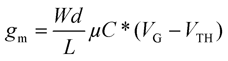
Although organic ECTs are different from FETs, it has been shown that the same equation as that used to describe electronic charge transport in long-channel FETs can be used for organic ECTs in the steady state.34–36 Specifically, the equation that describes transfer characteristics in a regime where doping occurs everywhere in the channel36 is given by:
 | (1) |
The main difference between the equations for ECTs and FETs is that the transconductance in ECTs scales with thickness and not just the channel area (i.e., W and L). This distinction arises since field-effect only modulates the channel at the semiconductor–insulator interface whereas redox doping modulates the carrier density throughout the bulk of the ECT channel.35,36
We therefore used this equation to calculate the mobility μ of different films in the transistor (Fig. 4b). In addition to μ, Fig. 4b also displays the variation in the maximum channel current with respect to d, showing a linear increase with thickness. The maximum calculated mobility was 0.036 cm2 V−1 s−1 – a comparable value to that measured for state-of-the-art organic ECT materials.37,38 The mobility values, however, decreased with a further increase in thickness (above 5 bilayers). Since capacitance and maximum channel current both show a linear increase with thickness, the decrease in mobility can only be related to the decrease in transconductance. Data show that indeed gm starts decreasing for thicknesses above 45 nm (Fig. 3e). Previous reports have shown that parasitic contact resistance limits ID,max, and consequently gm,max,37 for large Wd/L values. For the 2D ECTs reported here, W/L was 1000/20 μm, which could lead to saturation even at relatively low thicknesses above 45 nm. To verify this hypothesis, we have tested MXene ECTs (5 bilayer) with different W/L ratios (Fig. S14†). The data show that the maximum drain current and device hysteresis increase with the W/L ratio. Most importantly, the data confirm that gm saturates for a high W/L ratio, corroborating our hypothesis that contact resistance is the main factor behind gm saturation at high Wd/L values.
We note, however, that the mobility values are already good enough for some applications. The maximum ECT transconductance is also quite high, with an average value of 2.2 mS for 3 LbL MXene ECTs. Since MXene ECTs also operate at low threshold voltages Vth and the redox state of the channels is stable even when the gate voltage is turned off, these devices have low energy consumption when used as low power memory components, as in electrochemical random-access memories (ECRAMs) for neuromorphic devices.
Stable operation is an important parameter to consider when assessing device performance. We assessed the operational stability of 5 bilayer MXene ECTs by applying a square wave voltage to the gate electrode (from VG = 0 to 0.6 V) while monitoring the drain current at a constant drain voltage of VD = 0.5 V (Fig. S15†). MXene ECT devices show around 94.4% retention of the maximum drain current after 100 cycles.
2.4 The origin of conductance switching in MXene: correlating channel conductivity to electrochromism
Many mixed ionic/electronic conductors exhibit electrochromism,39 a reversible change in their optical properties due to a change in their redox state.Previous work has shown that Ti3C2Tx MXene thin films can undergo reversible changes in optical absorption upon electrochemical cycling in acidic electrolytes (H3PO4 and H2SO4) at potentials below 1 V (with silver wire as the reference electrode).40,41 Some MXenes may exhibit metal–insulator transition meditated by adsorbates induced by electrochemistry on their surface.42 Such an electrochromic effect is attributed to a non-faradaic electrical double layer as well as a faradaic redox process.43 In the case of acidic electrolytes, the main effect should be from the proton redox of Ti. To assess whether MXene ECTs could also operate in contact with aqueous electrolytes, we acquired 5 bilayer MXene ECTs using 0.1 M NaCl(aq) as the electrolyte (Fig. S16†). Data show that the aqueous electrolyte leads to similar MXene ECT operation with respect to the acid electrolyte, leading to an increase in the drain current upon the application of positive gate voltages. However, these devices led to the maximum transconductance gm,max value of 0.93 mS and an Ion/Ioff ratio of 1.4, with respect to the gm,max value of 2.76 mS and an Ion/Ioff ratio of 1.58 observed for the PVA-H2SO4 electrolyte. Overall, the data indicate that H+ ions are more effective than Na+ as doping ions in MXene ECTs.
For organic ECTs, it is known that ion–electron coupling, i.e. redox reactions, leads to the formation of charge carriers (e.g., polarons and bipolarons) in the conjugated polymer backbone, resulting in a change in its bandgap and conductivity.6 Here, we further correlate the phenomenon of changes in film conductance as observed in ECTs, by linking it to the optoelectrochemical behavior of LbL-assembled MXene.
To further consolidate our results, we compared the changes in optical absorbance at selected wavelengths as obtained from spectroelectrochemical measurements to the drain current obtained from ECT transfer characteristics (Fig. 4c and d). Previous work showed that redox potentials extracted from in situ UV-Vis spectroelectrochemistry correlate well with threshold voltage values extracted from ECT measurements.44–46 To ensure that the electrochemical potential can be matched between the experiments we used the same electrolyte and Ag/AgCl pseudoreference electrode for both types of measurements (see the schematic in Fig. 2a and 3a). The data show that the increase in drain current coincides with a decrease in absorbance of the plasmonic band (760 nm) and an increase of absorbance at a wavelength of 1095 nm. These data suggest that the reversible protonation of Ti (see the schematic in Fig. 3a) is responsible for both electrochromism and conductance change upon redox doping of the MXene film. This is to our knowledge the first report of correlating optoelectronic properties and electrochemical device performance in MXene films.
In addition, during ion intercalation processes, ions could physically expand the interlayer spacing, which may also lead to a change in the properties of the films. The combination of all these phenomena leads to changes in the overall optical (as probed by UV-Vis) as well as long-range electronic conductivity of the ECTs. Stability data show that this is indeed the case for LbL-assembled MXene ECTs, leading to a decrease in stability upon ON/OFF switching at VG values from 0 to 0.6 V (Fig. S15†). Future work should focus on a deeper understanding of these phenomena, which could be further modulated by the type of molecule used as an interlayer between MXene flakes as well as the chemical structure of the MXene.
3. Conclusion
The solid-state field-effect transistor, FET, and its theories were paramount in the discovery and studies of graphene. Here, we show that MXenes, a class of 2D materials beyond graphene, have mixed electronic–ionic properties that enable the realization of electrochemical transistors (ECTs). The current parameters of MXene ECTs show good normalized transconductance (12.5 S cm−1) but low on–off ratios (1.19), these values are already state of the art for use in devices like electrochemical random-access memories (ECRAMs) or biosensors.We further show that conductance switching data measured using ECTs in combination with other in situ electrochemical measurements (such as UV-Vis), is a powerful tool to correlate the changes in the device current to that of redox states; to our knowledge, this is the first report of this important correlation for MXene films.
Further studies beyond graphene 2D materials within the framework of ECTs are expected to enable the optimization of parameters, such as higher on–off ratios, very large channel currents, increasing transconductance, or extremely high switching speeds. Future experiments on Donnan permselectivity of the LbL MXene with different types of cationic spacers are expected to elucidate the impact of redox formal potential in LbL films on ECT operation.29 Spatiotemporal in situ optical measurements of the channel area will provide information on whether the so-called moving front effect,44 which has been shown for organic electronic material, is also present for 2D MXenes or other 2D materials.
Many future possibilities exist for MXene ECTs as over 30 different MXenes are predicted. We thereby foresee that even transition metal dichalcogenides (TMDs) and other bandgap materials can form ECTs and 2D iontronics. Future ECTs may also comprise heterostructure films with a mixture of MXenes and 2D TMDs.
2D ECTs can draw great inspiration and theoretical tools from the field of organic ECTs.47–49 They have the potential to considerably extend the capabilities of transistors beyond those of organic ECTs, as they have added properties such as extreme heat resistance, tolerance for solvents, and higher conductivity for both electrons and ions than organic mixed ionic/electronic conductors, such as conducting polymers.
4. Methods
4.1 Synthesis of MXene
The MAX phase was synthesized according to our previous work17 and powdered. MAX phase (Ti3AlC2) powder was delaminated in 2 g of LiF completely dissolved in 40 mL of 6 M HCl solution under constant stirring for 15 min. This was followed by the addition of 2 g of MAX phase powder at a rate of 200 mg min−1 in an ice bath. The etchant was maintained at 50 °C for 24 h at 550 rpm under constant stirring. The etchant was cooled to room temperature and washed several times with Millipore water until it reached pH ≈ 6. The obtained powders were dispersed in deaerated Millipore water and probe sonicated for 1 h in an ice bath. The dispersed solution was centrifuged at 3500 rpm for 1 h, the supernatant was collected, centrifuged at 5000 rpm, and re-dispersed in 10 mL Millipore water using vigorous shaking for 15 minutes to form the final MXene ink. The ink concentration was determined from the net weight of the MXene film obtained by vacuum filtration of a known volume of ink on a Celgard membrane.4.2 MXene characterization using SEM
We produced multilayered MXene films via both spin-coating and LbL-assembly techniques on Si substrates for SEM observations. Cross-sectional SEM images were obtained by field emission SEM (Hitachi S4800, Hitachi Corp., Japan).4.3 PVA-H2SO4 gel electrolyte synthesis
To purify absorbed air in the water, we bubbled 10 mL Milli-Q water with Ar gas for 1 h and used it to dissolve 1 g PVA (polyvinyl alcohol) (Sigma, Mw = 89![[thin space (1/6-em)]](https://www.rsc.org/images/entities/char_2009.gif) 000–98000, 99+% hydrolyzed). The solution was stirred at 85 °C on a hot plate for at least 3 hours until it became transparent, indicating that PVA is well dissolved. Sequentially, the prepared solution was removed from the hot plate and cooled down to room temperature. Concentrated H2SO4 (0.6 ml) (Sigma, >97.5%) was very slowly added to the PVA solution, followed by stirring for at least 1 h at room temperature.
000–98000, 99+% hydrolyzed). The solution was stirred at 85 °C on a hot plate for at least 3 hours until it became transparent, indicating that PVA is well dissolved. Sequentially, the prepared solution was removed from the hot plate and cooled down to room temperature. Concentrated H2SO4 (0.6 ml) (Sigma, >97.5%) was very slowly added to the PVA solution, followed by stirring for at least 1 h at room temperature.
4.4 ECT fabrication
We utilized two types of MXene multilayers as redox-active channels in our study: LbL-assembled and spin-coated MXene multilayers. Prior to multilayer formations, bare glass substrates were bath-sonicated in the sequence of acetone, ethanol, and isopropyl alcohol for 20 min each. Afterward, we patterned them with Cr (50 nm) and Au (150 nm) electrodes (channel dimensions, L = 20 μm, W = 1000 μm) using photolithography. Then, we treated O2 plasma (Optrel GBR, Multi-stop) for 20 min to create the hydrophilic surface to facilitate uniform coverage of 2D MXene for both cases.To avoid any parasitic capacitances from metal/electrolyte interfaces, we coated polymethyl methacrylate (PMMA) on the source–drain Au electrode after LbL-assembled MXene formation to complete ECT devices. To prepare PMMA solution, we dissolved 1 g poly(methyl methacrylate) (Sigma, Mw ≈ 996000 by GPC, crystalline) in 10 mL toluene (Sigma, ACS reagent, ≥99.5%), and the mixed solution was stirred vigorously at 80-degree celsius overnight.
For the spin-coated MXene multilayers, aqueous Ti3C2Tx MXene solution (2 g L−1) was coated at 3000 rpm for 30 seconds. This step was repeated 5, 10, or 20 times to form multilayers of increasing thickness.
In the case of LbL-assembled MXene multilayers, we used tris(3-aminopropyl)amine (TAPA, Sigma) as a spacer molecule to provide efficient interlayer chemistry. We prepared 1 bilayer (8.79 nm), 3 bilayers (26.38 nm), 5 bilayers (43.97 nm), 7 bilayers (61.55 nm), 10 bilayers (87.94 nm) and 12 bilayers (105.5 nm) of the MXene–TAPA bilayer. Prior to dipping the substrates, we used 3 M adhesive tape to prohibit the back-side coating of the substrate during the dipping process. We treated the substrate surface by using O2 plasma for 15 min to modify its wetting properties and as-treated substrates were then loaded into a dipping robot (StratoSequence VI, nanoStrata Inc.). For the LbL assembly setup, aqueous Ti3C2Tx MXene dispersion (2 g L−1) and TAPA dissolved in Milli-Q water (1 g L−1) were used. We performed 8 consecutive dipping steps including rinsing with pure Milli-Q water using an automated program (StratoSmart v7.0). For one cycle, i.e., one bi-layer formation, the substrates were firstly dipped into TAPA-dissolved solution and sequentially spun in a circle for 5 min. Subsequently, they were rinsed repeatedly 3 times, 2 min each. After the formation of positive charges on the surface, the substrates were dipped and spun again in the negatively charged MXene solution for 5 min and rinsed repeatedly 3 times for 2 min. These steps were repeated for the formation of MXene multilayers. We then dried the LbL assembled films overnight in a vacuum oven at room temperature. To prevent any parasitic capacitances from the undesired Au bottom electrode, we dropcast a solution of PMMA, (Sigma, Mw ∼ 996000 by GPC, crystalline) on the edge of the dried MXene film. The gel electrolyte was then dropcast on top of LbL-assembled MXene multilayers. Finally, the Ag/AgCl pellet was dipped in the gel electrolyte to complete the electrochemical transistor configurations.
4.5 ECT data collection and characterization
We measured transistor data using a Keithley 4200A-SCS parameter analyser in the air at room temperature. Data analysis was performed using Origin Pro 2020. Transconductance data (calculated by using the following equation: gm = ∂ID/∂VG) were smoothed by adjacent averaging to attenuate instrument and environment noise. We calculated the threshold voltage using the extrapolation in the linear region (ELR) method. This method calculates the threshold voltage by finding the gate voltage axis intercept of the linear extrapolation of the IDversus VG curve at its maximum first derivative point.4.6 In situ spectroelectrochemistry
An ITO glass slide coated with MXene served as the working electrode. Pt coil was used as the counter electrode and Ag/AgCl pellet was used as the reference electrode. The three-electrode cells were dipped together in 1 M PVA-H2SO4 electrolytes in a standard quartz cuvette, located in the middle of beam path of an ultraviolet–visible (UV–vis) spectrophotometer (PerkinElmer LAMBDA 750 UV/Vis/NIR spectrophotometer). For the in situ setup, we used three connected electrodes for cyclic voltammetry (CV) and recorded the corresponding optical absorption as a function of applied potential with a step of 0.1 V.4.7 Impedance measurements
MXene films were deposited via LbL assembly on square gold electrodes of dimension 2 mm2. For electrode fabrication, a glass wafer was cleaned via subsequent ultrasonication in soapy water for 15 minutes, basic piranha cleaning in a solution of H2O:H2O2:NH3 at around 70 °C for 5–10 minutes, and O2 plasma for 15 min. Gold contacts were prepared by evaporation using a custom-made paper mask50 to form a 10 nm-thick chromium layer as an adhesion layer and a 50 nm-thick gold layer.
EIS measurements were performed on the LbL-assembled MXene using a BioLogic VSP potentiostat. The MXene films on gold were used as the working electrode, an Ag/AgCl pellet pseudo reference was used as the reference electrode, and a platinum coil as a counter electrode The electrolyte was 1 M poly(vinyl alcohol) (PVA) in H2SO4, for the ECTs. EIS data were acquired at frequencies between 100 kHz and 10 Hz at a sinus amplitude of 10 mV and a potential of −0.8 V. The capacitance was extracted by fitting the data to a modified Randles circuit model Rs(Rp||Q), where Rs is the electrolyte resistance, Rp is the charge transfer resistance, and Q is a constant phase element, using ZFit (EC-Lab V11.41 software). The thickness of the films was determined in a dry state from the SEM cross-section images.
4.8 CV measurements and calculation of capacitance
CV measurements were performed on LbL-assembled MXene using a BioLogic VSP potentiostat with the same setup as that used for EIS measurements. The CV curves were obtained at a scan rate of 100 mV s−1. The specific capacitance C (F cm−2) was estimated by using eqn (2)51 | (2) |
4.9 Free standing MXene membranes
MXene membranes were prepared by mixing MXene with cellulose nanofibers (CNF). The MXene-CNF dispersions were vacuum-filtered into sheets using a microfiltration assembly with Durapore PVDF membranes and dried for 15 min using a Rapid Köthen sheet drier (Paper Testing Instruments, Austria) at 93 °C and a reduced pressure of 95 kPa. The dried sheets were cut into suitable sizes (length 2.5 cm, width 0. 5 cm) for use as the gate for ECT devices.Conflicts of interest
There are no conflicts to declare.Acknowledgements
MinA acknowledges funding from ÅForsk project 18-461. J. S. acknowledges funding from Olle Engkvists Stiftelse, project 213-0253. M. H. acknowledges funding from Swedish Energy Agency (Energimyndigheten), project 48489-1. This project has received funding from the European Union's Horizon 2020 Research and Innovation program under the Marie Sklodowska-Curie grant agreement No 101025599. E. Z. gratefully acknowledges the Göran Gustafsson Foundation, the Swedish Research Council (Grant No. 2022-02855), and Formas - a Swedish Research Council for Sustainable Development (Grant No. 2022-00374) for support. This work was supported by AIMES - The center for integrated medical and engineering sciences (www.aimes.se), Karolinska Institutet (1-249/2019), KTH Royal Institute of Technology (VF-2019-0110), and Getinge AB (4.1599/2018). This work was partially supported by the Wallenberg Initiative Materials Science for Sustainability (WISE) funded by the Knut and Alice Wallenberg Foundation.References
- K. S. Novoselov, A. K. Geim, S. V. Morozov, D. Jiang, Y. Zhang, S. V. Dubonos, I. V. Grigorieva and A. A. Firsov, Science, 2004, 306, 666–669 CrossRef CAS PubMed.
- V. Nicolosi, M. Chhowalla, M. G. Kanatzidis, M. S. Strano and J. N. Coleman, Science, 2013, 340, 1226419 CrossRef.
- N. Mounet, et al. , Nat. Nanotechnol., 2018, 13, 246–252 CrossRef CAS PubMed.
- M. Naguib, V. N. Mochalin, M. W. Barsoum and Y. Gogotsi, Adv. Mater., 2014, 26, 992–1005 CrossRef CAS PubMed.
- A. V. Mohammadi, J. Rosen and Y. Gogotsi, Science, 2021, 372, 6547 Search PubMed.
- W. Choi, N. Choudhary, G. H. Han, J. Park, D. Akinwande and Y. H. Lee, Mater. Today, 2017, 20, 116–130 CrossRef CAS.
- Y. Liu, X. Duan, H. J. Shin, S. Park, Y. Huang and X. Duan, Nature, 2021, 591, 43–53 CrossRef CAS PubMed.
- D. Nilsson, M. Chen, T. Kugler, T. Remonen, M. Armgarth and M. Berggren, Adv. Mater., 2002, 14, 51–54 CrossRef CAS.
- E. Zeglio and O. Inganas, Adv. Mater., 2018, 30, 18800941 CrossRef PubMed.
- J. Rivnay, S. Inal, A. Sallea, R. M. Owens, M. Berggren and G. G. Malliaras, Nat. Rev. Mater., 2018, 3, 17086 CrossRef CAS.
- J. H. Bombile, M. J. Janik and S. T. Milner, Phys. Chem. Chem. Phys., 2018, 20, 317–331 RSC.
- J. T. Friedlein, R. R. McLeod and J. Rivnay, Org. Electron., 2018, 63, 398–414 CrossRef CAS.
- H. Sun, J. Gerasimov, M. Berggren and S. Fabian, J. Mater. Chem. C, 2018, 6, 11778–11784 RSC.
- M. M. Hamedi, R. Forchheimer and O. Inganäs, Nat. Mater., 2007, 6, 357–362 CrossRef CAS PubMed.
- E. Zeglio, A. L. Rutz, T. E. Winkler, G. G. Malliaras and A. Herland, Adv. Mater., 2019, 31, 1806712 CrossRef PubMed.
- P. Gkoupidenis, N. Schaefer, B. Garlan and G. G. Malliaras, Adv. Mater., 2015, 27, 7176–7180 CrossRef CAS PubMed.
- A. Melianas, M. A. Kang, A. V. Mohammadi, T. J. Quill, W. Tian, Y. Gogotsi, A. Sello and M. M. Hamedi, Adv. Funct. Mater., 2022, 32, 2109970 CrossRef CAS.
- B. Xu, M. Zhu, W. Zhang, X. Zhen, Z. Pei, Q. Xue, C. Zhi and P. Shi, Adv. Mater., 2016, 28, 3333–3339 CrossRef CAS PubMed.
- W. Tian, A. V. Mohammadi, Z. Wang, L. Ouyang, M. Beidaghi and M. M. Hamedi, Nat. Commun., 2019, 10, 2558 CrossRef PubMed.
- X. Xu, H. Zhang, Q. Diao, Y. Zhu, G. Yang and B. Ma, J. Mater. Sci.: Mater. Electron., 2020, 31, 175–181 CrossRef CAS.
- J. K. El-Demellawi, S. Lopatin, J. Yin, O. F. Mohammed and H. N. Alshareef, ACS Nano, 2018, 12, 8485–8493 CrossRef CAS PubMed.
- P. Salles, D. Pinto, K. Hantanasirisakul, K. Maleski, C. E. Shuck and Y. Gogotsi, Adv. Funct. Mater., 2019, 29, 1809223 CrossRef.
- B. D. Paulsen, K. Tybrandt, E. Stavrinidou and J. Rivnay, Nat. Mater., 2020, 19, 13–26 CrossRef CAS PubMed.
- M. M. Hamedi, K. Tvingstedt, R. H. Karlsson, P. Åsberg and O. Inganäs, Nano Lett., 2009, 9, 631–635 CrossRef CAS PubMed.
- P. Nayak, Q. Jiang, R. Mohanraman, D. Anjum, M. N. Hedhili and H. N. Alshareef, Nanoscale, 2018, 10, 17030 RSC.
- D. Mawad, P. J. Molino, S. Gambhir, J. M. Locke, D. L. Officer and G. G. Wallace, Adv. Funct. Mater., 2012, 22, 5020–5027 CrossRef CAS.
- R. Shameem, L. M. Bongartz, A. Weissbach, H. Kleemann and K. Leo, Appl. Sci., 2023, 13(9), 5754 CrossRef CAS.
- D. Ohayon, V. Druet and S. Inal, Chem. Soc. Rev., 2023, 52, 1001 RSC.
- E. J. Calvo and A. Wolosiuk, J. Am. Chem. Soc., 2002, 124, 8490–8497 CrossRef CAS PubMed.
- A. M. Pappa, S. Inal, K. Roy, Y. Zhang, C. Pitsalidis, A. Hama, J. Pas, G. G. Malliaras and R. M. Owens, ACS Appl. Mater. Interfaces, 2017, 9, 10427–10434 CrossRef CAS PubMed.
- Y. Peng, B. Akuzum, N. Kurra, M. Q. Zhao, M. Alhabeb, B. Anasori, E. C. Kumbur, H. N. Alshareef, M. D. Ger and Y. Gogotsi, Energy Environ. Sci., 2016, 9, 2847 RSC.
- N. Kurra, B. Ahmed, Y. Gogostsi and H. N. Alshareef, Adv. Funct. Mater., 2016, 6, 1601372 Search PubMed.
- C. Zhang, M. P. Kromer, A. S. Ascaso, S. H. Park, N. McEvoy, B. Anasori, Y. Gogotsi and V. Nicolosi, Adv. Funct. Mater., 2018, 28(9), 1870059 CrossRef.
- D. A. Bernards and G. G. Malliaras, Adv. Funct. Mater., 2007, 17, 3538–3544 CrossRef CAS.
- S. Inal, G. G. Malliaras and J. Rivnay, Nat. Commun., 2017, 8, 1767 CrossRef PubMed.
- J. Rivnay, et al. , Sci. Adv., 2015, 1(4), e1400251 CrossRef PubMed.
- P. R. Paudel, V. Kaphle, D. Dahal, R. K. R. Krishnan and B. Lussem, Adv. Funct. Mater., 2021, 31, 2004939 CrossRef CAS.
- H. Sun, M. Vagin, S. Wang, X. Creipin, R. Forchheimer, M. Berggren and S. Fabiano, Adv. Mater., 2018, 30, 1704916 CrossRef PubMed.
- P. Chandrasekhar, B. J. Zay, G. C. Birur, S. Rawal, E. A. Pierson, L. Kauder and T. Swanson, Adv. Funct. Mater., 2002, 12, 95–103 CrossRef CAS.
- J. Li, et al. , ChemElectroChem, 2021, 8, 151–156 CrossRef CAS.
- Y. Liu, S. P. Jiang and Z. Shao, Mater. Today Adv., 2020, 7, 100072 CrossRef.
- K. D. Fredrickson, B. Anasori, Z. W. Seh, Y. Gogotsi and A. Vojvodic, J. Phys. Chem. C, 2016, 120, 28432–28440 CrossRef CAS.
- C. Zhan, M. Naguib, M. Lukatskaya, P. R. Kent, Y. Gogotsi and D. E. Jiang, J. Phys. Chem., 2018, 9, 1223–1228 CAS.
- E. Stein, O. Nahor, M. Stolov, V. Freger, L. M. Petruta, I. McCulloch and G. L. Frey, Nat. Commun., 2022, 13, 5548 CrossRef CAS PubMed.
- Y. Wang, et al. , Adv. Funct. Mater., 2022, 32, 2111439 CrossRef CAS.
- G. E. Fenoy, C. Bilderling, W. Knoll, O. Azzarini and W. A. Marmisolle, Adv. Electron. Mater., 2021, 7, 2100059 CrossRef CAS.
- E. Stavrinidou, M. Sessolo, B. W. Jensen, S. Sanaur and G. G. Malliaras, AIP Adv., 2014, 4, 017127 CrossRef CAS.
- D. Tu and S. Fabiano, Appl. Phys. Lett., 2020, 117, 080501 CrossRef CAS.
- A. V. Volkov, K. Wijeratne, E. Mitraka, U. Ail, D. Zhao, K. Tybrandt, J. W. Andreasen, M. Berggren, X. Crispin and I. V. Zozoulenko, Adv. Funct. Mater., 2017, 27, 1700329 CrossRef.
- F. E. Nik, I. Matthiesen, A. Herland and T. Winkler, Micromechanics, 2020, 11(7), 676 Search PubMed.
- W. Zhang, Y. Tan, Y. Gao, J. Wu, B. Tang and J. Zhao, RSC Adv., 2014, 4, 27800–27804 RSC.
Footnotes |
| † Electronic supplementary information (ESI) available. See DOI: https://doi.org/10.1039/d3nr06540e |
| ‡ These authors contributed equally to this work. |
| This journal is © The Royal Society of Chemistry 2024 |