
 Open Access Article
 This Open Access Article is licensed under a Creative Commons Attribution-Non Commercial 3.0 Unported Licence
Electrical properties of disordered films of van der Waals semiconductor WS2 on paper†
Fatima Zahra
Kharchich
 ab,
Andres
Castellanos-Gomez
c and
Riccardo
Frisenda
*a
ab,
Andres
Castellanos-Gomez
c and
Riccardo
Frisenda
*a
aPhysics Department, Sapienza University of Rome, Piazzale Aldo Moro 5, 00185 Rome, Italy. E-mail: riccardo.frisenda@uniroma1.it
bPhysics Department, Abdelmalek Essaadi University, M'haneche II, 93002 Tetouan, Morocco
cMaterials Science Factory, Instituto de Ciencia de Materiales de Madrid (ICMM-CSIC), Madrid E-28049, Spain
First published on 12th April 2024
Abstract
One of the primary objectives in contemporary electronics is to develop sensors that are not only scalable and cost-effective but also environmentally sustainable. To achieve this goal, numerous experiments have focused on incorporating nanomaterial-based films, which utilize nanoparticles or van der Waals materials, on paper substrates. In this article, we present a novel fabrication technique for producing dry-abraded van der Waals films on paper, demonstrating outstanding electrical characteristics. We assess the quality and uniformity of these films by conducting a spatial resistivity characterization on a 5 × 5 cm2 dry-abraded WS2 film with an average thickness of 25 μm. Employing transfer length measurements with varying channel length-to-width ratios, we extract critical parameters, including sheet resistance and contact resistance. Notably, our findings reveal a resistivity approximately one order of magnitude lower than previous reports. The film's inherent disorder manifests as an asymmetric distribution of resistance values for specific geometries. We explore how this behavior can be effectively modeled through a random resistance network (RRN), which can reproduce the experimentally observed resistance distribution. Finally, we investigate the response of these devices under applied uniaxial strain and apply the RRN model to gain a deeper understanding of this process.
 Riccardo Frisenda | RF earned his PhD title from TU Delft in 2016 under the supervision of Prof. van der Zant with a thesis about electrical transport through single-molecules contacted by movable nano-electrodes. After his PhD, RF moved as a postdoc to the laboratory of Dr. Castellanos-Gomez in IMDEA Nanoscience and later in the Instituto de Ciencia de Materiales de Madrid (ICMM) to study optoelectronics devices based on 2D materials, strain in 2D materials and 2D metal-2D semiconductor interfaces. In 2022 RF moved back to his Alma Mater, La Sapienza University, where he currently investigates spectroscopy in 2D materials and 2D device physics. |
Introduction
Electronic sensors have become ubiquitous in the modern society since they are fundamental in many technological and economic areas, from the production of smartphones and cars, to manufacturing and logistics. Also, novel applications such as electronic skins, human–machine interfaces or the internet of things are completely based on electronic sensors.1–5 Thus, one of the present world challenges is the fabrication of sensors that are scalable, inexpensive, and environmentally friendly. For this reason, many researchers focused on the combination of paper, which is a biodegradable and inexpensive substrate, with films based on nanomaterials, such as nanoparticles or van der Waals (vdW) materials.6,7 To this end the typical fabrication approach found in the literature is based on depositing the electronic material of choice on a paper substrate through inkjet printing or solution dipping.8,9 One recently demonstrated alternative strategy is the direct abrasion of van der Waals materials on paper, which allows to fabricate films without the need of solvents, thus reducing both the impact on the environment and the fabrication costs.10,11 This method, which has been demonstrated first with graphite (from pencils), has been extended only recently to other van der Waals materials, such as semiconducting MoS2 or WS2 or superconducting NbSe2.12,13Achieving highly conductive films using ink suspensions containing vdW materials is challenging, due to the presence of solvent-related adsorbates on the deposited vdW materials that reduce the coupling between platelets.9,14–17 In contrast, films fabricated from the direct abrasion method using a manually operated cotton swab, have already demonstrated outstanding electrical properties, with improvements of the film resistivities of more than one order of magnitude compared to vdW inks.18 In this work we demonstrate a fabrication method capable of improving the film electrical resistivity based on the use of an electric drill with a modified spherical drill bit to deposit the vdW powder on paper. This setup allows to fabricate homogenous and large area (larger than 5 × 5 cm2) films of WS2 or MoS2 on paper in a relatively short time, which, thanks to the solvent-free processing, yields a disordered network of intimately interconnected platelets. Transfer length methods measurements performed in a statistical way give a resistivity ρ = 19.7 Ωm and contact resistance RC = 0.13 MΩ, which to our knowledge are the lowest values reported in literature for disorder WS2 thin films and are more than one order of magnitude lower than previous reports.18 Our electrical results can be reproduced by a random resistor network (RRN) solved by a combination of Ohm's law and Kirchhoff's circuit law, which capture the essential physics of these disordered films such as the intrinsic device-to-device variation.19,20 We also demonstrate the strain sensing capabilities of our devices by subjecting them to controlled uniaxial strain and discuss the results using the RRN model.
Results and discussion
To fabricate large area WS2 thin films we exploit the dry abrasion of APS micronized WS2 in powder form (Hagen Automation Ltd, average platelet size of 0.6 μm) on standard A4 copy paper (80 g m−2) as substrate. Fig. 1a shows the steps to deposit a 5 × 5 cm2 film of WS2 on paper, firstly we mask the deposition area (1) and then we rub the WS2 powder using an electric drill with a modified spherical drill bit (2). The standard spherical ceramic stone drill bit is wrapped by eight layers of polyester knitted wipers (RS Pro, 162-5686) to allow deformation in the drill bit and achieve a more homogenous pression. The film can then be drawn quickly (3) and the final appearance is shiny and rather homogenous (4). From an inspection with an optical microscope operated in reflection or transmission illumination mode, in Fig. 1b, the film appears optically homogenous apart from a gradient, visible in transmission illumination mode, about 200 μm long in the region that separates the film from the bare paper substrates. To measure the thickness of the film, which is needed to determine its resistivity, we slice the film with a sharp razor blade and using a calibrated optical microscope we inspect the cross-section. Fig. 1c shows the cross-section of the film that appears rather homogenous with a thickness of 20 μm and Fig. 1d shows an histogram of the thicknesses estimated from 16 different cross-sections. The average thickness is t = (25 ± 6) μm, which confirms the homogeneity of the final films.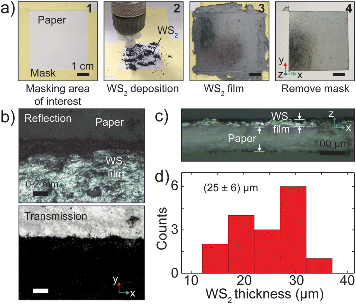 | ||
| Fig. 1 Fabrication of large-area WS2 films by the dry-abrasion method on paper. (a) Fabrication process of a 5 × 5 mm2 WS2 film on paper. (b) Optical microscopy image of the edge of the WS2 film on paper and part of the uncovered paper substrate, taken in reflection illumination mode (top) and transmission (bottom). (c) Optical microscopy image of the cross section of the WS2 film on paper. (d) Histogram of the WS2 extracted from cross section microscopy images. | ||
After depositing the film we test the electrical properties of the film such as its resistivity by depositing graphite electrodes onto the film. Fig. 2a shows the electrode deposition and the electrical testing setup. Firstly we draw an array of graphite electrodes using an 8B pencil separated by 5 mm one from the other (1) and labelled with numbers 1,2…9. By varying this separation we can achieve different channel lengths. We then cut, using a sharp razor blade, the film in the direction perpendicular to the electrodes in 5 mm wide ribbons (2) labelled with letters a, b…i. In this way we obtain 81 different devices with channel length L = 5 mm and channel width W = 5 mm, which, thanks to the labelling, can be spatially localized in the film. We then proceed to recording the resistance of each device using two electrical probes supported by a magnet to achieve reproducible probe pressure, as shown in (3). After fabrication we recorded the individual resistance (at a low constant voltage of 0.1 V) of each of the 81 devices finding values in the 0.5 to 2.7 MΩ range. Fig. 2b shows these resistance values as a colormap where black regions correspond to low resistance devices and yellow/white to large resistance ones. Thanks to the device labelling this colormap gives information on the spatial homogeneity of the electrical properties of the WS2 film. As can be seen, the film homogeneity is good on a few cm scale demonstrating the capabilities of the proposed deposition method in producing large area films. Fig. 2c shows an histogram of the resistance values taken from the map in panel b, which shows a peak at low resistance values and a tail at larger resistance values. We fit this histogram to a log–normal distribution, which accounts for the fact that the resistance R is positive bounded, using the formula  . From the fitting parameters we can calculate the mode of the distribution according to M = exp(μ − σ2). From the fit we find μ = −0.077 MΩ and σ = 0.25 MΩ which gives a resistance R(L = 5 mm) = (0.87 ± 0.25) MΩ.
 | ||
| Fig. 2 Electrical characterization of WS2 films on paper. (a) Deposition of graphite electrodes (pencil 8B) on the WS2 film on paper and electrical characterization. (b) Color map of the measured resistance of the WS2 film on paper (channel length L and width W both equal to 5 mm). (c) Histogram of the resistances calculated from the values in panel (b). (d) Transfer length method representation of the resistance of the WS2 film versus the channel length (W = 5 mm) where the circles are the individual data points, and the thick black lines represent the mode and the standard deviation of each set of data points. The linear fit (red line) allows to extract the contact resistance (Rc) and the sheet resistance (Rs) of the film. | ||
The resistance properties of the fabricated films can be extracted through a transfer length measurement. To do this we repeated the previous fabrication four additional times increasing the channel length in steps of 5 mm. Note that given the larger channel length each time we decreased the number of fabricated devices. For each set of resistance values R(L) we bin the values in a histogram and fit it to the log–normal distribution. Fig. 2d shows the results of this procedure where the resistance is plotted as a function of the channel length. The colored circles correspond to the resistances values of all the devices and the black horizontal and vertical bars represent respectively the distribution mode and standard deviation of each channel length calculated from the fitting parameters. The mode values increase from 0.86 MΩ to 4 MΩ when increasing the channel length from 5 mm to 25 mm and the standard deviation increases as well. From this set of mode values at different lengths we extract the contact resistance RC and the sheet resistance RS of the film (see inset of Fig. 2d for a circuit diagram) by performing a linear fit to these points. In the fitted linear equation the slope is equal to RS/W and the intercept with the vertical axis to 2RC. The red line in Fig. 2d is the result of such a fit from which we find RS = 0.79 MΩ □−1 and RC = 0.13 MΩ. Finally, using the just found RS value and the thickness t (estimated in Fig. 1d) we can calculate the resistivity ρ according to ρ = RSt and we find ρ = 19.7 Ωm. To our knowledge this resistivity is the lowest value reported in literature for WS2 films on paper fabricated by dry abrasion or by liquid phase exfoliated inks.18,21 Compared to the in-plane conductivity of bulk or of single-layer WS2 obtained by mechanical exfoliation,22,23 this resistivity value is still more than three orders of magnitude larger. This suggests that the out-of-plane and the flake-to-flake transport play a significant role in the total resistance of the WS2 films on paper. On the other hand, RC is comparable to previous reports for WS2 films contacted by graphite electrodes suggesting that it does not depend on the film itself but rather on the graphite–WS2 interface.18,24,25
To understand the origin of the resistance distribution and model the transport through the disordered WS2 films we propose a random resistor network (RRN) model,26,27 which we used in a previous article to model the superconducting transport transition in a disordered film of NbSe2 on paper.12Fig. 3a shows a schematic of the physical devices and a zoomed-in sketch of the WS2 film composed of interconnected WS2 platelets. Here, one can identify two components to the film resistance, a lower intra-platelet resistance (RIntra) and a larger inter-platelet one (RInter). A crude model of the film can then be given by a two-dimensional network of RIntra and RInter resistances with low valued resistance elements (RElectrodes) at the two sides to simulate the graphite electrodes (and used to apply voltage uniformly to the film). The right panel of Fig. 3a shows an example of a small RRN composed of 36 voltage nodes and 60 resistances.
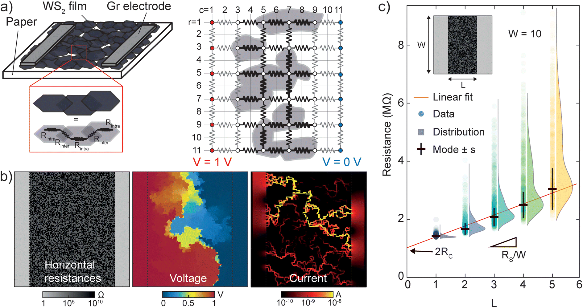 | ||
| Fig. 3 Random resistance network model. (a) Schematic of the van der Waals film on paper (left) and random resistance network (RRN) composed of low valued resistance elements at the two sides to simulate the electrodes, and a random mixture of medium and large ones to simulate the channel (right). This network is composed by 6 × 6 = 36 voltage nodes and 5 × 6 + 5 × 6 = 60 horizontal and vertical resistor elements. (b) Left: RRN composed of 150 × 150 resistors. Center: voltage across the RRN calculated with boundary conditions V = 1 V on the far-left side and V = 0 V on the far-right side. Right: current density calculated from the resistance and voltage maps. (c) Transfer length method simulated using RRNs with channel width W = 10 and different channel lengths. The resistance of each RRN is represented by the circles and the distributions of these resistances is shown on the right of the data points as a half-violin plot. | ||
To model mathematically the RRN we construct a Nx × Ny matrix (with Nx = 2nx − 1 and Ny = 2ny − 1, where nx and ny are the number of voltage nodes across the x and y directions), which contains the resistance and the voltage values. The resistance elements occupy the positions identified by the indexes r = 1, 3, 5…Nx and c = 2, 4, 6…Ny − 1 (for horizontally oriented resistors) or r = 2, 4, 6…Nx − 1 and c = 1, 3, 5…Ny (for vertically oriented resistors). The voltage nodes are located at the positions r = 1, 3, 5…Nx and c = 1, 3, 5…Ny. Note that given nx × ny voltage nodes, the number of resistors can be calculated according to: (2nx − 1)×(2ny − 1) − nx × ny − (nx − 1) × (ny − 1). We populate the matrix with binomial distributed random resistances in the channel and low resistances at the left and right sides. In the case of the left panel of Fig. 3b, a RRN with nx = ny = 100, we choose RIntra = 105 Ohm, RInter = 1010 Ohm and Relectrodes = 1 Ohm. These values for the resistance can be considered as effective values used to reproduce the general physics of the problem and not to simulate the specific film. Notice that in the chosen RRN geometry, the length L and width W of the channel are well defined geometrical quantities. To finish the setting-up of the simulation we apply a fixed voltage to the left and right electrodes by assigning the desired voltage values at the right positions (in the showed case VLeft = 1 V and VRight = 0 V respectively).
To solve for the network unknown voltages and currents we use the Kirchoff's node law combined to the Ohm's law in matrix form. To account for these two laws we create a new matrix, of size approximately nx2 × ny2, that represents a system of linear equations where the unknowns are the voltages across the network. We then solve for the voltages using the linear equations solver in MATLAB (version R2022b, MathWorks) and then calculate the current across each resistor element. Fig. 3b central and right panels show the results for the voltages and the magnitude of the current flowing through the RRN presented in the left panel. We can see that the voltage is constant in each electrode as expected and that the voltage drop has a step-like behavior, with islands of approximately constant voltage appearing. The logarithmic map of the current shows a filament behavior where few parallel paths contribute mostly to the total current flowing through the RRN, and most of the RRN resistors carry a negligible current. Notice that this behavior is typical of percolative networks of different nature.28,29 From this current map we find the total current flowing in the RRN (and the total resistance of the network), calculated by summing all the currents flowing through a column of horizontal resistors (i.e. summing all the currents with indexes r = 1, 3, 5…Nx and c = Ny/2).
To assess statistically the distribution of the total resistance in a given RRN geometry, we simulate hundreds of randomly generated RRNs and construct the histogram of the total resistance found in each case. To simulate the transfer length discussed in Fig. 2, we generate different RRNs with fixed width W = 10 and varying lengths L = 5, 10, 15, 20, 25 (see the inset of Fig. 3c). For each L we generate and solve hundreds of RRNs and we plot the results in Fig. 3c as a scatter plot (for the individual resistances) combined with a half violin plot to show the total histogram of each L. From this graph we can see that the resistances for a given L show a distribution peaked at lower resistance and with a tail at larger resistance values. This behavior is comparable with the one found from the histograms of the transfer length resistances of Fig. 2c. Similar to the experimental case, we characterize the different distributions by their mode and standard deviation. Interestingly, by increasing L the mode increases in an approximately linear fashion and the standard deviation also increases, similar to the experimental observations.
Being paper an easily deformable material, one possible application of electrical devices based on films on paper is in strain sensing.25,30 In the following we discuss the strain sensing capabilities of our devices and show how the RRN model can give some insight into the physical process behind the strain sensing in disordered films. We start by characterizing a WS2 drawn channel contacted by graphite drawn electrodes and subjected to uniaxial (compressive or tensile) strain using the apparatus shown in the inset of Fig. 4a. The use of linear micromanipulators allows to finely tune the radius of curvature R of the device and thus the strain. We calculate the strain using the formula 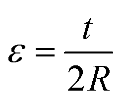 , where t is the thickness of the device (approximately 100 μm, see Fig. 1c). For each value of strain we record the resistance of the device and we plot the results in Fig. 4a. The unstrained device has a resistance of R0 = 2.03 MΩ, which decreases for compressive strain and increases for tensile strain. The rate of change in the resistance as a function of strain is commonly referred to as gauge factor (GF) which is calculated as GF = (R − R0/R0)/ε = (ε/R0)/ε.5,25Fig. 4b shows ΔR/R0versus epsilon for two different devices based on WS2 with unstrained resistances respectively R0 = 1.83 MΩ (red circles) and R0 = 2 MΩ (orange circles). In these two devices the data shows a linear increase with applied strain symmetric for tensile and compressive strain. We find GF = 100 by performing a linear regression to the data. Fig. 4c shows similar measurements performed on a MoS2 film based device. The devices in this case show a much larger unstrained resistance of R0 = 7 GΩ and R0 = 11 GΩ, in accordance with previous reports on MoS2 films on paper fabricated with similar methods.11 These resistance values are around two orders of magnitude larger than those of large-area MoS2 films deposited on SiO2/Si with Au prepatterned electrodes (L = 10 μm, W = 1000 μm) where square resistances are in the order of 5–50 MΩ □−1 compared to our MoS2 film where the film resistance is 1000 MΩ □−1.31 This difference could be due to the different production method of MoS2 that in ref. 31 comes from mechanically exfoliated flakes from bulk MoS2 and in our case comes from MoS2 micronized powder. Interestingly, while the lower R0 device shows similar slopes both for tensile and compressive strain with a GF = 100, the larger R0 device shows a smaller slope for compressive strain in respect to the tensile train datapoints. In this last device we find GF = 100 for tensile strain and GF = 10 for compressive strain.
 | ||
| Fig. 4 Strain sensors based on van der Waals materials on paper. (a) Resistance versus (tensile and compressive) uniaxial strain curves for a WS2 device. Inset: photograph of the strain setup with superimposed the estimated radius of curvature R. (b) Percentage change in the device resistance for two different WS2 devices versus uniaxial strain. (c) Same as (b) for two different MoS2 devices. (d) RRN network simulations of films with high density (left) and low density (right) under compressive and tensile strain. The lower panels show the calculated current flowing in the networks. (e) Summary of the gauge factor versus uniaxial strain calculated in four different simulations at increasing film density (blue high density and red low density films). | ||
In order to gain more insight on the strain sensing properties of disordered films we apply the RRN model. In this case, to simulate disordered films and apply strain we generate a network of randomly placed squares which we can individually track and displace independently one from the other. The top row of Fig. 4d shows two resistance networks generated in this way, on the left for a larger number (or density) of squares and on the right for a lower number of squares. The central panel in each of the two cases correspond to the unstrained network. The left and right panel of each case correspond respectively to compressive and tensile strained networks. The bottom row shows the calculated current in each case. For the unstrained case we see the usual behavior of RRN where current is carried mostly through a few “filaments” in parallel. The high density network does not show strong change in the number of current paths as a function of strain meaning that also the total resistance does not depend strongly on the strain and thus the gauge factor is small (lower than 10). On the other hand, the low density RRN shows a strong dependency of the current paths on the strain. From the bottom right panel of Fig. 4d it is clear how for compressive strain the network shows a large number of parallel current paths while for tensile strain the current paths are less and carry overall a much lower current. This can give a strong modulation of the total resistance versus strain for tensile strain and larger gauge factors (larger than 10). Fig. 4e summarizes the results from four different simulation performed for increasing RRN densities.
Conclusions
In conclusion, we demonstrated the fabrication of large-area films of van der Waals semiconductor WS2 on paper by using a modified dry abrasion method. The resistivity of a film of size 5 × 5 cm and thickness of approximately 25 μm sampled in 81 locations shows a good spatial uniformity demonstrating the good quality of the produced film. By performing transfer length measurements with L/W ranging from 1 to 5 we extract the sheet resistance and the contact resistance of the films finding R and R, with Rs being one order of magnitude lower than previous reports. The disordered nature of the film, composed of a network of interconnected WS2 platelets, shows up in an asymmetric distribution of resistance values for a certain L/W geometry. This behavior is consistent with the percolative nature of the WS2 resistance network as showed by a random resistance network model. We found that in a network composed of two resistances (a smaller one and a larger one, respectively interpreted as an intra-flake and an inter-flake resistance), randomly scattered in a square lattice, the observed distribution of the resistances is similar to the one observed experimentally with a peak at low resistance values and a tail at larger resistance values. Interestingly, both experimentally and theoretically a lower scattering in the resistance of the film, measured from the standard deviation of the distribution, is observed for devices with smaller L/W. Finally we discuss the behavior of these devices under applied uniaxial strain and we applied the RRN model to understand the process. The RRN simulations at different film densities show that the in the low density limit larger gauge factors can be achieved due to the formation of cracks in the film that can lead to rupture and remodulation of conductive paths.Conflicts of interest
The authors declare no competing financial interests.Acknowledgements
This project was partially funded by the PRIN Grants 2D-FRONTIERS (20228879FT) and 2D-PentaSensing (P2022HT3FF) of Ministero dell'Università e della Ricerca (MUR), by Sapienza University Ateneo funds “Progetti di Ricerca Medi” 2022 and by the Ministry of Science and Innovation (Spain) through the projects PID2020-115566RB-I00 and PDC2023-145920-I00.References
- S. R. Forrest, The path to ubiquitous and low-cost organic electronic appliances on plastic, Nature, 2004, 428(6986), 911–918 CrossRef CAS PubMed
.
- F. V. Paulovich, M. C. F. De Oliveira and O. N. Oliveira Jr., A future with ubiquitous sensing and intelligent systems, ACS Sens., 2018, 3(8), 1433–1438 CrossRef CAS PubMed
- M. Bariya, H. Y. Y. Nyein and A. Javey, Wearable sweat sensors, Nat. Electron., 2018, 1(3), 160–171 CrossRef
- H. Nazemi, A. Joseph, J. Park and A. Emadi, Advanced micro-and nano-gas sensor technology: A review, Sensors, 2019, 19(6), 1285 CrossRef CAS PubMed
- P. A. Vermeulen, J. Mulder, J. Momand and B. J. Kooi, Strain engineering of van der Waals heterostructures, Nanoscale, 2018, 10(3), 1474–1480 RSC
- Y. Zhang, L. Zhang, K. Cui, S. Ge, X. Cheng, M. Yan, J. Yu and H. Liu, Flexible electronics based on micro/nanostructured paper, Adv. Mater., 2018, 30(51), 1801588 CrossRef PubMed
- A. J. Magdaleno, R. Frisenda, F. Prins and A. Castellanos-Gomez, Broadband-tunable spectral response of perovskite-on-paper photodetectors using halide mixing, Nanoscale, 2022, 14(38), 14057–14063 RSC
- Z. Lin, Y. Huang and X. Duan, van der Waals thin-film electronics, Nat. Electron., 2019, 2(9), 378–388 CrossRef
- K. Cho, T. Lee and S. Chung, Inkjet printing of two-dimensional van der Waals materials: a new route towards emerging electronic device applications, Nanoscale Horiz., 2022, 7(10), 1161–1176 RSC
- D. Nutting, J. F. Felix, E. Tillotson, D.-W. Shin, A. De Sanctis, H. Chang, N. Cole, S. Russo, A. Woodgate and I. Leontis, Heterostructures formed through abraded van der Waals materials, Nat. Commun., 2020, 11(1), 3047 CrossRef CAS PubMed
- A. Mazaheri, M. Lee, H. S. Van Der Zant, R. Frisenda and A. Castellanos-Gomez, MoS 2-on-paper optoelectronics: drawing photodetectors with van der Waals semiconductors beyond graphite, Nanoscale, 2020, 12(37), 19068–19074 RSC
- J. Azpeitia, R. Frisenda, M. Lee, D. Bouwmeester, W. Zhang, F. Mompean, H. S. Van Der Zant, M. García-Hernández and A. Castellanos-Gomez, Integrating superconducting van der Waals materials on paper substrates, Mater. Adv., 2021, 2(10), 3274–3281 RSC
- T.-L. Ren, H. Tian, D. Xie and Y. Yang, Flexible graphite-on-paper piezoresistive sensors, Sensors, 2012, 12(5), 6685–6694 CrossRef CAS PubMed
- D. J. Finn, M. Lotya, G. Cunningham, R. J. Smith, D. McCloskey, J. F. Donegan and J. N. Coleman, Inkjet deposition of liquid-exfoliated graphene and MoS 2 nanosheets for printed device applications, J. Mater. Chem. C, 2014, 2(5), 925–932 RSC
- G. Cunningham, M. Lotya, N. McEvoy, G. S. Duesberg, P. van der Schoot and J. N. Coleman, Percolation scaling in composites of exfoliated MoS 2 filled with nanotubes and graphene, Nanoscale, 2012, 4(20), 6260–6264 RSC
- A. G. Kelly, D. O'Suilleabhain, C. Gabbett and J. N. Coleman, The electrical conductivity of solution-processed nanosheet networks, Nat. Rev. Mater., 2022, 7(3), 217–234 CrossRef CAS
- S. Barwich, J. M. de Araújo, A. Rafferty, C. G. da Rocha, M. S. Ferreira and J. N. Coleman, On the relationship between morphology and conductivity in nanosheet networks, Carbon, 2021, 171, 306–319 CrossRef CAS
- M. Lee, A. Mazaheri, H. S. Van Der Zant, R. Frisenda and A. Castellanos-Gomez, Drawing WS 2 thermal sensors on paper substrates, Nanoscale, 2020, 12(43), 22091–22096 RSC
- A. B. Harris and R. Fisch, Critical behavior of random resistor networks, Phys. Rev. Lett., 1977, 38(15), 796 CrossRef
- G. Ahmed and J. Blackman, On theories of transport in disordered media, J. Phys. C: Solid State Phys., 1979, 12(5), 837 CrossRef CAS
- D. O'Suilleabhain, V. Vega-Mayoral, A. G. Kelly, A. Harvey and J. N. Coleman, Percolation effects in electrolytically gated WS2/graphene nano: nano composites, ACS Appl. Mater. Interfaces, 2019, 11(8), 8545–8555 CrossRef PubMed
- M. Agarwal, P. Patel and O. Vijayan, Electrical studies on (Mo/W) Se2 single crystals. I. Electrical resistivity, Phys. Status Solidi A, 1983, 78(1), 133–136 CrossRef CAS
- D. Ovchinnikov, A. Allain, Y.-S. Huang, D. Dumcenco and A. Kis, Electrical transport properties of single-layer WS2, ACS Nano, 2014, 8(8), 8174–8181 CrossRef CAS PubMed
- W. Zhang, Q. Zhao, C. Munuera, M. Lee, E. Flores, J. E. Rodrigues, J. R. Ares, C. Sanchez, J. Gainza and H. S. van der Zant, Integrating van der Waals materials on paper substrates for electrical and optical applications, Appl. Mater. Today, 2021, 23, 101012 CrossRef
- W. Zhang, R. Frisenda, Q. Zhao, F. Carrascoso, A. M. Al-Enizi, A. Nafady and A. Castellanos-Gomez, supported WS2 strain gauges, Sens. Actuators, A, 2021, 332, 113204 CrossRef CAS
- J. P. Straley, Critical phenomena in resistor networks, J. Phys. C: Solid State Phys., 1976, 9(5), 783 CrossRef
- V. V. Cheianov, V. I. Fal'ko, B. L. Altshuler and I. L. Aleiner, Random resistor network model of minimal conductivity in graphene, Phys. Rev. Lett., 2007, 99(17), 176801 CrossRef PubMed
- N. Araújo, P. Grassberger, B. Kahng, K. Schrenk and R. M. Ziff, Recent advances and open challenges in percolation, Eur. Phys. J.: Spec. Top., 2014, 223, 2307–2321 Search PubMed
- S. Kirkpatrick, Percolation and conduction, Rev. Mod. Phys., 1973, 45(4), 574 CrossRef
- X. Liao, Z. Zhang, Q. Liao, Q. Liang, Y. Ou, M. Xu, M. Li, G. Zhang and Y. Zhang, Flexible and printable paper-based strain sensors for wearable and large-area green electronics, Nanoscale, 2016, 8(26), 13025–13032 RSC
- Y. Sozen, J. J. Riquelme, Y. Xie, C. Munuera and A. Castellanos-Gomez, High-Throughput Mechanical Exfoliation for Low–Cost Production of van der Waals Nanosheets, Small Methods, 2023, 7(10), 2300326 CrossRef CAS PubMed
Footnote |
| † Electronic supplementary information (ESI) available. See DOI: https://doi.org/10.1039/d3nr06535a |
| This journal is © The Royal Society of Chemistry 2024 |