
 Open Access Article
 This Open Access Article is licensed under a Creative Commons Attribution-Non Commercial 3.0 Unported Licence
Effects of radiation damage on the yielding and fracture of nanowires†
Daniel
Vizoso
 and
Rémi
Dingreville
*
and
Rémi
Dingreville
*
Center for Integrated Nanotechnologies, Sandia National Laboratories, 1515 Eubank Blvd NE, Albuquerque, NM 87123, USA. E-mail: rdingre@sandia.gov
First published on 19th January 2024
Abstract
Since free surfaces act as perfect sinks for radiation-induced defects, nanowires, owing to their high surface-to-volume ratio, are considered to be radiation tolerant. But the question remains on how this tolerance translates to their yielding and fracture behavior. Atomistic simulations of irradiated gold nanowires reported here show the existence of a size regime where the yield stress is affected by the accumulation of radiation damage. Our analysis also shows that, regardless of the diameter of the nanowire, early on during tensile loading, much of the radiation-induced defect content initially present in the wire is rapidly cleaned by the motion of pre-existing dislocations as well as dislocations emitted from the surface of the wire. This defect removal process resets the crystallographic configuration of the wire which subsequently deforms and fractures via the same mechanisms that occur in pristine, un-irradiated nanowires. We conclude that the fracture behavior of nanowires in the size and dose regimes tested is unaffected by radiation damage.
1. Introduction
The fracture of nano-sized objects remains hard to predict using classical continuum fracture theory due to surface effects and the confinement of deformation mechanisms that are not present at higher length scales. The fracture of nanowires under tension has been explored both computationally and experimentally across a wide range of states, including wire shapes and diameters,1–8 crystalline phases and orientations,1,5,8,9 aspect ratios,10,11 temperatures,1,12 and strain rates.4,10,13 For example, Wang et al.4 performed many molecular dynamics simulation trials for gold (Au) nanowires of various lengths and cross-sectional areas under tension, and noted a size dependence on the first yield stress and first yield strain, as well as a large variance in the position of fracture depending on both the cross-sectional area of the nanowires and the strain rate. Ojeda et al.7 developed a high-throughput experimental methodology for examining the fracture of silver (Ag) nanowires under tension and observed size-dependent probability distributions for fracture strains. Sun et al.11 performed molecular dynamics simulations of twinned copper (Cu) nanowires and observed that the failure modes of the nanowires transitioned between brittle fracture to ductile fracture, depending on the length of the nanowires as well as the spacing between twin boundaries that had been inserted into the nanowires. Beets et al.14 used a combination of atomistic simulations and experimental characterization to investigate fracture in nanoporous Au, showing that the strength of ligaments (which can be approximated as nanowires) depends on their orientation and morphology. Regarding the fracture mechanism, they showed the localization of deformation to a narrow zone of ligaments, where individual ligaments would fail via a necking mechanism. The fracture process predicted by their molecular dynamics simulations replicated those observed experimentally with fairly good accuracy.14Investigations into how the structural characteristics of nanowires alter their behaviors have not been limited to just mechanical properties. Radiation tolerance is another property that has been observed to exhibit a length-scale dependence.15–19 We recently showed that the mechanisms for radiation damage accumulation in nanowires depend on their diameter, with some nanowires exhibiting unique damage mechanisms that are not observed in structures with different length scales and others showing little to no defect accumulation at all.19 In addition, we showed that some of these mechanisms are potentially reversible upon mechanical loading for specific size regimes.20 However, one critical question remains: how does radiation damage affect the yielding and fracture behavior of nanowires? In bulk materials, radiation damage can lead to increased embrittlement and reduced ductility.21 However, in the case of nanowires, while radiation effects can introduce defects and change the structure of the wire (e.g. phase transformation or roughening of the surface of the wire due to sputtering, see ref. 19), they may inhibit or exacerbate certain deformation and fracture mechanisms. For instance, Jia et al.22 performed molecular dynamics simulations of the tensile loading of gallium arsenide (GaAs) nanowires after consecutive ion strikes and observed significant changes in the Young's modulus and yield properties as a function of total dose and irradiation conditions. One of the primary reasons for these changes was associated with amorphization of the wire under radiation. Several studies have explored the impact of single radiation damage events on the Young's modulus and yield behavior of Cu nanowires, with their primary focus being an examination of how the energy of the damage event23–26 or pre-strain applied before the damage event occurs26 changes the defect structures produced in the wire, which in turn alters the mechanical performance of the wires. In this paper, we go beyond the effect of single ion strikes and investigate how radiation damage accumulation due to many consecutive events affects yielding and fracture in metallic nanowires. We performed a series of molecular dynamics simulations on Au nanowires of various diameters under tension with and without the presence of radiation damage, for damage levels up to a maximum dose of approximately one displacement per atom (dpa). This survey, both in terms of size and damage level, enables us to examine how radiation damage alters the yielding and fracture behavior of nanowires across a broad range of length scales and radiation damage states.
2. Methods
We performed a series of molecular dynamics simulations using the Large-scale Atomic/Molecular Massively Parallel Simulator (LAMMPS).27,28 We used an Embedded Atom Method (EAM) interatomic potential developed by Foiles et al.29 to describe the atomic interactions in the Au wires. Our simulation geometries consisted of cylindrical Au nanowires of diameters of 3, 7, 10, 14, and 20 nm, with all of the simulated nanowires having lengths equal to twice their diameters to keep the aspect ratio constant. We used accelerated multi-cascade atomistic simulations (consecutive cascades for the 3 nm and 7 nm diameter wires and the reduced-order atomic cascade (ROAC) model30,31 for the bigger wires) to simulate the accumulation of radiation-induced damage in these wires. Details of the procedure utilized for simulating radiation damage accumulation in these nanowires can be found in Vizoso et al.,19 with a short summary provided in Note 1 of the electronic supplementary information (ESI).†For each nanowire size, we chose several damage levels to serve as the initial defected structures for the fracture simulations. For the 3 and 7 nm diameter nanowires, we chose five different damage states: the pristine nanowires as well as structures after 26, 51, 76, and 100 consecutive cascades. For the larger nanowires (diameters of 10, 14, and 20 nm), we chose six different damage states: the pristine structures as well as structures with damage levels of 0.05, 0.25, 0.50, 0.75, and 0.99 dpa. These damage levels were chosen to sample the different regimes of defect accumulation mentioned in ref. 19. In contrast to small nanowires, wires with diameters of 10 nm and greater require higher damage levels for their structures to be changed significantly by radiation damage.
Prior to the application of tensile strain, we equilibrated each of those nanowire structures at 300 K and zero pressure for a minimum of 50 ps under an isothermal-isobaric ensemble (NPT). Periodic boundary conditions were maintained along the primary axis of the nanowire for all molecular dynamics simulations. We then applied tensile strain using the fix deform command in LAMMPS along the primary axis of the nanowire, which corresponded with the [001] FCC direction of the pristine nanowires. Periodicity was maintained along the primary axis of the nanowires during the application of tensile strain. Fig. 1(a) shows a render of a 10 nm diameter nanowire with the loading direction illustrated with arrows. A constant engineering strain rate of 1 × 10⁻⁴ ps−1 (1 × 10⁸ s−1) was used for all tension simulations. During the application of tensile strain, each structure was maintained at a constant temperature of 300 K under a canonical ensemble (NVT). For each nanowire diameter and damage level tested, we performed three independent fracture simulations by evolving the structures under an NVT ensemble maintained at 300 K for an additional 50 and 100 ps prior to the application of tensile strain. The tensile strain was applied until fracture was achieved, which varied across the set of structures tested in this work. In total, we performed 84 simulations. For each of these simulations, we measured the stress state of the nanowires by summing the z-component of the per-atom stress tensor computed by LAMMPS over all of the atoms in the simulations and dividing that sum by the volume of the nanowire as measured by the compute surface mesh32 modifier in OVITO.33 We measured dislocation densities using the DXA34 modifier in OVITO. We measured the Young's modulus for each nanowire by computing the slope of the initial linear portion of the stress versus strain data for each fracture simulation, as illustrated by the triangle in Fig. 1(e).
 | ||
| Fig. 1 (a) Render of a 10 nm diameter nanowire, with blue arrows indicating the direction of deformation, (b) stress versus strain for a 10 nm diameter nanowire under tension, (c) dashed vertical line indicating the yield point, (d) dashed vertical line indicating the fracture point, and (e) triangle whose slope is equal to the Young's modulus. | ||
3. Results
3.1. Yield and fracture mechanisms of un-irradiated nanowires
Fig. 1(b) shows a typical stress–strain response for a 10 nm diameter Au nanowire under tension. Across all pristine, un-irradiated nanowires simulated for this work, the stress initially increased linearly with strain within the elastic regime, after which, at some size-dependent strain (see Section 2), the wire undergoes an initial yield event, which involves the emission of dislocations from the surface, which then proceeded to glide along 〈111〉 planes and form stacking faults across the wire. Dislocations were emitted from multiple points along the surface of the nanowire, with the number of dislocations emitted increasing as the diameter of the nanowire was increased. These multiple emissions resulted in complex stacking-fault and dislocation structures immediately after the initial yield, with the number of stacking faults also increasing as the initial diameter of the nanowire increases. We refer the reader to Videos 1–5 provided as ESI† for an animated illustration of this process for unirradiated nanowires with diameters of 3, 7, 10, 14, and 20 nm, respectively. This initial yielding mechanism matches the behavior observed by Beets et al.14 for the simulations they performed of the fracture of nanoporous Au using the same interatomic potential used in this work, as well as the behavior observed by Park and Zimmerman10 for the simulations that they performed of Au nanowires with a different interatomic potential. After this initial yield, these pristine nanowires are deformed via consecutive discrete events as illustrated by the series of small stress increases and drops with additional strain in the stress–strain curves, with each of these drops corresponding to either the emission of dislocations from the surface or changes to the internal stacking fault and dislocation network within the wire, resulting in either the formation or removal of stacking faults, or the formation of nanotwins across the diameter of the wire. This predicted yielding mechanism by our simulations corresponds to the one observed experimentally by Lu and coworkers9 in sub-20 nm Au nanowires. Again, the reader is referred to ESI Videos 1–5† for animated illustrations of these mechanisms.Fracture of pristine nanowires occurred via two observed mechanisms. In a vast majority of the simulations of the un-irradiated nanowires, fracture occurred via a slip mechanism, where consecutive yield events would occur along the same crystallographic plane, typically next to a stacking fault. As these slip events continue to occur, the wire shears and eventually fractures. This mechanism is illustrated in Fig. 2(a–d) for a 10 nm diameter nanowire, with ESI Videos 2–5† showing this fracture mechanisms for wires with initial diameters of 7, 10, 14, and 20 nm, respectively. Again, this predicted mechanism corresponds to the experimentally observed fracture mechanism in Au nanowires by Lu and coworkers,9 as well as the simulations performed by Sun et al.11 of the ductile fracture of twinned Cu nanowires. In a few of the tension simulations, typically for wires with a small diameter (3 to 7 nm), the wires yielded via a necking mechanism. This fracture mechanism only occurred in structures that had undergone the formation of a nanotwin across the diameter of the wire, but not all wires that formed nanotwins fractured via this mechanism. Fig. 2(e–h) illustrates a 3 nm diameter nanowire failing via this mechanism, with ESI Video 1† showing the evolution of this mechanism in time for the 3 nm diameter nanowire shown in Fig. 2(e–h). In ESI Video 1† and Fig. 2(e–h), we note that some stacking faults near the necking region are perpendicular to the primary axis of the nanowire, such that shearing along a stacking fault plane is no longer possible. These two fracture processes can be considered as a form of ductile fracture, with none of the pristine wires fracturing via a brittle fracture mechanism. This result aligns with the observations made by Sun et al.11 for the fracture of Cu nanowires with pre-existing twins as well as initially pristine nanowires, where the same ductile fracture mechanisms were observed in all of the nanowire diameters that they tested with lengths below 130 nm.
 | ||
| Fig. 2 Renders of the tensile deformation of a 10 nm diameter nanowire (a–d) and a 3 nm diameter nanowire (e–h), with strains being marked next to the renders. Atoms are colored according to their structure type as determined by OVITO: cyan atoms are FCC, red are HCP, white are disordered. Half of the disordered surface atoms have been removed for clarity. | ||
3.2. Size dependence of the mechanical properties in un-irradiated nanowires
The size dependence for various mechanical properties for pristine Au nanowires (with diameters of 3, 7, 10, 14, and 20 nm) is plotted in Fig. 3 as a function of the inverse diameter of the wire. Fig. 3(a) shows that the Young's modulus is inversely proportional to the diameter of the nanowire. We observe the opposite trend for the yield strain and stress as shown in panels (c) and (d), and no obvious relationship between the strain at fracture and the diameter of the nanowires as seen in panel (b). | ||
| Fig. 3 Size effects for (a) Young's modulus, (b) fracture strain of pristine nanowires, (c) yield strain, and (d) yield stress under tension versus inverse nanowire diameter. | ||
The size dependence of the elastic behavior is explained by the role of residual surface stresses (in the Gibbsian sense) and the increasing surface-to-volume ratio as the diameter of the nanowires gets smaller.35,36 Regarding the yield stress, for nanowires with diameters greater than 3 nm, the maximum stress coincides with the yield stress, while for the case of the 3 nm diameter nanowire, the maximum stress was reached at some point after the first yield event. Generally speaking, we observe that the yield stress decreases as the diameter of the nanowire increases until reaching a plateau that begins at a diameter of 10 nm. For wires with bigger diameters, increasing the diameter does not correlate with an additional decrease in the yield stress or the maximum stress. This size effect is related to a decrease of surface dislocation density with decreasing diameter.37,38 Additionally, this effect of surface dislocation density is accompanied by deformation twinning which further exacerbates the size dependence of the yield stress.39,40 Similar size effects on yielding have been observed experimentally not only in Au nanowires9,41 but also in other metallic nanowires.42
Regarding the lack of size dependence for the strain at fracture, rather than interpreting the lack of visible correlation between the observed fractures strains and the nanowire diameters as a lack of correlation altogether, we instead estimate that the number of simulations performed was insufficient to capture the mean values of the expected distributions. Indeed, previous experimental7 and computational4 studies have shown that fracture properties (such as fracture strain or fracture position along the nanowire) do correlate with the diameter of nanowires to some extent with broad distributions that can obfuscate trends without sufficient data to properly capture the mean and the variance of these distributions. Size dependence on the fracture of nanowires has been observed experimentally37,43 albeit for much bigger diameters in the sub-micron scale as well as much lower strain rates.
3.3. Size-dependent radiation damage in nanowires
Before discussing how radiation damage potentially changes the yielding and fracture mechanisms in nanowires discussed in the sections above, we briefly review the different size-dependent mechanisms of damage accumulation in irradiated nanowires.19Fig. 4 shows the defect structures created in irradiated nanowires from the three different size regimes for defect accumulation.19 | ||
Fig. 4 Renders of the defect structures produced (a) a 7 nm diameter nanowire after 100 consecutive cascades, (b) a 10 nm diameter nanowire at 0.99 dpa, and (c) a 20 nm diameter nanowire at 0.05 dpa. Structures are not rendered to scale. Atoms are colored according to their structure type as determined by OVITO: red are HCP, white are disordered. Half of the disordered surface atoms and all FCC atoms have been removed for clarity. Dislocations are colored according to their type: green are  , magenta are , magenta are  . . | ||
For very small nanowires with a diameters less than 10 nm, the primary degradation mechanism under irradiation is sputtering, see Fig. 4(a). In this range of small sizes, the tolerance of nanowires to radiation damage is rather unstable. In this case, increasing damage results primarily in the formation of surface craters incurred by consecutive ion strikes and spread out throughout the surface of the nanowire. In addition to sputtering, the small nanowires can also experience amorphization of the entire wire or a region of the wire upon being struck by consecutive cascades. This amorphization is a direct consequence of the size of the thermal spike from the ion strikes relative to the small size of the wire. Further details on this sputtering mechanism are provided in our previous work.19 Larger nanowires (i.e. with diameters greater or equal to 10 nm) also experience some sputtering, but because of the decrease in the surface to volume ratio with increasing size, surface roughening and sputtering become less dominant damage mechanisms. For these larger nanowires, the dominant radiation damage mechanism is the formation and accumulation of point defects, defect clusters, dislocation loops, and stacking fault tetrahedras (SFTs) (see panel (c) in Fig. 4). As the diameters of the nanowires continue to increase, the evolution of defect densities approach those of bulk materials. More details on this mechanism are also provided in our previous work.19 Finally, the last mechanism only exists for a narrow range of wire diameters around 10 nm for which the wire experiences a FCC-to-HCP phase transformation with increasing radiation damage. This transformation is initiated via the formation of radiation-induced stacking-fault lamellas developing across the wire which subsequently pile up with increasing radiation damage. This pile-up mechanism is equivalent to a gradual phase transformation (see panel (b) in Fig. 4 as well as our previous work19 for a detailed description and visualizations of this mechanism).
3.4. Effect of radiation damage on the yield and fracture behavior of nanowires
Fig. 5 shows the yield stress and fracture strain for the range of tested nanowire diameters as a function of the total number of consecutive cascades for the 3 and 7 nm diameter nanowires and the total dose for the 10, 14, and 20 nm diameter nanowires. An equivalent figure for the evolution of the yield strain and Young's Modulus for irradiated nanowires of various diameters is provided in Note 2 of the ESI.† Across the entire dataset (Fig. 5(a, c, d, e, g and i)), with the exception of some of the low damage level states of the 3 nm diameter nanowire, we note that the introduction of radiation damage results in a reduction in the yield stress compared to the pristine, un-irradiated wire. For the 3 nm diameter nanowire (Fig. 5(a)) case past 25 cascades and for the 7 nm diameter nanowire (Fig. 5(c)), we observe a trend where increasing the number of consecutive cascades prior to the application of tension results in a decrease of the yield stress. As mentioned in ref. 19, the 3-to-7 nm in diameter corresponds to a size regime where sputtering is the dominant damage mechanism. In this case, radiation-induced surface roughening facilitates the emission of dislocations from the surface of the wire, resulting in the reduced yield stress in this size regime with increasing radiation damage. See ESI Videos 6 and 7† for visualization of this mechanism in a 3 nm diameter nanowire after 50 consecutive cascades and a 7 nm diameter nanowire after 100 consecutive cascades, respectively. For nanowires with diameters of 10 nm or greater (Fig. 5(e, g and i)), where the effect of sputtering is expected to be much smaller, there is no clear dose dependence observable for the yield stress and therefore larger wires are less susceptible to reducing their yield stress with increasing radiation damage. In these cases, the presence of pre-existing radiation-induced defects in the bulk of the nanowires reduces the amount of stress necessary to initiate yield. Further increasing the radiation-induced damage in the wire does not substantially change the yield since the density of pre-existing dislocations and point-defect concentration remains relatively constant with increasing dose.19 Trends for the first yield strain, which are plotted in Fig. S1 in the ESI,† are less consistent, with radiation damage generally reducing the first yield strain with occasional simulations having first yield strains that were greater than those of the pristine structures. ESI Videos 8–13† provide visualizations of the yield and fracture mechanisms for irradiated nanowires with initial diameters of 10, 14, and 20 nm for two different damage states each. | ||
| Fig. 5 Yield stresses and fracture strains for nanowires at various damage levels, with the corresponding diameter for each row being marked in the top right corner of the yield stress plots. | ||
For the 3, 7, 14, and 20 nm diameter nanowires, no clear trends emerge between the fracture strain and the diameters of the nanowires or the damage levels prior to the application of tensile strain, with most of the data points in Fig. 5(b, d, f, h and j) showing no change to the fracture strain at all. For the 10 nm diameter nanowire (Fig. 5(f)), there does appear to be a decreasing trend in fracture strain as dose increases, with the highest dose point being consistently lower than the other points.
Through an examination of the fracture processes of the irradiated nanowires, we found no significant changes to the fracture mechanisms due to the presence or density of radiation damage. Fig. 6 shows the stress versus strain and dislocation density versus strain as well as renders of representative irradiated structures with diameters of 3 nm and 14 nm. In both simulations rendered for Fig. 6 and animated in ESI Videos 6 and 11,† respectively, the wires yield via the slip mechanism, where consecutive slip events occurred along a specific 〈111〉 plane until the wire had fractured.
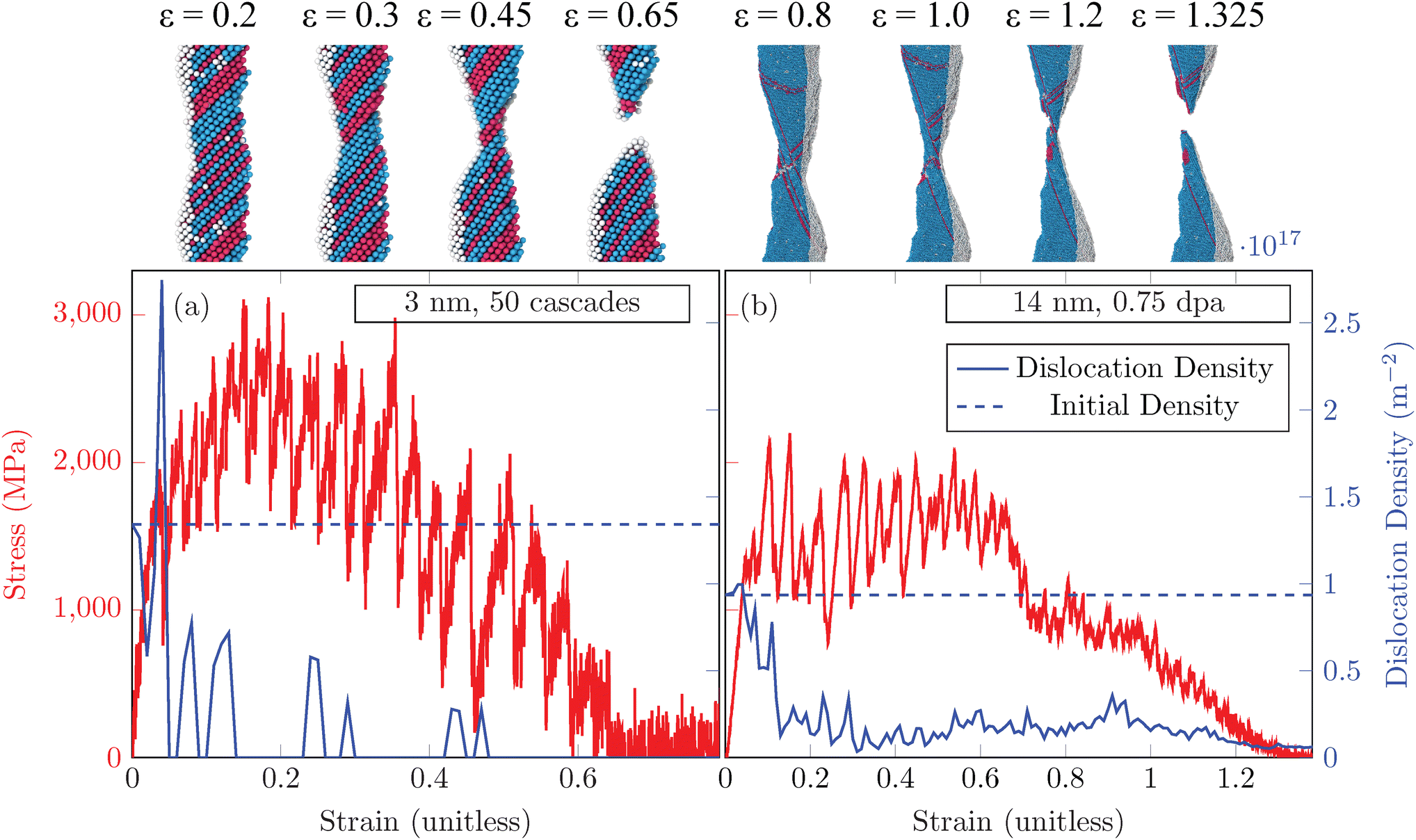 | ||
| Fig. 6 (a) and (b) Stress versus strain and dislocation density versus strain for two irradiated nanowire configurations. The diameter and dose are marked on each plot. Red lines show the stress, blue lines show the dislocation density. The dashed blue line shows the dislocation density prior to the application of strain. Above each plot, renders of the tensile deformation of the nanowires at several strain states are provided. Atoms are colored according to their structure type as determined by OVITO: cyan atoms are FCC, red are HCP, and white are disordered. Half of the disordered surface atoms have been removed for clarity. | ||
The nanowire with an initial diameter of 10 nm irradiated to 0.99 dpa underwent a radiation-induced phase transformation from FCC to HCP,19 as seen in Fig. 4(b). The presence of the HCP phase, in the form of thick layers of HCP planes along the 〈111〉 direction, drastically changes the mode of deformation of the wire (including in the elastic regime) until fracture. Indeed, as illustrated in Fig. 7(a), the Young's modulus of the nanowire is substantially larger due to the presence of the HCP phase at the dose of 0.99 dpa than the Young's modulus at lower doses prior to the initiation of the radiation-induced phase transformation. Subsequently, as seen in panel (b), under tensile loading, the HCP phase is stable and does not convert back to FCC. Under these conditions, the phase-transformed nanowire initially yields through slip events near the boundaries of the thick layers of HCP planes, resulting in a thinning of the cross section of the nanowire.20 As the wire is strained more, it experiences a change to the stacking faults near the thinned point, changing the yielding mechanism from slip along a 〈111〉 plane to a necking mechanism, which progresses through the rest of the renders to the fracture of the wire. The yield and fracture process of the 10 nm diameter nanowire at 0.99 dpa is animated in ESI Video 9.†
 | ||
| Fig. 7 (a) Young's modulus as a function of dpa for the 10 nm diameter Au nanowires and (b) stress versus strain and HCP phase fraction versus strain for a 10 nm diameter nanowire at 0.99 dpa. The red line shows the stress, and the blue line shows the HCP phase fraction. Above (b), renders of the tensile deformation of the nanowires at several strain states are provided. Atoms are colored according to their structure type as determined by OVITO: cyan atoms are FCC, red are HCP, and white are disordered. Half of the disordered surface atoms have been removed for clarity. | ||
3.5. Deformation and fracture mechanisms in irradiated nanowires
As was observed in the previous section, little to no correlation was observed between the yield or fracture parameters and the dose or the number of consecutive cascades for many of the irradiated nanowires. To develop an understanding of why defect types and densities play a limited role in the yielding and fracture behavior of nanowires under tension, an understanding of how those defect densities evolve as the nanowires are strained is required. Fig. 8 shows representative stress versus strain and dislocation density versus strain plots for several nanowires of various diameters and total doses. In these plots, we observe that the initial stages of the application of tension result in significant reductions in the dislocation density. This behavior was observed across the entire regime of nanowire diameters and dose levels tested. The smaller nanowires (diameters of 7 nm and 10 nm in Fig. 8(a) and (b)) see a complete removal of all dislocations prior to the first yield event, while larger nanowires (diameters of 14 nm and 20 nm in Fig. 8(c) and (d)), see a more gradual reduction in dislocation density, hitting a minimum prior to a strain of 0.2. This difference in the defect removal rate is likely related to the size dependence observed in the defect accumulation behavior of nanowires noted in ref. 19, where Au nanowires with diameters below 10 nm saw little to no internal defects form under irradiation while nanowires with larger diameters did accumulate dislocations and other defects such as SFTs. We note nonetheless that our atomistic simulations involve high strain rates and thus many thermally activated processes, such as vacancy diffusion along dislocation cores, are excluded from the simulations. The origin of this defect removal process is the interaction of pre-existing defects with dislocations moving through the wire during the deformation process. Indeed, given the confinement of the radiation-induced defects within the wire, even if the total number of defects is low, the probability that these defects interact with the dislocations emitted from the surface or those emitted during the dissociation of pre-existing defects such as SFTs into dislocations and stacking faults44 during tensile loading is high. As those dislocations rapidly move across the width of the wire, they promote the annihilation of the pre-existing, radiation-induced defects. In fact, this mechanism is analogous to the mechanisms of dislocation–defect cluster interactions45 and the formation of defect-free channels46–48 observed in bulk irradiated materials. In the case of nanowires, the probability of having defect–dislocation interactions gets higher as the diameter of the wire gets smaller. Animations of the tensile loading of irradiated nanowires of various diameters and at various doses, including the wires shown in Fig. 8, are provided as ESI Videos 6–13.† | ||
Fig. 8 (a–d) Stress versus strain and dislocation density versus strain for several nanowire configurations. The diameter and dose are marked on each plot. Red lines show the stress, and blue lines show the dislocation density. The dashed blue line shows the dislocation density prior to the application of strain. The dotted blue line shows the dislocation density evolution for a pristine, un-irradiated nanowire of the same diameter. (e–h) Renders of the initial defect structures present in the nanowires from (a–d) as well as renders of the nanowires post defect removal. Stars present in (a–d) indicate the strain of the post-defect removal structure. Render in (e) corresponds with plot (a), (f) with plot (b), (g) with plot (c), and (h) with plot (d). Half of the surface atoms as well as the FCC atoms have been removed to expose the interior defect structure. Atoms are colored according to their structure type: white is disorder, red is HCP. Dislocations are colored according to their type: green are  , magenta are , magenta are  . For (g) and (h), disordered atoms from the bulk of the nanowire have been removed. . For (g) and (h), disordered atoms from the bulk of the nanowire have been removed. | ||
After the initial loading phase where defects are removed, the nanowires at different dose levels evolve in essentially the same way due to their defect content, resulting in no observable correlation between the dose level and the yield and fracture parameters. Dislocation densities after the initial defect removal period are also similar to the dislocation densities observed in the pristine nanowire simulations, as indicated by the solid and dotted blue lines, respectively, in Fig. 8. For the nanowires that did see a dose dependence in the yield stress (those being the 3, 7, and 10 nm diameter nanowires in Fig. 5), it is likely that the source of this dose dependence is the reduction in nanowire diameter and roughening of the surface due to sputtering. This effect is known to become less dominant as the size of the nanowire increases, which can be seen in the fact that the magnitude of the dose effect on yield stress does decrease as nanowire diameter increases, and by the fact that no dose effect is observed for nanowire with diameters greater than 10 nm. In a similar fashion, the concentration or presence of radiation damage was not found to alter the yielding mechanism of the nanowires across the range of diameters tested, with the irradiated wires also experiencing ductile fracture in a similar manner to the pristine nanowires. Again, animations of the yielding and fracture process for nanowires of various damage levels and initial diameters are provided as Videos 1–13, with Note 3 in the ESI† providing a short description of each video.
4. Conclusion
The atomistic simulations of irradiated Au nanowires reported above showed a size dependence on some of their mechanical properties. The yield stress decreases with the introduction of radiation damage regardless of the initial diameter of the nanowire. Smaller nanowires (diameters of less than 10 nm) saw additional reduction in the yield stress with increasing radiation damage, while nanowires with larger initial diameters did not see a further decrease in their yield stress with additional radiation damage. For all of the tested nanowire sizes and damage levels without a phase transformed region, fracture behavior remained the same, both in terms of the fracture mechanisms as well as the fracture strain. We attribute this lack of radiation damage dependence on the process of radiation-induced defect removal that occurs early on during tensile loading, in which pre-existing dislocations and dislocations emitted from the surfaces of the nanowires rapidly sweep the wire and remove radiation-induced defects from the bulk of the wire. This defect removal process resets for the most part the crystallographic configuration of the wire, which effectively deforms and fractures via the same mechanisms as an un-irradiated nanowire after this removal process.These conclusions are in contrast with mechanical effects of radiation damage in classical bulk metals and can be explained by the difference in the mechanisms emerging in nanowires that are not present in bulk materials. We expect that, as the length scale of the nanowires increases beyond the scales tested for this work, a stronger dose effect may become observable as the nature of the defects present in the wire change due to differences in defect accumulation behaviors. It is also likely that, as was observed for the special case of the 10 nm diameter Au nanowire at a dose of 0.99 dpa, special combinations of length-scale, material, and dose level may exist that will significantly alter how radiation damage changes the mechanical behavior under tension, as was observed by Jia et al.22 in GaAs nanowires which amorphized under consecutive heavy ion strikes, resulting in substantial changes to the Young's modulus and fracture behavior.
Data availability
All data that support the findings of this study are included within the article (and any supplementary files).Conflicts of interest
The authors declare no competing financial interests.Acknowledgements
DV and RD are supported by the United States (U.S.) Department of Energy (DOE), Office of Basic Energy Sciences (BES), Division of Materials Science and Engineering. The computational resources utilized to perform this work are supported by the Center for Integrated Nanotechnologies, an Office of Science user facility operated for the U.S. Department of Energy. This article has been authored by an employee of National Technology & Engineering Solutions of Sandia, LLC under Contract No. DE-NA0003525 with the U.S. Department of Energy. The employee owns all right, title and interest in and to the article and is solely responsible for its contents. The United States Government retains and the publisher, by accepting the article for publication, acknowledges that the United States Government retains a non-exclusive, paid-up, irrevocable, world-wide license to publish or reproduce the published form of this article or allow others to do so, for United States Government purposes. The DOE will provide public access to these results of federally sponsored research in accordance with the DOE Public Access Plan https://www.energy.gov/downloads/doe-public-access-plan.References
- K. Kang and W. Cai, Int. J. Plast., 2010, 26, 1387–1401 CrossRef CAS.
- I. Ryu, J. W. Choi, Y. Cui and W. D. Nix, J. Mech. Phys. Solids, 2011, 59, 1717–1730 CrossRef CAS.
- C. Peng, Y. Zhan and J. Lou, Small, 2012, 8, 1889–1894 CrossRef CAS PubMed.
- F. Wang, Y. Dai, J. Zhao, Q. Li and B. Zhang, J. Nanopart. Res., 2014, 16, 2752 CrossRef.
- G. Sainath, B. K. Choudhary and T. Jayakumar, Comput. Mater. Sci., 2015, 104, 76–83 CrossRef CAS.
- K. Cao, Y. Han, H. Zhang, L. Gao, H. Yang, J. Chen, Y. Li and Y. Lu, Nanotechnology, 2018, 29, 295703 CrossRef PubMed.
- B. Ojeda, M. Waliullah, A.-M. A. Hossain, T. Nguyen, T. Wettstein, Y. Tadesse and R. A. Bernal, Extreme Mech. Lett., 2022, 57, 101896 CrossRef.
- K. Zhao, Y.-J. Wang and P. Cao, J. Mech. Phys. Solids, 2023, 173, 105210 CrossRef CAS.
- Y. Lu, J. Song, J. Y. Huang and J. Lou, Adv. Funct. Mater., 2011, 21, 3982–2989 CrossRef CAS.
- H. S. Park and J. A. Zimmerman, Phys. Rev. B: Condens. Matter Mater. Phys., 2005, 72, 054106 CrossRef.
- J. Sun, L. Fang, A. Ma, J. Jiang, Y. Han, H. Chen and J. Han, Mater. Sci. Eng., A, 2015, 634, 86–90 CrossRef CAS.
- H. Mehrez and S. Ciraci, Phys. Rev. B: Condens. Matter Mater. Phys., 1997, 56, 12632 CrossRef CAS.
- Y. Zhang, P. Cao, B. Deng, L. Huang and Y. Shi, J. Appl. Phys., 2021, 130, 085105 CrossRef CAS.
- N. Beets, J. Stuckner, M. Murayama and D. Farkas, Acta Mater., 2020, 185, 257–270 CrossRef CAS.
- E. M. Bringa, J. D. Monk, A. Caro, A. Misra, L. Zepeda-Ruiz, M. Duchaineau, F. Abraham, M. Nastasi, S. T. Picraux, Y. Q. Wang and D. Farkas, Nano Lett., 2012, 12, 3351–3355 CrossRef CAS PubMed.
- C. Sun, B. P. Uberuaga, L. Yin, J. Li, Y. Chen, M. A. Kirk, M. Li, S. A. Maloy, H. Wang and C. Yu, et al. , Acta Mater., 2015, 95, 156–163 CrossRef CAS.
- W. Liu, P. Chen, R. Qiu, M. Khan, J. Liu, M. Hou and J. Duan, Nucl. Instrum. Methods Phys. Res., Sect. B, 2017, 405, 22–30 CrossRef CAS.
- Z. Shang, J. Li, C. Fan, Y. Chen, Q. Li, H. Wang, T. Shen and X. Zhang, Nanotechnology, 2018, 29, 215708 CrossRef CAS PubMed.
- D. Vizoso, M. Kosmidou, T. J. Balk, K. Hattar, C. Deo and R. Dingreville, Acta Mater., 2021, 215, 117018 CrossRef CAS.
- D. Vizoso, C. Deo and R. Dingreville, Scr. Mater., 2023, 226, 115226 CrossRef CAS.
- G. S. Was, Fundamentals of Radiation Materials Science: Metals and Alloys, Springer, 2016 Search PubMed.
- T. Jia, Z. Wang, M. Tang, Y. Xue, G. Huang, X. Nie, S. Lai, W. Ma, B. He and S. Gou, Nanomaterials, 2022, 12, 611 CrossRef CAS PubMed.
- K. C. Katakam, Masters thesis, National Institute of Technology Rourkela, Odissa, 2016.
- L. Wei-Na, X. Jian-Ming, W. Jian-Xiang and D. Hui-Ling, Chin. Phys. B, 2014, 23, 036101 CrossRef.
- W. Li, L. Sun, J. Xue, J. Wang and H. Duan, Nucl. Instrum. Methods Phys. Res., Sect. B, 2013, 307, 158–164 CrossRef CAS.
- Z. Yang, F. Jiao, Z. Lu and Z. Wang, Sci. China: Phys., Mech. Astron., 2013, 56, 498–505 CAS.
- A. P. Thompson, H. M. Aktulga, R. Berger, D. S. Bolintineanu, W. M. Brown, P. S. Crozier, P. J. in't Veld, A. Kohlmeyer, S. G. Moore, T. D. Nguyen, R. Shan, M. J. Stevens, J. Tranchida, C. Trott and S. J. Plimpton, Comput. Phys. Commun., 2022, 271, 108171 CrossRef CAS.
- S. Plimpton, J. Comput. Phys., 1995, 117, 1–19 CrossRef CAS.
- S. Foiles, M. Baskes and M. Daw, Phys. Rev. B: Condens. Matter Mater. Phys., 1988, 37, 10378 CrossRef CAS.
- E. Y. Chen, C. Deo and R. Dingreville, J. Phys.: Condens. Matter, 2019, 32, 045402 CrossRef PubMed.
- C. S. Deo, E. Y. Chen and R. Dingeville, Modell. Simul. Mater. Sci. Eng., 2021, 30, 023001 CrossRef.
- A. Stukowski, JOM, 2014, 66, 399–407 CrossRef CAS.
- A. Stukowski, Modell. Simul. Mater. Sci. Eng., 2010, 18, 015102 Search PubMed.
- A. Stukowski, V. V. Bulatov and A. Arsenlis, Modell. Simul. Mater. Sci. Eng., 2012, 20, 085007 CrossRef.
- R. Dingreville, J. Qu and M. Cherkaoui, J. Mech. Phys. Solids, 2005, 53, 1827–1854 CrossRef CAS.
- R. Dingreville, A. J. Kulkarni, M. Zhou and J. Qu, Modell. Simul. Mater. Sci. Eng., 2008, 16, 025002 CrossRef.
- C. A. Volkert and E. T. Lilleodden, Philos. Mag., 2006, 86, 5567–5579 CrossRef CAS.
- J.-Y. Kim and J. R. Greer, Acta Mater., 2009, 57, 5245–5253 CrossRef CAS.
- J.-H. Seo, H. S. Park, Y. Yoo, T.-Y. Seong, J. Li, J.-P. Ahn, B. Kim and I.-S. Choi, Nano Lett., 2013, 13, 5112–5116 CrossRef CAS PubMed.
- B. Hwang, M. Kang, S. Lee, C. R. Weinberger, P. Loya, J. Lou, S. H. Oh, B. Kim and S. M. Han, Nanoscale, 2015, 7, 15657–15664 RSC.
- B. Wu, A. Heidelberg and J. J. Boland, Nat. Mater., 2005, 4, 525–529 CrossRef CAS PubMed.
- Y. Zhu, Q. Qin, F. Xu, F. Fan, Y. Ding, T. Zhang, B. J. Wiley and Z. L. Wang, Phys. Rev. B: Condens. Matter Mater. Phys., 2012, 85, 045443 CrossRef.
- J. R. Greer and W. D. Nix, Appl. Phys. A, 2005, 80, 1625–1629 CrossRef CAS.
- E. Figueroa, D. Tramontina, G. Gutiérrez and E. Bringa, J. Nucl. Mater., 2015, 467, 677–682 CrossRef CAS.
- S. Stangebye, K. Ding, Y. Zhang, E. Lang, K. Hattar, T. Zhu, J. Kacher and O. Pierron, Nano Lett., 2023, 23, 3282–3290 CrossRef CAS PubMed.
- T. A. Khraishi, H. M. Zbib, T. Diaz de La Rubia and M. Victoria, Metall. Mater. Trans. B, 2002, 33, 285–296 CrossRef.
- J. S. Robach, I. M. Robertson, B. D. Wirth and A. Arsenlis, Philos. Mag., 2003, 83, 955–967 CrossRef CAS.
- J. Kacher, G. S. Liu and I. M. Robertson, Micron, 2012, 43, 1099–1107 CrossRef CAS PubMed.
Footnote |
| † Electronic supplementary information (ESI) available. See DOI: https://doi.org/10.1039/d3nr06519g |
| This journal is © The Royal Society of Chemistry 2024 |