
 Open Access Article
 This Open Access Article is licensed under a
 Creative Commons Attribution 3.0 Unported Licence
Impact of metastable graphene-diamond coatings on the fracture toughness of silicon carbide
Martin
Rejhon
 *a,
Václav
Dědič
a,
Mykhailo
Shestopalov
a,
Jan
Kunc
a and
Elisa
Riedo
*b
*a,
Václav
Dědič
a,
Mykhailo
Shestopalov
a,
Jan
Kunc
a and
Elisa
Riedo
*b
aCharles University, Faculty of Mathematics and Physics, Institute of Physics, Ke Karlovu 5, CZ-121 16 Prague 2, Czech Republic. E-mail: martin.rejhon@matfyz.cuni.cz
bTandon School of Engineering, New York University, Brooklyn, NY 11201, USA. E-mail: elisa.riedo@nyu.edu
First published on 12th March 2024
Abstract
Silicon carbide has excellent mechanical properties such as high hardness and strength, but its applications for body armor and protective coating solutions are limited by its poor toughness. It has been demonstrated that epitaxial graphene-coated SiC can enhance SiC mechanical properties due to the pressure-activated phase transition into a sp3 diamond structure. Here, we show that atomically thin graphene coatings increase the hardness of SiC even for indentation depths of ∼10 μm. Very importantly, the graphene coating also causes an increase of the fracture toughness by 11% compared to bare SiC, which is in contradiction with the general indirect variation of hardness and fracture toughness. This is explained in terms of the presence of a diamond phase under the indenter while the rest of the coating remains in the ultra-tough graphene phase. This study opens new venues for understanding hardness and toughness in metastable systems and for the applications of graphene-coatings.
Introduction
Silicon carbide (SiC), one of the hardest known materials with exceptional physical and chemical properties,1 is attractive for a variety of applications in harsh environments under high temperatures and/or high radiation fluxes.2–5 Thanks to its reported hardness in the range of 20 GPa and 30 GPa,6–11 SiC is an ideal candidate for use in body armor protection applications,12 even if its fracture toughness is not exceptional, in the range between 1.1 MPa m1/2 and 3.3 MPa m1/2.8,9,13,14 There is therefore a technological effort to improve the mechanical properties of SiC and to reduce the weight of the required material. However, it has been shown that the two most important properties in protective applications, hardness H and fracture toughness KC, cannot be tailored to gain better protective properties because hardness generally increases with decreasing fracture toughness and vice versa.15,16Very recently, it has been reported an enormous increase in the hardness of SiC by coating it with atomically thin epitaxial graphene.17 The hardness of epitaxial graphene-coated SiC increased by 30% compared to bare SiC for loads up to 10 mN, corresponding to an indentation depth of 175 nm. The increase was explained by a pressure-activated phase transition from sp2 to sp3 hybridization of two-layer graphene under the indenter.18–21 The phase transition changes the system graphene/SiC's elastic properties and indicates that the coating has a stiffness similar to that one of diamond.22,23 However, the influence of two-layer epitaxial graphene coatings on the fracture toughness of coated SiC has not been studied so far.
Here, we investigate how atomically thin epitaxial graphene coatings impact silicon carbide's hardness and fracture toughness by using a Vickers diamond indenter at high loads ranging between 0.5 N and 30 N. In particular, hardness indentation tests are performed on three types of samples, namely, two-layer (monolayer graphene plus buffer layer) epitaxial graphene on the silicon face of SiC (1L/Bfl/SiC(0001)), quasi-free standing bilayer graphene on the hydrogen-terminated silicon face of SiC (2L/H-SiC(0001)) and a bare SiC (SiC(0001)) sample (Silicon face), see Raman spectra and graphical schemes of the sample shown in Fig. 1a. The experiments show for both two-layer graphene-coated SiC and bilayer graphene on H-terminated SiC an increase in hardness of 11% and simultaneously an increase in fracture toughness of 11% compared to a bare SiC substrate. The maximal indentation depth for 1L/Bfl/SiC(0001) is ∼10 μm, almost sixteen thousand times the thickness of the graphene coating (5.7 Å). The concurrent increase of hardness and fracture toughness in the graphene-coated SiC samples is surprising since increase in hardness in a material is usually accompanied by a decrease in toughness.15,16 Here, we explain the results in terms of the graphene-diamene phase transition under the indenter (see Fig. 1b)17,19,20,22 while the rest of the coating remains in the ultra-tough graphene phase.24–26 This study opens new venues for understanding hardness and toughness in metastable systems and for the applications in protective coatings, body armor, and automobile, aerospace, and microelectromechanical systems.
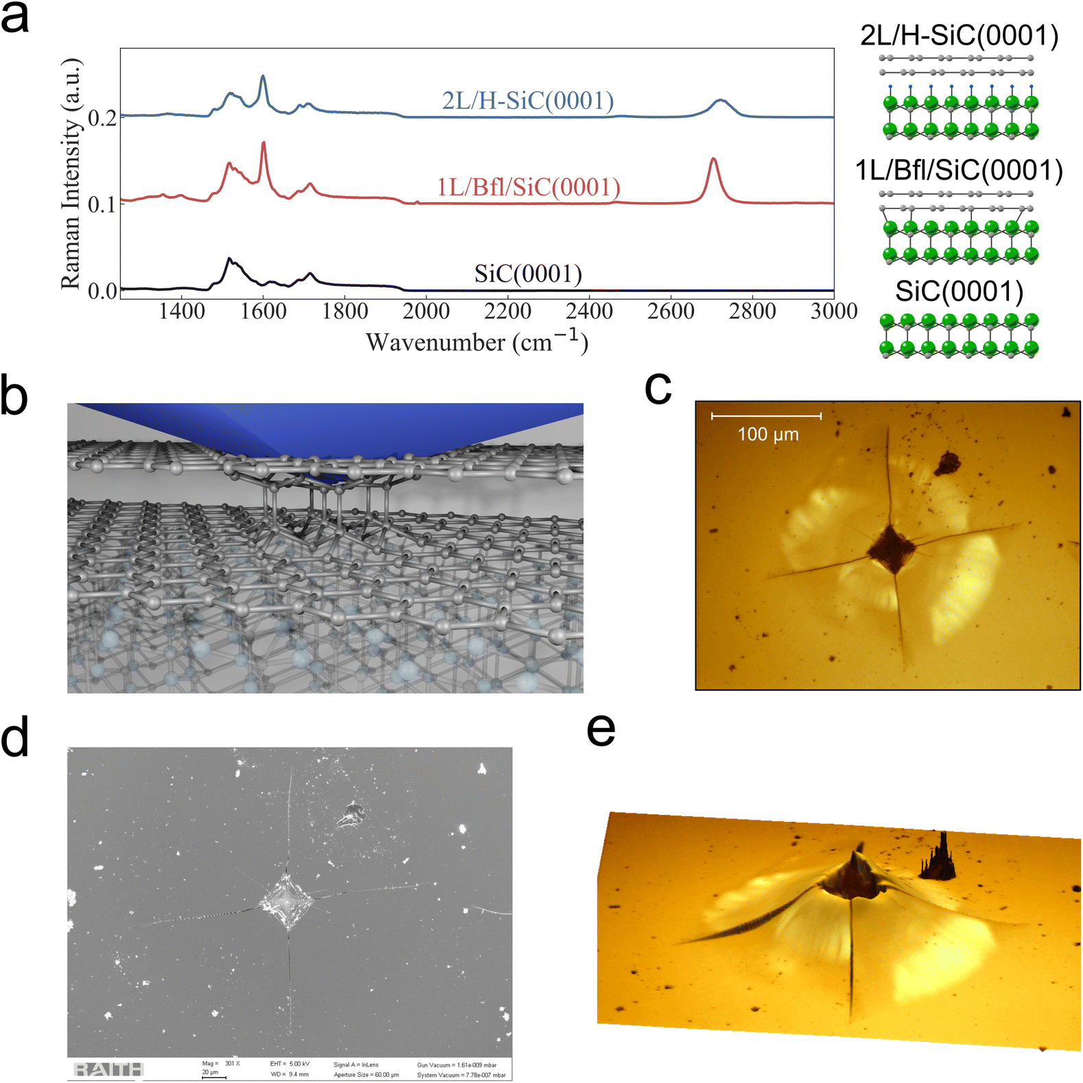 | ||
| Fig. 1 Hardness experiment. (a) Raman spectra of bare and graphene-coated SiC. The spectra are vertically shifted for clarity. On the right panel, from bottom to top, graphical schemes of bare silicon carbide, one epitaxial graphene layer on carbon buffer layer on the silicon face of SiC, and quasi-free-standing bilayer graphene on the hydrogenated silicon face of SiC. (b) Graphical scheme of the hardness experiments with a diamond Vickers indenter. The scheme shows the formation of the phase transformed diamene phase under the indenter. (c) Representative optical image of a residual indentation in 1L/BfL/SiC after indenting with a load of 30 N. (d) SEM and (e) 3D optical profilometer image of the residual indentation in c. | ||
Experimental procedure
Graphene coatings preparation
Epitaxial graphene films are grown on the Si-face of on-axis 6H SiC (SiC(0001)) crystal by the thermal decomposition method in an argon atmosphere.27 The first carbon layer on the Si-face of SiC contains approximately 30% of carbon atoms in the sp3 configuration.28 This layer is named the buffer layer (Bfl). Pure sp2 graphene layers are then grown on top of this buffer layer, and when we refer to two-layer epitaxial graphene, we intend to indicate one layer of pure sp2 graphene layers on top of the buffer layer, respectively.Hydrogen intercalation is used to prepare quasi-free-standing bilayer graphene (2L/H-SiC(0001)) from the two-layer epitaxial graphene sample (1L/Bfl/SiC(0001)) by breaking the sp3 bonds between the buffer layer and the SiC surface and creating Si–H bonds. More details about the hydrogen intercalation can be found in ref. 29 and 30.
The measured Raman spectra for each sample are depicted in Fig. 1a. The characteristic spectrum of SiC is shown as a black curve, while the spectrum of the 1L/Bfl/SiC(0001) sample is plotted in red, and the spectrum of the 2L/H-SiC(0001) sample is plotted in blue. The Raman spectrum of graphene-coated SiC consists of a D band (∼1350 cm−1), a G band (∼1580 cm−1), and a 2D band (∼2700 cm−1).31 The number of layers can be obtained from the full width at half maximum (FWHM) of the 2D peak and from the ratio of the integrated area of the 2D and G peaks.32 We find a FWHM of 29 cm−1 and a ratio of 2.36 for 1L/Bfl/SiC(0001), which is in agreement with literature values of 1L epitaxial graphene on buffer layer.27,33 For 2L/H-SiC(0001), we obtain a FWHM of 50 cm−1 and a ratio of 1.69, which is also in good agreement with literature values for 2L epitaxial graphene on buffer layer.29 Furthermore, the graphical side views of the investigated coating structures are depicted in Fig. 1a.
Hardness test
The graphene-coated and bare SiC samples are indented using a Qness Q10A automatic microhardness tester (Golling, Austria) with a Vickers diamond indenter (see graphical scheme in Fig. 1b) using different loads, between 0.5 N and 30 N, and with a dwell time of 10 s. The produced residual indentations on the sample surface are investigated and imaged by two different optical microscopes (OM) (see Fig. 1c), a scanning electron microscope (SEM) (see Fig. 1d), and a 3D optical surface profilometer (see Fig. 1e). The first optical microscope is a Nikon Eclipse LV150N optical microscope with a Nikon TU Plan Fluor objective (100× magnification and numerical aperture 0.9), and the second one is a WITec optical microscope with different objectives, namely Zeiss EC Epiplan 20×/0.4 (Magnification/NA), Zeiss LD EC Epiplan-Neofluar Dic 50×/0.55, and Zeiss EC Epiplan-Neofluar Dic 100×/0.9. A NewView 5000 3D optical surface profilometer from ZYGO with a 20× Mirau objective is used to measure the topography of indented samples. SEM measurements are performed with a Raith 150 Two electron beam metrology system with Carl-Zeiss Gemini electron optics. The aperture size is set at 60 μm and the voltage is 10 kV. A gold layer of 3 nm is evaporated on the sample surface to avoid sample charging during the SEM measurements.Hardness and fracture toughness evaluation
The hardness of the different coated and bare SiC samples is calculated according to the following equation | (1) |
 | (2) |
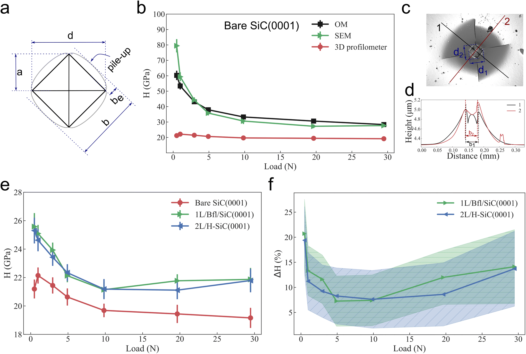 | ||
| Fig. 2 Hardness evaluation. (a) A schematic illustration of the residual indentation with produced pile-up (black dashed line) with labeled features used to determine the hardness H, a is the indentation size, d is the diagonal length, be corresponds to the semi-minor axis of the ellipse, and b is the maximal distance between two opposite highest points on pile-up. (b) The hardness of bare SiC substrate as a function of the maximal load estimated from measurements done by optical microscope (OM), SEM, and 3D profilometer. (c) Topography of the bare SiC substrate after indentation experiment, showing the produced residual indentation measured by a 3D optical profilometer. Two diagonal lengths d1 and d2 are shown as blue line segments, while solid black and red lines correspond to cross-section profiles depicted in d. (c) The hardness of graphene-coated SiC samples and bare SiC substrate as a function of maximal load. The hardness is calculated from 3D optical profilometer measurements using the eqn (8). The error bars correspond to the confidence level of 99%. (f) Calculated relative change in hardness of graphene-coated SiC compared to a bare SiC. | ||
Then the hardness is given by the following equation
 | (3) |
The fracture toughness KC is determined from the total length of the radial cracks from the indentation center to the end of crack c (see schematic illustration in Fig. 3a) using the following Lawn and Swain equation developed for radial-median ‘halfpenny’ shaped cracks34–36
 | (4) |
 | ||
| Fig. 3 Fracture toughness evaluation. (a) A schematic illustration of the residual indentation with labeled features used to determine the fracture toughness, a is the indentation size, the crack length at the surface is labeled as l, c corresponds to the sum of both previous quantities and d is the diagonal length. (b–e) Representative images of the residual indentations and produced cracks on bare SiC after indentation experiments at 0.5 N, 1 N, 3 N, and 10 N, respectively. (f) The calculated fracture toughness using eqn (4) as a function of the applied maximal load. (g) The relative change in fracture toughness of graphene-coated SiC compared to a bare SiC. | ||
Here a is the indentation half-diagonal length, while the constant W is equal to
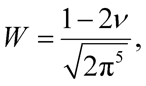 | (5) |
Results and discussion
Hardness
We estimate the hardness of a bare SiC using the eqn (3) and we plot the results in Fig. 2b as a function of the maximal applied load, where black squares represent hardness obtained from measurements of diagonal lengths d (in eqn (3)) made by OM, while the green triangles represent SEM measurements. The plotted results are obtained from an average of more than 20 measurements, and as can be seen, the data points from both methods overlap within the error. However, the SEM measurements lead to higher hardness values than OM measurements at small maximal loads. This is because of the higher lateral resolution of SEM compared to OM. Higher resolution of SEM allows better estimation of the diagonal length, which is especially crucial for residual indentations produced at low loads, when the diagonal length is around 4 μm. Overall, from both methods, the estimated hardness of a bare SiC is not constant and decreases with increasing load (see Fig. 2d), which is caused by neglecting pile-up formation around the indenter. This leads to an underestimation of the contact area resulting in an overestimation of the hardness.To overcome this issue, a 3D optical surface profilometer is used to measure changes in topography (see Fig. 2c), which allows us to detect a pile-up formation (see cross-sectional profiles in Fig. 2d). When pile-up occurs, usage of eqn (3) overestimates the hardness as a result of plastically piled-up material around the indenter. To obtain accurate results, the area must be estimated from topographic images (see Fig. 1e), and the pile-up formation must be considered. A schematic diagram of a square projection of the Vickers indenter (solid black lines) with a projection of the highest pile-up height (dashed black line) is drawn in Fig. 2a. Here, we assume that the material is mostly radially displaced at the center of the residual indentation edge, while no radial displacement occurs at the indentation corner. The distance between the highest points from the opposite pile-ups on the perpendicular curve to the edges and passing through the center of the indentation is defined as b. The distance between the residual indentation edge, and the maximal height of the pile-up is defined as be, which corresponds to the semi-minor axis of the ellipse. Then, the A consists of two elements, an area of the square indentation without pile-up AS and an area of four half ellipses AE. The half ellipse is defined by the edge of the square indentation and pile-up which creates the ellipse arc. The first element AS can be calculated without pile-ups from the eqn (2). The second component AE adds the contact area of the formed pile-up. From the previous assumption that the shape of the pile-up is elliptic, we can derive the following equation
 | (6) |
Then the contact area A is
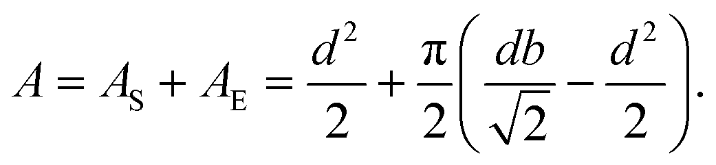 | (7) |
By combining eqn (1) and (7), the corrected hardness is given by
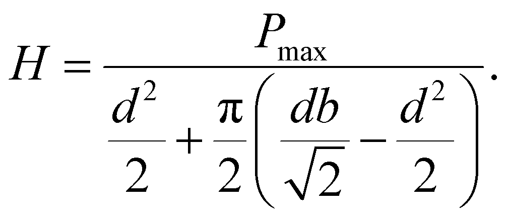 | (8) |
The corrected hardness of a bare SiC is calculated using eqn (8) and plotted as red circles in Fig. 2b. The corrected data show lower hardness values compared to the OM and SEM measurements. Furthermore, the hardness still decreases with increasing load (see Fig. 2e), probably due to the indentation size effect10,37,38 and/or approximation in the determination of the contact area. The asymptotic hardness of a bare SiC(0001) is around 19 GPa, which is consistent with the values reported in the literature (20–30 GPa (ref. 6 and 8–11)).
In Fig. 2e, we also report the measured hardness of graphene-coated SiC samples together with the bare SiC results. The results are obtained from measurements made by a 3D optical surface profilometer, and the hardness is calculated using the eqn (8). The figure clearly shows higher hardness values for graphene-coated SiC, namely 1L/Bfl/SiC(0001) (green triangles) and 2L/H-SiC(0001) (blue triangles), in the whole range of investigated loads, while the trend of the load dependency remains the same. To characterize the increase in hardness of graphene coated SiC compared to a bare SiC, we plot a relative change of hardness defined as
 | (9) |
Recently, a similar increase in the hardness of graphene-coated SiC, between 100% and 30%, has been reported for lower loads from 500 μN to 10 mN,17 which has been explained by the local formation of the diamene structure.20,22 Diamene is a diamond structure emerging from a pressure activated sp2 to sp3 phase transition in the two layers of graphene.20,22 Another source of the increased hardness can be attributed to the high in-plane stiffness of graphene of 1 TPa,24 that holds the hexagonal graphene network together at the boundaries of the impacted area. Here, we show that epitaxial graphene, which is only a few angstroms thick, can increase the hardness of SiC even for maximal indentation depths of 10 μm. The maximal indentation depth is calculated based on the indenter geometry and the measured average diagonal length. Interestingly, the depth of the indentation is approximately sixteen thousand times the thickness of the graphene coating, which is 5.7 Å.
Fracture toughness
We investigate the fracture toughness KC of a bare SiC substrate and graphene-coated SiC substrates. To compute the fracture toughness, we use the Lawn and Swain equation35 (eqn (4)) describing the halfpenny-shaped cracks, which are developed in the case of SiC in the range of investigated loads.13,39 We examine the dimensions of the cracks by means of an OM. Fig. 3a shows the labelled characteristics used to estimate the fracture toughness. The measured OM images of the residual indentations for maximal loads of 0.5 N, 1 N, 3 N, and 10 N are shown in Fig. 3b–e, where the development of cracks with increasing load is visible. Firstly, the lateral cracks are seen as halos around the residual indentations. While the halos create full circles for indentations from 1 N and higher loads, the halo is not fully developed around the residual indentation at 0.5 N. Secondly, radial cracks are formed at the corners of the residual indentations. Six cracks are developed for loads 0.5 N (Fig. 3b) and 1 N (Fig. 3c), respectively. The angle between cracks is around 60°, which most probably corresponds to an atomic arrangement of 6H polytype of SiC in (0001) direction. For higher loads, four main cracks are visible with an angle of 90° between them. Moreover, minor cracks are visible in different directions resembling formed cracks for lower loads.In Fig. 3f, we show the evolution of fracture toughness with load for a bare SiC and graphene-coated SiC samples. The fracture toughness of a bare SiC sample varies between 1.3 and 1.4 MPa m1/2 with an average value 1.36 MPa m1/2, which is in agreement with the previously reported values.8,9,13,14 For 1L/Bfl/SiC(0001) and 2L/H-SiC(0001) the fracture toughness values are above the values of a bare SiC (see Fig. 3f), and the mean fracture toughness is 1.52 MPa m1/2 and 1.49 MPa m1/2, respectively. The relative change of fracture toughness compared to a bare SiC in dependency on load is depicted in Fig. 3g, showing an increase of 12% for 1L/Bfl/SiC(0001) and 10% for 2L/H-SiC(0001). The results therefore demonstrate that two-layer thick graphene coating can produce a concurrent increase of hardness and toughness in SiC. This result is very surprising since increase in hardness in a material is usually accompanied by a decrease in toughness. The results can be explained considering the graphene-diamene phase transition occurring under the indenter17,22 while the rest of the coating remains in the ultra-tough graphene phase.24–26
Conclusions
In conclusion, we find that atomically thin graphene coatings can improve the hardness of SiC crystals even for large loads in the range 0.5 N to 30 N, corresponding to indentation depths up to ∼10 μm, approximately sixteen thousand times the thickness of the graphene coating. Interestingly, the graphene coating causes an increase of the fracture toughness by 11% compared to bare SiC. These results, which do not follow the general indirect relationship between the hardness and the fracture toughness can be attributed to the graphene diamene local transition under the indenter. This research opens new venues for understanding hardness and toughness in materials undergoing local phase transitions and new possibilities for graphene-coated SiC applications in aeronautics, aerospace, automotive industry, body armor production, and high-impact protective coatings.Author contributions
M. R., V. D. and E. R. conceived and designed the experiments. M. S. and J. K. prepared and characterized the samples. M. R and V. D. performed the microindentation experiments. M. R. and J. K. carried out the measurements of the residual indentations on the surface of studied samples and analysed the data. E. R. supervised research and data analysis. M. R. wrote the manuscript, with contributions from all authors.Conflicts of interest
The authors declare no conflicts of interest.Acknowledgements
This work was supported by the US Army Research Office under Award # W911NF2020116 and the U.S. Department of Energy, Office of Science, Basic Energy Sciences, MSE Division under Award # DE-SC0018924. The authors would like to thank M. Čepová for assistance with the indentation experiment, and acknowledges the CzechNanoLab Research Infrastructure supported by MEYS CR (LM2023051).References
- P. G. Neudeck and G. K. Sujan, Silicon Carbide Electronic Devices, in Reference Module in Materials Science and Materials Engineering, Elsevier, 2016 Search PubMed.
- T. X. Xu, et al., Effect of thermal annealing on the defects and electrical properties of semi-insulating 6H-SiC, J. Cryst. Growth, 2020, 531, 125399 CrossRef CAS.
- N. D. Shcherban, Review on synthesis, structure, physical and chemical properties and functional characteristics of porous silicon carbide, J. Ind. Eng. Chem., 2017, 50, 15–28 CrossRef CAS.
- J. A. Xu and H. K. Mao, Moissanite: A window for high-pressure experiments, Science, 2000, 290(5492), 783–785 CrossRef CAS PubMed.
- J. A. Xu, et al., The moissanite anvil cell: a new tool for high-pressure research, J. Phys.: Condens.Matter, 2002, 14(44), 11543–11548 CrossRef CAS.
- P. Chai, et al., Mechanical Behavior Investigation of 4H-SiC Single Crystal at the Micro–Nano Scale, Micromachines, 2020, 11(1), 102 CrossRef PubMed.
- A. Datye, U. Schwarz and H.-T. Lin, Fracture Toughness Evaluation and Plastic Behavior Law of a Single Crystal Silicon Carbide by Nanoindentation, Ceramics, 2018, 1(1), 198–210 CrossRef CAS.
- J. L. Henshall and C. A. Brookes, The measurement of KIC in single crystal SiC using the indentation method, J. Mater. Sci. Lett., 1985, 4(6), 783–786 CrossRef CAS.
- J. L. Henshall, D. J. Rowcliffe and J. W. Edington, Fracture Toughness of Single-Crystal Silicon-Carbide, J. Am. Ceram. Soc., 1977, 60(7–8), 373–374 CrossRef CAS.
- J. Qian, L. L. Daemen and Y. Zhao, Hardness and fracture toughness of moissanite, Diamond Relat. Mater., 2005, 14(10), 1669–1672 CrossRef CAS.
- P. T. B. Shaffer, Effect of Crystal Orientation on Hardness of Silicon Carbide, J. Am. Ceram. Soc., 1964, 47(9), 466–466 CrossRef CAS.
- M. Kuhn, D. Tierney and M. Simmers, Silicon carbide for the modern warfighter, Am. Ceram. Soc. Bull., 2017, 96(8), 38–39 CAS.
- N. Cuadrado, et al., Geometry of nanoindentation cube-corner cracks observed by FIB tomography: Implication for fracture resistance estimation, J. Eur. Ceram. Soc., 2015, 35(10), 2949–2955 CrossRef CAS.
- K. M. Liang, G. Orange and G. Fantozzi, Evaluation by Indentation of Fracture-Toughness of Ceramic Materials, J. Mater. Sci., 1990, 25(1a), 207–214 CrossRef CAS.
- D. Ray, et al., Hardness/toughness relationship for SiC armor, 27th International Cocoa Beach Conference on Advanced Ceramics and Composites: A, 2003, 24(3), 401–410.
- D. Ray, et al., Effect of Room-Temperature Hardness and Toughness on the Ballistic Performance of SiC-Based Ceramics, in Advances in Ceramic Armor: A Collection of Papers Presented at the 29th International Conference on Advanced Ceramics and Composites, January 23–28, 2005, Cocoa Beach, Florida, Ceramic Engineering and Science Proceedings, 2005, 131–142.
- M. Rejhon, et al., Giant Increase of Hardness in Silicon Carbide by Metastable Single Layer Diamond-Like Coating, Adv. Sci., 2023, 10(6), 2204562 CrossRef CAS PubMed.
- F. Cellini, Y. Gao and E. Riedo, Å-Indentation for non-destructive elastic moduli measurements of supported ultra-hard ultra-thin films and nanostructures, Sci. Rep., 2019, 9(1), 4075 CrossRef PubMed.
- F. Cellini, et al., Layer dependence of graphene-diamene phase transition in epitaxial and exfoliated few-layer graphene using machine learning, 2D Mater., 2019, 6(3), 035043 CrossRef CAS.
- F. Cellini, et al., Epitaxial two-layer graphene under pressure: Diamene stiffer than Diamond, FlatChem, 2018, 10, 8–13 CrossRef CAS.
- F. Cellini, et al., Pressure–Induced Formation and Mechanical Properties of 2D Diamond Boron Nitride, Adv. Sci., 2020, 2002541 Search PubMed.
- Y. Gao, et al., Ultrahard carbon film from epitaxial two-layer graphene, Nat. Nanotechnol., 2018, 13(2), 133–138 CrossRef CAS PubMed.
- F. Lavini, M. Rejhon and E. Riedo, Two-dimensional diamonds from sp2-to-sp3 phase transitions, Nat. Rev. Mater., 2022, 7(10), 814–832 CrossRef.
- C. Lee, et al., Measurement of the elastic properties and intrinsic strength of monolayer graphene, Science, 2008, 321(5887), 385–388 CrossRef CAS PubMed.
- M. U. Arshad, et al., Fracture Toughness Characteristics of Stacked Bilayer Graphene via Far-Field Displacement Measurements, Small, 2023, 19(39), 2302499 CrossRef CAS PubMed.
- B. Jang, et al., Uniaxial fracture test of freestanding pristine graphene using tensile tester under scanning electron microscope, Extreme Mech. Lett., 2017, 14(.), 10–15 CrossRef.
- J. Kunc, et al., Effect of Residual Gas Composition on Epitaxial Growth of Graphene on SiC, Phys. Rev. Appl., 2017, 8(4), 044011 CrossRef.
- K. V. Emtsev, et al., Interaction, growth, and ordering of epitaxial graphene on SiC{0001} surfaces: A comparative photoelectron spectroscopy study, Phys. Rev. B: Condens. Matter Mater. Phys., 2008, 77(15), 155303 CrossRef.
- J. Kunc, M. Rejhon and P. Hlidek, Hydrogen intercalation of epitaxial graphene and buffer layer probed by mid-infrared absorption and Raman spectroscopy, AIP Adv., 2018, 8(4), 045015 CrossRef.
- M. Rejhon and J. Kunc, ZO phonon of a buffer layer and Raman mapping of hydrogenated buffer on SiC(0001), J. Raman Spectrosc., 2018, 50(3), 465–473 CrossRef.
- M. Paillet, et al., Graphene and related 2D materials: An overview of the Raman studies, J. Raman Spectrosc., 2018, 49(1), 8–12 CrossRef CAS.
- J. S. Hwang, et al., Imaging layer number and stacking order through formulating Raman fingerprints obtained from hexagonal single crystals of few layer graphene, Nanotechnology, 2013, 24(1), 015702 CrossRef PubMed.
- D. S. Lee, et al., Raman Spectra of Epitaxial Graphene on SiC and of Epitaxial Graphene Transferred to SiO, Nano Lett., 2008, 8(12), 4320–4325 CrossRef CAS PubMed.
- Y. Guo, et al., A detailed analysis of the determination of fracture toughness by nanoindentation induced radial cracks, J. Eur. Ceram. Soc., 2020, 40(2), 276–289 CrossRef CAS.
- C. B. Ponton and R. D. Rawlings, Vickers Indentation Fracture-Toughness Test.1. Review of Literature and Formulation of Standardized Indentation Toughness Equations, Mater. Sci. Technol., 1989, 5(9), 865–872 CrossRef.
- M. V. Swain and B. R. Lawn, Indentation Fracture in Brittle Rocks and Glasses, Int. J. Rock Mech. Min. Sci., 1976, 13(11), 311–319 CrossRef.
- T. F. Page, W. C. Oliver and C. J. Mchargue, The Deformation-Behavior of Ceramic Crystals Subjected to Very Low Load (Nano)Indentations, J. Mater. Res., 1992, 7(2), 450–473 CrossRef CAS.
- J. B. Quinn and G. D. Quinn, Indentation brittleness of ceramics: A fresh approach, J. Mater. Sci., 1997, 32(16), 4331–4346 CrossRef CAS.
- G. D. Quinn, et al., Fracture origins in miniature silicon carbide structures, in Key Engineering Materials, 2005, vol. 290, pp. 62–69 Search PubMed.
| This journal is © The Royal Society of Chemistry 2024 |