
 Open Access Article
 This Open Access Article is licensed under a Creative Commons Attribution-Non Commercial 3.0 Unported Licence
Enhanced linear and symmetric synaptic weight update characteristics in a Pt/p-LiCoOx/p-NiO/Pt memristor through interface energy barrier modulation by Li ion redistribution
Boyoung
Jeong
a,
Peter Hayoung
Chung
a,
Jimin
Han
b,
Taeyun
Noh
a and
Tae-Sik
Yoon
 *ab
*ab
aGraduate School of Semiconductor Materials and Devices Engineering, Ulsan National Institute of Science and Technology, Ulsan 44919, Republic of Korea. E-mail: tsyoon@unist.ac.kr
bDepartment of Materials Science and Engineering, Ulsan National Institute of Science and Technology, Ulsan 44919, Republic of Korea
First published on 27th February 2024
Abstract
Artificial synaptic devices have been extensively investigated for neuromorphic computing systems, which require synaptic behaviors mimicking the biological ones. In particular, a highly linear and symmetric weight update with a conductance (or resistance) change for potentiation and depression operation is one of the essential requirements for energy-efficient neuromorphic computing; however, it is not sufficiently met. In this study, a memristor with a Pt/p-LiCoOx/p-NiO/Pt structure is investigated, where a low interface energy barrier between the Pt electrode and the NiO layer makes for a more linear and symmetric conductance change. In addition, the use of voltage-driven Li+ ion redistribution in the NiO layer facilitates the analog conductance change at a low voltage. Besides the linear and symmetric potentiation and depression weight updates, the memristor exhibits various synaptic characteristics such as the dependence of weight update on the pulse amplitude and number, paired pulse facilitation, and short-term and long-term plasticity. The conductance modulation is thought to be induced by a tunable interface energy barrier at the NiO layer and Pt bottom electrode, as a result of Li+ ion diffusion in NiO supplied from the LiCoOx layer and their redistribution. Thanks to the use of Li+ ion redistribution, the conductance change could be achieved at a voltage <4 V within the time of μs range. These results verify the potential of artificial synapses with the Pt/LiCoOx/NiO/Pt memristor operated by voltage-driven Li+ ion redistribution under the low interface energy barrier conditions, realizing a highly linear and symmetric weight update at a low voltage with a high speed for energy-efficient neuromorphic computing systems.
1. Introduction
In the current big data era, silicon CMOS-based computing systems face challenges due to their limited device scaling and accompanying technology development. In addition, the performance gap expanding between memory and processor as well as physical separation between memory and processor (known as “memory wall” problem) causing the von Neumann bottleneck make the current computing hardware and architectures inefficient for data-intensive computing like artificial intelligence.1 In this point of view, the needs to develop new computing hardware and architectures keep increasing. Neuromorphic computing is considered to be one of the emerging new computing architectures to efficiently deal with a vast amount of data, overcoming the technology limit of the von-Neumann computing architecture. This new computing architecture mimics the human brain that is made up of extremely dense neural networks composed of ∼ 1011 neurons for the computing element and ∼1015 synapses for the memory element. These neurons and synapses forming a highly complex network in the human brain conduct complicated cognitive tasks such as pattern recognition and calculation with a low energy consumption of ∼20 W.2,3 Neuromorphic computing systems aim to mimic the human brain by constructing a parallel, three-dimensional, and compact neuron-synapse network in hardware and processing the data in a parallel way at the architectural level.4In the neuromorphic system, artificial neuron and synaptic devices should be developed to operate their functions and integrated together to mitigate the delay in data transfer as opposed to the current von Neumann architecture. The artificial synaptic device as one of the essential elements should conduct the processing of signals coming from pre-neurons and deliver it to post-neurons in association with its synaptic weight. At the same time, the synapse should store the weight information that is updated as a result of signal processing. Therefore, an artificial synaptic device needs to be developed to have tunable conductance corresponding to synaptic weight, which is stored as updated weight through a process known as synaptic plasticity for the learning process of the human brain.5 Synaptic weight represents the connection strength between neurons that could be strengthened for potentiation and weakened for depression.6 For a more efficient computing operation, the synaptic weight update is pursued to be analog, linear, and symmetric and to have a wide dynamic range to enhance the range of memory states.7,8
Among various candidate devices for artificial synapses, two-terminal memristors have been extensively explored due to their advantage of having a similar structure to the biological neuron-synapse-neuron structure. Memristors exhibit tunable conductance states depending on historical electrical signals emulating the dynamic synaptic weight update behavior. If the weight-tunable conductance change could be achieved in an analog manner, it would enable to store multibit (or analog) state information rather than storing digital-type information in the binary state of 0 and 1.9 As among the two-terminal memristor devices, resistive random access memory devices (RRAM), including conductive bridge random access memory (CBRAM) using a metallic filament, valence change memory (VCM) with an oxygen-vacancy filament, and interfacial-type RRAM with oxygen redistribution particularly at the interface, have been reported to have low energy consumption down to sub-pJ per synaptic event and good scalability for high-density integration, forming a crossbar array structure with CMOS compatibility.10–12
To date, RRAM devices with a variety of oxides have been researched for synaptic device application, such as HfO2,13–15 Ta2O3,16–18 WOx,19–21 TiO2,22–24 CeO2,7,25,26 ZnO,27–29 NiO,30–32 SrFeOx,33 and PCMO.34,35 With respect to the resistance change mechanism, filamentary-type CBRAM and VCM suffer from a non-linear, digital-type and asymmetric resistance change with a large device-to-device variation due to the abrupt and stochastic nature of filament formation.5,36 In comparison, interfacial-type RRAM with the resistance change associated with ion redistribution is thought to be more promising to achieve a precise and gradual resistance change in an analog manner as well as resulting in various biological synaptic behaviors such as short-term and long-term plasticity (STP and LTP), and paired pulse facilitation or depression (PPF and PPD). In order to achieve more reliable control of ionic redistribution, bilayer structures were also employed such as GDC/CeO2,7 WOx/TaOx,37 TiO2/Al2O3,38 AlOx/HfO2,39 HfO2/Al2O3,40 TaOx/TiO2,41 HfO2/HfO2−x,42 and HfOy/HfOx.43
Particularly, for linear and symmetric weight update, the identical incremental change of conductance should be achieved in each conductance state. However, because the conductance is dependent on the interface energy barrier such as the Schottky barrier in many devices, it varies exponentially with respect to the change of the energy barrier. Thus, it is hard to control this barrier to realize a linear conductance change. As a result, the conductance is generally found to be more abruptly changed at the initial stage of high resistance and decrease as the resistance decreases, resulting in a non-linear and asymmetric conductance change. This occurs more apparently in the system with a high interface energy barrier when the oxides are n-type and metal electrodes have a high work function (e.g. Pt).
In that sense, it is preferred to employ metal oxide and electrode materials that have a low interfacial energy barrier that could prevent an abrupt conductance change and provide a precisely tunable barrier by ion redistribution within the layers. For this, if a p-type oxide is used instead of an n-type oxide, a lower interface barrier would be formed with a high work function metal electrode (e.g. Pt); therefore, the current changes in an analog manner with a good linearity. Although it brings out a concern of a large current flow due to a low Schottky barrier, it could be mitigated by scaling down the device size because the current of the interfacial-type memristor is proportional to the device size.
In this study, a memristor consisting of p-type LiCoOx and p-type NiO bilayer structures with a Pt electrode, i.e., Pt/p-LiCoOx/p-NiO/Pt, is proposed as an artificial synapse and its synaptic behaviors are investigated. LiCoOx is actively used as the cathode material in Li-ion batteries. It exhibits p-type oxide characteristics which are associated with the presence of trace amounts of Co4+ ions.44 It has a layered structure and Li+ ions exist between the layers composed of cobalt oxides. Due to the weak van der Waals force between cobalt oxides, Li+ ions can migrate easily with a high ionic diffusivity.45,46 NiO is also a p-type oxide with a band gap energy of about 3.6–4.0 eV.47,48 It has been researched for various applications, such as gas sensors,49 perovskite light emitting diodes,50 electrochromic displays51 and RRAM devices.52 Its p-type characteristics come from the presence of Ni vacancies and the resulting Ni3+ ions.53 Herein, it is expected that a thin LiCoOx layer supplies Li+ ions to the NiO layer, and their redistribution would consequently change the interfacial energy barrier and conductance state. The use of Li+ ions to modulate the conductance for artificial synapse has been explored in many studies because the Li+ ion works as a dopant in many oxides and easily redistributes, thanks to its low mass. For example, Zhang et al. reported a memristor with porous MoS2 nanosheets and a porous SiOx structure operated by the formation of conductive paths for Li+ ions enabling multilevel-ion dynamics.54 Kim et al. reported a Li-based memristor where the resistance changed with the relative fraction of Li7Ti5O12 as a metallic phase and Li4Ti5O12 as an insulating phase.55 Meng et al. proposed a Li+-doped organic artificial memristor that exhibited a gradual resistance change with multi-state storage using Li doped PEDOT:PSS.56 Despite the advantage of using Li+ ions for low voltage and high speed operation, there is a reliability concern due to its poor CMOS compatibility.57 However, this concern could be addressed by appropriate engineering of passivating the device and integrating devices in the back-end of line (BEOL) of the system.
2. Experimental
The Pt/LiCoOx/NiO/Pt memristors illustrated in the inset of Fig. 1(a) were fabricated as follows: first, a 70 nm-thick bottom Pt electrode (BE) was deposited on a SiO2/Si substrate with a 3 nm-thick Ti adhesion layer through e-beam evaporation (FC-2000, Temescal). Then, a 25 nm-thick NiO layer was deposited by radio-frequency (RF) magnetron sputtering using a NiO target in Ar. Next, a 10 nm-thick LiCoOx layer was deposited on the NiO layer by RF magnetron sputtering using a LiCoOx target in Ar. Subsequently, a 70 nm-thick Pt top electrode (TE) was deposited by e-beam evaporation using a shadow mask with a diameter of 100 μm. Finally, the device was passivated with a SiO2 layer deposited by RF magnetron sputtering with a thickness of about 50 nm to protect the device from being exposed to the atmosphere. | ||
| Fig. 1 (a) and (b) Cross-sectional high-resolution TEM images, schematic illustration, and optical microscopy image of the Pt/LiCoOx/NiO/Pt memristor, (c) its SADP, (d) its compositional EDS line scan and (e) elemental mapping data. | ||
For the electrical characteristic assessments of the device, current–voltage (I–V) curves were obtained by a DC voltage sweep using an Agilent 4156B semiconductor parameter analyzer. In addition to I–V characteristics, the conductance change characteristics as synaptic behaviors by successive pulse application were evaluated using Agilent 4156B and Keithley 4200A-SCS semiconductor parameter analyzers. The structural and composition analyses were conducted using transmission electron microscopy (TEM; JEM-2100F, JEOL) combined with energy-dispersive spectroscopy (EDS). The chemical compositional distribution was examined by time-of-flight secondary ion mass spectroscopy (TOF-SIMS; TOF.SIMS 5, ION TOF). CrossSim Ver. 2.0 Training was used for benchmarking the pattern recognition performance of the fabricated synapic device.58 At the algorithm level, the neural network consists of 3 layers, 784 input neurons, 300 hidden neurons, and 10 output neurons. Random initial weights were used for the run. Sigmoid function was used for the first and second layers and Softmax function was used for the last layer. The circuit level noise was neglected for better comparison of the device performances. For the learning rate, a default value of simulation was used. For training and testing, the Modified National Institute of Standards and Technology (MNIST) data set was used.59 For each epoch, 60![[thin space (1/6-em)]](https://www.rsc.org/images/entities/char_2009.gif) 000 images were used for training and the pattern recognition accuracy was tested with 10000 images.
000 images were used for training and the pattern recognition accuracy was tested with 10000 images.
3. Results and discussion
The cross-sectional high-resolution TEM (HRTEM) images in Fig. 1(a) and (b) show the stacked structure of Pt TE, LiCoOx, NiO, and Pt BE layers. The relatively bright part near the Pt TE presents a thin polycrystalline LiCoOx layer. The NiO layer under LiCoOx is also confirmed to be polycrystalline. The enlarged image in Fig. 1(b) confirms a relatively rough and unclear interface between NiO and LiCoOx layers, which is thought to come from either the polycrystalline structure of the underlying NiO layer with a rough surface or intermixing during deposition as a result of fast Li+ ion diffusion. Fig. 1(c) shows the selected area diffraction patterns (SADPs) of Pt, LiCoOx, and NiO layers. The polycrystalline LiCoOx, NiO and Pt layers were verified from the SADP results. These patterns matched well with rhombohedral LiCoO2 (JCPDS 50-0653), cubic NiO (JCPDS 89-7130) and the Pt electrode. The compositional EDS line scan and elemental mapping data are shown in Fig. 1(d) and (e). The LiCoOx layer can be clearly distinguished from the NiO layer with the Co signal from the LiCoOx layer.TOF-SIMS analysis was conducted for more accurate detection of Li+ ions, which is crucial for the conductance of the Pt/LiCoOx/NiO/Pt memristor. The analysis was processed in negative mode by sputtering Cs+ ions. Fig. 2 shows the atomic spectra in the pristine state of the Pt/LiCoOx/NiO/Pt memristor. The SiO2 capping layer, Pt TE, LiCoOx, NiO, and Pt BE layers were confirmed using the spectra. In Li− spectra, it is notable that the Li atoms or ions are present inside the NiO layer even in the pristine state before applying the bias. It verifies that Li atoms or ions penetrated the NiO layer during LiCoOx deposition on NiO by the sputtering process. It coincides with the TEM analysis results where the boundary between LiCoOx and NiO layers is not clearly distinct. As will be discussed later, the infiltrated Li+ ions into the NiO layer relocate under an electric field and consequently change the conductance of the Pt/LiCoOx/NiO/Pt memristor. As the Li+ ion is a light and easily movable element under the bias, the incorporated Li+ ions in the NiO layer acting as dopants could modulate the interfacial energy barrier as being redistributed upon biasing. The detailed conductance change mechanism with respect to the profile of Li+ ions is discussed in Fig. 4.
 | ||
| Fig. 2 TOF-SIMS results of the Pt/LiCoOx/NiO/Pt memristor. | ||
Fig. 3(a) and (b) show the I–V curves of the Pt/LiCoOx/NiO/Pt memristor under the DC voltage sweeps, where positive voltage sweeps of 0∼+2 V in the double direction were applied repeatedly 5 times at first. Then, the same number of negative sweeps of 0∼–2 V in the double direction were repeated. In this measurement, the additional forming operation was not carried out. It clearly shows that the current increased sequentially in the clockwise direction in the negative voltage sweeps and reached over 10 times higher at −2 V after 25 times of consecutive sweeps. In contrast, the current was rarely changed in the positive voltage sweeps even with counterclockwise hysteresis. In following negative voltage sweeps after positive sweeps, the current increased again from almost initial level. It means that the positive sweeps restored the changed conductance mostly to the initial level. Though these I–V curves do not show the decrease of current in the positive voltage region, they confirm voltage polarity-dependent conductance changes measured under the negative voltage read condition, which mimics the synaptic weight modulation. As will be discussed later, this conductance change comes from Li+ ion redistribution within the NiO layer. Through Li+ ion migration, the NiO/Pt BE energy barrier gets modulated. Then, the conductance increased or decreased consequently according to the height of the energy barrier at NiO/Pt BE.
 | ||
| Fig. 3 I–V curves of the Pt/LiCoOx/NiO/Pt memristor upon repeating positive and negative DC voltage sweeps in the (a) and (b) −2 to +2 V range and (c) and (d) −3.5 to +3.5 V range. | ||
Fig. 3(c) and (d) show the I–V characteristics with the sweep voltage range increased to ±3.5 V. The same as Fig. 3(a) and (b), the current increased in the clockwise direction at the negative voltage sweeps while remained or slightly decreased at the positive voltage sweeps. The conductance change was enhanced as the voltage sweep amplitude increased from ±2.0 to ±3.5 V, corresponding to stronger synaptic stimuli.
Fig. 4(a) shows the conductance change of the Pt/LiCoOx/NiO/Pt memristor as log-scale plots in voltage pulse measurements. The pulses of −2 V for potentiation and +2 V for depression with a pulse width of 0.64 ms were applied consecutively 50 times for each operation. The read condition was set at −1 V of amplitude and 0.64 ms of width. The cycle was repeated 10 times. In all measurements, the current changed barely at the first depression pulses of +2 V (blue circles). Then, the current increased gradually in a linear form during successive negative pulses, which corresponds to potentiation (red circles). The current increased about 30 times from the initial value at the first potentiation cycle. In the following cycle of positive pulses, the current gradually decreased mimicking the depression behavior. A decrease in current starts at a current value little higher than the last current of potentiation, which is thought to be due to the charging effect present in the device. Though the conductance was not completely restored to its initial value, the range of conductance modulation through entire cycles of potentiation and depression was found to be uniform. It is also notable that the depression behavior is observed only after the potentiation operation. As explained in Fig. 5 for a detailed mechanism, the conductance modulation comes from the distribution of Li+ ions that penetrate from the LiCoOx layer upon biasing as well as introduced into the NiO layer in advance during the sputtering process.
 | ||
| Fig. 4 Potentiation and depression behaviors of the Pt/LiCoOx/NiO/Pt memristor by voltage pulse measurements: (a) and (b) conductance change upon repeating +2 and −2 V pulse application and read at −1 V on log and linear scales, respectively, (c) and (d) degree of potentiation and depression obtained from (e) the conductance change of 17 devices. | ||
 | ||
| Fig. 5 Schematic illustration of mechanisms with NiO/Pt(BE) interfacial energy band modulation: (a) initial state of the Pt/LiCoOx/NiO/Pt memristor, (b) potentiation by applying a −V to the TE and (c) depression by applying a +V to the TE. | ||
Fig. 4(b) is the linear plot of the conductance change shown in Fig. 4(a). The weight update both at potentiation and depression operation was found to be linear and symmetric during the repeated cycles up to 1000 times of pulse application. A highly linear and symmetrical weight update is one of the crucial factors required for accurate pattern recognition in the learning process.60 The pattern recognition simulation results with the presented synaptic weight update characteristics using the CrossSim simulator will be discussed later in Fig. 8.
The uniformity of conductance change is important for accurate weight update operation in the neural network. The device-to-device and cycle-to-cycle variations obtained from 17 devices are presented in Fig. 4(c) and (d) for the potentiation and depression operation, respectively. The repeated pulse measurement results from 17 devices used for this variation analysis are shown in Fig. 4(e). The degree of potentiation and depression was obtained by measuring the current ratio at the −1 V reading condition before and after the application of fifty times −2 V pulse and fifty times +2 V pulse, respectively. Also, the cycle-to-cycle variation was reflected from the values after five cycles of potentiation and four cycles of depression. In this evaluation, the first cycle of depression was excluded because the current changed barely at the first depression. The results show that the mean values (μ) of the degree of potentiation and depression are 8.3 and 6.8 with standard deviations (σ) of 2.8 and 1.7, respectively, corresponding to 34 and 25% distribution in potentiation and depression, respectively.
The conductance change mechanism in the Pt/LiCoOx/NiO/Pt memristor was proposed as shown in Fig. 5, based on the energy band of each layer, the analysis results of the presence of introduced Li+ ions in the NiO layer, plausible supply of Li+ ions from LiCoOx into NiO, and redistribution of Li+ ions within the NiO layer. In this mechanism, the role of Li+ ions in the NiO layer is a decisive factor for conductance change. Assuming that the Li+ ions act as dopants in NiO, two opposing conditions should be considered for the effect of Li+ ions on the doping state of the NiO layer. The first one is if Li+ ions filled Ni vacancies, the hole concentration generated from Ni vacancies would be reduced, thereby making NiO less p-type. The other is if Li+ ions substituted Ni2+ sites, more holes would be created, then the NiO layer would be more p-type consequently.
Therefore, the effect of Li doping on the doping state of the NiO layer would be determined competitively based on whether incorporated Li+ ions would make NiO more or less p-type depending on their occupation sites.61 In this Pt/LiCoOx/NiO/Pt memristor, the tendency of conductance change with respect to the bias polarity coincides well with that Li+ ions fill Ni vacancies to make NiO less p-type. Because the LiCoOx layer is found to be much thinner than the NiO layer from the TEM results, the overall conductance is assumed to be determined dominantly by the doping state of the NiO layer and the resulting interfacial energy barrier with Pt BE. Although not shown here, the current range increased proportionally to the electrode area, verifying that the conductance change is induced by the modulation at the interface. In addition, it is also considered that Li+ ions are already distributed in the NiO layer close to Pt BE according to TOF-SIMS results in Fig. 2.
As illustrated in Fig. 5(a), both LiCoOx and NiO layers are p-type doped and some amount of Li+ ions are already present in the NiO layer even before biasing. As negative voltage is applied to the Pt TE for potentiation, Li+ ions in the NiO layer assemble close to the Pt TE and are depleted near the Pt BE, making NiO near Pt BE more p-type. As a result, the energy barrier at the NiO/Pt(BE) interface is decreased. Consequently, the conductance measured at −V increased with increased hole charge transport, and potentiation behavior occurs as shown in Fig. 5(b). In contrast, when positive voltage is applied to Pt TE as shown in Fig. 5(c), Li+ ions are repelled from the Pt TE interface and assembled near at the interface with Pt BE. Then, the energy barrier at NiO/Pt(BE) increases, and consequently conductance is reduced as depression behavior at the −V read condition for hole charge transport (Fig. 5(c)).
This interpretation that Li+ ion redistribution in the NiO layer plays a decisive role in conductance modulation explains well the voltage-polarity dependence of conductance change. The linear weight modulation in the present device is attributed mostly to the device structure having a low interface energy barrier in the combination of high work function Pt BE and p-type NiO with inserted thinner p-LiCoOx. In addition, the gradual energy barrier modulation by the redistribution of fast movable Li+ ions in the NiO layer would facilitate the linear weight update without abrupt changes.
In addition, Pt/LiCoOx/NiO/Pt memristors exhibit various synaptic characteristics. As shown in Fig. 6(a), the time-dependent decay of synaptic weight (retention properties) for 10 minutes was examined with respect to the pulse amplitude after potentiation by applying 50 times of −2, −2.5, −3, and −3.5 V pulses with 0.64 ms of pulse width and then reading the current at −1 V of the read condition. After repeating −2 V pulse application, the current increased from an initial value of 6.84 to 78.7 nA, then decreased back to 6.55 nA after 10 minutes. The decay to almost initial value implies the STP characteristics of the memristor when the voltage pulse amplitude was low to be −2 V. As the potentiation pulse amplitude increased, the current increased higher and it was not completely restored but remained to be higher than the initial value as LTP characteristics. Under the condition of −3.5 V pulse amplitude, the current increased from 6.05 nA to 11.4 μA by about 2000 times. Then, it decayed to 0.21 μA, which is still 35 times higher than the initial state. The current levels for each amplitude could be sufficiently distinguishable even after decay, describing multi-state retention characteristics depending on the pulse amplitude. These time-dependent characteristics show the potential of the device to emulate the synaptic properties such as PPF, STP and LTP. However, even with the potential application of time-dependent characteristics, this decay of conductance over time frequently observed in the interface-type devices7,62 needs to be alleviated to achieve long-term reliability of weight storage.
 | ||
| Fig. 6 Synaptic properties of the Pt/LiCoOx/NiO/Pt memristor; retention results of (a) depending on the potentiation pulse amplitude and (b) number of pulse application, and (c) PPF characteristics. | ||
The synaptic weight was further enhanced with the increase of pulse application number as shown in Fig. 6(b). The current was read at −1 V for 10 minutes after applying −2 V of potentiation pulse for 50, 100, 150, 200, and 500 times. It also shows the same tendency of the increase of current and subsequent decay over time due to the condition of low amplitude (−2 V) of potentiation. Nevertheless, it decayed less with the increase of pulse repetition number to strengthen the stability of the updated weight.
Fig. 6(c) shows clearly the PPF characteristics and the STP to LTP transition with the increase of pulse amplitude. In this measurement, the current was read at −1 V 6 times with 10 seconds of interval after the application of potentiation pulses 10 times each. This cycle was repeated 5 times. In all cases of pulse amplitude from −2 to −3.5 V, the current increased by potentiation pulse and then decayed over time. However, the following potentiation pulse increased the current higher than the previous pulse, corresponding to the PPF characteristics. The PPF is one type of STP characteristics. When two pulses are applied successively, the second pulse generates a larger excitatory postsynaptic current (EPSC) than the first one. The PPF characteristics are assessed with the PPF index (b/a), where a and b represent the current after the first and the second pulse, respectively. In all cases, the PPF indices are higher than unity, ranging from 3.19 to 7.85, which confirms the PPF behaviors.
Another notable feature is the transition from STP to LTP by repeating the cycles. For example, at a pulse amplitude of −2 V, the current increased from 4.4 to 55.4 nA at first and then decayed to 36.7 nA. After repeating this cycle 5 times, the current remained to be 212.2 nA with less decay, which corresponds to the transition from STP to LTP as a result of reinforced synaptic weight by repeated pulse application, i.e., repeated stimulation of synapses. Under the condition of the highest amplitude of −3.5 V, the current change was further enhanced to a final current of 1.70 μA, which is over two hundred times higher than its initial value (6.45 nA) with the lowest decay.
Fig. 7(a) shows the sequential change of current by repeating potentiation and depression pulse application on a linear scale. In this measurement, the current change was monitored in real time during the potentiation and depression pulsing. The change of current during potentiation was also depicted on a log scale as shown in Fig. 7(b). Also, it is enlarged in Fig. 7(c). The measurements were conducted by applying 15 times of −4 V potentiation pulse with 1 ms of pulse width, followed by application of +4 V of depression pulse 15 times with the same width. After each potentiation and depression pulse, the current was read at −2 V with 1 ms of width to clearly examine the weight update dynamics. As shown in Fig. 7(a), the current was read to be increased gradually and decreased as repeating the potentiation and depression pulse application. Particularly in the log scale graph (Fig. 7(b)), the current read at −2 V increased about 10 times from 0.3 to 3 μA after 15 times of potentiation pulse application. More interestingly, the current measured during −4 V of potentiation pulse application increased gradually throughout the pulse width of 1 ms. As enlarged in Fig. 7(c), the current increased continuously during 1 ms of −4 V potentiation pulse width, for example from 25 to 38 μA within 1 ms during the last pulse step. In this measurement, it was set to obtain the current value in every 16 μs. Then, it corresponds to the linear current change of about 0.2 μA during 16 μs as shown in the right figure in Fig. 7(c). The required minimum increment of current and resolution of weight update would depend on the kind of application and sensing amplification systems. Accordingly, its operation speed would be evaluated to be in the μs time range or potentially even faster. The reason why the Pt/LiCoOx/NiO/Pt memristor has a high operating speed at a low voltage is thought to be that Li+ ions move fast through the NiO layer.
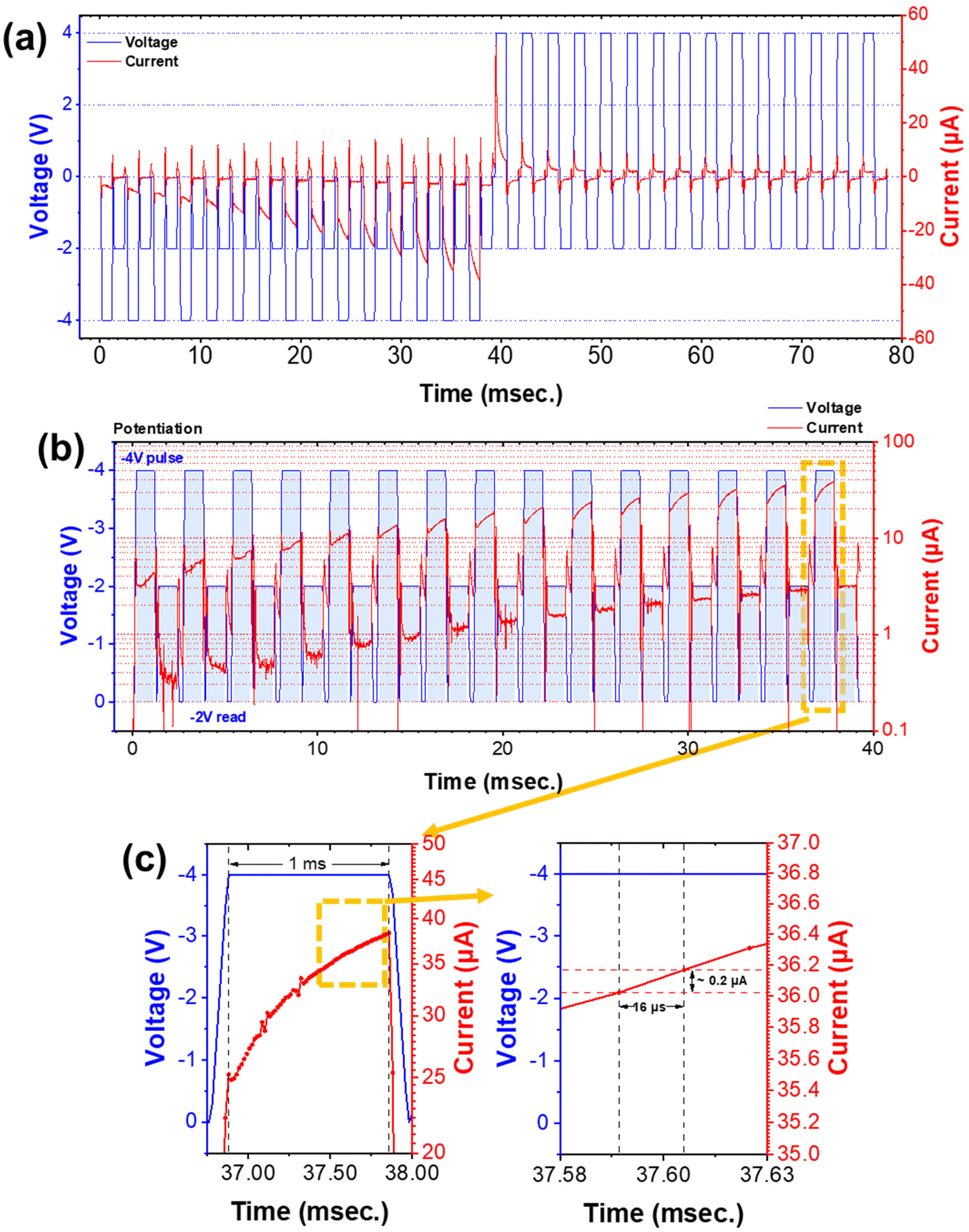 | ||
| Fig. 7 Pulse application results of (a) linear scale and (b) log scale in potentiation, and (c) enlarged image of last pulse of (b). | ||
As mentioned above, the highly linear and symmetric weight update is crucial for energy efficient and accurate pattern recognition capability. The pattern recognition accuracy was assessed using CrossSim Ver.2.0. Fig. 8(a) shows pulse data used in this simulation and Fig. 8(b) and (c) show the probability distribution of potentiation and depression by generating lookup tables, respectively. The CrossSim simulation program employs a numeric matrix update model, which takes experimentally measured potentiation and depression results and generates the ΔG vs. G plot, where G is the conductance.58 Then, it simulates the accuracy using the ΔG vs. G plot. For each pulse, the simulator finds the average update (ΔG) in the G state and its probability distribution. In addition, a part of the potentiation and depression weight results was chosen in the simulation for accuracy calculation to minimize the noise effect.63 In this simulation, 80% of the conductance range was used and the simulation result is given in Fig. 8(d). The pattern recognition accuracy of the device reached about 90.2% at the first epoch of training. This value is comparable to the simulation results of 97.3% under the condition of completely linear potentiation and depression with a uniform dynamic range, while maintaining all other input parameters the same. Higher accuracy in the completely linear case indicates that the improved linearity in potentiation and depression would realize even higher pattern recognition accuracy.
 | ||
| Fig. 8 (a) Pulse application results used in simulation, probability distribution of G (conductance) for (b) potentiation and (c) depression, and (d) pattern recognition accuracy. | ||
4. Conclusions
The Pt/p-LiCoOx/p-NiO/Pt memristor is proposed as an artificial synapse, devised to achieve a highly linear and symmetric weight update by forming a lower Schottky energy barrier with p-type oxides and high work function metals. The proposed device exhibited a highly linear and symmetric synaptic weight update for potentiation and depression, as well as the dependence of weight update on the pulse amplitude and pulse application number, PPF, and STP and LTP characteristics. These improved synaptic properties are thought to come from the Li+ ion redistribution within the NiO layer according to the bias condition. As a result of Li+ ion movement, the interface barrier between NiO and Pt BE was modulated, and then the potentiation and depression characteristics appeared accordingly. The application of negative pulse at the Pt TE depleted Li+ ions at the NiO/Pt(BE) interface, which reduced the energy barrier and consequently increased the conductance for hole charge transport as potentiation. Applying a positive pulse made Li+ ions near the Pt BE, resulting in an increased barrier and consequent resistance as depression. The pulse application showed a linear and continuous current change within 1 ms of width, demonstrating potential high-speed operation in the μs time range or even faster for weight update. The simulation of pattern recognition using the MNIST data set shows a learning accuracy of 90.4% after 15 epochs. Thanks to the use of fast and movable Li+ ions and an appropriately low energy barrier structure, the device enables a highly linear and symmetric weight update operation with a low voltage and high speed as an artificial synapse for neuromorphic computing systems.Author contributions
B. J. performed the device fabrication, electrical characterization, and TOF-SIMS analysis, and wrote the manuscript. P. H. C contributed to simulation execution and editing of the manuscript. J. H. and T. N. performed TEM analysis and contributed to the interpretation. T. S. Y conceptualized and supervised the project, all experiments, and the manuscript.Conflicts of interest
There are no conflicts to declare.Acknowledgements
This research was supported by the National R&D Program through the National Research Foundation of Korea (NRF) funded by the Ministry of Science and ICT (Grant No. NRF-2021M3F3A2A01037844), the Nano-Material Technology Development Program through the National Research Foundation of Korea (NRF) funded by the Ministry of Science and ICT (2022M3H4A1A04068923), the Korea Institute for Advancement of Technology(KIAT) grant funded by the Korea Government (MOTIE) (P0023703, HRD Program for Industrial Innovation) and the research project fund (1.210092.01) of UNIST (Ulsan National Institute of Science and Technology).References
- J. Tang, F. Yuan, X. Shen, Z. Wang, M. Rao, Y. He, Y. Sun, X. Li, W. Zhang, Y. Li, B. Gao, H. Qian, G. Bi, S. Song, J. J. Yang and H. Wu, Adv. Mater., 2019, 31, 1902761 CrossRef CAS PubMed.
- S. Jiang, S. Nie, Y. He, R. Liu, C. Chen and Q. Wan, Mater. Today Nano, 2019, 8, 100059 CrossRef.
- Q. Lu, F. Sun, L. Liu, L. Li, Y. Wang, M. Hao, Z. Wang, S. Wyang and T. Zhang, Microsyst. Nanoeng., 2020, 6, 84 CrossRef CAS PubMed.
- D. Kuzum, S. Yu and H.-S. Philip Wong, Nanotechnology, 2013, 24, 382001 CrossRef PubMed.
- Q. Wan, M. T. Sharbati, J. R. Erickson, Y. Du and F. Xiong, Adv. Mater. Technol., 2019, 4, 1900037 CrossRef.
- G. Rachmuth, H. Z. Shouval, M. F. Bear and C.-S. Poon, Proc. Natl. Acad. Sci. U. S. A., 2011, 108, E1266–E1274 CrossRef CAS PubMed.
- S. Moon, K. Park, P. H. Chung, D. P. Sahu and T.-S. Yoon, J. Alloys Compd., 2023, 963, 171211 CrossRef CAS.
- G. W. Burr, R. M. Shelby, A. Sebastian, S. Kim, S. Kim, S. Sidler, K. Virwani, M. Ishii, P. Narayanan, A. Fumarola, L. L. Sanches, I. Boybat, M. Le Gallo, K. Moon, J. Woo, H. Hwang and Y. Leblebici, Adv. Phys.: X, 2016, 2, 89–124 Search PubMed.
- H. Li, S. Wang, X. Zhang, W. Wang, R. Yang, Z. Sun, W. Feng, P. Lin, Z. Wang, L. Sun and Y. Yao, Adv. Intell. Syst, 2021, 3, 210017 Search PubMed.
- S. Yu, B. Gao, Z. Fang, H. Yu, J. Kang and H.-S. P. Wong, 2012 International Electron Devices Meeting, 2012.
- Q. Luo, X. Xu, T. Gong, H. Lv, D. Dong, H. Ma, P. Yuan, J. Gao, J. Liu, Z. Yu, J. Li, S. Long, Q. Liu and M. Liu, 2017 IEEE International Electron Devices Meeting (IEDM), 2017.
- W. Banerjee, X. Zhang, Q. Luo, H. Lv, Q. Liu, S. Long and M. Liu, Adv. Electron. Mater., 2018, 4, 1700561 CrossRef.
- S. Roy, G. Niu, Q. Wang, Y. Wang, Y. Zhang, H. Wu, S. Zhai, P. Shi, S. Song, Z. Song, Z.-G. Ye, C. Wenger, T. Schroeder, Y.-H. Xie, X. Meng, W. Luo and W. Ren, ACS Appl. Mater. Interfaces, 2020, 12, 10648–10656 CrossRef CAS PubMed.
- Z. Yong, K.-M. Persson, M. S. Ram, G. D’Acunto, Y. Liu, S. Benter, J. Pan, Z. Li, M. Borg, A. Mikkelsen, L.-E. Wernersson and R. Timm, Appl. Surf. Sci., 2021, 551, 149386 CrossRef CAS.
- V. Milo, C. Zambelli, P. Olivo, E. Pérez, M. K. Mahadevaiah, O. G. Ossorio, C. Wenger and D. Ielmini, APL Mater., 2019, 7, 081120 CrossRef.
- M. Azzaz, E. Vianello, B. Sklenard, P. Blaise, A. Roule, C. Sabbione, S. Bernasconi, C. Charpin, C. Cagli, E. Jalaguier, S. Jeannot, S. Denorme, P. Candelier, M. Yu, L. Nistor, C. Fenouillet-Beranger and L. Perniola, 2016 IEEE 8th International Memory Workshop (IMW), 2016.
- S. R. Lee, Y.-B. Kim, M. Chang, K. M. Kim, C. B. Lee, J. H. Hur, G.-S. Park, D. Lee, M.-J. Lee, C. J. Kim, U.-I. Chung, I.-K. Yoo and K. Kim, 2012 Symposium on VLSI Technology (VLSIT), 2012.
- M. Yu, Y. Cai, Z. Wang, Y. Fang, Y. Liu, Z. Yu, Y. Pan, Z. Zhang, J. Tan, X. Yang, M. Li and R. Huang, Sci. Rep., 2016, 6, 21020 CrossRef CAS PubMed.
- W. C. Chien, Y. C. Chen, K. P. Chang, E. K. Lai, Y. D. Yao, P. Lin, J. Gong, S. C. Tsai, S. H. Hsieh, C. F. Chen, K. Y. Hsieh, R. Liu and C.-Y. Lu, 2009 IEEE International Memory Workshop, 2009.
- J. Kim, J. Park and S. Kim, Materials, 2022, 15, 7185 CrossRef CAS PubMed.
- Y. Bai, H. Wu, Y. Zhang, M. Wu, J. Zhang, N. Deng, H. Qian and Z. Yu, Appl. Phys. Lett., 2013, 102, 173503 CrossRef.
- H. Y. Jeong, Y. I. Kim, J. Y. Lee and S.-Y. Choi, Nanotechnology, 2010, 21, 115203 CrossRef PubMed.
- J. Park, C. Lee, M. Kwak, S. A. Chekol, S. Lim, M. Kim, J. Woo, H. Hwang and D. Lee, Nanotechnology, 2019, 30, 305202 CrossRef CAS PubMed.
- D. Acharyya, A. Hazra and P. Bhattacharyya, Microelectron. Reliab., 2014, 54, 541–560 CrossRef CAS.
- S. Rehman, H. Kim, H. Patil, K. D. Kadam, R. U. Sagar, J. Aziz, D. Um, M. F. Khan and D. Kim, Adv. Electron. Mater., 2021, 7, 2001237 CrossRef CAS.
- A. M. Rana, T. Akbar, M. Ismail, E. Ahmad, F. Hussain, I. Talib, M. Imran, K. Mehmood, K. Iqbal and M. Y. Nadeem, Sci. Rep., 2017, 7, 39539 CrossRef CAS PubMed.
- J. Park and S. Kim, Results Phys., 2022, 39, 105731 CrossRef.
- C. Hu, Q. Wang, S. Bai, M. Xu, D. He, D. Lyu and J. Qi, Appl. Phys. Lett., 2017, 110, 073501 CrossRef.
- C. J. Park, S. W. Han and M. W. Shin, ACS Appl. Mater. Interfaces, 2020, 12, 32131–32142 CrossRef CAS PubMed.
- U. Russo, D. Ielmini, C. Cagli and A. L. Lacaita, IEEE Trans. Electron Devices, 2009, 56, 186–192 CAS.
- Y. Ahn and J. Y. Son, Ceram. Int., 2021, 47, 9342–9346 CrossRef CAS.
- Y. Ahn and J. Y. Son, Curr. Appl. Phys., 2023, 54, 44–48 CrossRef.
- J. Rao, Z. Fan, L. Hong, S. Cheng, Q. Huang, J. Zhao, X. Xiang, E.-J. Guo, H. Guo, Z. Hou, Y. Chen, X. Lu, G. Zhou, X. Gao and J.-M. Liu, Mater. Today Phys., 2021, 18, 100392 CrossRef CAS.
- K. Baek, S. Park, J. Park, Y.-M. Kim, H. Hwang and S. H. Oh, Nanoscale, 2017, 9, 582–593 RSC.
- S. Lashkare, V. Saraswat and U. Ganguly, ACS Appl. Electron. Mater., 2020, 2, 2026–2031 CrossRef CAS.
- S. Kim, S. Choi and W. Lu, ACS Nano, 2014, 8, 2369–2376 CrossRef CAS PubMed.
- W.-J. Chen, C.-H. Cheng, P.-E. Lin, Y.-T. Tseng, T.-C. Chang and J.-S. Chen, ACS Appl. Electron. Mater., 2019, 1, 2422–2430 CrossRef CAS.
- H. Ryu and S. Kim, Metals, 2021, 11, 440 CrossRef CAS.
- J. Woo, K. Moon, J. Song, S. Lee, M. Kwak, J. Park and H. Hwang, IEEE Electron Device Lett., 2016, 37, 994–997 CAS.
- Q. Wang, Y. Wang, R. Luo, J. Wang, L. Ji, Z. Jiang, C. Wenger, Z. Song, S. Song, W. Ren, J. Bi and G. Niu, Neuromorphic Comput. Eng, 2022, 2, 044012 CrossRef.
- C.-W. Hsu, Y.-F. Wang, C.-C. Wan, I.-T. Wang, C.-T. Chou, W.-L. Lai, Y.-J. Lee and T.-H. Hou, Nanotechnology, 2014, 25, 165202 CrossRef PubMed.
- G. Niu, M. A. Schubert, S. U. Sharath, P. Zaumseil, S. Vogel, C. Wenger, E. Hildebrandt, S. Bhupathi, E. Perez, L. Alff, M. Lehmann, T. Schroeder and T. Niermann, Nanotechnology, 2017, 28, 215702 CrossRef CAS PubMed.
- J. Yin, F. Zeng, Q. Wan, F. Li, Y. Sun, Y. Hu, J. Liu, G. Li and F. Pan, Adv. Funct. Mater., 2018, 28, 1706927 CrossRef.
- H. Tukamoto and A. R. West, J. Electrochem. Soc., 1997, 144, 3164–3168 CrossRef CAS.
- M. Thomas, P. Bruce and J. Goodenough, Solid State Ionics, 1985, 17, 13–19 CrossRef CAS.
- K. Nakamura, H. Ohno, K. Okamura, Y. Michihiro, I. Nakabayashi and T. Kanashiro, Solid State Ionics, 2000, 135, 143–147 CrossRef CAS.
- M. Kumar, Mater. Res. Express, 2019, 6, 096404 CrossRef CAS.
- T. Dutta, P. Gupta, A. Gupta and J. Narayan, J. Appl. Phys., 2010, 108, 083715 CrossRef.
- T. P. Mokoena, H. C. Swart, K. T. Hillie, Z. P. Tshabalala, M. Jozela, J. Tshilongo and D. E. Motaung, Appl. Surf. Sci., 2022, 571, 151121 CrossRef CAS.
- H. Wang, H. Yuan, J. Yu, C. Zhang, K. Li, M. You, W. Li, J. Shao, J. Wei, X. Zhang, R. Chen, X. Yang and W. Zhao, ACS Appl. Mater. Interfaces, 2020, 12, 53528–53536 CrossRef CAS PubMed.
- J. Wang, R. Zhu, Y. Gao, Y. Jia and G. Cai, J. Phys. Chem. Lett., 2023, 14, 2284–2291 CrossRef CAS PubMed.
- Y. Ting, J. Chen, C. Huang, T. Huang, C. Hsieh and W. Wu, Small, 2017, 14, 1703153 CrossRef PubMed.
- H. Sato, T. Minami, S. Takata and T. Yamada, Thin Solid Films, 1993, 236, 27–31 CrossRef CAS.
- J. Zhang, Y. Ji, Q. Gao, J. Gao, X. Geng, H. Li, H. Shi, M. Wang, Z. Xiao, P. K. Chu and A. Huang, Adv. Electron. Mater., 2022, 8, 2200269 CrossRef CAS.
- S.-M. Kim, S. Kim, L. Ling, S. E. Liu, S. Jin, Y. M. Jung, M. Kim, H.-H. Park, V. K. Sangwan, M. C. Hersam and H.-S. Lee, ACS Appl. Mater. Interfaces, 2022, 14, 5673–5681 CrossRef CAS PubMed.
- J. Meng, Z. Li, Y. Fang, Q. Li, Z. He, T. Wang, H. Zhu, L. Ji, Q. Sun, D. W. Zhang and L. Chen, IEEE Electron Device Lett., 2022, 43, 2069–2072 CAS.
- J. Cui, F. An, J. Qian, Y. Wu, L. L. Sloan, S. Pidaparthy, J.-M. Zuo and Q. Cao, Nat. Electron., 2023, 6, 292–300 CrossRef.
- T. P. Xiao, C. H. Bennett, B. Feinberg, M. J. Marinella and S. Agarwal, CrossSim: accuracy simulation of analog in-memory computing, GitHub, 2022, https://github.com/sandialabs/cross-sim Search PubMed.
- Y. LeCun, C. Cortes and C. J. C. Burges, The MNIST database of handwritten digits, 1998, https://yann.lecun.com/exdb/mnist.
- J. Woo and S. Yu, IEEE Nanotechnol. Mag., 2018, 12, 36–44 Search PubMed.
- W.-L. Jang, Y.-M. Lu, W.-S. Hwang and W.-C. Chen, J. Eur. Ceram. Soc., 2010, 30, 503–508 CrossRef CAS.
- K. Park, P. H. Chung, D. P. Sahu and T.-S. Yoon, Mater. Sci. Semicond. Process., 2022, 147, 106718 CrossRef CAS.
- J. Fuller, F. E. Gabaly, F. Léonard, S. Agarwal, S. J. Plimpton, R. B. Jacobs-Gedrim, C. D. James, M. J. Marinella and A. A. Talin, Adv. Mater., 2016, 29, 1604310 CrossRef PubMed.
| This journal is © The Royal Society of Chemistry 2024 |