
 Open Access Article
 This Open Access Article is licensed under a
 Creative Commons Attribution 3.0 Unported Licence
A computational model for a molecular chemical sensor†
Mengxuan
Li
 a,
Clotilde S.
Cucinotta
b and
Andrew P.
Horsfield
*a
a,
Clotilde S.
Cucinotta
b and
Andrew P.
Horsfield
*a
aDepartment of Materials, Imperial College London, South Kensington Campus, London SW7 2AZ, UK. E-mail: a.horsfield@imperial.ac.uk
bDepartment of Chemistry, Imperial College London, White City Campus, 82 Wood Lane, London W12 0BZ, UK
First published on 14th February 2024
Abstract
In this study, we propose that a molecular junction with a sharp Negative Differential Resistance (NDR) current peak could improve the selectivity, thereby functioning as a potential molecular sensor for molecule recognition. Using DFT–NEGF simulations, we investigate the connection between molecule–molecule coupling, molecule–electrode coupling and the corresponding NDR peak shape. Based on this analysis we propose three design rules to control the sensitivity of a sensor and determine that one mechanism for NDR is for a localised molecular orbital involved in resonant tunneling to enter and leave the bias window. Our findings provide useful insight into the development of single molecule sensors for molecule recognition.
1 Introduction
There are two leading theories behind the smell mechanism in humans: vibrational theory and shape theory. The shape theory, also known as lock and key theory, states that a receptor in the olfactory system will only be activated if the shape of a molecule matches that of the receptor, like a key fitting into a lock.1 In contrast, the vibrational theory, first proposed by Dyson in 1928 and later provided with a mechanism by Turin in 1996, argues that it is the vibrational frequency of the molecule which characterise them, and which activate the olfactory receptors.2 According to this theory, molecules with the same vibrational frequencies will smell alike, while the shape theory suggests that molecules with similar shapes will have a similar odour.The central idea of the Turin mechanism for the vibrational theory is the generation of an inelastic electron tunneling spectrum and, therefore, is considered to be eligible to realize a physical chemical sensor for molecule recognition. To explore the possibility of chemical sensors based on the vibrational theory of olfaction, Patil modelled a molecular wire using a tight-binding Hamiltonian with nearest neighbor hopping.3 This wire was connected to two semi-infinite leads, forming a molecular junction. The Inelastic Electron Tunnelling Spectroscopy (IETS) spectrum exhibited a clear peak at 0.15 V, which appears due to the addition of an external molecule, in addition to the largest peak which belongs to the molecular wire. This additional peak demonstrated the functionality of this chemical sensor to detect external molecules. Later in 2018, Patil replaced the molecule wire with a molecular Resonant Tunneling Diode (RTD) using the same framework.4 In this way, he overcame the drawback that the operation of IETS requires cryogenic temperatures to avoid thermal broadening of spectrum peaks, proving that the molecular RTD could be a promising sensor at room temperature. While Patil's work shows great promise in this field, all the sensors he studied are theoretical models but not real molecules. Following Patil's study, Sahoo inserted a real molecule RTD put forward by Perrin5 into this sensor configuration and successfully recognised hydrogen cyanide and benzaldehyde through IETS.6
Although the mechanism of vibration detection is close to that of IETS, with both vibrational theory and IETS involving inelastic electron tunnelling, the recognition system of the sensor inspired by vibrational theory does not necessarily depend on the conventional IETS peaks found in the second derivative of the current–voltage (I(V)) response. Traditional IETS is conducted using metal–insulator–metal junctions. To resolve thermal broadening problems which affect the peak resolution it needs to be operated at a cryogenic temperature which is a strict operation condition. The current prevailing solution to resolve the resolution problem at higher temperature is to utilize machine-learning algorithms to discriminate between compounds on the raw data produced from the sensors.7–10
However, if the junction is reduced to the molecular level, the orbitals will be well separated in energy due to quantum confinement. This makes it possible for the movement of electrons through the highly quantised orbitals to be affected by the applied voltages to generate peaks directly in the I(V) curve instead of in d2I/dV2, as normally used in IETS. To generate the peaks, the molecule must exhibit negative differential resistance.
Negative differential resistance (NDR) is a phenomenon where the current decreases as the applied bias to the device increases, whereas in conventional devices the current increases linearly with the increase in applied bias. This phenomenon can occur when two narrow energy states, each pinned to separate electrodes, are present in the junction. In this case, let's consider the two states to be the highest occupied molecular orbital (HOMO) of a molecular donor present in the junction and the lowest unoccupied molecular orbital (LUMO) of a molecular acceptor, as depicted in Fig. 1. At low bias, an energy gap between the HOMO and LUMO prevents electron tunneling between them (Fig. 1a), resulting in a low current. As a positive bias is applied, the HOMO rises and the LUMO drops following the potential shifts in the electrodes they are pinned to, until a bias is reached when the HOMO and LUMO move into resonance (Fig. 1b), resulting in a maximal current. However, if the bias continues to increase, the HOMO and LUMO will move out of resonance again causing the pathway generated by their resonance to disappear (Fig. 1c). The current thus drops and a peak is generated in the I(V) curve, as shown in the primary peak in Fig. 1(d). If the gap between the HOMO and LUMO corresponds to the vibrational energy of an external molecule, an additional peak would appear at the voltage which differs from the primary peak by exactly the vibrational energy, as the smaller peak in Fig. 1(d) shows.
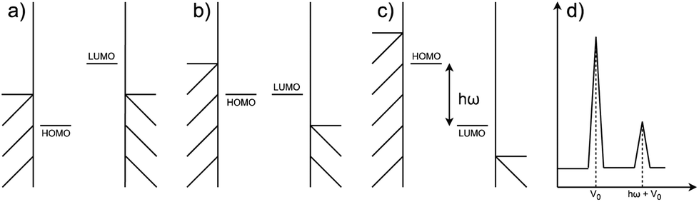 | ||
| Fig. 1 An illustration of the NDR mechanism. (a) Molecular junction at 0 V; (b) the resonance state; (c) the HOMO–LUMO gap corresponds to a vibrational energy of the external molecule; (d) the I(V) curve. | ||
Despite significant research on molecular electronics based on IETS,11–17 less work has been done to investigate the use of IETS in molecular electronics as a mechanism of chemical sensing, and in particular to focus on the I(V) characteristic of the sensor device, rather than the second derivative of the I(V). One particular problem for the I(V) characteristics of such sensor devices is that their sensitivity is determined by the NDR shape. If the NDR peak is too broad, the additional peak introduced by external molecules will be invisible, making the process of recognition difficult and decreasing the sensitivity of the chemical sensor.
To explore ways to manage this broadening, in this work we design a simple molecular sensor model, and study the relationship between the features of the molecular sensor and the shape of NDR peaks in the I(V) curve. We develop three simple conditions to control device sensitivity and how our simple models meet these three conditions. Our research demonstrates the viability of a single molecule chemical sensor in which the recognition system is based only on the I(V) curve, and sheds light on molecular transport mechanisms and molecular electronics engineering. However, limitations of our models and calculations do exist and are discussed in later sections.
2 Results
We have created a simple model for the molecular resonant tunneling diode sensor, consisting of the molecular junction shown in Fig. 2. For the purpose of developing optimal design rules, we have partitioned the molecular junction into five functional sites: a bottom anchoring group, a donor site (bottom site), a bridging group, an acceptor site (top site), and a top anchoring group. We initially utilized two benzene molecules as the donor and acceptor and a saturated carbon chain as the decoupling units. By adjusting the lengths of bridge and anchoring groups we quantitatively analysed the effect on the I(V) curve intensity and peak shape of the coupling strength between the molecular moieties and between the molecules and electrodes. We note that the proposed model represented in Fig. 2 just depicts the sensor molecule and does not include the odorant. | ||
| Fig. 2 The simplified model composed of a bottom anchoring group, a donor site (bottom site), a bridging group, an acceptor site (top site), and a top anchoring group. The left and right boundaries represent for the bottom and top electrodes. | ||
Based on this analysis we propose three design rules to control the sensitivity of the molecular resonant tunneling diode we have designed as a chemical sensor: (1) weak coupling between molecular donor and molecular acceptor. (2) Weak coupling between the molecules and the electrodes. (3) Proximity of HOMO of the acceptor to the Fermi energy of the electrodes.
Before we discuss the design rules, let's first understand the “pinning” mechanism, which involves electron interaction between two orbitals. When two partially filled orbitals come in contact reach equilibrium, any increase in the energy of one orbital leads to an electron flow from it to the other orbital. This flow will cause the first orbital to lower its energy due to reduced electron repulsion, and the second orbital to raise its energy due to increased electron repulsion. As a result, the two levels realigns, though with different charges. When there is insufficient electron flow between the orbitals to keep them aligned, then the two orbitals move out of alignment, and the pinning is broken. This electronic interaction exists not only between orbitals localised on electrodes and molecules but also between different molecular moieties.
2.1 First condition: weak coupling between molecular donor and molecular acceptor
As mentioned before, the generation of NDR involves the interaction of HOMO and LUMO orbitals, localized on the donor site (bottom aromatic group) and the acceptor site (top aromatic group) within our molecular junction, and each pinned to different electrodes. At the potential when they reach resonance, these frontier orbitals become connected and spread over the whole molecular junction. This wide range of overlap results in broad peaks and therefore reduced sensor sensitivity. Our first rule to guarantee sensitivity and selectivity of the sensor, is to minimise the coupling between the donor the acceptor site within the junction.To decouple the donor and acceptor we introduced a saturated carbon chain of increasing length in the bridging area. The length of this carbon chain affects the strength of this coupling. A weak coupling decreases conjugation between the donor and the acceptor resulting in a reduced energy range for electron transmission, and narrowing the NDR peak.
We label these molecular junctions as ben–ben0X0, where X denotes the number of CH2 groups in the bridging region, ranging from 1 to 4 CH2 groups. Note that here (CH2)n refers to the group in a saturated chain, as opposed to the ethyne molecule. The resulting I(V) curves are shown in Fig. 3. By analysing the figure, two distinct types of I(V) characteristics can be observed: for chains with fewer than three CH2 groups, the corresponding I(V) curves exhibit NDR peaks near 2 V, which however are still broad. The emergence of a NDR peak around 2 V can be attributed to the pinning of the molecular orbitals of the sensor to the electrodes under applied bias. In particular, the HOMObottom would not fall within the bias window until 2 V is reached. At this bias, the current reaches its maximum value. Beyond this bias, the HOMOtop and HOMObottom levels move in opposite directions with increasing bias and leave the resonant state, leading to a decline in the current. When the chain length is above 3 CH2 groups the NDR peak reduces, and only small fluctuations are observed in the I(V) curve.
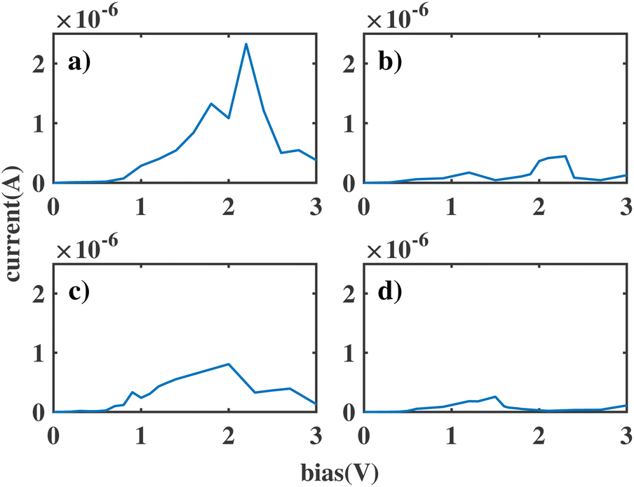 | ||
| Fig. 3 The current through the double benzene molecule as a function of applied bias voltage for the following models: (a) ben–ben010; (b) ben–ben020; (c) ben–ben030; (d) ben–ben040. | ||
This length-related feature can be explained in terms of the density of states projected over the two molecules (PDOS), as shown in Fig. 4 for each bridge length and a bias of 2 V. When the bridge length is three or fewer CH2 groups, the coupling between the HOMO of the top (HOMOtop) and bottom (HOMObottom) benzene molecules is still strong, causing them to stay pinned and the peak to remain broad. In particular HOMObottom remains in proximity of the lower boundary of the bias window at −1 eV. However, when the bridge length increases to four CH2 groups, the coupling between molecules reduces, and the HOMObottom becomes pinned to the potential of the bottom electrode. As a result, the HOMObottom is free to shift rapidly to a higher energy position as a positive bias is applied to the bottom electrode. Since the coupling between donor and acceptor is in this case small, we will take four CH2 groups as the optimal bridge length. Therefore, ben–ben040 is utilized as the template bridge length in the following calculations and discussions.
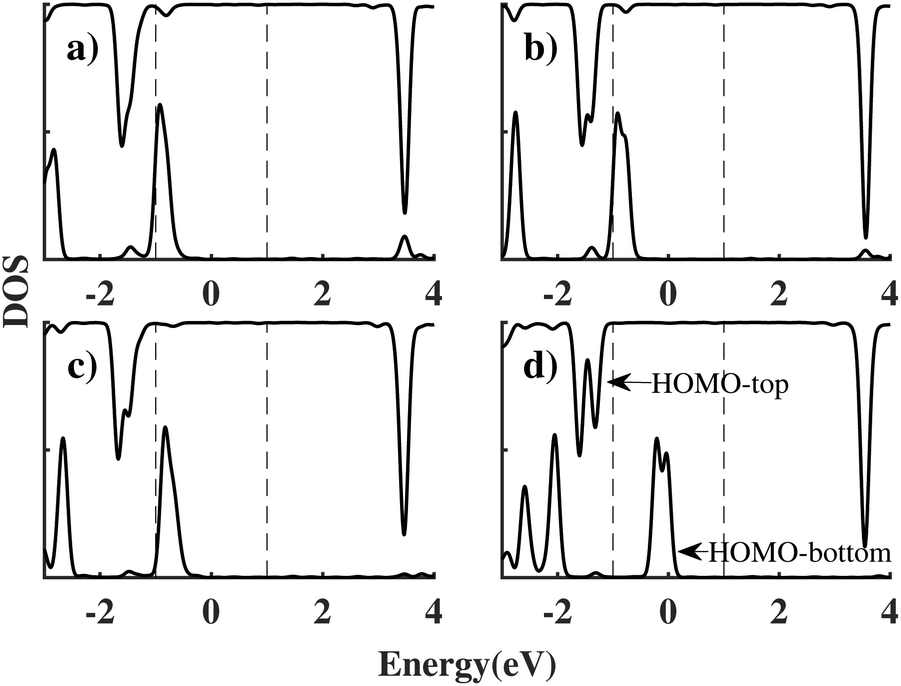 | ||
| Fig. 4 The PDOS of ben–ben models at 2 V (a) ben–ben010 (b) ben–ben020 (c) ben–ben030 (d) ben–ben040. The black dotted lines indicate the boundaries of the bias window, which spans from −1 to 1 eV at 2 V. The highest energy peaks in the upper and lower curve represent the HOMO of the top (HOMOtop) and bottom (HOMObottom) benzene molecules, respectively. | ||
Another important observation is that the current in our junction keeps dropping with increasing number of CH2 groups in the bridge. This is because, besides decoupling donor and acceptor, the saturated carbon groups act as insulators between the bottom and top contacts. As a result, the resistance of the entire molecule increases. For this reason it is important to find a balance in the length of the bridge: if the bridge is too long, the resistance of the molecular sensor becomes too high, and the current is no longer detectable. To be noted, the non-linear reduction of current as a function of the chain length, particularly ben–ben020 and ben–ben030, is due to the different geometries of the sensor molecule with odd and even number of CH2 groups in the bridge. The change in geometry affects the electron transport as explained and illustrated in the ESI S1 Fig. 4 and 5.†
2.2 Second condition: weak coupling between the molecules and the electrodes
An anchoring group is a linker used to connect the molecule and the electrodes in a molecular junction. The connection between the metal contacts and the sensor molecule also influences the broadening: strong coupling allows greater transmission of the metal states through the molecule, increasing the broadening. In the calculations above we inserted a 3 Å vacuum gap between the molecule and the gold electrodes: this roughly corresponds to contact with an STM tip. To study the effect of anchoring groups, thiols were added to both ends of the template molecule and attached to the junction, labelled ben–ben040s.The I(V) curve in the presence of the thiol groups is shown in Fig. 5(a). A peak, which is generated when the HOMObottom and LUMOtop are in resonance as shown in Fig. 6, appears at 5.2 V, which is approximately the HLG of benzene. This peak, however is quite broad due to the newly inserted thiols which bridge the gap between molecule and electrodes, increasing the molecule–electrode coupling and broadening the frontier orbitals because of the eased electron transport. In other words, the current increased even if the HOMObottom and LUMOtop move out of resonance, as the tails of these two broadened levels can still contribute to the coupling between the moieties, resulting in an increment of the current.
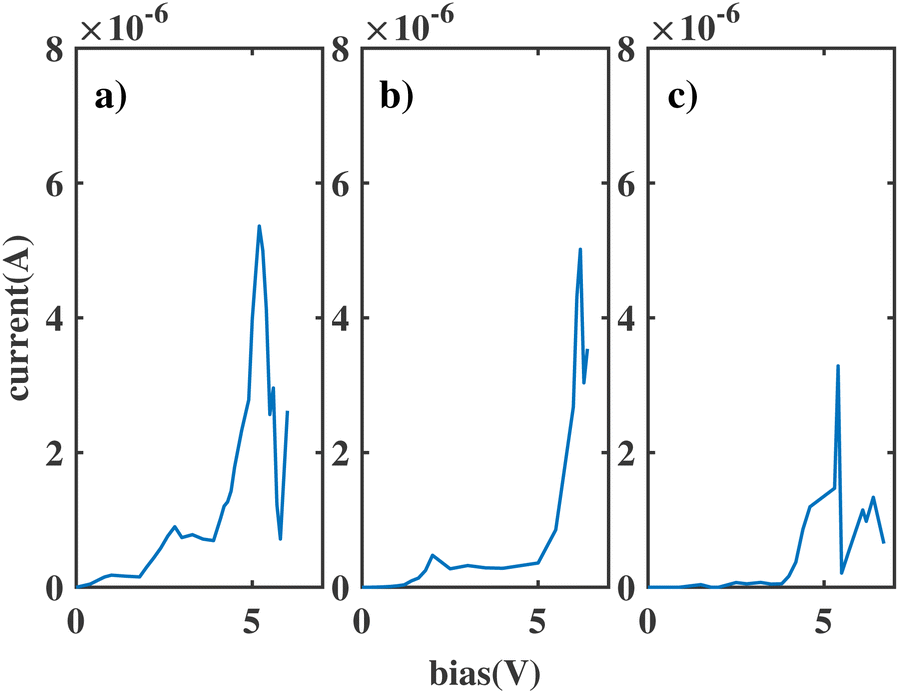 | ||
| Fig. 5 The current of ben–bens models (a) ben–ben040s (b) ben–ben141s (c) ben–ben242s. | ||
 | ||
| Fig. 6 The PDOS of ben–ben040s model at 0 V and 5 V. HOMObottom and LUMOtop which generate the NDR peak are labelled. The arrows show how the orbitals move when a positive bias is applied. | ||
The strength of the coupling between the molecule and the electrode can be modulated by modifying the anchoring group. One way to reduce the coupling strength and obtain a narrower peak is to insert CH2 groups in anchoring groups since saturated C atoms are effective decoupling units. One CH2 group and two CH2 groups were inserted in both ends of the previous thiol model, forming the S–CH2 and S–CH2–CH2 linkers. The I(V) curves for these two new models, labelled ben–benX4Xs, where X represents the number of CH2 groups in the anchoring groups (X = 1 or 2), are shown in Fig. 5; their corresponding peaks are both sharper than that of the previous thiol model.
These NDR peaks are sharp, however their positions are shifted to an even higher bias compared with that of ben–ben040s. The shift towards higher bias is a consequence of the reduced molecule–electrode coupling produced by the insertion of the CH2 groups, which results in reduced bias control of the electrode over the relevant molecular orbitals, and therefore a higher bias for these orbitals to reach resonance, as explained below.
To explain this concept and quantify the pinning of molecular orbitals to the electrode over the molecular system, we introduce the efficiency factor, E. This factor represents the ratio between the shift of frontier orbitals compared with their positions at 0 V and the shift of the electrode potential, as shown in the following equation.
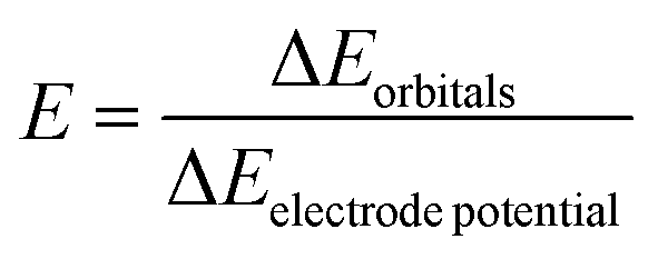 | (1) |
| Model | E |
|---|---|
| ben–ben040s | 93.1% |
| ben–ben141s | 70.2% |
| ben–ben242s | 63.3% |
| ben–ben040 | 59.3% |
2.3 Third condition: proximity of the HOMO of the acceptor to the Fermi energy of the electrodes
Despite a sharp NDR peak being observed in the Fig. 5(b) and (c) of our simplified model sensor, the voltage where this sharp NDR peak is located is too large to be realized in an experimental molecular junction. Indeed, a voltage of 5.2 V or more, which corresponds to the location of the sharp NDR peak in our model, can potentially compromise the stability of the molecular contacts, or even cause the molecular junction to break down.18 Therefore, we need to take measures to alter the position of the NDR peak.One way to alter the position of the NDR peak is to replace the top benzene with a different acene molecule, such as naphthalene, anthracene or tetracene. These all have a smaller HOMO–LUMO gap than benzene, thus the location of the frontier orbitals is closer to the Fermi level than that of benzene, leading to a difference between HOMOs of the bottom and top moieties. On the basis of this difference, it is the HOMObottom and HOMOtop, not the HOMObottom and the LUMOtop, that come to resonance within the bias window. The voltage required for resonance is reduced significantly as the energy difference between the two HOMO levels is much smaller than the HLG of the benzene, as shown in Fig. 7.
 | ||
| Fig. 7 (a) HOMObottom–HOMOtop coupling. The HOMObottom and HOMOtop belong to the benzene moiety and the anthracene moiety respectively. (b) HOMObottom–LUMOtop coupling. The HOMObottom and LUMOtop belong to the bottom benzene moiety and the top benzene moiety respectively. | ||
We substituted an anthracene to the top benzene group of ben–ben040 and calculated the I(V) curve of the resulting molecule, as shown in Fig. 8. A sharp NDR peak is observed near 1.65 V. After checking the corresponding PDOS in Fig. 9 of this new molecule, which is labelled ben–ant, we find that this sharp NDR peak is exactly a consequence of the interaction between the HOMO of the benzene, depicted in black, and the HOMO of the anthracene, depicted in red, instead of the LUMOtop, as seen in the ben–ben case.
 | ||
| Fig. 8 The variation with voltage of the current through the sensor molecule with the top benzene replaced by anthracene. | ||
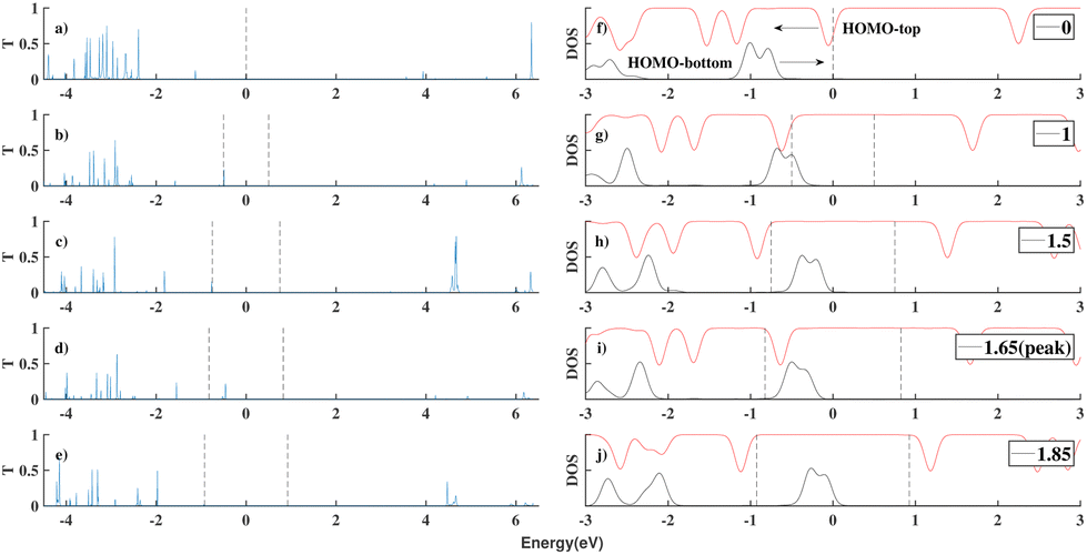 | ||
| Fig. 9 The transmission plot and the PDOS of ben–ant models under different voltages (a and f) 0 V (b and g) 1 V (c and h) 1.5 V (d and i) 1.65 V (the position of the NDR peak) (e and j) 1.8 V. The PDOS of the anthracene moiety is in red and the PDOS of the benzene is in black. The orbitals that are concerned has been labelled as HOMObottom and HOMOtop which belong to the benzene moiety and the anthracene moiety respectively. The arrows show how the orbitals move when a positive bias is applied. | ||
The generation of this sharp NDR peak involves the entrance and exit of the HOMOtop in the bias window. The PDOS shift under bias clearly shows the two movements of the HOMOtop, as shown in Fig. 9. At 0 V, the HOMOtop is quite close to the Fermi level of the electrodes. After a drop in the potential of the top electrode due to the applied positive bias, the energy of the HOMOtop also goes down, leading to a declining HOMObottom–HOMOtop gap. At a bias of 1 V, the HOMO–HOMO gap reached 0 but we would only expect a small current boost here because the majority of both HOMOs are out of the bias window, as shown in Fig. 9(g). However, after all of the HOMObottom enters the bias window, the HOMOtop suddenly is able to carry current, and hence accumulate charge, and returns to its previous position which has a higher energy within the bias window. In this case, the resonance of the HOMObottom and HOMOtop takes place within the bias window and a channel for electrons is generated, boosting the current at 1.65 V, as shown in Fig. 9(i).
The unique resonance occurring at 1.65 V can also be observed in the charge distribution of the model, as shown in Fig. 10. With an increasing applied bias, the charges on the benzene (anthracene) increase (decrease) as the fragment is close to the bottom (top) electrode until 1.65 V is reached. At this bias, the resonance of HOMObottom with HOMOtop takes place and charges on these two fragments redistribute. The negative charges on the benzene flow to the anthracene, accompanying the electron transport and boosting the current. What this redistribution process exhibits in the charges versus bias figure is a peak or a valley at 1.65 V.
 | ||
| Fig. 10 The charge distribution of the ben–ant model. Black: the Hirshfeld charge on the benzene fragment. Red: the Hirshfeld charge on the anthracene fragment. | ||
The sudden entrance and exit of the HOMOtop from the bias window requires two conditions. The coupling between the electrode and the molecule should not be too strong, and the HOMOtop should be close to the Fermi energy of the top electrodes, which is our third condition. For the second condition, until the coupling is strong, the energy of HOMOtop would be mainly controlled by the electrode and the HOMO is pinned to the electrode. As a consequence the energy level would keep decreasing, following the electrode Fermi energy. This situation is observed when the ben–ant groups are strongly linked to the electrode through a thiol, as shown in the ESI S1 Fig. 1.†
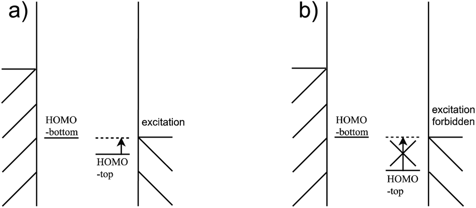
For the third condition, the HOMOtop should be close to the Fermi energy of the electrodes so that the difference between HOMOtop and electrode Fermi energy is small when the HOMObottom enters the bias window, as Fig. 11(a) shows. And the coupling between the HOMObottom and HOMOtop could trigger the excitation of the HOMOtop by current carrying electrons, as shown in Fig. 9(i). By contrast, the HOMObottom enters the bias window when there is a large energy gap between the levels of these two moieties, and the HOMObottom would not overcome the energy gap and never be able to carry a current, as shown in Fig. 11(b). It should be noted that the strong coupling between the molecule and the electrode would compress the HOMO–LUMO gap of the molecule to a much smaller value compared to that of the isolated molecule due to the pinning effect.19 However, this way to reduce the energy difference between the HOMO of the molecule and electrode chemical potential is not viable as the interaction between molecule and electrode is strong, violating the second condition.
 | ||
| Fig. 11 The HHG is (a) small (b) big when the HOMObottom enters the bias window. | ||
In the previous paragraph, we mentioned that the excitation of the HOMOtop is triggered by the coupling between the moieties, which seems to contradict the requirement that the coupling between the moieties should be weak. However, it is exactly the weak molecule–molecule coupling that enables the sudden shift of the HOMOtop. Otherwise, the orbital would just stick to the position and not move freely if the molecule–molecule coupling is strong.
A NDR peak at a smaller voltage not only originates from a smaller gap but also the suppression of electrode Fermi energy to the molecular orbitals. The movement of the HOMOtop goes through two stage. At the first stage in the Fig. 12(a), the movement of HOMOtop is insignificant compared with the movement of the electrode Fermi energy by the bias as the coupling between the molecule and electrode is weak. The gap between the HOMOtop and corresponding electrode Fermi energy then is expected to diminish. Soon the energy level of the HOMOtop would be the same as the Fermi energy of the electrode and this orbital would enter the second stage in the Fig. 12(b).
 | ||
| Fig. 12 The movement of the HOMOtop (a) slow shift (b) fast shift, catching up with the shift of the electrode and reaching an efficiency of 100%. | ||
At the second stage, the movement of the HOMOtop is fast. As the electrode Fermi energy drops, electrons from the nearby HOMO escape from the moiety to the electrode as it is the only electron-rich channel above the electrode potential. The drain of the electrons would decrease the level energy because of the self-interaction of the electrons within the orbital, and, in this way, the contribution of this level to electron transport would be suppressed by the change in the electrode Fermi energy. That is, the movement of the level would catch up with the movement of the electrode potential, boosting the rate of change of orbital energy.
If we now replaced the acceptor site with a LUMO-alignment moiety, that is the LUMO of the moiety is quite close to the Fermi level of the electrodes and its HOMO is lower than that of benzene, the NDR peak is generated through HOMObottom–LUMOtop coupling. Even if the energy of the LUMOtop is much lower than the LUMO of the benzene above, the movement of the LUMOtop is still quite slow without a strong coupling between the molecule and the electrode and suppression of the electrode potential. As the LUMOtop is always above its corresponding electrode Fermi energy and no electrons locate on the LUMOtop, the drop of the electrode potential would not affect the behavior of the LUMOtop which would just shift at quite low efficiency.
We have also tried another way to modify the HOMObottom and LUMOtop gap by adding electron extraction groups, –F, to the top benzene molecule in the model. The role of the electron extraction groups here would be analogous to that of a n-type dopant in a semiconductor, which moves conduction bands towards the Fermi level. The projected density of state on the top and bottom benzenes of these modified molecules are shown in ESI S1 Fig. 2 and 3.† However, we find that the effect of the added functional groups is not large. The magnitude of the reduce of the HOMObottom and LUMOtop gap is relatively small, compared with that of the large HOMO–LUMO gap (HLG) of the benzene, 5.2 eV.
Just as we did for the ben–ben models, an anchoring group was added to either side of the ben–ant model respectively to build a molecule–electrode connection, which makes it more like a practical sensor rather than an STM experiment. In order to meet the second conditions, only –SCH2CH2 was applied as the extra two CH2 groups have been proven to weaken the molecule–electrode coupling which has already been seen in the ben–ben models where the efficiency E of ben–ben242s is the comparable to that of ben–ben040, as shown in Table 1.
The I(V) curve of the ben–ant model with weak anchoring groups is shown in Fig. 13. As expected, a sharp NDR peak is observed at 2.5 V, as also seen in the models with vacuum. The aforementioned HOMObottom–HOMOtop crossover which occurs outside of the bias window is also observed in the PDOS figure and transmission curve, followed by the entrance of the HOMOtop to reach the resonance between the two moieties. Reproducing the specific type of a sharp NDR peak with solid anchoring groups supports our hypothesis and makes our three conditions more practical and realizable for a physical chemical sensor.
 | ||
| Fig. 13 The current of ben–ant242. | ||
We note that there are some limitations to our models and calculations. Although our calculations and results support the viability of a single molecule molecular sensor which relies on the sharp NDR peaks of I(V) curves to recognise external molecules, we don't know how this peak would be affected once more interactions are involved. The electron–phonon interactions are out of the scope of this paper and we are just focusing on the elastic condition for sensing. As the electron–phonon interaction between molecules and receptors is basically the central idea of the vibrational theory of smell mechanisms, it needs to be explored for the completeness of the performance of our sensors, and will be addressed in our future work. Our model is primarily based on a vacuum environment to isolate the fundamental electronic properties of the sensor material without external interference. In reality O2 and other air components may affect the sensor performance e.g. affecting the concentration of the odorant, interacting with the sensor inelastically and contributing to background noise in the I(V) characteristic. The effect of environmental factors will also be discussed in future work.
3 Conclusions
In this work, we have derived a simple model which is composed of five functional sites: a bottom anchoring group, a bottom moiety, a bridge, a top moiety, and a top anchoring group. By tweaking the number of CH2 groups in the bridge sites and between the molecule and the contacts, we have investigated the effect of the molecule–electrode coupling and molecule–molecule coupling on the current of this molecular junction. A sharp NDR peak resulting from the shift of the HOMO was observed when the two coupling interactions are both weak.Three design rules are suggested to be realized in a successful sensor: (1) weak coupling between molecular donor and molecular acceptor. (2) Weak coupling between the molecules and the electrodes. (3) Proximity of HOMO of the acceptor to the Fermi energy of the electrodes. Our findings provide insights for molecular engineering and could support a new single molecular sensor which recognizes molecules merely relying on its I(V) characteristics instead of the traditional IETS spectrum that is based on the second derivative of the current with respect to the bias.
One note of caution when applying our three rules is that strength of the current across the junction and the sharpness of the NDR peaks are influenced in opposite ways by the strength of the couplings: reducing the coupling of the molecule to the contact reduces the current as well as sharpening the resonances. If the couplings are too weak the current could be too small to detect and the meaningful peak would be immersed in the background noise. Finding the right balance in the coupling strength is crucial to ensure both detectable current and well-defined NDR peaks.
4 Methodology
Geometry optimization for all the structures was conducted through the CP2K DFT code,20 version 8.2, using Goedecker, Teter, and Hutter (GTH) norm-conserving pseudopotentials21 and triple zeta valence polarized basis sets, except for gold atoms for which we used a single zeta polarized basis set. As a 5 × 5 atom slab of gold makes up an electrode in our system, it is necessary to use a single zeta basis to reduce the computational resources consumed, while retaining sufficient accuracy. The cutoff energy for the density mesh is 500 Ry and a 9 × 9 × 1 mesh of k-points is used. All the convergence parameters were determined through a series of convergence test calculations, reaching an error of 0.001 eV per atom.The following procedure was used to determine the relaxed geometry. An isolated molecule is optimized first to determine the relaxed distance between the top and bottom atoms. Electrodes are then added above and below the outermost atoms with a vacuum of 3 Å between the electrode and the outermost atoms. The vacuum reduces the interaction between the molecule and the electrodes so that we could focus on the effect of the length of bridging group between the two aromatic molecules on the current through the molecular junction. It roughly corresponds to an experiment using an STM tip as a contact. If the vacuum is replaced with a thiol the distance between the gold electrode and the top sulfur or the bottom sulfur is fixed to 1.7 Å. In this case the distance between the top and the bottom electrodes is 2 × 1.7 Å plus the distance between the top and the bottom atoms of the molecule obtained in the isolated molecule optimization stage. Finally, the molecule–electrode junction is optimized until the forces fall below 10−4 a.u.
NEGF calculations for transport properties, such as current and transmission spectrum, were carried out as implemented in CP2K version 8.2.22 Further postprocessing analysis such as the projected density of states under finite bias calculations were carried out in the modified version of CP2K 8.2 created by Dr Sergey Chulkov. He has also demonstrated the reliability of the NEGF formalism in CP2K by calculating the I(V) curve of dithiol benzene with gold electrodes22 and comparing the results with those presented in earlier work:23 the results are found to be consistent.
Author contributions
Mengxuan Li: investigation, data curation, writing – original draft. Clotilde S. Cucinotta: methodology, writing – review & editing, supervision. Andrew P. Horsfield: conceptualization, methodology, writing – review & editing, supervision.Conflicts of interest
There are no conflicts to declare.Acknowledgements
Via our membership of the UK's HEC Materials Chemistry Consortium, which is funded by EPSRC (EP/L000202), this work used the UK Materials and Molecular Modelling Hub for computational resources, MMM Hub, which is partially funded by EPSRC (EP/T022213/1, EP/W032260/1 and EP/P020194/1). We are also grateful to Imperial College Research Computing Service for their computational resources. We acknowledge the Thomas Young Centre under grant number TYC-101. C. S. C. acknowledges funding from EPSRC grant EP/P033555/1. We thank Dr Sergey Chulkov for his modified version of CP2K version 8.2 to enable printing the projected density of states under finite bias calculations.Notes and references
- J. Amoore, Nature, 1967, 214, 1095–1098 CrossRef CAS PubMed.
- J. C. Brookes, F. Hartoutsiou, A. Horsfield and A. Stoneham, Phys. Rev. Lett., 2007, 98, 038101 CrossRef PubMed.
- A. Patil, D. Saha and S. Ganguly, 2016 IEEE 16th International Conference on Nanotechnology (IEEE-NANO), 2016, pp. 12–14.
- A. Patil, D. Saha and S. Ganguly, Sci. Rep., 2018, 8, 128 CrossRef PubMed.
- M. L. Perrin, E. Galan, R. Eelkema, F. Grozema, J. M. Thijssen and H. S. J. van der Zant, J. Phys. Chem. C, 2015, 119, 5697–5702 CrossRef CAS.
- S. Sahoo, N. Pandey, D. Saha and S. Ganguly, 2018 International Conference on Simulation of Semiconductor Processes and Devices (SISPAD), 2018, pp. 34–37.
- M. A. H. Khan, B. Thomson, R. Debnath, A. Motayed and M. V. Rao, IEEE Sens. J., 2020, 20, 6020–6028 CAS.
- L. Xu, J. Zhang, L. Cao and X. Hu, 2021 IEEE 6th International Conference on Signal and Image Processing (ICSIP), 2021, pp. 1215–1218.
- L. Bian, D. C. Sorescu, L. Chen, D. L. White, S. C. Burkert, Y. Khalifa, Z. Zhang, E. Sejdic and A. Star, ACS Appl. Mater. Interfaces, 2018, 11, 1219–1227 CrossRef PubMed.
- N. Pandey, D. Pal, D. Saha and S. Ganguly, Sci. Rep., 2021, 11, 11389 CrossRef CAS PubMed.
- Y. Komoto, S. Fujii, M. Iwane and M. Kiguchi, J. Mater. Chem. C, 2016, 4, 8842–8858 RSC.
- J. Jiang, M. Kula, W. Lu and Y. Luo, Nano Lett., 2005, 5, 1551–1555 CrossRef CAS PubMed.
- J. Hihath, C. Bruot, H. Nakamura, Y. Asai, I. Diez-Perez, Y. Lee, L. Yu and N. Tao, ACS Nano, 2011, 5, 8331–8339 CrossRef CAS PubMed.
- C. Yang, C. Yang, Y. Guo, J. Feng and X. Guo, Nat. Protoc., 2023, 1–21 Search PubMed.
- Y. Kim and S. W. Chang, IEEE Trans. Electron Devices, 2021, 68, 1411–1419 CAS.
- G. Mitra, V. Delmas, H. Al Sabea, L. Norel, O. Galangau, S. Rigaut, J. Cornil, K. Costuas and E. Scheer, Nanoscale Adv., 2022, 4, 457–466 RSC.
- Z. Lu, J. Zheng, J. Shi, B.-F. Zeng, Y. Yang, W. Hong and Z.-Q. Tian, Small Methods, 2021, 5, 2001034 CrossRef CAS PubMed.
- L. Yuan, L. Jiang and C. A. Nijhuis, Adv. Funct. Mater., 2018, 28, 1801710 CrossRef.
- C. Van Dyck and M. A. Ratner, J. Phys. Chem. C, 2017, 121, 3013–3024 CrossRef CAS.
- T. D. Kühne, M. Iannuzzi, M. Del Ben, V. V. Rybkin, P. Seewald, F. Stein, T. Laino, R. Z. Khaliullin, O. Schütt, F. Schiffmann, D. Golze, J. Wilhelm, S. Chulkov, M. H. Bani-Hashemian, V. Weber, U. Borštnik, M. Taillefumier, A. S. Jakobovits, A. Lazzaro, H. Pabst, T. Müller, R. Schade, M. Guidon, S. Andermatt, N. Holmberg, G. K. Schenter, A. Hehn, A. Bussy, F. Belleflamme, G. Tabacchi, A. Glöß, M. Lass, I. Bethune, C. J. Mundy, C. Plessl, M. Watkins, J. VandeVondele, M. Krack and J. Hutter, J. Chem. Phys., 2020, 152, 19 CrossRef PubMed.
- W.-L. Li, K. Chen, E. Rossomme, M. Head-Gordon and T. Head-Gordon, J. Phys. Chem. Lett., 2021, 12, 10304–10309 CrossRef CAS PubMed.
- S. K. Chulkov, M. B. Watkins, L. N. Kantorovich and I. Bethune, 2018, https://www.archer.ac.uk/community/eCSE/eCSE08-09/ecse0809_Technical_Report.pdf.
- K. Stokbro, J. Taylor, M. Brandbyge, J.-L. Mozos and P. Ordejon, Comput. Mater. Sci., 2003, 27, 151–160 CrossRef CAS.
Footnote |
| † Electronic supplementary information (ESI) available. See DOI: https://doi.org/10.1039/d3nr05900f |
| This journal is © The Royal Society of Chemistry 2024 |