
 Open Access Article
 This Open Access Article is licensed under a
 Creative Commons Attribution 3.0 Unported Licence
Gradual degradation in InAs quantum dot lasers on Si and GaAs†
Eamonn T.
Hughes
 a,
Chen
Shang
a,
Jennifer
Selvidge
ab,
Daehwan
Jung
cd,
Yating
Wan
ce,
Robert W.
Herrick
f,
John E.
Bowers
*ac and
Kunal
Mukherjee
*g
a,
Chen
Shang
a,
Jennifer
Selvidge
ab,
Daehwan
Jung
cd,
Yating
Wan
ce,
Robert W.
Herrick
f,
John E.
Bowers
*ac and
Kunal
Mukherjee
*g
aMaterials Department, University of California Santa Barbara, Santa Barbara, California, USA. E-mail: jbowers@ucsb.edu
bNational Renewable Energy Laboratory, Golden, CO, USA
cDepartment of Electrical and Computer Engineering, University of California Santa Barbara, Santa Barbara, California, USA
dCenter for Opto-electronic Materials and Devices, Korea Institute of Science and Technology, Seoul, South Korea
eIntegrated Photonics Lab, Computer, Electrical and Mathematical Science and Engineering Division, King Abdullah University of Science and Technology, Thuwal, Saudi Arabia
fIntel Corporation, Santa Clara, CA, USA
gDepartment of Materials Science and Engineering, Stanford University, Stanford, California, USA. E-mail: kunalm@stanford.edu
First published on 22nd January 2024
Abstract
Reliable quantum dot lasers on silicon are a key remaining challenge to successful integrated silicon photonics. In this work, quantum dot (QD) lasers on silicon with and without misfit dislocation trapping layers are aged for 12![[thin space (1/6-em)]](https://www.rsc.org/images/entities/char_2009.gif) 000 hours and are compared to QD lasers on native GaAs aged for 8400 hours. The non-trapping-layer (TL) laser on silicon degrades heavily during this time, but much more modest gradual degradation is observed for the other two devices. Electroluminescence imaging reveals relatively uniform gradual dimming for the aged TL laser on silicon. At the same time, we find nanoscale dislocation loop defects throughout the quantum dot-based active region of all three aged lasers via electron microscopy. The Burgers vector of these loops is consistent with
000 hours and are compared to QD lasers on native GaAs aged for 8400 hours. The non-trapping-layer (TL) laser on silicon degrades heavily during this time, but much more modest gradual degradation is observed for the other two devices. Electroluminescence imaging reveals relatively uniform gradual dimming for the aged TL laser on silicon. At the same time, we find nanoscale dislocation loop defects throughout the quantum dot-based active region of all three aged lasers via electron microscopy. The Burgers vector of these loops is consistent with  . We suggest that the primary source of degradation, however, is the generation and migration of point defects that substantially enhance non-radiative recombination in the active region, the visible symptom of which is the formation of dislocation loops. To prevent this, we propose that laser fabrication should be switched from deeply etched to shallow etch ridges where the active region remains intact near the mesa. Additionally, post-growth annealing and altered growth conditions in the active region should be explored to minimize the grown-in point defect density.
 Kunal Mukherjee | Kunal Mukherjee is an assistant professor in the Department of Materials Science and Engineering at Stanford University. His research interests are in compound semiconductor thin film synthesis and defect science. Prof. Mukherjee received his B.Eng. in Electrical Engineering from Nanyang Technological University in Singapore, M.S. from the National University of Singapore, and his M.Eng. and Ph.D. from MIT in Materials Science and Engineering. Before joining Stanford, he has been an assistant professor in the Materials Department at UC Santa Barbara (2016–2020), and has held postdoctoral appointments at IBM and MIT. |
Introduction
Data transmission rates and energy efficiency are increasingly becoming bottlenecks to improving computing and data center performance due to the limitations of electrical signals transmitted over copper wires.1,2 Optical transmission has largely replaced long-haul electrical data transmission, but due to the size and cost of optical transceivers, these have so far not been implemented for the very short range, including board and chip-level data communication. Silicon photonics promises to enable low cost, highly integrated optical devices to fill this gap. All required system components are achievable through CMOS processing techniques except for the laser gain medium.3 There are ongoing efforts to integrate the highly developed III–V material system on silicon by multiple means including direct growth on silicon substrates. This introduces challenges due to mismatches in lattice parameter, crystal symmetry, and thermal expansion coefficient, which, respectively, give rise to dislocations, antiphase domains, and potential for cracking. These crystal defects greatly reduce device yield and reliability. There has been much progress in addressing these materials issues over the years by introducing InAs quantum dot (QD) active layers, reducing threading dislocation (TD) densities,4,5 inserting misfit dislocation (MD) trapping layers,6 and tailoring initial growth stages to remove antiphase domains.7,8 Together, these techniques have dramatically extended laser lifetimes on silicon, and while others have recently demonstrated highly reliable QD lasers at high temperature,9 the degradation mechanisms under these conditions remain insufficiently studied.Semiconductor laser device degradation due to crystalline defects can be categorized as rapid or gradual depending on how quickly they fail. QD materials are resistant10 to the rapid degradation from dislocations (100–102 h timescale) commonly observed for similar quantum well devices11 due to the stronger lateral carrier confinement12 and in-plane fluctuating strain fields of QDs.13 We have found that grown-in dislocations gradually degrade unoptimized QD devices on a 103–104 h timescale at room temperature,10 and much faster at elevated temperatures of 60–80 °C.14,15 This failure mode has been by lessened by reducing threading dislocation density5,16 and later largely eliminated by introducing MD trapping layers around the active region.14,15 At present, there is a need to understand gradual degradation at 80 °C on the 105–106 h timescale for commercial viability. This failure mode is inherently a slow and subtle process involving changing distributions of point defects, which themselves are difficult to directly study. Researchers have previously identified a signature of this type of gradual degradation in earlier generations of quantum well and double heterostructure GaAs and AlGaAs-based devices on native substrates (i.e. not due to rapid degradation from pre-existing dislocations). They have specifically noted the appearance of small dislocation loops, believed to form due to clustering of point defects.17–21
In this work, we examine three types of InAs QD lasers epitaxially grown on silicon and GaAs substrates after extended constant-current aging, using electroluminescence (EL) imaging and scanning transmission electron microscopy (STEM) to determine the source of gradual degradation. EL dimming is largely uniform along the laser ridge with no enhanced dimming at the facets. We observe dislocation loops in the active region of aged lasers only, which we believe form from point defects generated by non-radiative-recombination-enhanced processes during aging. Based on our findings, we propose design and growth changes that may reduce gradual degradation in these devices towards a goal of 106 h lifetime at 80 °C.
Results
Laser aging trends and optical characterization
The three types of QD lasers aged and analyzed in this work are lasers on silicon without MD trapping layers (no-TL laser), on silicon with trapping layers (TL laser), and on GaAs with no trapping layers (GaAs laser). Growth and fabrication details are described previously.15Fig. 1a is a schematic of the general laser structure with the trapping layers included. The lasers on silicon (TD density = 7 × 106 cm−2) were aged at 80 °C at approximately double their initial threshold current with L–I–V measurements taken periodically at 35 °C and 80 °C. The GaAs laser was aged at 80 °C and 3× initial threshold current, giving an aging current density intermediate to the two lasers on silicon. L–I data for the GaAs laser was only collected at 35 °C, so for a fair comparison, in Fig. 1b–d, we present a sequence of 35 °C L–I curves collected every 50 h over the course of aging (see Fig. S1† for 80 °C aging data for devices on silicon). Each selected device is a representative high performing device from a subset of all aged lasers, with between 4 and 11 devices tested for each group.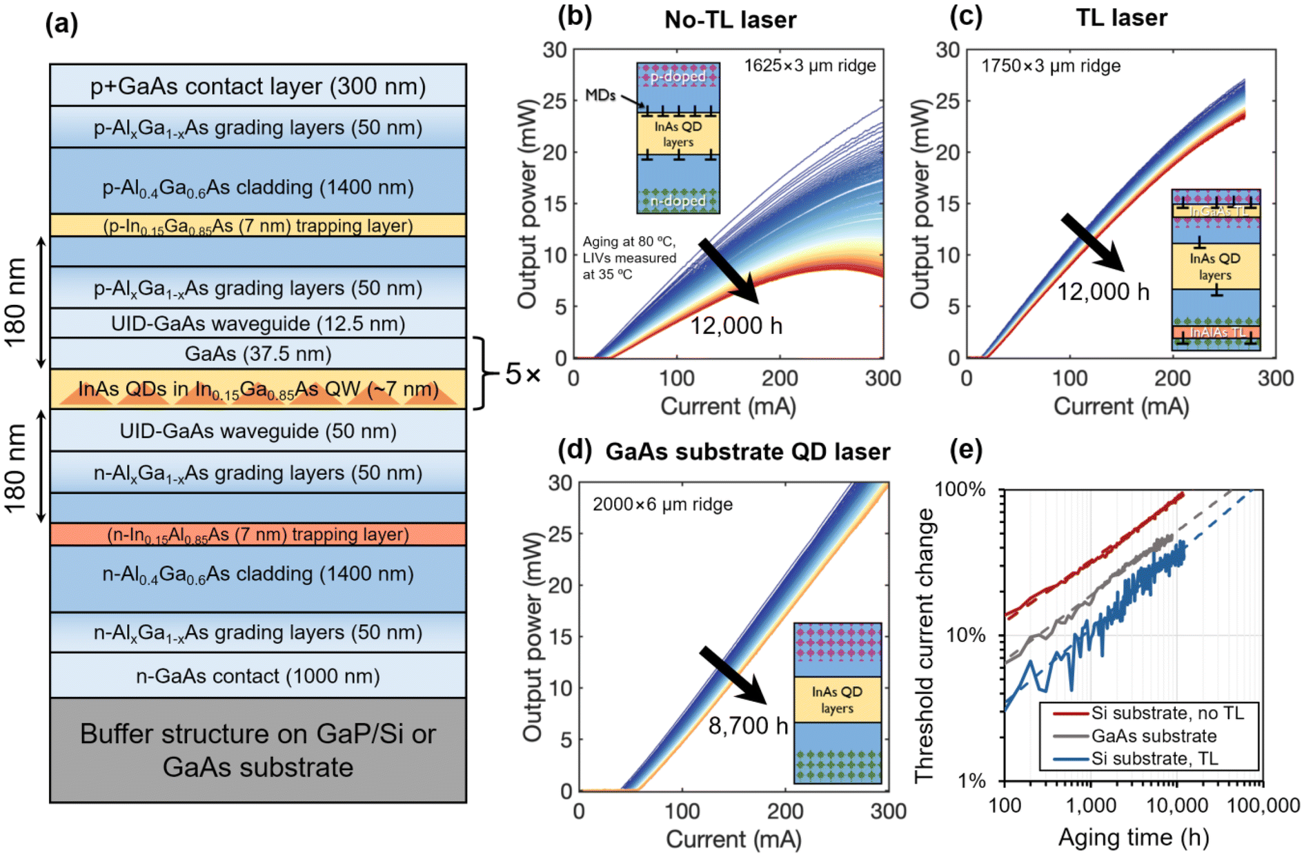 | ||
| Fig. 1 (a) Schematic of laser structure with trapping layers. (b–d) Light output vs. current (L–I) measurements over the course of aging for the three lasers: (b) on silicon without trapping layers (12000 h), (c) on silicon with trapping layers (12000 h), and (d) on GaAs substrate (8700 h). (e) Laser degradation rates measured by increase in threshold current. Extrapolated lifetimes (100% increase in threshold current) are indicated with the dashed lines. | ||
Unsurprisingly, the no-TL laser (Fig. 1b) performs worst. It doubles its 80 °C threshold current after just 2700 h and fails to lase entirely at 80 °C after 5700 h (see Fig. S1† for 80 °C L–I data). On the other hand, trapping layers significantly improve device lifetime on silicon (Fig. 1c) since they displace MDs that form on either side of the active region to the doped cladding layers, demonstrated previously.9,14,15 Nevertheless, both the TL laser (Fig. 1c) and GaAs substrate laser (Fig. 1d) undergo significant degradation with extrapolated lifetimes of 75000 h and 45000 h, respectively, shown in Fig. 1e. This degradation occurs despite them having far fewer (TL) or no (GaAs) grown-in MDs in the active region. We cannot yet claim that TL lasers on silicon are as reliable as GaAs substrate lasers from this data due to the different laser dimensions and aging conditions employed.
To determine the source of this degradation, the lasers were unmounted and their back surfaces cleaned to enable backside EL imaging. Fig. 2a–d shows EL from the aged no-TL and TL lasers and comparable unaged lasers imaged using an InGaAs camera (Hamamatsu). Both the aged and unaged devices show significant variation in intensity along their lengths primarily due to fabrication inhomogeneities and MDs near the active region (non-trapped) that are unrelated to aging. Both aged devices are much dimmer, however, with double the pump current required to produce comparably bright images. This is summarized in Fig. 2e where the equalized EL intensities averaged along the ridges are plotted, adjusting for different pump currents by assuming a linear relation with EL intensity. We caution against comparing intensities between the TL and no-TL sets, however, since differing substrate thickness and backside roughness changes the relative intensities.
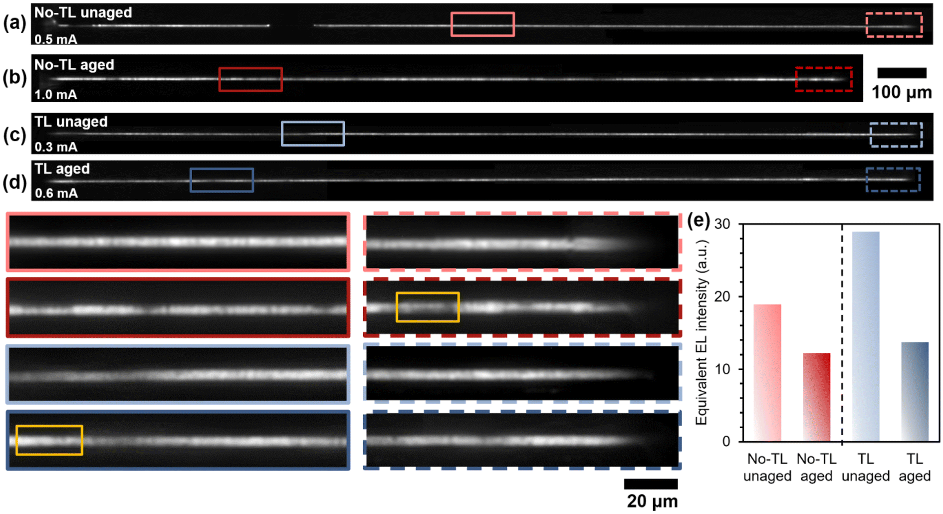 | ||
| Fig. 2 (a) Electroluminescence (EL) imaging of an unaged no-TL laser comparable in initial performance to the aged no-TL laser shown in (b). The long dark section in (a) is due to partially detached contact metal. The unaged and aged TL lasers are shown in (c) and (d), respectively. Pump current is adjusted to produce comparable brightness for each device. Magnified inset images along the ridge (solid boxes) show no notable change in density of dark line defects, but they do appear darker after aging. Degradation at the facet (dashed boxes) is negligible. Yellow solid boxes mark the regions extracted for TEM analysis. (e) Equivalent EL intensity, i.e. adjusted for pump current, averaged along each laser shows strong dimming of the aged devices. The dark segment in (a) is excluded from the averaging. | ||
Higher magnification EL insets in Fig. 2a–d (solid boxes) show similar densities of dark line defects for both aged and unaged devices but their contrast is stronger in the aged devices, indicating localized degradation at these defects. We note, though, that even regions unaffected by these defects are still significantly dimmer (after accounting for the higher pump current), i.e., the laser is also deteriorating homogenously. By comparing TL and GaAs laser aging behavior, it is this homogenous dimming component that appears to contribute more to degradation than the line defects, at least for the TL laser. The aged no-TL laser curiously appears only to have a slightly higher density of dark line defects than the aged TL laser, though with darker contrast due to the harsher aging condition. This may be misleading given the limited resolution of EL and the small 3 μm ridge width, which makes distinguishing dark line defects from dark spot defects difficult. Facet degradation appears negligible as evidenced by the magnified facet EL images in Fig. 2a–d (dashed box inset) with similar contrast profiles. No EL was collected from the aged GaAs laser due to a short circuit forming during post-aging processing, but an unaged neighboring device shows no dark line defects (i.e., no grown-in dislocations), so degradation is expected to be uniform.
Microstructural characterization
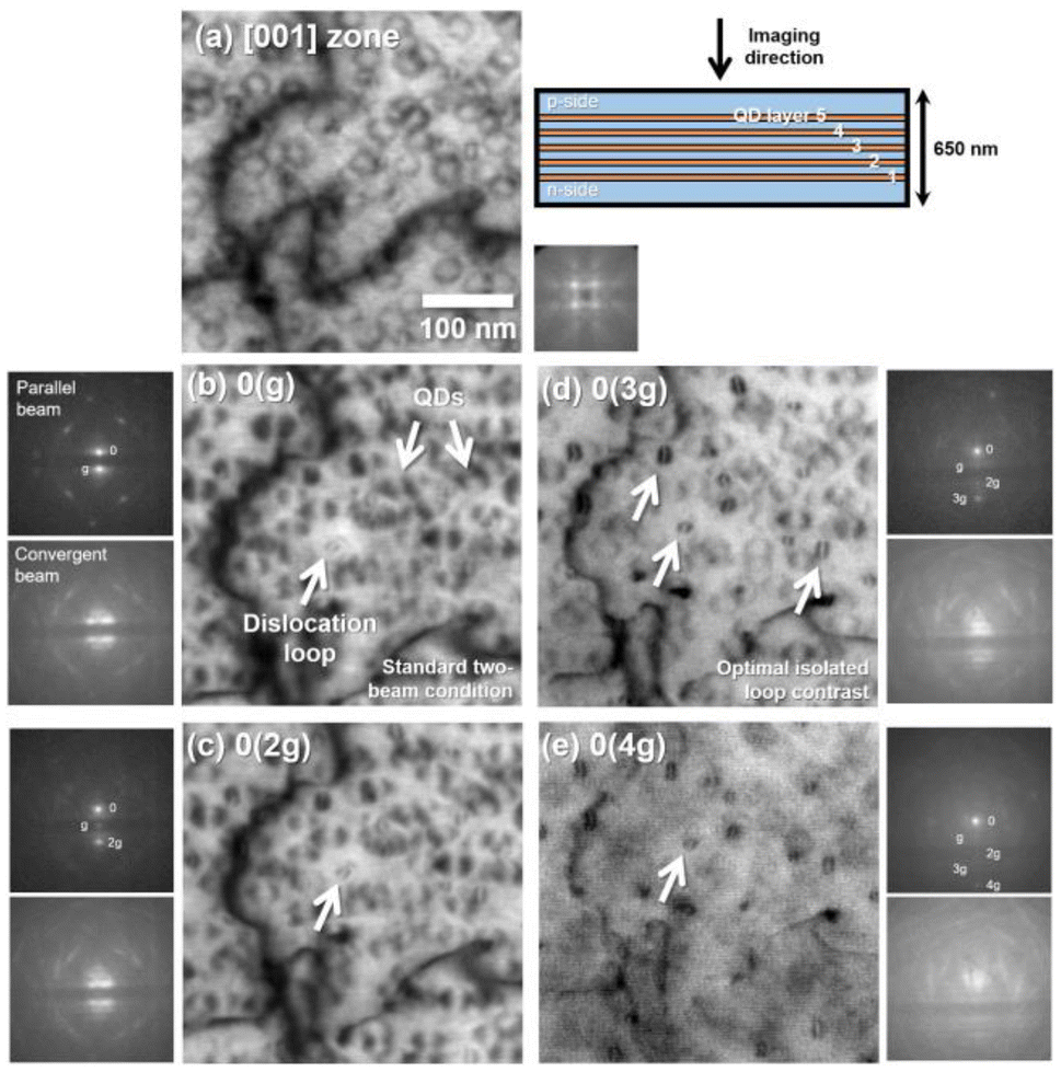
Plan-view foils were extracted from the aged lasers using standard focused ion beam techniques and imaged by STEM at 200 kV (ThermoFisher Scientific, Talos), shown in Fig. 3a–c. The extracted locations for the TL and no-TL lasers are marked with yellow boxes in Fig. 2b and d magnified insets. Serpentine MD segments result from previously straight dislocation segment undergoing recombination-enhanced dislocation climb by interaction with point defects.13 The extent of the meander away from the original position is directly related to the number of point defects involved, a point we will return to. The correspondence between the MDs in Fig. 3 and EL dark lines in Fig. 2 is not exact as there are many more MDs than dark lines. This can be explained by recognizing that the p-modulation doping of the active region shifts the depletion region toward the n side, which will reduce non-radiative recombination and hence EL contrast of MDs on the p side. MDs on the n side may also be more potent non-radiative recombination centers due to their core chemistry.22,23 For example, there is good correspondence between the dark horizontal line in EL that occupies most of the yellow box in Fig. 2b (no-TL inset) and the heavily climbed MD in Fig. 3a (yellow arrow), which is determined to be on the n side through tilt sequence imaging. While all MDs in the no-TL laser experience climb, only a small fraction of them do so in the TL laser (Fig. 3b, yellow arrows). No MDs or TDs were observed in the GaAs laser (Fig. 3c), as expected. In summary, MD climb is responsible for the degradation of the no-TL sample. However, the climb of pre-existing dislocations does not explain the gradual degradation observed in the TL laser nor, trivially, for the GaAs laser.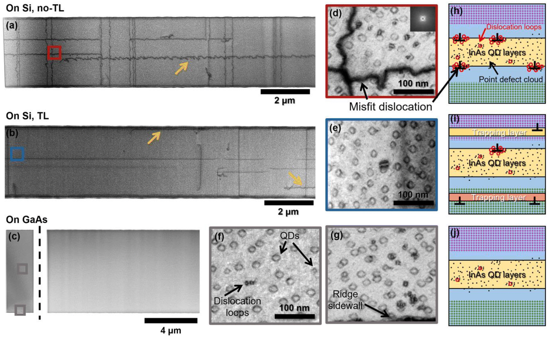 | ||
| Fig. 3 Plan-view scanning transmission electron microscopy (STEM) of the three aged lasers. (a) Section of the no-TL laser containing all 5 QD layers. (b) Section of the TL laser containing all QD layers and both TLs. Climbed dislocations, which have escaped the TLs, are marked with yellow arrows. (c) Section of the GaAs laser containing all QD layers (right) and a thinned section with adjusted contrast (left). After thinning, many dislocation loops are visible near the climbed MDs in the (d) no-TL laser, while the (e) TL laser and (f) GaAs lasers contain typically sparser dislocation loop populations. (g) An elevated loop density near the ridge sidewall. (h–j) Schematics of dislocation loops and the invisible point defects in the (h) no TL, (i) TL, and (j) GaAs laser. All images are collected in the [001] zone-axis condition. | ||
We look for clearer signatures of degradation in the microstructure by thinning each foil further, such that only 1–3 QD layers nearest the p-doped side remain. In Fig. 3d, we find a large population of dislocation loops in the no-TL laser ranging in size from 5 to 20 nm that cluster around certain regions of climbed MDs (up to 150 nm from the dislocation). The local dislocation loop density is approximately 1010 cm−2 near this dislocation. But looking widely, the correspondence between loop clusters and significantly climbed MD sections is tenuous. Loops are, however, about twice as common around heavily climbed MDs on the n-side of the laser compared to the moderately climbed p-side MDs. The TL and GaAs lasers, despite the partial or complete absence of dislocations near the active region, still contain dislocation loops, shown in Fig. 3e, f and g, respectively, with a density on the order of 108–109 cm−2 integrated over the active region thickness. The arrangement of MDs, dislocation loops and expected point defects for each device is shown schematically in Fig. 3h–j.
In the GaAs laser, dislocation loops are especially common within 50 nm of the edge of the deeply etched ridge. Fig. 3g shows an exceptional case of this where a heightened loop density extends over 300 nm from the sidewall, but the reason for this is not clear as the sidewall does not appear visibly different from other locations. This preferential loop formation near the sidewalls is not so apparent in the lasers on silicon due to an improved etching and passivation process. The loops in the GaAs laser are also notably smaller than in either laser on silicon, possibly a consequence of the shorter aging time.
We established that dislocation loops are closely associated with climbed MDs. These untrapped MDs lie just above the upper QD layer or just below the lower layer, but their associated loops preferentially form near the QD layer, rather that forming uniformly above and below the MD. This is demonstrated in Fig. 4. After thinning the no-TL sample just enough to begin removing the upper climbed MD, all loops near to that MD remain behind, indicating they sit lower in the sample. QDs might act as nucleation sites for loop formation, but while some loops appear to form directly over a QD, many others lie in the matrix in-between. We can additionally determine approximately where the loops lie in the vertical plane relative to the climbed MDs by imaging the no-TL sample across a range of tilt angles. Shown in Fig. S2,† all loops associated with climbed MDs remain near the plane of the MD. This may be because recombination enhanced diffusion24 is favored laterally through the quantum well that encases the QDs where carrier concentrations are highest. We have also observed loops unassociated with MDs that are distributed throughout the active region.
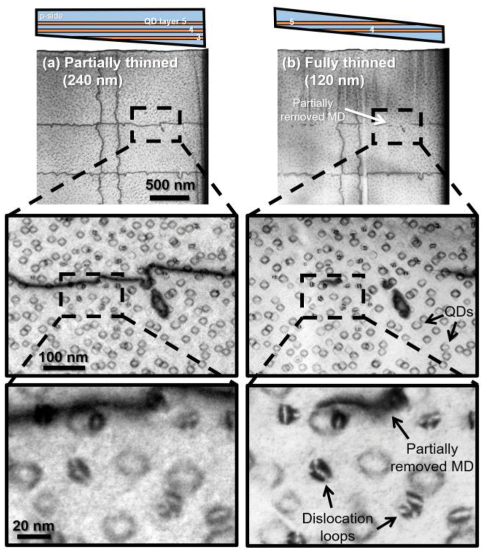 | ||
| Fig. 4 (a) [001]-zone plan-view BF STEM of the partially thinned sample from the no-TL laser. Magnified insets show a dislocation loop cluster near a climbed MD. The inset diagram above is a side profile showing approximately which of the five QD layers remain in the thinned sample. (b) The same sample thinned further to partially remove the MD on the p side of the laser, but not the QDs themselves. Notably, the dislocation loops that form near this MD all remain behind indicating the loops are centered not around the MD but around the QDs themselves. | ||
The dislocation loops have a similar appearance and orientation across all three aged samples and likely have a common structure. To determine their Burgers vector, we image the no-TL sample for its high loop density in several diffraction conditions to identify loop invisibility conditions. Dislocation loops in GaAs-based materials have either  or
or 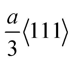 family of Burgers vectors, so we limit our search to these. Imaging with typical two-beam conditions (g = 220 or g = 400) gives strong quantum-dot contrast often with a similar appearance to dislocation loops, making invisibility determination difficult. To combat this, we image using higher-order diffraction vectors,25 3g220 (g = 660) and 2g400 (g = 800), which provide reasonably clear images of dislocation loops even, remarkably, through all five QD layers. Fig. 5 presents a systematic sweep over higher-order g220 diffraction vectors, demonstrating how the 3g220 condition preferentially isolates loop contrast from QD contrast without reducing image contrast too severely. The loop Burgers vector is determined in Fig. 6, where two dislocation loops are tracked across four diffraction conditions with a red and a yellow arrow. The translucent arrows in Fig. 5a and b indicate the loop is invisible. Both loops are visible in the two 2g400 conditions (Fig. 5c and d). Based on predicted invisibility (see Table S1†), this strongly suggests a Burgers vectors of
  type, i.e. a Frank dislocation loop. This assignment is reasonable since the loop diameter is still small and the well-known unfaulting reaction to form a perfect
 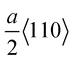 loop is not yet energetically favorable.26
 | ||
| Fig. 5 Comparison of BF STEM diffraction conditions on dislocation loop visibility and contrast. (a) On-zone imaging gives balanced contrast with dislocation loops only faintly visible amid the 5 QD layers. (b) Tilting to a standard g = 220 two-beam condition produces strong misfit-dislocation contrast and double-lobed QD contrast, making dislocation loops very difficult to see with their weaker contrast and smaller size. (c) Strongly exciting 2g220 slightly reduces QD contrast making dislocation loops more visible. (d) This trend continues for 3g220 where now dislocation loop contrast is relatively stronger than QD contrast. (e) In the 4g220 condition total contrast becomes very weak, though contrast separation is still further enhanced. This higher-order diffraction vector imaging technique is somewhat analogous to weak-beam dark field imaging in TEM, but STEM allows imaging through much thicker samples with less background contrast variation. For optimal contrast isolation, it is necessary to avoid exciting nearby diffraction conditions as much as possible since these strengthen QD contrast. Using the diffracted signal intensity for imaging gives comparable contrast isolation but with a much weaker signal. | ||
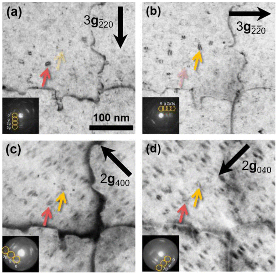 | ||
Fig. 6 Invisibility conditions for dislocation loops. (a) 3g220 and (b) 3g2![[2 with combining macron]](https://www.rsc.org/images/entities/char_0032_0304.gif) 0 images highlight two loops with alternating invisibility. In each, the translucent arrow indicates an invisible loop. In the (c) 2g400 and (d) 2g040 images, both loops are visible (dark arrows). 0 images highlight two loops with alternating invisibility. In each, the translucent arrow indicates an invisible loop. In the (c) 2g400 and (d) 2g040 images, both loops are visible (dark arrows). | ||
Discussion
Frank dislocations loops have been seen before in degraded GaAs-based LEDs and lasers. Ueda et al.20,27,28 use an inside-outside TEM contrast method and characterize these loops as having an interstitial character, i.e., they contain an additional set of {111} planes of both Ga and As atoms, preserving lattice polarity. Frank dislocation loops form by the coalescence of point defects. The Burgers vector is normal to the plane of the loop, and the loop grows laterally by climb, attaching atoms to the boundary of the additional plane. Ueda specifically notes such interstitial dislocation loops form not only randomly in the bulk of the device, but also in large numbers near climbed segments of pre-existing dislocations, similar to our observation for the no-TL sample and in previous work.13 While it is tempting to suggest that the dislocation loops must be a consequence of excess point defects generated from the climb of the pre-existing dislocations that precipitate out, it is noteworthy that pre-existing straight segments of dislocations (such as threading or misfit type with 60° character) in GaAs devices also climb by attaching atoms to the core.13,29 Thus, Ueda clearly sees a common driving force behind dislocation climb in GaAs, irrespective of whether the dislocation is in the form of a loop or a straight segment. We had previously suggested that the cluster of dislocation loops could be vacancy type in QD lasers due to excess vacancy generation following atom attachment to the MDs in the no-TL laser,13 however seeing them also in the TL and GaAs samples leads us to conclude similarly to Ueda et al. that they are likely of interstitial character in all samples. The dislocation loops in our samples are presently too small for unambiguous assignment via inside-outside contrast, particularly amid competing QD strain contrast. This does leave open the question of why dislocation loops cluster near climbing MDs in the no-TL sample.
Regardless of the exact nature of the point defects emitted or absorbed that form the loops, we find a net imbalance of point defects at dislocations of the no-TL sample. A conservative estimate of the local point defect density involved in dislocation climb in the vicinity of a climbed MD is 3 × 1019 cm−3. We can assess this from the area swept by the MD as it climbs and then assume that point defects necessary to accommodate this climb laterally diffuse a radius of 500 nm to or from the dislocation core but remain confined near the quantum well nearest to the MD. The density of point defects is greater if the diffusion length is shorter. The minimum point defect density needed to form the dislocation loops near the MD observed here is on the order of 1018 cm−2 (assuming a local loop density of 1010 cm−2, a 5–10 nm average loop diameter, and similar diffusion behavior as before). Thus, it appears that most of the point defects stay dissolved in the bulk and the visible dislocation loops are simply the tip of the iceberg in terms of nonradiative defects present. Experiments using deep-level transient spectroscopy (DLTS) indeed see an increase in electrical activity of point defects upon aging quantum well lasers, suggesting that point defects are generated during the experiment;20 however, there has not yet been a conclusive assignment to which defect is increasing in number.
To improve reliability, we suggest several strategies for future devices. First, changing the fabrication design from a deep-etch ridge to a shallow-etch ridge, where the active region remains unetched near the mesa, will improve initial performance by reducing non-radiative recombination at the sidewalls and removing crystal damage and the free surface, which can act as potent sources of point defects, as Fig. 3g demonstrates. Second, reducing the starting point defect density may be crucial to long lifetimes, so modifications to growth and to post-growth processing should be investigated, including post-growth annealing and potentially altering group-V/III flux ratios when growing QDs and the surrounding layers. These factors have been shown to strongly influence degradation rates of GaAs quantum well and double heterostructure lasers.30,31 Both these and QD lasers contain GaAs in or near the active region and may share a common degradation mechanism, so further optimization should benefit QD lasers. Recent collaborations have demonstrated, via DLTS measurements, that QD lasers on silicon and GaAs share a common hole trap associated with a native point defect species or an oxygen complex.32 Extending this experiment to test devices before and after aging can reveal whether this trap state multiplies over time and is the likely source of gradual degradation. Additional experiments link the rate of degradation to a diffusion limited process and find the dopant beryllium to be a likely candidate.33 Beryllium is present both in the p-doped cladding layers and in the thin p-modulation doped layers between each QD layer. Experiments are ongoing to replace beryllium with carbon, a less diffusive p-type dopant, and compare degradation rates. Others have recently demonstrated highly promising early reliability results from QD lasers similar to those discussed here.9 These lasers have three additional QD layers and a shallow rather than a deep-etch ridge. It is likely some of these differences or other unreported details such as growth parameters or dopant species contribute to the gap in reliability performance, so further gains are anticipated by addressing these point-defect-based degradation modes.
Finally, dark line defects are not entirely absent from the TL laser and further performance benefits should be available by optimizing trapping layer design to reduce the small fraction of MDs that escape the trapping layer and return to the active region.6,14 Parameters such as thickness, composition, spacing, and number of trapping layers are all relevant to trapping effectiveness. An initial study14 indicates that closer spacing improves this metric but has the drawback of closer MD proximity to the depletion region and possible slow climb of these dislocations. This may be avoided by using a thinner undoped waveguide layer or by growing multiple trapping layers to periodically reinforce TD pinning to simultaneously achieve high trapping layer effectiveness and larger MD spacing.
Conclusions
We show that gradual degradation in InAs quantum dot lasers is accompanied by the formation of dislocation loops, similar to what has previously been observed in conventional lasers with GaAs and AlGaAs double heterostructures and quantum wells. While the additional carrier confinement and strain fields of QDs slow these gradual degradation processes, they do not entirely halt them. The observed loops themselves are likely nonradiative recombination centers, but we believe the wider elevated background of point defects is the primary source of degradation. This degradation may be reduced by altering growth parameters and post-growth thermal processing, modifying laser fabrication design, and improving trapping layer performance. Further progress, however, requires a more fundamental understanding of these degradation mechanisms, which continued studies leveraging techniques such as DLTS to pinpoint the evolving point defect species can provide.Author contributions
Eamonn T. Hughes: conceptualization, investigation, methodology, visualization, writing – original draft, writing – review & editing. Chen Shang: investigation, resources. Jennifer Selvidge: investigation, methodology, writing – review & editing. Daehwan Jung: investigation, resources. Yating Wan: investigation, resources. Robert W. Herrick: supervision, writing – review & editing. John E. Bowers: funding acquisition, project administration, supervision. Kunal Mukherjee: methodology, supervision, writing – review & editing.Conflicts of interest
There are no conflicts to declare.Acknowledgements
This material is based on research sponsored by the Air Force Research Laboratory, under agreement number FA8650-21-2-1000. The U.S. Government is authorized to reproduce and distribute reprints for Governmental purposes notwithstanding any copyright notation thereon. The views and conclusions contained herein are those of the authors and should not be interpreted as necessarily representing the official policies or endorsements, either expressed or implied, of the Air Force Research Laboratory or the U.S. Government. TEM experiments were carried out at the UCSB MRL Shared Experimental Facilities, supported by the MRSEC Program of the NSF under Award No. DMR 2308708; a member of the NSF-funded Materials Research Facilities Network. The authors are grateful to O. Ueda for helpful discussions.References
- N. Margalit, C. Xiang, S. M. Bowers, A. Bjorlin, R. Blum and J. E. Bowers, Appl. Phys. Lett., 2021, 118, 220501 CrossRef CAS.
- J. Meng, M. Miscuglio, J. K. George, A. Babakhani and V. J. Sorger, Adv. Photonics Res., 2021, 2, 2000033 CrossRef.
- J. C. Norman, D. Jung, Y. Wan and J. E. Bowers, APL Photonics, 2018, 3, 030901 CrossRef.
- N. El-Masry, J. C. L. Tarn, T. P. Humphreys, N. Hamaguchi, N. H. Karam and S. M. Bedair, Appl. Phys. Lett., 1987, 51, 1608–1610 CrossRef CAS.
- C. Shang, J. Selvidge, E. Hughes, J. C. Norman, A. A. Taylor, A. C. Gossard, K. Mukherjee and J. E. Bowers, Phys. Status Solidi A, 2021, 218, 1–9 CrossRef.
- J. Selvidge, J. Norman, E. T. Hughes, C. Shang, D. Jung, A. A. Taylor, M. J. Kennedy, R. Herrick, J. E. Bowers and K. Mukherjee, Appl. Phys. Lett., 2020, 117, 122101 CrossRef CAS.
- I. Németh, B. Kunert, W. Stolz and K. Volz, J. Cryst. Growth, 2008, 310, 1595–1601 CrossRef.
- R. Alcotte, M. Martin, J. Moeyaert, R. Cipro, S. David, F. Bassani, F. Ducroquet, Y. Bogumilowicz, E. Sanchez, Z. Ye, X. Y. Bao, J. B. Pin and T. Baron, APL Mater., 2016, 4, 046101 CrossRef.
- Z. Xiangjie, L. Xiang, L. Guanlin, S. Ling, Z. Shiyong and Q. Haihua, 2023 Optical Fiber Communications Conference and Exhibition (OFC), DOI:10.23919/OFC49934.2023.10116887.
- A. Y. Liu, R. W. Herrick, O. Ueda, P. M. Petroff, A. C. Gossard and J. E. Bowers, IEEE J. Sel. Top. Quantum Electron., 2015, 21, 1900708 Search PubMed.
- Z. I. Kazi, P. Thilakan, T. Egawa, M. Umeno and T. Jimbo, Jpn. J. Appl. Phys., 2001, 40, 4903 CrossRef CAS.
- J. Selvidge, J. Norman, M. E. Salmon, E. T. Hughes, J. E. Bowers, R. Herrick and K. Mukherjee, Appl. Phys. Lett., 2019, 115, 131102 CrossRef.
- K. Mukherjee, J. Selvidge, D. Jung, J. Norman, A. A. Taylor, M. Salmon, A. Y. Liu, J. E. Bowers and R. W. Herrick, J. Appl. Phys., 2020, 128, 025703 CrossRef CAS.
- J. Selvidge, E. T. Hughes, J. C. Norman, C. Shang, M. J. Kennedy, M. Dumont, A. M. Netherton, Z. Zhang, R. W. Herrick, J. E. Bowers and K. Mukherjee, Appl. Phys. Lett., 2021, 118, 192101 CrossRef CAS.
- C. Shang, E. Hughes, Y. Wan, M. Dumont, R. Koscica, J. Selvidge, R. Herrick, A. C. Gossard, K. Mukherjee and J. E. Bowers, Optica, 2021, 8, 749 CrossRef.
- D. Jung, R. Herrick, J. Norman, K. Turnlund, C. Jan, K. Feng, A. C. Gossard and J. E. Bowers, Appl. Phys. Lett., 2018, 112, 153507 CrossRef.
- P. Petroff and R. L. Hartman, J. Appl. Phys., 1974, 45, 3899–3903 CrossRef CAS.
- H. Saito and T. Kawakami, IEEE J. Quantum Electron., 1977, 13, 564–567 CrossRef.
- M. J. Robertson, B. Wakefield and P. Hutchinson, J. Appl. Phys., 1981, 52, 4462–4466 CrossRef CAS.
- K. Kondo, O. Ueda, S. Isozumi, S. Yamakoshi, K. Akita and T. Kotani, IEEE Trans. Electron Devices, 1983, 30, 321–326 Search PubMed.
- J. H. Neethling, A. Janse Van Vuuren, E. J. Olivier and P. A. Van Aken, Acta Phys. Pol., A, 2019, 136, 245–249 CrossRef CAS.
- R. Jones, A. Umerski, P. Sitch, M. I. Heggie and S. Öberg, Phys. Status Solidi A, 1993, 137, 389–399 CrossRef CAS.
- C. Shang, E. T. Hughes, M. R. Begley, R. Koscica, M. Fouchier, K. Feng, W. He, Y. Wan, G. Leake, P. Ludewig and J. E. Bowers, Adv. Funct. Mater., 2023, 33, 2304645 CrossRef CAS.
- M. Uematsu and K. Wada, Appl. Phys. Lett., 1992, 60, 1612–1614 CrossRef CAS.
- P. J. Phillips, M. C. Brandes, M. J. Mills and M. de Graef, Ultramicroscopy, 2011, 111, 1483–1487 CrossRef CAS PubMed.
- D. Hull and D. J. Bacon, Introduction to Dislocations, Elsevier, Oxford, 5th edn, 2011 Search PubMed.
- O. Ueda, S. Isozumi, S. Yamakoshi and T. Kotani, J. Appl. Phys., 1979, 50, 765–772 CrossRef CAS.
- O. Ueda, Microelectron. Reliab., 1999, 39, 1839–1855 CrossRef.
- P. W. Hutchinson and P. S. Dobson, Philos. Mag., 1975, 32, 745–754 CrossRef CAS.
- T. Hayakawa, K. Takahashi, T. Suyama, M. Kondo, S. Yamamoto and T. Hijikata, Appl. Phys. Lett., 1988, 52, 252–254 CrossRef CAS.
- R. G. Waters, D. S. Hill, M. Douglas and A. Co, Influence of V/Ill Variation on AIxGal_xAS Quantum Well Lasers Grown by Metalorganic Chemical Vapor Deposition, 1988, vol. 17 Search PubMed.
- M. Zenari, M. Buffolo, C. De Santi, J. Norman, G. Meneghesso, J. E. Bowers, E. Zanoni and M. Meneghini, J. Phys. D: Appl. Phys., 2021, 54, 285101 CrossRef CAS.
- M. Buffolo, F. Lain, M. Zenari, C. De Santi, J. Norman, J. E. Bowers, R. W. Herrick, G. Meneghesso, E. Zanoni and M. Meneghini, IEEE J. Sel. Top. Quantum Electron., 2022, 28, 1–9 Search PubMed.
Footnote |
| † Electronic supplementary information (ESI) available. See DOI: https://doi.org/10.1039/d3nr05311c |
| This journal is © The Royal Society of Chemistry 2024 |