
 Open Access Article
 This Open Access Article is licensed under a
 Creative Commons Attribution 3.0 Unported Licence
Ultra-thin proton conducting carrier layers for scalable integration of atomically thin 2D materials with proton exchange polymers for next-generation PEMs†
Nicole K.
Moehring
 abc,
Andrew E.
Naclerio
b,
Pavan
Chaturvedi
bc,
Thomas
Knight
d and
Piran R.
Kidambi
*abce
abc,
Andrew E.
Naclerio
b,
Pavan
Chaturvedi
bc,
Thomas
Knight
d and
Piran R.
Kidambi
*abce
aInterdisciplinary Graduate Program in Materials Science, Vanderbilt University, Nashville, TN 37235, USA. E-mail: piran.kidambi@vanderbilt.edu
bChemical and Biomolecular Engineering Department, Vanderbilt University, Nashville, TN 37212, USA
cVanderbilt Institute of Nanoscale Science and Engineering, Nashville, TN 37212, USA
dDepartment of Chemistry, Vanderbilt University, Nashville, TN 37235, USA
eMechanical Engineering Department, Vanderbilt University, Nashville, TN, 37212, USA
First published on 14th February 2024
Abstract
Scalable approaches for synthesis and integration of proton selective atomically thin 2D materials with proton conducting polymers can enable next-generation proton exchange membranes (PEMs) with minimal crossover of reactants or undesired species while maintaining adequately high proton conductance for practical applications. Here, we systematically investigate facile and scalable approaches to interface monolayer graphene synthesized via scalable chemical vapor deposition (CVD) on Cu foil with the most widely used proton exchange polymer Nafion 211 (N211, ∼25 μm thick film) via (i) spin-coating a ∼700 nm thin Nafion carrier layer to transfer graphene (spin + scoop), (ii) casting a Nafion film and cold pressing (cold press), and (iii) hot pressing (hot press) while minimizing micron-scale defects to <0.3% area. Interfacing CVD graphene on Cu with N211 via cold press or hot press and subsequent removal of Cu via etching results in ∼50% lower areal proton conductance compared to membranes fabricated via the spin + scoop method. Notably, the areal proton conductance can be recovered by soaking the hot and cold press membranes in 0.1 M HCl, without significant damage to graphene. We rationalize our finding by the significantly smaller reservoir for cation uptake from Cu etching for the ∼700 nm thin carrier Nafion layer used for spin + scoop transfer compared to the ∼25 μm thick N211 film for hot and cold pressing. Finally, we demonstrate performance in H2 fuel cells with power densities of ∼0.23 W cm−2 and up to ∼41–54% reduction in H2 crossover for the N211|G|N211 sandwich membranes compared to the control N211|N211 indicating potential for our approach in enabling advanced PEMs for fuel cells, redox-flow batteries, isotope separations and beyond.
Introduction
The pristine lattice of atomically thin 2D materials such as graphene and hexagonal boron nitride (h-BN) allows for electric-field driven permeation of protons, while maintaining impermeability to atoms and larger ions.1–12 Such selective proton transport through 2D materials presents potential for enabling next-generation proton exchange membranes (PEMs) with minimal crossover of reactants or undesired species, thereby providing avenues to address persistent issues in conventional state-of-the-art proton conducting polymers e.g. Nafion.1–12Practical applications necessitate large area 2D material synthesis as well as facile integration approaches for realizing functional devices.13–20 In this context, chemical vapor deposition (CVD) has emerged as the most promising approach for large area 2D material synthesis.21–24 However, bottom-up synthesis via CVD inevitably introduces intrinsic defects into the 2D lattice.25,26 Intrinsic defects can enhance proton transport through 2D materials, but large intrinsic defects may also allow permeation of undesired species.11–15 Interfacing 2D materials with conventional state-of-the-art proton conducting polymers allows for synergistic advantages of reduced crossover (2D materials reduce crossover) while retaining high proton conductance (via intrinsic defects in 2D materials) by leveraging the low probability of large, non-selective defects in 2D materials aligning perfectly with pores/water channels of the Nafion support.10–12,27,28 Hence, the development of a facile and scalable approach to integrate 2D materials with Nafion is imperative.10–12,27,28
Hot pressing proton conducting polymers e.g. Nafion directly onto CVD graphene grown on Cu foil, has been explored in prior studies and optimized to enable large area graphene transfer for applications in fuel cell, redox flow batteries, isotope separations and beyond.2,7,11,29 However, oxidation of the Cu underneath defects in graphene can cause damage to graphene compromising selectivity, necessitating new approaches.29
Here, we systematically explore scalable approaches in addition to hot press to interface atomically thin CVD graphene with one of the most widely used PEM i.e. Nafion 211 (N211, ∼25 μm thick film). Specifically, we leverage casting a Nafion film on graphene on Cu foil followed by room-temperature pressing (cold press) to a N211 layer as well as a spin-coated ∼700 nm thin Nafion carrier layer (spin + scoop) to transfer graphene on N211 to minimize micron-scale defects to <0.3% area (∼88% less than conventional hot press transfer method). Graphene transfer via cold press or hot press results in ∼50% lower areal proton conductance compared to membranes fabricated via the spin + scoop method, but the areal proton conductance is recovered by soaking the membranes in 0.1 M HCl. We highlight the critical role of the significantly smaller reservoir for cation (Cu and ammonium ions) uptake from Cu etching2,11,30,31 for the ∼700 nm thin carrier Nafion layer used for spin + scoop transfer compared to the ∼25 μm thick N211 film for hot and cold press and demonstrate PEMs for H2 fuel cells with power densities ∼0.23 W cm−2 and up to ∼41–54% reduction in H2 crossover compared to bare Nafion control PEMs.
Experimental methods
Graphene synthesis and characterization
Graphene is synthesized via low pressure chemical vapor deposition (CVD) in a custom-built, 1′′ diameter tube furnace reactor.7,11,15–21,23,29,32 In brief, Cu foil (HA, 18 μm thickness, JX Holdings) is cleaned via sonication in ∼20% Nitric Acid followed by DI water wash and air drying.11 The Cu foil is heated to ∼1060 °C and annealed under 100 sccm H2 for 45 minutes, then 300 sccm for an additional 15 minutes.11 While maintaining a H2 flow rate of 300 sccm, the graphene growth is initiated by introducing methane via a two-step process to ensure a complete film: step 1 (0.5 sccm CH4 for 45 minutes), step 2 (1 sccm of CH4 for an additional 30 min).11 The system is quench cooled while still flowing the reaction gases until the temperature reaches <100 °C.Raman spectroscopy of graphene after transfer to 300![[thin space (1/6-em)]](https://www.rsc.org/images/entities/char_2009.gif) nm SiO2/Si (University Wafers) using poly(methyl) methacrylate (PMMA) carrier layer is used to determine the resulting graphene quality.7,11,32 2 wt% PMMA (Acros Organics, 35000 M.W.) in Anisole (BeanTown Chemical, 99%) is drop casted on the graphene on Cu foil, dried, then the Cu foil etched in 0.2 M ammonium persulfate (APS, Acros Organics, ACS reagent grade, (98+%)). Once fully etched, the graphene/PMMA stack is rinsed with DI water then scooped onto SiO2/Si wafers and dried before the PMMA is removed with acetone and rinsed with isopropanol. Raman spectra are collected using a Thermoscientific DXR Raman Microscope (532 nm, 1 mW laser, spot size ∼1.1 μm). For Raman of graphene already transferred to Nafion, the laser power was increased to 3 mW to improve the signal to noise ratio.
nm SiO2/Si (University Wafers) using poly(methyl) methacrylate (PMMA) carrier layer is used to determine the resulting graphene quality.7,11,32 2 wt% PMMA (Acros Organics, 35000 M.W.) in Anisole (BeanTown Chemical, 99%) is drop casted on the graphene on Cu foil, dried, then the Cu foil etched in 0.2 M ammonium persulfate (APS, Acros Organics, ACS reagent grade, (98+%)). Once fully etched, the graphene/PMMA stack is rinsed with DI water then scooped onto SiO2/Si wafers and dried before the PMMA is removed with acetone and rinsed with isopropanol. Raman spectra are collected using a Thermoscientific DXR Raman Microscope (532 nm, 1 mW laser, spot size ∼1.1 μm). For Raman of graphene already transferred to Nafion, the laser power was increased to 3 mW to improve the signal to noise ratio.
Proton exchange membrane (PEM) fabrication
Graphene is transferred to H+ form Nafion 211 (N211, 25 μm thickness, Ion Power) using three distinct methods (Fig. 1): (i) hot press, (ii) cast and cold press (referred to as cold press), and (iii) spin-coat and scoop (referred to as spin + scoop). Hot press: graphene on Cu foil is pressed to Nafion by sandwiching it between two sheets of PTFE-coated fiberglass sheets (McMaster Carr, ∼10 mil thickness) at ∼140 °C under 1000 psi for 3 minutes.7,11,29 Cold press: a thin layer of Nafion (1 wt% Nafion solution, 1100 EW – equivalent weight of Nafion in alcohol, Ion Power) is casted (via drop-casting or spin-coating) on CVD graphene on Cu before pressing N211 via sandwiching between the PTFE-coated fiberglass sheets at room temperature under 1000 psi for 3 minutes. Spin + scoop: Graphene on Cu foil is coated with a thin Nafion film via spin-coating. Three layers of Nafion are spin-coated (1000 rpm, 60 seconds) and dried to create a film strong enough to maintain structural integrity during the transfer process. The first layer consists of 5 wt% Nafion solution while the second 2 layers are 1 wt% Nafion solution. For each layer, ∼0.1 mL of Nafion solution is added and the sample spun for 60 seconds at 1000 RPM. Between each step, the film is dried at ∼60 °C for ∼10 minutes and a final drying time of ∼30 minutes. The resulting film thickness is ∼700 nm (see Fig. 1H).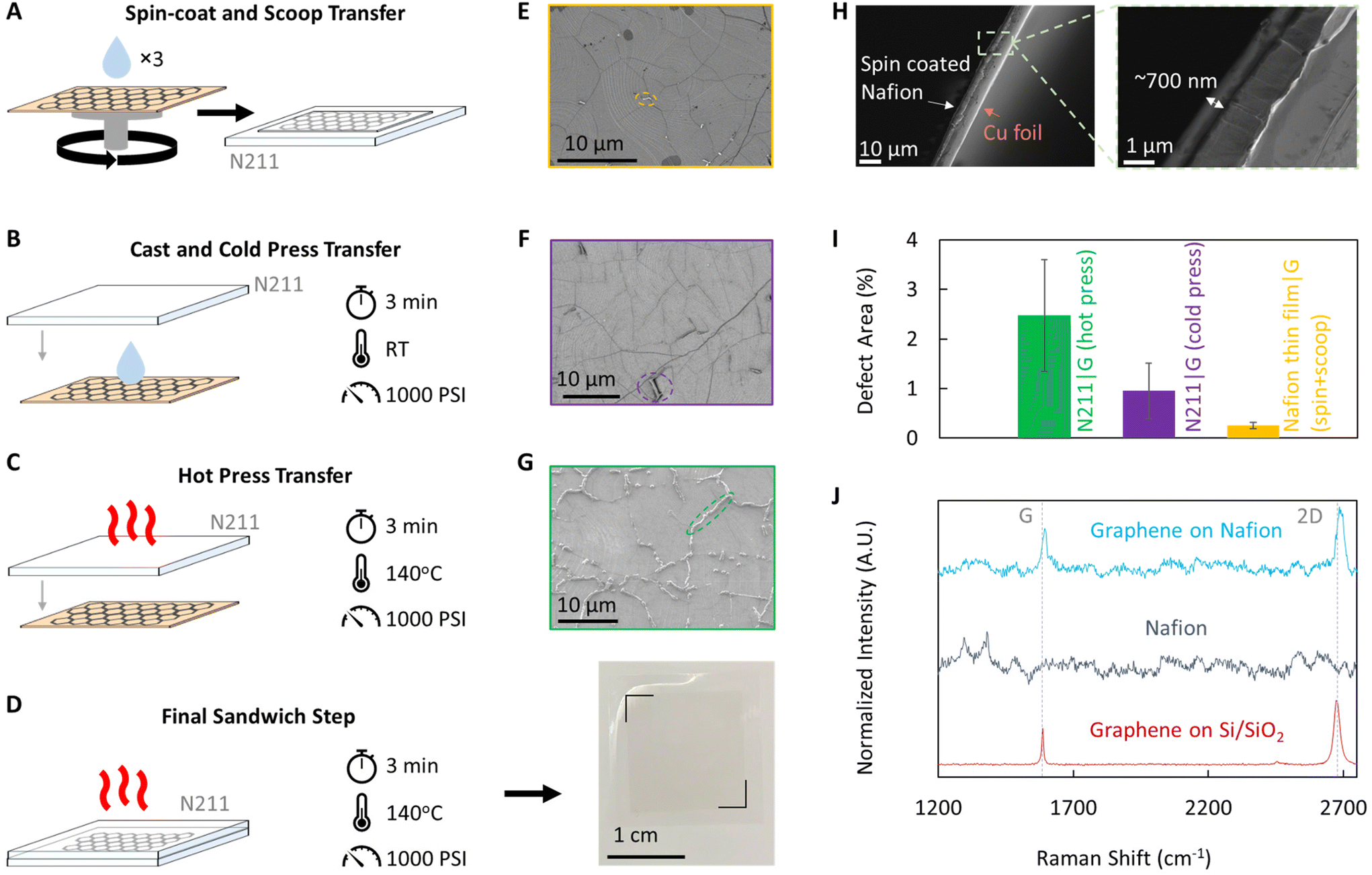 | ||
| Fig. 1 Graphene transfer and proton transport membrane (PEM) fabrication using spin + scoop, cold press, and hot press methods. Schematics of graphene transfer to 25 μm thick Nafion 211 (N211) using (A) spin-coat and scoop (referred to as spin + scoop), (B) cast and cold press (referred to as cold press), and (C) hot press methods. (D) Schematic of the final hot press step used to add the second N211 layer and optical image of the N211|G|N211 sandwich membrane. Black lines serve as guides to the eye and indicate graphene edges. Representative SEM images of graphene transferred to N211 via (E) spin + scoop, (F) cold press, and (G) hot press methods and (I) calculated percent defect area via image analysis using ImageJ software. Error bars represent one standard deviation. Common defects observed for each transfer method are circled. (H) Cross section SEM images of the spin + scoop Nafion layer coated on graphene on Cu foil, showing the thickness of the spin-coated Nafion layer is ∼700 nm. (J) Raman spectra for monolayer graphene transferred on to 300 nm SiO2/Si wafer (red curve) indicates high quality with the absence of a D-peak (∼1350 cm−1). The presence of G (∼1600 cm−1) and 2D (∼2700 cm−1) peaks in the Raman spectra of graphene transferred on to Nafion (light blue curve) in comparison to bare Nafion (dark blue curve) demonstrates successful transfer. | ||
Next, the Cu foil is etched using ammonium persulfate (APS) solution. An initial ∼10 min etch in 0.2 M APS, followed by ∼10 min float in DI water rinse is repeated twice to ensure that graphene on the bottom side of the Cu foil is removed before floating on ∼0.2 M APS for ∼3 hours to fully etch the Cu foil, after which the sample is rinsed in a series of DI water baths. For the hot press and cold press methods, the samples are dried, then the second layer of Nafion is added by hot pressing at 140 °C under 1000 PSI for 3 minutes to result in graphene sandwiched between 2 layers of N211. For the spin + scoop sample, a layer of Nafion attached to PTFE-coated fiberglass is submerged in the water and used to scoop the graphene|Nafion-thin-film stack onto it and then dried before adding the second Nafion layer via hot pressing.
Proton transport experiments
Proton transport characterization of the fabricated membranes were performed by supplying H2 gas as the source of protons and by adding ∼0.25-inch diameter platinum-carbon electrodes (Pt/C, 0.2 mg cm−2 Pt loading, Fuel cell store, ∼0.32 cm2) via hot press at ∼200 psi and ∼140 °C for ∼1 minute.7,11,29 Before testing, the membranes were soaked in DI water for 10 minutes to ensure the Nafion was fully hydrated (as prepared). Membranes were loaded into a custom-built miniature fuel cell and ∼40 sccm of humidified H2 gas (99.9999%, AL Gas) is introduced to both sides of the membrane (see Fig. 2A). A potentiostat (Gamry Interface 1010B) is used to run linear sweep voltammetry from −100 mV to +100 mV at a scan rate of 2 mV s−1. The membrane conductance is determined from the slope of the resulting curve:then normalized to the active area (∼0.32 cm2) to obtain areal proton conductance. After the initial proton conductance and H2 crossover measurements, the samples are removed from the measurement cell, soaked for 12 hours in 0.1 M HCl, rinsed in DI water and then reloaded in the cell and measured again (post acid soaking).
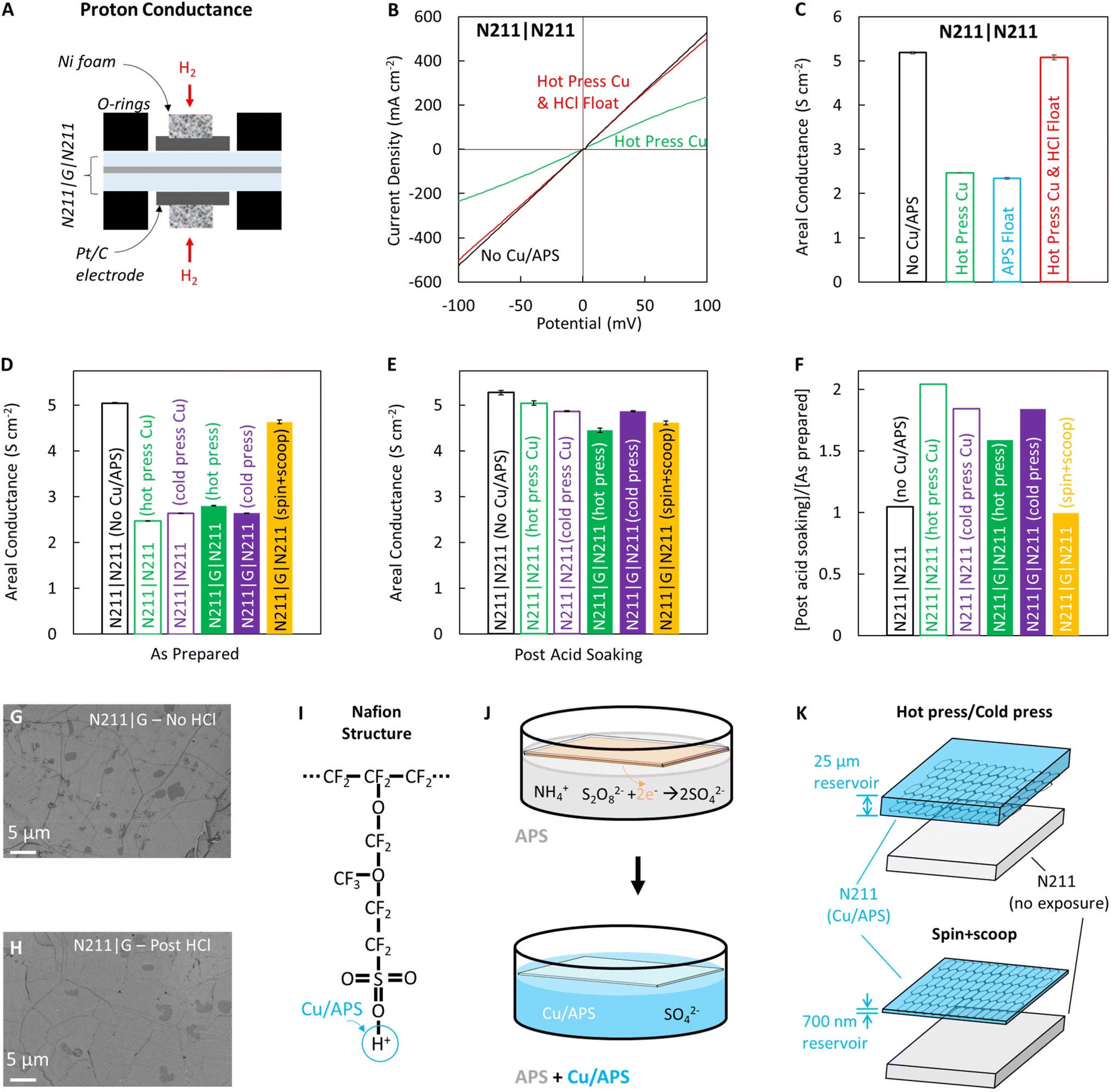 | ||
| Fig. 2 Areal proton conductance of N211|N211 and N211|G|N211 PEMs. (A) Schematic of cell and gas flow used for measurement of proton conductance. (B) I–V curves for Nafion sandwich membrane (N211|N211) without exposure to Cu or APS (No Cu/APS, black line), sandwich membrane which was pressed against bare Cu foil and etched in 0.2 M APS before (Hot press Cu, green line) and after soaking in 0.1 M HCl (Hot press Cu & HCl float, red line). (C) Areal conductance extracted from I–V curves in (C). An additional sandwich membrane where Nafion 211 was floated on APS solution (APS float, blue) without any Cu present, showing that ammonium ion contamination can also lead to conductance reduction. Areal conductance for N211|N211 (controls) and N211|G|N211 PEMs (D) as prepared and (E) after soaking in 0.1 M HCl. Note one of the N211|N211 control membranes was not exposed to Cu or APS solution [211|211 (no Cu/APS), black outline]. For all other membranes, Nafion is contacted with annealed bare Cu foil via hot press [211|211 (hot press Cu), green outline] or cold press [211|211 (cold press Cu), purple outline] or with graphene on Cu using hot press [211|G|211, green, filled], cold press (purple, filled), spin + scoop (yellow, filled) and the Cu is subsequently etched using 0.2 M ammonium persulfate (APS) solution. A reduced areal proton conductance is seen for all membranes (except the control not contacted with Cu or APS [N211|N211 (no Cu/APS)]. After soaking in 0.1 M HCl the proton conductance increases for all hot press and cold press membranes. Such a trend is not observed with the spin + scoop sandwich membrane as well as the N211|N211 (no Cu/APS) control membrane (black outline) and areal proton conductance remains relatively unchanged. (F) Ratios of proton conductance after soaking in 0.1 M HCl to conductance as prepared illustrate the change in areal proton conductance. Comparison of SEM images (G) before and (H) after soaking in HCl do not show an increase in cracks/tears (<3%) suggesting the acid soak increases areal proton conductivity without damaging the graphene significantly. Schematics of (I) exchange of ions in Nafion polymer chains, (J) the Cu etching process, and (K) the reservoir effect proposed to explain the observed change in areal proton conductance. Notably, the ∼700 nm thick Nafion film formed during the spin scoop process represents as significantly smaller reservoir for uptake of Cu or ammonium ions compared to the ∼25 μm thick Nafion 211 film. | ||
Ion exchange capacity (IEC)
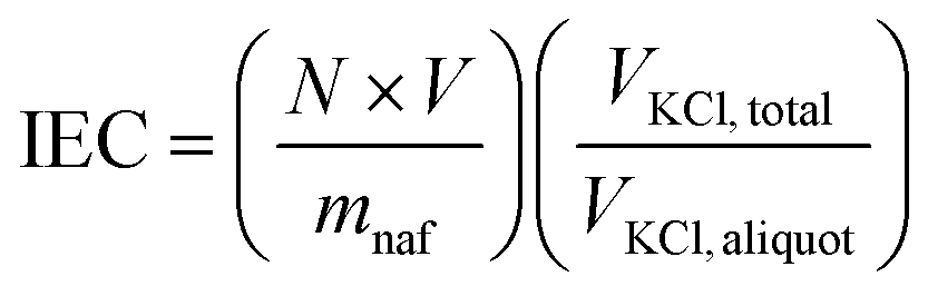
IEC was determined by neutralization titration.33 Membranes were prepared with Nafion 212 (N212, ∼50 μm thickness) using the hot press method. Prior to hot pressing, the N212 pieces were weighed to acquire their dry mass (mnaf). After sandwiching, each membrane is soaked in 75 ± 0.25 mL of ∼0.5 M KCl for ∼2 hours, then removed. Three aliquots of 20 ± 0.25 mL were taken and 2 drops of Brothymyl blue indicator (BTB) added to each so that a yellow color was observed. Each aliquot was titrated with ∼0.01 N NaOH until the aliquot color changed to green/blue, indicating a pH of ∼7.0. The IEC is calculated using:where N is the normality of the NaOH titrant, V is the volume of titrant added to neutralize the KCl solution, mnaf is the mass of the dry Nafion, VKCl, total is the total KCl volume the sample was soaked in, and VKCl, aliquot is the volume of each KCl aliquot.
Energy dispersive X-ray spectroscopy (EDS)
As prepared graphene transferred to N211 (N211|G) via hot press method was mounted to the sample holder (without soaking in 0.1 M HCl) and loaded into a Zeiss Merlin SEM with EDS. At a working distance of ∼8.5 mm, the N211|G sample is brought into focus at low magnification (<800×) to mitigate charging/damage to the sample due to the high voltages (20 kV) and probe current (2 nA) used. The EDS spectra was collected over ∼5 minutes in an area of the sample covered with graphene. Next, the magnification was increased (>800×) and the EDS spectra collected again.H2 crossover measurements
H2 crossover at room temperature is determined using electrochemical techniques previously described.7,11,12,29 ∼40 sccm of humidified H2 gas is flowed on one side of the membrane while ∼40 sccm of humidified N2 (99.999%, AL Gas) is flowed on the other side of the membrane and the OCV monitored until stable. Linear sweep voltammetry is run from +600 mV to −150 mV. At potentials above the OCV, the current results from hydrogen which diffused through the membrane and is available to react at the electrode on the N2 side of the membrane. Therefore, the measured current is directly related to the magnitude of H2 crossover through the membrane. The limiting current density at 400 mV is taken to compare crossover between membranes as per U.S. Department of Energy standard.11Hydrogen fuel cell
Fuel cell measurements were done at room temperature by supplying humified H2 to one side and humidified air to the other side of the membrane. An initial break-in procedure is performed prior to each measurement wherein the membrane potential is cycled between 600 and 200 mV, holding for 60 seconds at each step for ∼3 hours. I–V curves and power density plots are obtained by sweeping the applied potential from ∼900 mV to ∼200 mV at a scan rate of ∼2 mV s−1. Power density is calculated by multiplying current density by the potential. Maximum power density is extracted from the power density plots as the maximum point.Results and discussion
Transfer of CVD graphene to N211 via hot press, cold press, and spin + scoop approaches
Three different methods were used to transfer CVD graphene to N211: (i) spin-coating a thin layer of Nafion on CVD graphene on Cu, followed by subsequent etch of Cu and scooping the Nafion|graphene (N211|G) on to N211 (spin + scoop, Fig. 1A), (ii) casting a Nafion film on CVD graphene on Cu and cold pressing on to N211 (Fig. 1B) and subsequent etch of Cu, and (iii) hot pressing N211 on to CVD graphene on Cu and subsequent etch of Cu (Fig. 1C). Finally, another layer of N211 is hot pressed to fabricate an N211|G|N211 sandwich PEM, electrically isolating and protecting the graphene layer in-between (Fig. 1D).Scanning electron microscopy (SEM, Fig. 1E–G), and Raman spectroscopy (Fig. 1J) performed on graphene transferred to N211 (prior to hot pressing the additional sheet of N211) confirms successful graphene transfer. SEM images show wrinkles in graphene and some multi-layer spots indicating CVD graphene transfer using each method (Fig. 1E–G). Raman spectroscopy confirms (i) the high quality of the as-synthesized monolayer CVD graphene (Fig. 1J, red spectrum) as well as (ii) the successful transfer of graphene to Nafion (Fig. 1J, light blue spectrum, Fig. S1†). Raman spectra are collected from 1200 cm−1 to 2800 cm−1 as the characteristic graphene peaks appear within this range and allows confirmation of graphene transfer.10,34,35 Specifically, Raman peaks at ∼2690 cm−1 (2D), ∼1580 cm−1 (G), and the absence of a peak at ∼1350 cm−1 are characteristic to graphene and a ratio of ID/IG ∼0.032, confirms high quality (Fig. 1J, red spectrum).35,36 Nafion does not have peaks at 2690 cm−1 or 1580 cm−1 (Fig. 1J, dark blue spectrum).37 Hence, the presence of characteristic graphene peaks after graphene transfer is indicative of successful graphene transfer (Fig. 1J, light blue spectrum). However, broad, characteristic Nafion peaks are present around 1350 cm−1 (∼1300 cm−1 and 1380 cm−1) and therefore this method cannot be used to quantify the quality of the graphene after transfer to Nafion.
Notably, graphene transferred via hot press shows spot/linear defects (Fig. 1G) consistent with prior literature reports of damage to graphene via oxidation of the Cu foil underneath intrinsic defects in CVD graphene which are large enough to allow for H2/O2 permeation.29,38,39 Further, such oxidation related features appear to line up along wrinkles in CVD graphene,29,38,39 as is apparent when comparing CVD graphene on Cu foil that has been oxidized via heating in ambient atmosphere (see Fig. S2†).
Interestingly, graphene transferred without using elevated temperatures (as used in hot press) does not show oxidation related features (Fig. 1E and F). However, some minor areas with different damaged/ruptured regions for the graphene transferred via cold press are observed. These regions appear brighter under SEM imaging due to charging of the underlying exposed Nafion (due to the non-conducting nature of the polymer compared to graphene) along with much darker regions in the immediate vicinity (Fig. 1F). We attribute these darker patches to >1 layer of graphene that ruptured due to poor contact with the N211 (exposing Nafion in the bright regions of SEM) and folded over.29 We note that cold press in some instances results in large areas of non-conformal contact (see Fig. S3†) in addition to the minor ruptures, although they occurred less frequently across several samples we tested and were mitigated when a thin layer of Nafion is cast on the Cu|G before the cold press to N211 (Fig. 1B). Finally, we note that graphene transferred via a spin-coated, ultra-thin Nafion film (∼700 nm thickness, Fig. 1H) showed minimal damage/rupture of either type (Fig. 1E). A quantitative analysis of the percentage area attributed to defects/damage/ruptures (Fig. 1I) from SEM images with ImageJ confirms the qualitative observations with hot press > (∼2.5 ± 1.3%) > cold press (∼0.95 ± 0.56%) > spin + scoop (∼0.25 ± 0.07%) (Fig. 1I). We attribute the low defective area for the spin + scoop sample to the lack of elevated temperatures which ensures no damage results from the Cu oxidation and the spin-coated Nafion film achieving conformal contact with CVD graphene on Cu.
Areal proton conductance of the fabricated N211|G|N211 PEMs
Proton transport through fabricated PEM sandwich membranes was evaluated by adding Pt/C electrodes to either side of the membrane (0.32 cm2) and using a custom built, miniature test cell (Fig. 2A).11,29 The PEM is loaded into the cell and sealed between two graphite rods and Ni foam for electrical contact with Pt/C electrodes on either side and o-rings to isolate either side of the membrane from gas leakage. Current–Voltage (I–V) curves are measured while supplying humidified H2 gas on either side of the PEM (symmetric measurements), and the slope of the I–V curve collected using linear sweep voltammetry (LSV) is used to compute PEM conductance (Fig. 2B) using Ohm's law.11,29,34We note that CVD graphene transfer to N211 inevitably necessitates the removal of catalytic CVD substrate and chemical etching of Cu has emerged as the most preferred route due to Cu being relatively inexpensive, and since approaches such as mechanical peeling or interface oxidation for delamination can result in damage to CVD graphene.32,40 Hence, understanding the impact of this chemical etching process of Cu is imperative for facile and scalable PEM fabrication.
To evaluate the influence of the etching step on proton conductance, we prepare and study four different kinds of N211 (controls): (i) as received N211 with no exposure to Cu or etching solution of ammonium persulfate (APS), (ii) N211 hot pressed to bare Cu foil and etched in APS, (iii) N211 floated on fresh APS solution, and (iv) N211 hot press to bare Cu foil, etch in APS, then soaked in 0.1 M HCl (Fig. 2C). We subsequently sandwich each of these N211 layers with another as-received N211 (without any treatment) and proceed to evaluate proton transport through the N211|N211 PEMs.
The un-treated N211 shows the highest conductance ∼5.2 S cm−2 (Fig. 2C) but after exposure to Cu and APS, the conductance drops significantly ∼2.3–2.5 S cm−2. We hypothesize this lowering in areal conductance stems from uptake of cations present in the etching solution e.g. Cu and ammonium ions into Nafion replacing/exchanging the H+ usually present on the sulfonated groups (Fig. 2I).41,42 To test this hypothesis we soak the N211|N211 PEMs exposed to Cu and APS in dilute HCl (0.1 M) and find the areal conductance recovers to match that of the untreated membrane ∼5.1 S cm−2, suggesting that the cations have been exchanged out with H+ and contamination effectively removed. Similarly, we observe a drop in areal proton conductance to ∼2.5–2.6 S cm−2 for N211|N211 PEMs which were contacted with bare Cu via hot pressing and cold pressing (Fig. 2D) techniques in comparison to N211|N211 (no contact with Cu/APS) and recovery upon soaking in 0.1 M HCl (Fig. 2E). These observations are consistent with studies by Hongsirikarn et al.42 wherein the in-plane ionic conductance of N211 decreased linearly from ∼115 mS cm−1 to ∼25 mS cm−1 when equilibrated with increasing concentrations of ammonium ions via contamination of Nafion with NH4+ as well as re-protonation of Nafion via uptake cations present in solutions (acids with high H+ concentration) via diffusion.2,11
Hot as well as cold pressed graphene membranes N211|G|N211 also show lowering of areal proton conductance and recovery upon soaking in 0.1 M HCl, similar to the N211|N211 (controls) but the resistance of the graphene membrane remains higher than the controls (Fig. 2D–F), since graphene presents additional resistance to proton transport.2,11 Comparison of the areal conductance after soaking in 0.1 M HCl to the areal conductance as prepared, the control membranes demonstrate the greatest increase in conductivity (∼2×) while the hot press graphene sample changes by ∼1.5× and the cold press ∼1.8× (Fig. 2F). To ensure that the 0.1 M HCl soak is not introducing microscale defects, we imaged the graphene surface on Nafion within the same area via SEM before and after soaking in 0.1 M HCl and did not observe significant differences in the graphene features or the introduction of tears/ruptures (Fig. 2G and H). Interestingly, the spin + scoop sample did not show a significant drop in the proton conductance prior to acid soaking and upon acid soaking the proton conductance only marginally changes i.e. post acid soaking:as prepared ratio ∼0.99× (Fig. 2F). We propose these differences between spin + scoop vs. hot/cold pressed N211|G|211 PEMs originate from a reservoir effect (Fig. 2J and K) as well as any material properties differences for the ultra-thin ∼700 nm Nafion films versus ∼25 μm N211.
Nafion films have been suggested to experience confinement effects and substrate/film interactions with slower water diffusion and reduced water uptake, amongst other effects.43–46 Specifically, when casted on a hydrophobic surface, thin Nafion films have been suggested to orient the ionic domains parallel to the surface which in turn could reduce water uptake.43–46 For Cu and ammonium ions to exchange with the protons in the Nafion film, water must permeate through the graphene barrier via defects overlapping with the Nafion channels. Once there is water in the ionic channels, diffusion and ion exchange of Cu and ammonium ions with H+ can occur. Additionally, the N211 thickness is significantly greater than that of the spin-coated film (25 μm vs. 700 nm) and so the N211 has a greater volume for holding these contaminants, hindering efficient proton transport and reducing the conductance if not re-protonated (Fig. 2K). Hence, we conclude that when graphene is transferred to N211 via hot press or cold press, soaking in 0.1 M HCl is necessary to re-protonate and remove contamination from the etching step (i.e. Cu and ammonium ions), while graphene that is transferred via the spin + scoop method does not require an additional 0.1 M HCl soaking step.
Differences in the ion exchange capacity (IEC, mol of cation per g of Nafion) are also observed for graphene membranes which have contact with Cu2+ and NH4+ as compared to pristine Nafion (Fig. 3). Typically, Nafion in H+ form (i.e. protons associated with the sulfonate groups in the Nafion) can be exchanged out with other cations (K+) by soaking in a solution such as KCl. Due to the concentration gradient, the protons in Nafion diffuse into the KCl solution and are replaced with K+. The concentration of protons removed from the Nafion can then be determined by simple titration and the IEC value calculated. We note that although the addition of graphene has been shown to provide resistance to electrically driven K+ transport in Nafion, we do not expect the presence of graphene to completely eliminate the diffusion of K+ into Nafion during these experiments. Previous experiments with Nafion|G|Nafion membranes have indeed demonstrated that K+ can be fully removed from N211|G|N211 sandwich membranes by soaking in HCl.7,11
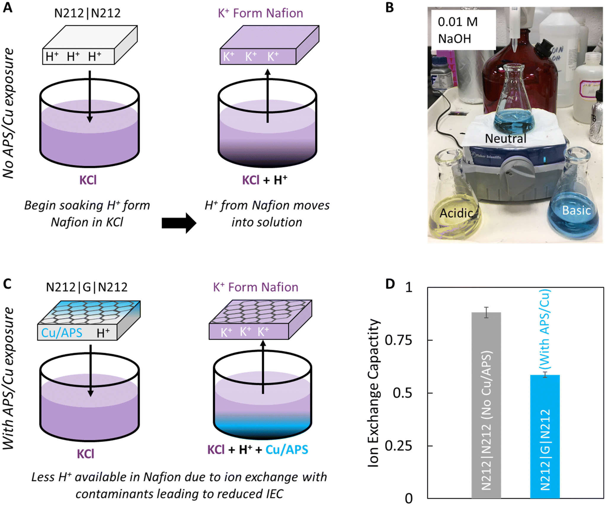 | ||
| Fig. 3 Ion exchange capacity (IEC) for membranes with and without exposure to Cu and ammonium persulfate (APS). (A) Schematic of IEC experimental method wherein an H+ form Nafion sandwich (N212|N212) is soaked in 0.1 M KCl solution and the H+ in the membrane is replaced with K+ from solution, thereby decreasing the pH. The concentration of H+ in solution (from the Nafion) is determined by titration and used to determine IEC. (B) Image of the aliquots of KCl solution after Nafion soaking at different stages of the titration process. When Brothymal blue (BTB) is added to the aliquot, the color starts as yellow (acidic). Once neutralized with 0.01 M NaOH, the solution turns to teal. Additional NaOH will make the solution light blue (basic). The volume of NaOH to neutralize the solution is used in the IEC calculation (see methods). (C) Schematic showing the same experimental method for IEC determination but after graphene has been added (N212|G|N212), which introduces contamination from the etching process (Cu and ammonium ions) and displaces a fraction of H+. (D) The calculated IEC for Nafion control membrane [212|212 (no Cu/APS, gray bar)] compared to the graphene membrane [N212|G|N212 (with Cu/APS)]. The lower IEC for the graphene membrane is confirmation of contamination/ion exchange in the Nafion during the etching process. | ||
The control sandwich membrane not exposed to Cu or APS has an IEC of ∼0.88 (Fig. 3D, gray bar). Slight deviation from the theoretical value of ∼0.9 could be attributed to the accuracy of the titration method or some variability in the mass of the dry Nafion due to residual water.33 When graphene is transferred to the Nafion (i.e. 1 layer of Nafion is exposed to Cu and APS), the IEC is significantly lower at ∼0.59 (Fig. 3D, blue bar). We attribute this low IEC to the reduced proton concentration in the Nafion due to the exchange with Cu and/or ammonia ions during the etching process. When soaked in KCl, these ions may still exchange out with the K+ but they do not contribute significantly to the acidity of the KCl solution to be titrated, thereby reducing the volume of titrant needed for neutralization and the subsequent calculated IEC.
To confirm whether Cu ions are participating in the ion exchange process with Nafion, we performed energy-dispersive X-ray spectroscopy (EDS) of a N211|G membrane (Fig. S4†) and observe the Cu Lα peak at ∼0.930 keV when we probe the sample surface, indicating the presence of Cu. At higher magnification (same beam energy distributed over a smaller area), the incident electron beam interacts with the Nafion sample, leading to deformation of the sample surface,47 and an emergence of the Cu Kα peak at ∼8.04 keV (Fig. S4B,† inset).
Hydrogen crossover and H2/Air fuel cell performance of the fabricated N211|G|N211 PEMs
Having developed approaches to effectively integrate graphene with Nafion and fabricate PEMs, we proceed to evaluate H2 crossover and H2/Air fuel cell performance of the fabricated N211|G|N211 PEMs (Fig. 4A and B and Experimental methods).11,48,49 We emphasize that since graphene is sandwiched between 2 layers of Nafion (N211), we cannot use direct imaging techniques to evaluate the morphology/surface chemistry of graphene and hence use H2 crossover reduction as a measure of the integrity of graphene and its barrier properties. For H2 crossover, I–V curves are obtained from LSV when flowing H2 on one side of the membrane and N2 on the other side of the membrane at equal mass flow rates (Fig. 4C). At potentials more negative than the open circuit potential (∼120 mV), we see the onset of the hydrogen evolution reaction, identified by the steep slope. At potentials more positive than the open circuit potential (H2 crossover region), the measured current results from the oxidation of H2 which has diffused as molecular H2 through the PEM.49,50 The crossover current density is taken at 400 mV for each membrane to compare relative crossover (Fig. 4D).49,50 As with the proton conductance, after HCl soaking the H2 crossover current densities for the controls whether pressed against bare Cu or not are similar at ∼0.32 mA cm−2 (Fig. 4D). Upon the incorporation of graphene, the crossover current densities for each of the graphene membranes (N211|G|N211) drops significantly as compared to the controls (N211|N211).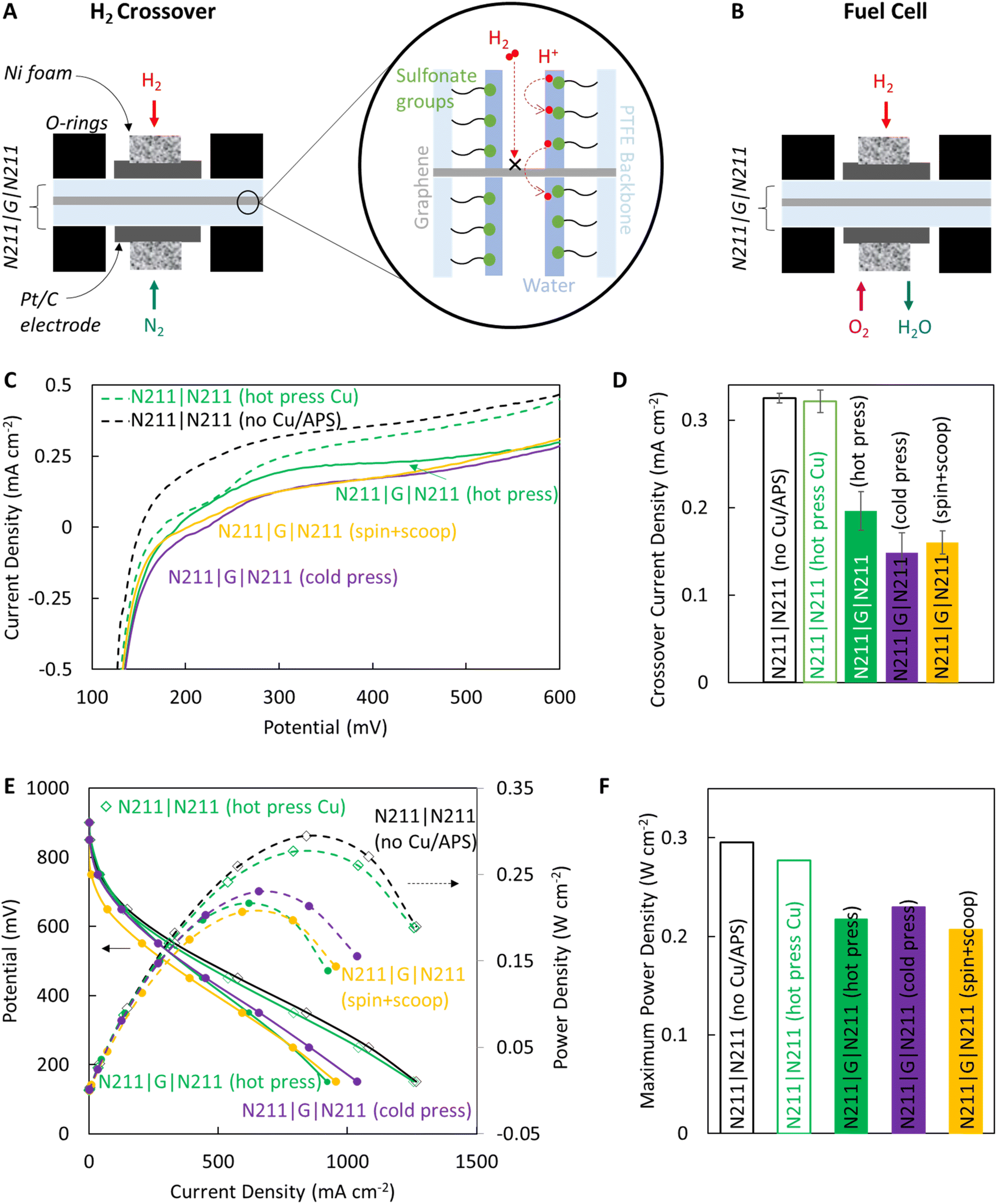 | ||
| Fig. 4 Performance of PEMs in fuel cells. Schematic of experiments for (A) H2 crossover and (B) H2:Air fuel cell performance. The N211|G|N211 sandwich is sealed in the cell with rubber o-rings and electrical contact made with the Pt/C electrodes and Ni foam. The graphene acts as a barrier between the Nafion layers, limiting H2 crossover but permeating protons and allow functionality in a fuel cell. (C) H2 crossover curves for the fabricated membranes shows reduction upon incorporation of graphene into the PEMs. (D) The H2 crossover current density for each membrane is determined from the current density at 400 mV. The reduction in H2 crossover is comparable to previous reports of H2 crossover reduction with single layer graphene.11 (E) Polarization I-V curves (left axis, solid lines) and power density curves (right axis, dotted lines) for each membrane in a custom-built H2/Air fuel cell. (F) Maximum power density for each membrane extracted from C. Moderate drops in power density are observed upon the addition of graphene. | ||
The hot press sample shows the lowest reduction in H2 crossover ∼41% (∼0.20 mA cm−2), in agreement with prior reports of crossover reduction (∼0.17 mA cm−2).11 The cold press and spin + scoop samples show higher H2 crossover reduction to ∼54% (∼0.15 mA cm−2) and ∼53% (∼0.16 mA cm−2), respectively. We also compare N211|G|N211 membranes to a single layer of N211, which is more commonly used than the sandwich structure in standard H2 fuel cells, and observe ∼87% reduction in H2 crossover (see Fig. S5†). We note that the gas phase measurements are done under humid conditions, which has previously been shown to result in lateral expansion of Nafion of up to ∼10% at room temperature.51 While this could cause strain in the graphene, it still allows for between 41–54% reduction in crossover. Reduced H2 crossover upon the addition of graphene can aid longevity of PEMs since reactant crossover (H2 and O2) reduces fuel cell efficiency and direct reaction between H2 and O2 can lead to the formation of peroxides which degrade Nafion, ultimately leading to membrane failure.49,50
We further evaluate beginning of life performance when the N2 feed is changed to air i.e. in an H2/Air fuel cell (Fig. 4B). Fuel cell measurements were done at room temperature in the same test fixture as the symmetric and asymmetric tests. Due to the significant drop in conductance observed for hot press and cold press samples prior to soaking in HCl, fuel cell measurements were only performed post acid soaking. During room temperature operation of the custom-built H2/Air fuel at atmospheric pressure, we found the performance of the membranes to be stable for the duration of the experiments (Fig. S6†). The graphene membranes demonstrate slightly lower max current densities (∼954–1004 mA cm−2) compared to the sandwich control membranes (∼1260 mA cm−2) as also reflected in the maximum power density (Fig. 4E and F). Between the hot press, cold press, and spin + scoop samples, max power density for the cold press sample is marginally higher than the hot press and spin scoop samples, which is consistent with the higher proton conductance measured for the cold press sample (Fig. 2 and Fig. 4D) but overall all membranes are impacted by the increase in ohmic resistance due to graphene. However, the max power density is only reduced by ∼22% while the H2 crossover is reduced ∼41–53%, indicating the graphene barrier successfully passes the typical selectivity/permeability tradeoff.
These beginning of life H2 fuel cell measurements serve as proof-of-concept experiments that the approaches developed for interfacing graphene with Nafion can be used for applications. The mitigation of deleterious effects from transfer processes allows future studies to focus on evaluating/optimizing fuel cell performance at elevated temperatures (∼70–80 °C) to increase efficiencies, extended time studies, stress testing, among others that could provide more technological insights into the role of the interfaced 2D material.
Conclusions
Scalable approaches to integrate proton selective atomically thin graphene with Nafion can allow for the development of next-generation PEMs with minimal crossover of reactant or undesired species while simultaneously maintaining high proton conductance for applications. Transferring CVD graphene to Nafion via hot pressing has emerged as one of the most widely used transfer methods. However, typical use of Nafion does not involve the removal of Cu foil via exposure to acids/oxidizing solutions (such as ammonium persulfate) and typical graphene transfer methods utilize polymers that do not interact with the etchant. In this study, we demonstrate three different methods to successfully transfer graphene to Nafion 211 for N211|G|N211 sandwich membranes. We find the effects of cation contamination on proton conductance when transferring to N211 using hot press and cold press techniques (36–52% reduction in areal proton conductance) and demonstrate a simple HCl soak can reverse this deleterious effect. We introduce a spin + scoop method which mitigates contamination, by providing a significantly smaller reservoir for the uptake of Cu or NH4+ in the ultrathin ∼700 nm Nafion films vs. N211. Finally, we demonstrate H2 crossover reduction up to ∼41–54% for the graphene membranes compared to Nafion sandwich controls with ∼22% reduction in the peak power densities demonstrating performance above the typical linear selectivity/permeability tradeoff observed for conventional membranes.Author contributions
P.R.K. conceived the project, acquired funding, supervised the research, and participated in data analysis. N.K.M. prepared membranes and measured conductance, crossover, and fuel cell performance and performed data analysis. T.K. performed conductance and crossover measurements. A.E.N. prepared membranes for, measured, and analysed EDS experiments. P.C. Participated in data analysis. P.R.K. and N.K.M. wrote the manuscript with input and revisions from all authors.Conflicts of interest
P.R.K. acknowledges stake in a company aimed at commercializing 2D materials.Acknowledgements
We acknowledge the Vanderbilt Institute of Nanoscale Science and Engineering for CORE facility use. This work was supported in part by NSF CAREER award #1944134, in part by DOE Early Career Research Program award # DE-SC0022915, and in part by the U.S. Department of Energy Isotope Program, managed by the Office of Science for Isotope R&D and Production under award number DE-SC0022237. P. R. K. acknowledges the ECS Toyota Young Investigator Award. We acknowledge Dr. Krysta Waldrop and Professor Peter Pintauro for assitance and training N. K. M. to perform IEC measurements. We thank Prof. Kunal Karan for discussions.References
- X. H. Yan, R. Wu, J. B. Xu, Z. Luo and T. S. Zhao, J. Power Sources, 2016, 311, 188–194 CrossRef CAS.
- S. Bukola, K. Beard, C. Korzeniewski, J. M. Harris and S. E. Creager, ACS Appl. Nano Mater., 2019, 2, 964–974 CrossRef CAS.
- A. Khan, R. Asmatulu and G. Hwang, ECS Trans., 2015, 69, 569–577 CrossRef CAS.
- C. L. Bentley, M. Kang, S. Bukola, S. E. Creager and P. R. Unwin, ACS Nano, 2022, 16, 5233–5245 CrossRef CAS PubMed.
- S. Bukola and S. E. Creager, ECS Trans., 2019, 92, 439–444 CrossRef CAS.
- A. Paneri, Y. Heo, G. Ehlert, A. Cottrill, H. Sodano, P. Pintauro and S. Moghaddam, J. Membr. Sci., 2014, 467, 217–225 CrossRef CAS.
- P. Chaturvedi, N. K. Moehring, P. Cheng, I. Vlassiouk, M. S. H. H. Boutilier and P. R. Kidambi, J. Mater. Chem. A, 2022, 10, 19797–19810 RSC.
- Q. Chen, Y. Y. Du, K. M. Li, H. F. Xiao, W. Wang and W. M. Zhang, Mater. Des., 2017, 113, 149–156 CrossRef CAS.
- S. Bukola, Z. Li, J. Zack, C. Antunes, C. Korzeniewski, G. Teeter, J. Blackburn and B. Pivovar, J. Energy Chem., 2021, 59, 419–430 CrossRef CAS.
- M. Lozada-Hidalgo, S. Zhang, S. Hu, A. Esfandiar, I. V. Grigorieva and A. K. Geim, Nat. Commun., 2017, 8, 15215 CrossRef CAS PubMed.
- N. K. Moehring, P. Chaturvedi, P. Cheng, W. Ko, A.-P. Li, M. S. H. H. Boutilier and P. R. Kidambi, ACS Nano, 2022, 16, 16003–16018 CrossRef CAS PubMed.
- P. R. Kidambi, P. Chaturvedi and N. K. Moehring, Science, 2021, 374, 1–12 CrossRef PubMed.
- S. P. Koenig, L. Wang, J. Pellegrino and J. S. Bunch, Nat. Nanotechnol., 2012, 7, 728–732 CrossRef CAS PubMed.
- S. C. O'Hern, C. A. Stewart, M. S. H. Boutilier, J. C. Idrobo, S. Bhaviripudi, S. K. Das, J. Kong, T. Laoui, M. Atieh and R. Karnik, ACS Nano, 2012, 6, 10130–10138 CrossRef PubMed.
- P. R. Kidambi, D. Jang, J. C. Idrobo, M. S. H. Boutilier, L. Wang, J. Kong and R. Karnik, Adv. Mater., 2017, 29, 1700277 CrossRef PubMed.
- P. Cheng, J. Espano, A. Harkaway, A. E. Naclerio, N. K. Moehring, P. Braeuninger-Weimer and P. R. Kidambi, ACS Appl. Mater. Interfaces, 2022, 14, 41328–41336 CrossRef CAS PubMed.
- P. R. Kidambi, M. S. H. Boutilier, L. Wang, D. Jang, J. Kim and R. Karnik, Adv. Mater., 2017, 29, 1605896 CrossRef PubMed.
- P. R. Kidambi, R. A. Terry, L. Wang, M. S. H. Boutilier, D. Jang, J. Kong, R. Karnik, M. S. H. Boutilier, D. Jang, J. Kong and R. Karnik, Nanoscale, 2017, 9, 8496–8507 RSC.
- P. R. Kidambi, G. D. Nguyen, S. Zhang, Q. Chen, J. Kong, J. Warner, A.-P. P. Li and R. Karnik, Adv. Mater., 2018, 30, 1–10 Search PubMed.
- P. Cheng, M. M. Kelly, N. K. Moehring, W. Ko, A.-P. Li, J. C. Idrobo, M. S. H. Boutilier and P. R. Kidambi, Nano Lett., 2020, 20, 5951–5959 CrossRef CAS PubMed.
- P. R. Kidambi, C. Ducati, B. Dlubak, D. Gardiner, R. S. Weatherup, M.-B. B. Martin, P. Seneor, H. Coles and S. Hofmann, J. Phys. Chem. C, 2012, 116, 22492–22501 CrossRef CAS.
- P. R. Kidambi, B. C. Bayer, R. Blume, Z.-J. Wang, C. Baehtz, R. S. Weatherup, M.-G. Willinger, R. Schloegl and S. Hofmann, Nano Lett., 2013, 13, 4769–4778 CrossRef CAS PubMed.
- P. R. Kidambi, D. D. Mariappan, N. T. Dee, A. Vyatskikh, S. Zhang, R. Karnik and A. J. Hart, ACS Appl. Mater. Interfaces, 2018, 10, 10369–10378 CrossRef CAS PubMed.
- T. Kobayashi, M. Bando, N. Kimura, K. Shimizu, K. Kadono, N. Umezu, K. Miyahara, S. Hayazaki, S. Nagai, Y. Mizuguchi, Y. Murakami and D. Hobara, Appl. Phys. Lett., 2013, 102, 023112 CrossRef.
- P. Y. Huang, C. S. Ruiz-Vargas, A. M. van der Zande, W. S. Whitney, M. P. Levendorf, J. W. Kevek, S. Garg, J. S. Alden, C. J. Hustedt, Y. Zhu, J. Park, P. L. McEuen and D. A. Muller, Nature, 2011, 469, 389–392 CrossRef CAS PubMed.
- L. Colombo, X. Li, B. Han, C. Magnuson, W. Cai, Y. Zhu and R. S. Ruoff, ECS Trans., 2010, 28, 109–114 CrossRef CAS.
- L. Mogg, S. Zhang, G. P. Hao, K. Gopinadhan, D. Barry, B. L. Liu, H. M. Cheng, A. K. Geim and M. Lozada-Hidalgo, Nat. Commun., 2019, 10, 4243 CrossRef CAS PubMed.
- S. Hu, M. Lozada-Hidalgo, F. C. Wang, A. Mishchenko, F. Schedin, R. R. Nair, E. W. Hill, D. W. Boukhvalov, M. I. Katsnelson, R. A. W. Dryfe, I. V. Grigorieva, H. A. Wu and A. K. Geim, Nature, 2014, 516, 227–230 CrossRef CAS PubMed.
- P. Chaturvedi, N. K. Moehring, T. Knight, R. Shah, I. Vlassiouk and P. R. Kidambi, Mater. Adv., 2023, 4, 3473–3481 RSC.
- M. A. Izquierdo-Gil, V. M. Barragán, J. P. G. G. Villaluenga, M. P. Godino, V. M. Barragá, J. P. G. G. Villaluenga and M. P. Godino, Chem. Eng. Sci., 2012, 72, 1–9 CrossRef CAS.
- R. Tandon and P. N. Pintauro, J. Membr. Sci., 1997, 136, 207–219 CrossRef CAS.
- P. Cheng, N. K. Moehring, J. C. Idrobo, I. N. Ivanov and P. R. Kidambi, Nanoscale, 2021, 13, 2825–2837 RSC.
- E. Moukheiber, G. De Moor, L. Flandin and C. Bas, J. Membr. Sci., 2012, 389, 294–304 CrossRef CAS.
- B. Tang, H. Guoxin and H. Gao, Appl. Spectrosc. Rev., 2010, 45, 369–407 CrossRef CAS.
- A. C. Ferrari, J. C. Meyer, V. Scardaci, C. Casiraghi, M. Lazzeri, F. Mauri, S. Piscanec, D. Jiang, K. S. Novoselov, S. Roth and A. K. Geim, Phys. Rev. Lett., 2006, 97, 1–4 Search PubMed.
- M. El Boukari, J.-L. Bribes and J. Maillols, J. Raman Spectrosc., 1990, 21, 755–759 CrossRef CAS.
- J. Kwak, Y. Jo, S. D. Park, N. Y. Kim, S. Y. Kim, H. J. Shin, Z. Lee, S. Y. Kim and S. Y. Kwon, Nat. Commun., 2017, 8, 1549 CrossRef PubMed.
- C. Jia, J. Jiang, L. Gan and X. Guo, Sci. Rep., 2012, 2, 707 CrossRef PubMed.
- S. Bukola, Y. Liang, C. Korzeniewski, J. Harris and S. Creager, J. Am. Chem. Soc., 2018, 140, 1743–1752 CrossRef CAS PubMed.
- R. Wang, P. R. Whelan, P. Braeuninger-Weimer, S. Tappertzhofen, J. A. Alexander-Webber, Z. A. Van Veldhoven, P. R. Kidambi, B. S. Jessen, T. Booth, P. Bøggild and S. Hofmann, ACS Appl. Mater. Interfaces, 2016, 8, 33072–33082 CrossRef CAS PubMed.
- B. Kienitz, B. Pivovar, T. Zawodzinski and F. H. Garzon, J. Electrochem. Soc., 2011, 158, B1175–B1183 CrossRef CAS.
- K. Hongsirikarn, J. G. Goodwin, S. Greenway and S. Creager, J. Power Sources, 2010, 195, 30–38 CrossRef CAS.
- K. A. Page, A. Kusoglu, C. M. Stafford, S. Kim, R. J. Kline and A. Z. Weber, Nano Lett., 2014, 14, 2299–2304 CrossRef CAS PubMed.
- S. A. Eastman, S. Kim, K. A. Page, B. W. Rowe, S. Kang, C. L. Soles and K. G. Yager, Macromolecules, 2012, 45, 7920–7930 CrossRef CAS.
- M. A. Modestino, A. Kusoglu, A. Hexemer, A. Z. Weber and R. A. Segalman, Macromolecules, 2012, 45, 4681–4688 CrossRef CAS.
- E. M. Davis, C. M. Stafford and K. A. Page, ACS Macro Lett., 2014, 3, 1029–1035 CrossRef CAS PubMed.
- S. Yakovlev, N. Balsara and K. Downing, Membranes, 2013, 3, 424–439 CrossRef PubMed.
- S. I. Yoon, D.-J. Seo, G. Kim, M. Kim, C.-Y. Jung, Y.-G. Yoon, S. H. Joo, T.-Y. Kim and H. S. Shin, ACS Nano, 2018, 12, 10764–10771 CrossRef CAS PubMed.
- M. Schoemaker, U. Misz, P. Beckhaus and A. Heinzel, Fuel Cells, 2014, 14, 412–415 CrossRef CAS.
- A. Z. Weber, J. Electrochem. Soc., 2008, 155, B521–B531 CrossRef CAS.
- F. Bauer, S. Denneler and M. Willert-Porada, J. Polym. Sci., 2005, 43, 786–795 CrossRef CAS.
Footnote |
| † Electronic supplementary information (ESI) available: Experimental methods and additional supporting data and figures. See DOI: https://doi.org/10.1039/d3nr05202h |
| This journal is © The Royal Society of Chemistry 2024 |