
 Open Access Article
 This Open Access Article is licensed under a
 Creative Commons Attribution 3.0 Unported Licence
Broadening spectral responses and achieving environmental stability in SnS2/Ag-NPs/HfO2 flexible phototransistors†
Muhammad Farooq
Khan‡
 a,
Sana
Sadaqat‡
b,
Muhammad Asghar
Khan‡
c,
Shania
Rehman
d,
Waqas Siddique
Subhani
e,
Mohamed
Ouladsmane
f,
Malik Abdul
Rehman
g,
Fida
Ali
h,
Harri
Lipsanen
h,
Zhipei
Sun
h,
Jonghwa
Eom
*c and
Faisal
Ahmed
*h
a,
Sana
Sadaqat‡
b,
Muhammad Asghar
Khan‡
c,
Shania
Rehman
d,
Waqas Siddique
Subhani
e,
Mohamed
Ouladsmane
f,
Malik Abdul
Rehman
g,
Fida
Ali
h,
Harri
Lipsanen
h,
Zhipei
Sun
h,
Jonghwa
Eom
*c and
Faisal
Ahmed
*h
aDepartment of Electrical Engineering, Sejong University, Seoul 05006, Republic of Korea
bDepartment of Physics, Riphah International University, Faisalabad Campus, 44000, Pakistan
cDepartment of Physics and Astronomy, Sejong University, Seoul 05006, Republic of Korea. E-mail: eom@sejong.ac.kr
dDepartment of Semiconductor System Engineering, Sejong University, Seoul 05006, Republic of Korea
eDepartment of Physics, University of Lahore, Lahore, 53700, Pakistan
fDepartment of Chemistry, College of Science, King Saud University, Riyadh, 11451, Saudi Arabia
gDepartment of Chemical Engineering, New Uzbekistan University, Tashkent, 100007, Uzbekistan
hDepartment of Electronics and Nano Engineering, Aalto University, P.O. Box 13500, FI-00076 Aalto, Finland. E-mail: faisal.ahmed@aalto.fi
First published on 9th January 2024
Abstract
Layered two-dimensional (2D) materials have gained popularity thanks to their atomically thin physique and strong coupling with light. Here, we investigated a wide band gap (≥ 2 eV) 2D material, i.e., tin disulfide (SnS2), and decorated it with silver nanoparticles, Ag-NPs, for broadband photodetection. Our results show that the SnS2/Ag-NPs devices exhibit broadband photodetection ranging from the ultraviolet to near-infrared (250–1050 nm) spectrum with decreased rise/decay times from 8/20 s to 7/16 s under 250 nm wavelength light compared to the bare SnS2 device. This is attributed to the localized surface plasmon resonance effect and the wide band gap of SnS2 crystal. Furthermore, the HfO2-passivated SnS2/Ag-NPs devices exhibited high photodetection performance in terms of photoresponsivity (∼12![[thin space (1/6-em)]](https://www.rsc.org/images/entities/char_2009.gif) 500 AW−1), and external quantum efficiency (∼6 × 10⁶%), which are significantly higher compared to those of bare SnS2. Importantly, after HfO2 passivation, the SnS2/Ag-NPs photodetector maintained the stable performance for several weeks with merely ∼5.7% reduction in photoresponsivity. Lastly, we fabricated a flexible SnS2/Ag-NPs photodetector, which shows excellent and stable performance under various bending curvatures (0, 20, and 10 mm), as it retains ∼80% of its photoresponsivity up to 500 bending cycles. Thus, our study provides a simple route to realize broadband and stable photoactivity in flexible 2D material-based devices.
500 AW−1), and external quantum efficiency (∼6 × 10⁶%), which are significantly higher compared to those of bare SnS2. Importantly, after HfO2 passivation, the SnS2/Ag-NPs photodetector maintained the stable performance for several weeks with merely ∼5.7% reduction in photoresponsivity. Lastly, we fabricated a flexible SnS2/Ag-NPs photodetector, which shows excellent and stable performance under various bending curvatures (0, 20, and 10 mm), as it retains ∼80% of its photoresponsivity up to 500 bending cycles. Thus, our study provides a simple route to realize broadband and stable photoactivity in flexible 2D material-based devices.
1. Introduction
Photodetectors are sensors that convert incident photons into electrical signals.1 The energies of the incident photons may span throughout the electromagnetic spectrum ranging from X-ray, ultraviolet (UV), visible, and infrared (IR) to the terahertz range for different applications.2,3 Commercially, silicon-based photodetectors are dominant in the visible to near-IR spectrum due to their small band gap (1.1 eV) and Earth abundance.4 UV detection is realized either by coupling silicon photodetectors with appropriate filters or replacing Si with wide band gap semiconductors such as GaN, AlN and SiC and bulk heterostructures.5–7 These techniques pose fabrication complexities and limit the miniaturization of photodetectors to meet the criteria for future scaled devices. UV detection is important in space sciences for satellite communication, in the healthcare field for biological imaging and disinfection of bio-agents, and in various chemical analyses and water purification fields.8–11Semiconducting two-dimensional (2D) materials are advantageous to bulk semiconductors for photodetection because of their atomically thin and flexible nature, dangling bond-free surfaces, and wide range of energy gaps covering the UV to mid-IR spectrum.12 Previously, most efforts have been dedicated towards visible and IR photodetection since majority of well-studied 2D semiconductors such as MoS2, WSe2, and black phosphorus possess energy gaps < 2 eV.13 Here, we investigate the broadband UV-visible-near IR photodetection based on wide bandgap (2–2.6 eV) tin disulfide (SnS2).14 The large bandgap of SnS2 is advantageous to realize a high current on/off ratio with a suppressed dark current, besides extending the spectral range of photodetection.
2D materials have shown strong light–matter coupling caused by the sharp peaks in their density of states at certain energy levels thanks to the confinement effect.15,16 Despite their strong interaction with incident photons, atomically thin 2D materials absorb a small portion of the incident light due to their optically transparent nature.17 Likewise, the optical and optoelectronic performances of 2D materials based photodetectors are compromised.18 To solve this issue, external photonic structures, such as optical cavities and waveguides, or metal NPs are integrated with 2D materials to improve their optical absorption.19–21
Here, we report the high performance and broadband photodetection of multilayer SnS2 by decorating it with metal nanoparticles. Our results show that the decoration of silver nanoparticles (Ag-NPs) over SnS2 channels leads to extended photodetection capabilities from UV to NIR (250–1050 nm). This is attributed to the localization of the electromagnetic field via the surface plasmon-enhanced optical field in the SnS2 devices. In addition, we passivated the SnS2/Ag-NPs devices with HfO2, which demonstrated environmental stability with improved performance for more than seven weeks. Lastly, we demonstrated a flexible SnS2/Ag-NPs device which retains ∼80% of its photoresponsivity up to 500 bending cycles. Our results open possibilities for investigating wide band gap 2D semiconductors for broadband optoelectronic and photonic applications.
2. Results and discussion
2.1 SnS2 FET
Figs. 1a and b show the device schematic with a circuit diagram and an optical microscopic image of the back-gated SnS2 field-effect transistor (FET) on a Si/SiO2 substrate, respectively. Before electrical measurements, we performed atomic force microscopy and Raman spectroscopy on the SnS2 channel to ascertain its thickness and material quality, and the results are provided in ESI Fig. S1.† Our representative SnS2 channel is ∼13 nm thick, and it exhibits single Raman mode at ∼316.4 cm−1 (A1g mode), which is attributed to the relative vibration of Sn and S atoms in the out-of-plane direction.22,23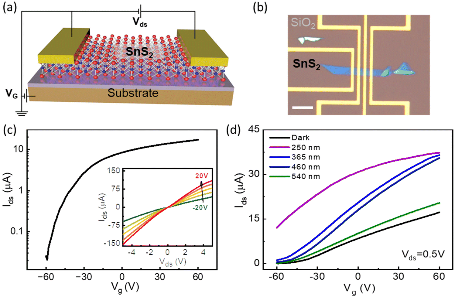 | ||
| Fig. 1 Device architecture and electrical response of the SnS2 FET. (a) Schematic diagram of the SnS2 device. (b) Optical image of the back-gated SnS2 device (L = 2 μm, W = 4.5 μm, and thickness = 13 nm) on a Si/SiO2 substrate. Scale bar: 10 μm. (c) Current vs. back gate voltage (Ids−Vg) plots in logarithmic scale at Vds = 0.5 V. The inset shows the current vs. source-to-drain voltage (Ids−Vds) plots at Vg values ranging from −20 to 20V with the step of 10V. (d) Ids−Vg trajectories of pristine SnS2 under different light illuminations. | ||
We performed the basic electrical measurements (transfer and output curves) on the multilayer SnS2 FET in the dark, which is followed by an optoelectronic response under continuous wave lasers of different wavelengths. Note that all the measurements were performed under ambient conditions throughout this study. Fig. 1c shows the transfer curve obtained by sweeping the gate voltages (Vg) from −60 to +60 V at a constant bias voltage (Vds = 0.5 V) under dark. The Ids−Vg trend shows typical n-type (electron dominant) characteristics of the SnS2 device, indicating that the Fermi level is positioned in the vicinity of the conduction band of SnS2. Similar to MoS2, the electron-rich characteristics in SnS2 are attributed to the presence of sulfur vacancies and the strong Fermi level pinning effect close to the conduction band edge in SnS2.24,25 The device shows a current ON/OFF ratio of ∼103. From the slope of the transfer curve, i.e., transconductance (gm), we calculated an effective field-effect mobility (μFE) of ∼20 cm2 V−1 s−1 using eqn (1).26
 | (1) |
cm−2 for 300 nm thick SiO2). The low-resistive electrical contacts between Cr/Au and the SnS2 channel are confirmed by realizing the almost linear output characteristics at all the measured Vg values of −20 to 20 V with a step of 10 V, as shown in the inset of Fig. 1c. Furthermore, the optoelectronic response of SnS2 at given laser wavelengths at a fixed laser power (Pint = 10 mWcm−2) and Vds = 0.5 V is compiled in Fig. 1d. The SnS2 device exhibits robust photoactive performance under incident wavelengths with a large photocurrent at shorter wavelengths due to the large photon energy. Under larger wavelength (over 540 nm) excitation, the device exhibits a very weak photocurrent as the incident photon energy is smaller than the optical band gap of multilayer SnS2 (∼2.3 eV). This limits the applicability of large bandgap materials for broadband photodetection. To address this issue, we employed a subtle technique by decorating metallic nanoparticles over SnS2 flakes. Silver, being relatively inexpensive compared to gold, has a higher refractive index at shorter wavelengths. Similarly, silver nanoparticles, Ag-NPs, exhibit plasmonic resonances at relatively shorter wavelengths.27
2.2 Ag-NPs-decorated SnS2 FETs
We, therefore, decorated Ag-NPs with a density of 40–45 NPs μm−2 over a fresh SnS2 phototransistor, as shown in the field emission scanning electron microscopy image in the inset of Fig. 2a. Note that the following results are obtained from different devices compared to Fig. 1; therefore, the maximum current levels are different in Fig. 2a as compared to Fig. 1c due to the device-to-device variation. From the comparative plots in Fig. 2a, we realized an almost two times increase in the on-state current from 1.39 μA to 2.75 μA after Ag-NPs deposition over SnS2. As a result, the SnS2 device shows a two-times increase in μFE from ∼15 to ∼32 cm2 V−1s−1, a shift in the threshold voltage (ΔVth ≈ 5 V) from −23 to −28 V and an increase in the electron density concentration [ne = Cox(Vg − Vth)] from ∼3 × 10¹² to ∼5.5 × 1012 cm−2, as shown in Fig. 2b and ESI S3.† These changes confirm the electron doping of SnS2 with Ag-NPs deposition induced by the surface charge transfer doping from Ag-NPs to SnS2 flakes.
 | ||
| Fig. 2 Optoelectronic performance before and after Ag-NPs deposition. (a) Comparative transfer curves of the SnS2 device (L = 2.2 μm, W = 4.1 μm, and thickness = 4.8 nm) before and after Ag-NPs deposition. (b) Comparison of the extracted field effect mobility and threshold voltage from (a). (c) Photocurrents of pristine SnS2 and Ag-NPs-decorated SnS2 devices at Vds = 0.5 V and Vg = 0. The light intensity was kept at 10 mW cm−2 during all the incident wavelengths. (d) Rise (green shaded) and decay (brown shaded) times of SnS2 and SnS2/Ag-NPs photodetectors obtained from temporal photocurrent measurements. (e) The generated photocurrent of SnS2 and SnS2/Ag-NPs devices as a function of illumination power density at Vg = 0V, where the dashed lines represent power-law fitting. | ||
We next focus on optoelectrical characteristics of pristine and Ag-NPs-decorated SnS2 phototransistors that were investigated at different wavelengths. The pristine SnS2 device demonstrated the photoresponse across a narrow spectral range (250–540 nm). Interestingly, the photocurrent of the same device increases by two times after depositing Ag-NPs, and the cut-off wavelength is extended to 1050 nm, as shown in Fig. 2c, which is attributed to the enhanced absorption and the photoluminescence effect in 2D materials by Ag-NPs.28,29 The extension in the detection range of the SnS2 device to near IR is mainly caused by the enhanced and broadband optical absorption in the NPs-decorated SnS2 devices.30 We think that this enhancement is the combined effect of several factors.31–33 First is the localized surface plasmon resonance (LSPR); the free electrons in Ag-NPs collectively oscillate at specific frequencies under illumination, leading to enhanced optical absorption and scattering by the NPs, and eventual enhancement in the photocurrent generation in SnS2. The resonance frequencies depend on the size, shape, and wavelength of incident light, and can be studied in detail by employing finite element analysis in future. Second is light trapping; the Ag-NPs over the SnS2 surface scatter the incident light, which is collected by neighboring NPs as plasmons instead of dissipating as free-space light, thus the strong optically interacting NPs trap light and increase the effective optical length and enhance the optical absorption, and hence an enhanced optoelectronic response in NPs-coacted SnS2 device is observed. Third is the generation of hot electrons; the extinction of plasmons in the Ag-NPs may generate energetic, non-equilibrium charged carriers, also called hot electrons, which can be transferred to the SnS2 surface, thus improving the photoresponsivity over a broad spectral range. We further compared the photodetector performances by estimating the rise and decay times of photodetectors from time-dependent photocurrent measurements. We obtained the rise and decay time responses by fitting the temporal photocurrent dataset, as shown in ESI Fig. S4,† by using eqn (2)
 | (2) |
2.3 Passivated SnS2/Ag-NPs/HfO2 photodetector
Compared to other noble metal-based NPs, Ag-NPs are reported to be oxidized under ambient conditions, and this effect can be exaggerated under illumination conditions.39 As a result, the performance of the Ag-NPs-coated SnS2 device may degrade over time. To circumvent this, we deposited a ∼15 nm thick high-k dielectric, HfO2, by atomic layer deposition, as indicated in Fig. 3a schematic. The stabilities and performances of the pristine SnS2, SnS2/NPs, and SnS2/Ag-NPs/HfO2 devices were monitored under ambient conditions for the first seven weeks (Fig. 3b). For more details, see ESI S5 and S6.† Among these three different device configurations, SnS2/Ag-NPs/HfO2 demonstrated the highest photoresponsivity (Rph = Iph/Pop × A; where Pop is the illuminated laser power and A is the active device area) of ∼12500 A W−1 at λ = 250 nm. Moreover, from the aging test result, we realized that the Rph is reduced by ∼20%, ∼36%, and 6% for the SnS2, SnS2/Ag-NPs, and SnS2/Ag-NPs/HfO2 photodetectors after seven weeks under similar storage and operation conditions, as shown in Fig. 3c. This phenomenon is ascribed to the direct impact of oxygen on bare SnS2, leading to the deterioration of material quality. In the case of SnS2/Ag-NPs, the degradation is more pronounced due to surface oxidation and the consequent depreciation of the interface between SnS2 and Ag-NPs. However, the introduction of HfO2 passivation emerges as a pivotal mitigating factor. This passivation layer effectively impedes the interaction of oxygen with SnS2 and Ag-NPs, thereby resulting in a mere 6% degradation and ensuring the stability of the devices with consistent performance. In a nutshell, the passivated SnS2/Ag-NPs/HfO2 photodetectors exhibit more stable performance for several weeks.
 | ||
| Fig. 3 Optoelectronic measurements of the HfO2-passivated SnS2/Ag-NPs device. (a) Schematic illustration of the HfO2-passivated SnS2/Ag-NPs device. (b) and (c) Comparison of the photoresponsibilities of SnS2, SnS2/Ag-NPs, and passivated SnS2/Ag-NPs/HfO2 photodetectors in first seven weeks in an ambient environment. (d) Comparison of the external quantum efficiencies of SnS2, SnS2/Ag-NPs, and passivated SnS2/Ag-NPs/HfO2 photodetectors at the given wavelengths of light. | ||
For further comparison among the three device configurations, we computed the external quantum efficiency (EQE = hcRph/eλ; where h is the Planck constant, c is the speed of light, and e is the elementary charge), which demonstrates the total electron–hole pair generation with the energy of one photon. The EQE was estimated to be ∼8.7 × 10⁵, ∼2.4 × 10⁶, and ∼5.9 × 10⁶% for SnS2, SnS2/NPs, and SnS2/NPs/HfO2, respectively. It is pertinent to note that our SnS2/NPs/HfO2 device exhibited superior EQE value compared to previous reports, which are summarized in Table 1.
| Material | Responsivity (A W−1) | Detectivity (Jones) | EQE (%) | Response time (rising, decay) sec | Ref. |
|---|---|---|---|---|---|
| SnS2 | 300 | 6 × 10⁹ | 4.6 × 10⁴ | 36, 7 | 40 |
| SnS2 | 8.8 × 10⁻³ | 109 | 24 | 0.005, 0.007 | 41 |
| SnS2 | 100 | — | 3.3 × 10⁴ | 330, 130 | 42 |
| SnS2 | 2 | — | 42, 42 | 43 | |
| SnS2 | 260 | 1.9 × 10¹⁰ | 9.3 × 10⁴ | 20, 16 | 44 |
| SnS2 | 1.19 | 1, 1 | 45 | ||
| SnS2 | 354 | 2 × 10¹⁰ | 1.1 × 10⁵ | 0.4, 0.5 | 46 |
| MoS2 Ag-NPs decorated | 2.9 × 10⁴ | 18, 7 | 47 | ||
| SnS2 Ag-NPs decorated | 1.2 × 10⁴ | — | 5.9 × 10⁶ | 7, 16 | This work |
2.4 Mechanical flexibility of the SnS2/Ag-NPs photodetector
Among other advantages, 2D materials are mechanically robust, thus they can be incorporated for flexible applications. Therefore, we investigated the mechanical endurance of the Ag-NPs-coated SnS2 photodetectors by bending polyethylene naphthalate (PEN) substrates with different radii, as shown schematically in Fig. 4a. The photoresponses as a function of time characteristics of the SnS2/Ag-NPs photodetectors were investigated at λ = 250 nm while holding the device at the bending position of various radii (0–flat, 20 mm, and 10 mm). Furthermore, we also illuminated at different light wavelengths (λ = 250, 540, and 1050 nm) at three different bending curvatures. | ||
| Fig. 4 Optoelectronic measurements of flexible SnS2/Ag-NPs devices. (a) Schematic drawing of the flexible photodetector of SnS2/Ag-NPs. (b) Temporal photoresponse of the flexible SnS2/Ag-NP photodetector under the given bending curvatures at λ = 250 nm and P = 10 mW cm−2. (c) Photoresponsivity of the flexible SnS2/Ag-NPs photodetector at different wavelengths (λ = 250, 540, and 1050 nm). (d) Time-dependent photoresponse in different numbers of bending cycles. (e) Reduction of photoresponsivity of the SnS2/Ag-NPs photodetector after various bending cycles. The bent radius was kept at 20 mm. The inset shows the flexible device in a bent position under light illumination. | ||
Fig. 4c depicts that the photoresponsivity of the flexible photodetector at 0 (flat), 20, and 10 mm was found to be ∼4778, ∼4575, and ∼4332 A W−1 at λ = 250 nm, respectively. The results show that the photoresponse remains persistent at different curvature states, thereby indicating that the devices exhibit excellent mechanical flexibility and broadband photodetection which are hardly affected by bending conditions. Moreover, the bending stability and reliability are the key factors of flexible photodetectors. Therefore, we bent (20 mm) our devices several times and measured the endurance of the photocurrent. From Fig. 4d, it is observed that the photoresponsivity of the flexible photodetector is ∼4556, ∼4523, ∼4101, and ∼3561 after bending for 0, 50, 100, and 150 cycles, respectively. Importantly, after 150 cycles, the photoresponsivity of the device decreased by ∼21%, which endorsed the photodetection stability of the flexible SnS2/Ag-NPs device under multiple bending cycles of 20 mm curvature. Furthermore, to observe the mechanical stability we calculated the response time of flexible the SnS2/Ag-NPs device at λ = 250 nm at various bending states. It is found that the response times are slightly reduced from 5.3 to 4.5 s (rise) and 6.7 to 6.1 s (decay) as the bending curvature is increased as shown in Fig. S8.† The reduction of response may be attributed to the defect states produced by stretching of the channel material SnS2. However, the flexible measurements clearly exhibit repeated bending, making it an attractive material for wearable photodetectors.
3. Conclusion
In summary, we have reported multilayer SnS2, SnS2/Ag-NP, and SnS2/Ag-NPs/HfO2 transistors to elucidate the light–matter interaction for broadband photodetectors. The light sensing capabilities of SnS2 are extended from the UV to near NIR (250–1050 nm) spectrum after decorating with Ag-NPs, which endorsed the extension of the cut-off wavelength in SnS2. These results suggest the enhanced light absorption with localization of the electromagnetic field via the surface plasmon-enhanced optical field and the wide band gap of SnS2 crystals. Furthermore, the photodetection performance, such as the photocurrent, photoresponsivity, and EQE, is significantly enhanced in the passivated Ag-NP-decorated SnS2 devices when compared to the bare SnS2 devices. In addition, we estimated the photo-performance deterioration of each device, where it was found that the SnS2/Ag-NPs/HfO2 device showed excellent stability with a meager reduction in photoresponsivity as compared to other devices. Moreover, we made a flexible SnS2/Ag-NPs photodetector, which showed a broadband light response having stability up to 500 bending cycles at a 20 mm curvature. Thus, our results provide an efficient approach to extend the optical and flexible sensing capabilities in wide bandgap 2D materials from UV to NIR for multifunctional photoelectronic devices.4. Materials and methods
To make large-scale patterns on Si/SiO2 substrates, we first performed photolithography. The chips were sonicated in acetone and isopropanol solvents, and later rinsed with piranha solution and washed with de-ionized water for 15 minutes to ensure the proper removal of contamination from the Si/SiO2 chips. The chips were soft-baked in a furnace at 125 °C to remove moisture. The 2D crystals of SnS2 were physically peeled off from the bulk crystals using a scotch tape and transferred to pre-patterned Au contact pads on Si/SiO2 wafers by the dry transfer method using the polydimethylsiloxane (PDMS) stamp technique. We used atomic force microscopy (AFM), XE-100 by Park Systems Inc., for precise thickness measurements of the SnS2 flakes. Subsequently, we performed electron beam lithography (EBL) to pattern metal electrodes. After EBL, we evaporated the Cr and Au metals of 5 and 80 nm thick, respectively, for metallization of the electrodes. Finally, the devices were immersed in acetone to lift-off the excess metal from the substrate. In addition, for flexible measurements, we used polyethylene naphthalate (PEN) substrates to fabricate the SnS2/Ag-NPs photodetector. Raman spectroscopy (Renishaw, In Via systems) was performed with a laser source of 514 nm under ambient conditions. Furthermore, atomic layer deposition (ALD) was used to deposit HfO2 (∼15 nm) at 250 °C at a rate of 0.1 nm per cycle. Electrical measurements were performed by employing a voltmeter (Keithley 2400) and a picoammeter (Keithley 6485).Conflicts of interest
All authors have no conflict to declare.Acknowledgements
This work was supported by the National Research Foundation (NRF) of Korea basic research grant funded by the Korean Government (MSIT) (No. 2022R1F1A1065232 and 2021R1A4A1031900) and the Global Research and Development Center Program (No. 2018K1A4A3A01064272). The authors extend their appreciation to the Deputyship for Research and Innovation, "Ministry of Education" in Saudi Arabia for funding this research (IFKSUOR3-39-1). This work was also supported by the Academy of Finland [Grant No. 320167 (PREIN Flagship – Aalto University)]. This work was supported by the National Research Foundation of Korea (NRF) basic research grant funded by the Korean government (MSIT) (No. 2022R1F1A1075229).References
- O. Lopez-Sanchez, D. Lembke, M. Kayci, A. Radenovic and A. Kis, Ultrasensitive Photodetectors Based on Monolayer MoS2, Nat. Nanotechnol., 2013, 8(7), 497–501 CrossRef CAS PubMed.
- X. Wang, D. Pan, M. Sun, F. Lyu, J. Zhao and Q. Chen, High-Performance Room-Temperature UV-IR Photodetector Based on the InAs Nanosheet and Its Wavelength- and Intensity-Dependent Negative Photoconductivity, ACS Appl. Mater. Interfaces, 2021, 13(22), 26187–26195 CrossRef CAS PubMed.
- Y. Chen, W. Ma, C. Tan, M. Luo, W. Zhou, N. Yao, H. Wang, L. Zhang, T. Xu, T. Tong, Y. Zhou, Y. Xu, C. Yu, C. Shan, H. Peng, F. Yue, P. Wang, Z. Huang and W. Hu, Broadband Bi2O2Se Photodetectors from Infrared to Terahertz, Adv. Funct. Mater., 2021, 31(14), 2009554 CrossRef CAS.
- O. Ozturk, B. M. Candan, S. Kurnaz, O. Cicek and A. T. Tasci, Solar Light Performances of N-ZnO Nanorods/p-Si-Based Photodetectors under High Illumination Intensity, J. Mater. Sci.: Mater. Electron., 2022, 33(18), 15222–15231 CrossRef CAS.
- A. Castellanos-Gomez, V. Singh, H. S. J. van der Zant and G. A. Steele, Mechanics of Freely-Suspended Ultrathin Layered Materials, Ann. Phys., 2015, 527(1–2), 27–44 CrossRef CAS.
- H. Chen, H. Liu, Z. Zhang, K. Hu and X. Fang, Nanostructured Photodetectors: From Ultraviolet to Terahertz, Adv. Mater., 2016, 28(3), 403–433 CrossRef CAS PubMed.
- S. Kaushik and R. Singh, 2D Layered Materials for Ultraviolet Photodetection: A Review, Adv. Opt. Mater., 2021, 9(11), 2002214 CrossRef CAS.
- Z. Wang, Q. Tu, S. Zheng, J. J. Urban, S. Li and B. Mi, Understanding the Aqueous Stability and Filtration Capability of MoS2 Membranes, Nano Lett., 2017, 17(12), 7289–7298 CrossRef CAS PubMed.
- M. P. Ulmer, Future UV Detectors for Space Applications, Proc. SPIE, Optical Sensing II, 2006, 6189, 1–10 Search PubMed.
- M. Kaliszewski, M. Włodarski, A. Bombalska, M. Kwaśny, M. Mularczyk-Oliwa, J. Młyńczak and K. Kopczyński, The Application of Semiconductor Based UV Sources for the Detection and Classification of Biological Material, Proc. SPIE, Laser Tech 2012: Applications for Laser, 2013, 8703, 24–31 Search PubMed.
- J. Kaur, M. Singh, C. Dell‘Aversana, R. Benedetti, P. Giardina, M. Rossi, M. Valadan, A. Vergara, A. Cutarelli, A. M. I. Montone, L. Altucci, F. Corrado, A. Nebbioso and C. Altucci, Biological Interactions of Biocompatible and Water-Dispersed MoS2 Nanosheets with Bacteria and Human Cells, Sci. Rep., 2018, 8(1), 16386 CrossRef PubMed.
- L. Huang, A. Krasnok, A. Alú, Y. Yu, D. Neshev and A. E. Miroshnichenko, Enhanced Light–Matter Interaction in Two-Dimensional Transition Metal Dichalcogenides, Rep. Prog. Phys., 2022, 85(4), 046401 CrossRef PubMed.
- A. Castellanos-Gomez, Black Phosphorus: Narrow Gap, Wide Applications, J. Phys. Chem. Lett., 2015, 6(21), 4280–4291 CrossRef CAS PubMed.
- E. V. Rusu, N. N. Syrbu, A. V. Tiron and V. V. Zalamai, Band Structure and Optical Constants of SnS2 Single Crystals, Mater. Res. Express, 2019, 6(4), 046203 CrossRef.
- L. Du, T. Hasan, A. Castellanos-Gomez, G.-B. Liu, Y. Yao, C. N. Lau and Z. Sun, Engineering Symmetry Breaking in 2D Layered Materials, Nat. Rev. Phys., 2021, 3, 193–206 CrossRef CAS.
- L. Britnell, R. M. Ribeiro, A. Eckmann, R. Jalil, B. D. Belle, A. Mishchenko, Y. J. Kim, R. V. Gorbachev, T. Georgiou, S. V. Morozov, A. N. Grigorenko, A. K. Geim, C. Casiraghi, A. H. C. Neto and K. S. Novoselov, Strong Light-Matter Interactions in Heterostructures of Atomically Thin Films, Science, 2013, 340(6138), 1311–1314 CrossRef CAS PubMed.
- C. Hsu, R. Frisenda, R. Schmidt, A. Arora, S. M. Vasconcellos, R. Bratschitsch, H. S. J. Zant and A. Castellanos-Gomez, Thickness–Dependent Refractive Index of 1L, 2L, and 3L MoS2, MoSe2, WS2, and WSe2, Adv. Opt. Mater., 2019, 7(13), 1900239 CrossRef.
- X. Jia, C. Tang, R. Pan, Y. Long, C. Gu and J. Li, Thickness-Dependently Enhanced Photodetection Performance of Vertically Grown SnS2 Nanoflakes with Large Size and High Production, ACS Appl. Mater. Interfaces, 2018, 10(21), 18073–18081 CrossRef CAS PubMed.
- M. F. Khan, S. Rehman, I. Akhtar, S. Aftab, H. M. S. Ajmal, W. Khan, D. Kim and J. Eom, High Mobility ReSe2 Field Effect Transistors: Schottky-Barrier-Height-Dependent Photoresponsivity and Broadband Light Detection with Co Decoration, 2D Mater., 2019, 7(1), 015010 CrossRef.
- S. Latini, E. Ronca, U. De Giovannini, H. Hübener and A. Rubio, Cavity Control of Excitons in Two-Dimensional Materials, Nano Lett., 2019, 19(6), 3473–3479 CrossRef CAS PubMed.
- S. Parhizkar, M. Prechtl, A. L. Giesecke, S. Suckow, S. Wahl, S. Lukas, O. Hartwig, N. Negm, A. Quellmalz, K. Gylfason, D. Schall, M. Wuttig, G. S. Duesberg and M. C. Lemme, Two-Dimensional Platinum Diselenide Waveguide-Integrated Infrared Photodetectors, ACS Photonics, 2022, 9(3), 859–867 CrossRef CAS PubMed.
- Y. Ding, W. Zheng, X. Lu, Y. Liang, Y. Zhu, M. Jin and F. Huang, Raman Tensor of Layered SnS2, J. Phys. Chem. Lett., 2020, 11(23), 10094–10099 CrossRef CAS PubMed.
- T. Sriv, K. Kim and H. Cheong, Low-Frequency Raman Spectroscopy of Few-Layer 2H-SnS2, Sci. Rep., 2018, 8(1), 10194 CrossRef PubMed.
- P. Bampoulis, R. van Bremen, Q. Yao, B. Poelsema, H. J. W. Zandvliet and K. Sotthewes, Defect Dominated Charge Transport and Fermi Level Pinning in MoS2/Metal Contacts, ACS Appl. Mater. Interfaces, 2017, 9(22), 19278–19286 CrossRef CAS PubMed.
- D. Liu, Y. Guo, L. Fang and J. Robertson, Sulfur Vacancies in Monolayer MoS2 and Its Electrical Contacts, Appl. Phys. Lett., 2013, 103(18), 183113 CrossRef.
- M. F. Khan, F. Ahmed, S. Rehman, I. Akhtar, M. A. Rehman, P. A. Shinde, K. Khan, D. Kim, J. Eom, H. Lipsanen and Z. Sun, High Performance Complementary WS2 Devices with Hybrid Gr/Ni Contacts, Nanoscale, 2020, 12(41), 21280–21290 RSC.
- S. Malynych and G. Chumanov, Light-Induced Coherent Interactions between Silver Nanoparticles in Two-Dimensional Arrays, J. Am. Chem. Soc., 2003, 125(10), 2896–2898 CrossRef CAS PubMed.
- B. Sun, Z. Wang, Z. Liu, X. Tan, X. Liu, T. Shi, J. Zhou and G. Liao, Tailoring of Silver Nanocubes with Optimized Localized Surface Plasmon in a Gap Mode for a Flexible MoS2 Photodetector, Adv. Funct. Mater., 2019, 29(26), 1900541 CrossRef.
- D. Mouloua, M. El Marssi, M. A. El Khakani and M. Jouiad, Enhanced photodetection properties of CVD-grown MoS2 nanosheets onto Ag-nanoparticles decorated substrates, in IEEE EUROCON 2023–20th International Conference on Smart Technologies, IEEE, Torino, Italy, 2023, pp. 138–141. DOI:10.1109/EUROCON56442.2023.10199014.
- R. Liu, F. Wang, L. Liu, X. He, J. Chen, Y. Li and T. Zhai, Band Alignment Engineering in Two-Dimensional Transition Metal Dichalcogenide-Based Heterostructures for Photodetectors, Small Struct., 2021, 2(3), 2000136 CrossRef CAS.
- L. Chang, L. V. Besteiro, J. Sun, E. Y. Santiago, S. K. Gray, Z. Wang and A. O. Govorov, Electronic Structure of the Plasmons in Metal Nanocrystals: Fundamental Limitations for the Energy Efficiency of Hot Electron Generation, ACS Energy Lett., 2019, 4(10), 2552–2568 CrossRef CAS.
- Y. Li, W. Shi, A. Gupta and N. Chopra, Morphological Evolution of Gold Nanoparticles on Silicon Nanowires and Their Plasmonics, RSC Adv., 2015, 5(61), 49708–49718 RSC.
- C. V. Hoang, K. Hayashi, Y. Ito, N. Gorai, G. Allison, X. Shi, Q. Sun, Z. Cheng, K. Ueno, K. Goda and H. Misawa, Interplay of Hot Electrons from Localized and Propagating Plasmons, Nat. Commun., 2017, 8(1), 771 CrossRef PubMed.
- W. Jing, N. Ding, L. Li, F. Jiang, X. Xiong, N. Liu, T. Zhai and Y. Gao, Ag Nanoparticles Modified Large Area Monolayer MoS2 Phototransistors with High Responsivity, Opt. Express, 2017, 25(13), 14565–14574 CrossRef CAS PubMed.
- J. Pak, I. Lee, K. Cho, J. K. Kim, H. Jeong, W. T. Hwang, G. H. Ahn, K. Kang, W. J. Yu, A. Javey, S. Chung and T. Lee, Intrinsic Optoelectronic Characteristics of MoS2 Phototransistors via a Fully Transparent van der Waals Heterostructure, ACS Nano, 2019, 13(8), 9638–9646 CrossRef CAS PubMed.
- H. Fang and W. Hu, Photogating in Low Dimensional Photodetectors, Adv. Sci., 2017, 4(12), 1700323 CrossRef PubMed.
- Y. Wang, X. Huang, D. Wu, R. Zhuo, E. Wu, C. Jia, Z. Shi, T. Xu, Y. Tian and X. Li, A Room-Temperature near-Infrared Photodetector Based on a MoS2/CdTe p–n Heterojunction with a Broadband Response up to 1700 nm, J. Mater. Chem. C, 2018, 6(18), 4861–4865 RSC.
- G. Wu, X. Wang, Y. Chen, Z. Wang, H. Shen, T. Lin, W. Hu, J. Wang, S. Zhang, X. Meng and J. Chu, Ultrahigh Photoresponsivity MoS2 Photodetector with Tunable Photocurrent Generation Mechanism, Nanotechnology, 2018, 29(48), 485204 CrossRef PubMed.
- N. Grillet, D. Manchon, E. Cottancin, F. Bertorelle, C. Bonnet, M. Broyer, J. Lermé and M. Pellarin, Photo-Oxidation of Individual Silver Nanoparticles: A Real-Time Tracking of Optical and Morphological Changes, J. Phys. Chem. C, 2013, 117(5), 2274–2282 CrossRef CAS.
- X. Zhou, L. Gan, Q. Zhang, X. Xiong, H. Li, Z. Zhong, J. Han and T. Zhai, High Performance Near-Infrared Photodetectors Based on Ultrathin SnS Nanobelts Grown via Physical Vapor Deposition, J. Mater. Chem. C, 2016, 4(11), 2111–2116 RSC.
- G. Su, V. G. Hadjiev, P. E. Loya, J. Zhang, S. Lei, S. Maharjan, P. Dong, P. M. Ajayan, J. Lou and H. Peng, Chemical Vapor Deposition of Thin Crystals of Layered Semiconductor SnS2 for Fast Photodetection Application, Nano Lett., 2015, 15(1), 506–513 CrossRef CAS PubMed.
- Y. Huang, H. Deng, K. Xu, Z. Wang, Q. Wang, F. Wang, F. Wang, X. Zhan, S. Li, J. Luo and J. He, Highly sensitive and fast phototransistor based on large size CVD-grown SnS2 nanosheets, Nanoscale, 2015, 7, 14093–14099 RSC.
- J. Xia, D. Zhu, L. Wang, B. Huang, X. Huang and X.-M. Meng, Large-Scale Growth of Two-Dimensional SnS2 Crystals Driven by Screw Dislocations and Application to Photodetectors, Adv. Funct. Mater., 2015, 25(27), 4255–4261 CrossRef CAS.
- X. Zhou, Q. Zhang, L. Gan, H. Li and T. Zhai, Large–Size Growth of Ultrathin SnS2 Nanosheets and High Performance for Phototransistors, Adv. Funct. Mater., 2016, 26, 4405–4413 CrossRef CAS.
- D. Yang, B. Li, C. Hu, H. Deng, D. Dong, X. Yang, K. Qiao, S. Yuan and H. Song, Controllable Growth Orientation of SnS2 Flakes for Low-Noise, High-Photoswitching Ratio, and Ultrafast Phototransistors, Adv. Opt. Mater., 2016, 4(3), 419–426 CrossRef CAS.
- X. Jia, C. Tang, R. Pan, Y. Long, C. Gu and J. Li, Thickness-Dependently Enhanced Photodetection Performance of Vertically Grown SnS2 Nanoflakes with Large Size and High Production, ACS Appl. Mater. Interfaces, 2018, 10(21), 18073–18081 CrossRef CAS PubMed.
- W. Jing, N. Ding, L. Li, F. Jiang, X. Xiong, N. Liu, T. Zhai and Y. Gao, Ag Nanoparticles Modified Large Area Monolayer MoS2 Phototransistors with High Responsivity, Opt. Express, 2017, 25(13), 14565–14574 CrossRef CAS PubMed.
Footnotes |
| † Electronic supplementary information (ESI) available. See DOI: https://doi.org/10.1039/d3nr04626e |
| ‡ These authors contributed equally to this work. |
| This journal is © The Royal Society of Chemistry 2024 |