
Contemporary innovations in two-dimensional transition metal dichalcogenide-based P–N junctions for optoelectronics
Ehsan
Elahi
 *a,
Muneeb
Ahmad
b,
A.
Dahshan
c,
Muhammad
Rabeel
b,
Sidra
Saleem
d,
Van Huy
Nguyen
e,
H. H.
Hegazy
cf and
Sikandar
Aftab
*g
*a,
Muneeb
Ahmad
b,
A.
Dahshan
c,
Muhammad
Rabeel
b,
Sidra
Saleem
d,
Van Huy
Nguyen
e,
H. H.
Hegazy
cf and
Sikandar
Aftab
*g
aDepartment of Physics & Astronomy and Graphene Research Institute, Sejong University, 209 Neungdong-ro, Gwangjin-Gu, Seoul 05006, South Korea. E-mail: Ehsanelahi@sju.ac.kr
bDepartment of Electrical Engineering and Convergence Engineering for Intelligent Drone, Sejong University, 209 Neungdong-ro, Gwangjin-Gu, Seoul 05006, South Korea
cDepartment of Physics, Faculty of Science, King Khalid University, P.O. Box 9004, Abha, Saudi Arabia
dDivision of Science Education, Department of Energy Storage/Conversion Engineering for Graduate School, Jeonbuk National University, Jeonju, Jeonbuk 54896, Republic of Korea
eDepartment of Nanotechnology and Advanced Materials Engineering, and H.M.C., Sejong University, Seoul 05006, South Korea
fResearch Centre for Advanced Materials Science (RCAMS), King Khalid University, P. O. Box 9004, Abha 61413, Saudi Arabia
gDepartment of Intelligent Mechatronics Engineering, Sejong University, 209 Neungdong-ro, Gwangjin-Gu, Seoul, 05006 South Korea. E-mail: aftab@sejong.ac.kr
First published on 29th November 2023
Abstract
Two-dimensional transition metal dichalcogenides (2D-TMDCs) with various physical characteristics have attracted significant interest from the scientific and industrial worlds in the years following Moore's law. The p–n junction is one of the earliest electrical components to be utilized in electronics and optoelectronics, and modern research on 2D materials has renewed interest in it. In this regard, device preparation and application have evolved substantially in this decade. 2D TMDCs provide unprecedented flexibility in the construction of innovative p–n junction device designs, which is not achievable with traditional bulk semiconductors. It has been investigated using 2D TMDCs for various junctions, including homojunctions, heterojunctions, P–I–N junctions, and broken gap junctions. To achieve high-performance p–n junctions, several issues still need to be resolved, such as developing 2D TMDCs of superior quality, raising the rectification ratio and quantum efficiency, and successfully separating the photogenerated electron–hole pairs, among other things. This review comprehensively details the various 2D-based p–n junction geometries investigated with an emphasis on 2D junctions. We investigated the 2D p–n junctions utilized in current rectifiers and photodetectors. To make a comparison of various devices easier, important optoelectronic and electronic features are presented. We thoroughly assessed the review's prospects and challenges for this emerging field of study. This study will serve as a roadmap for more real-world photodetection technology applications.
 Ehsan Elahi | Ehsan Elahi is a PhD student who is currently working in the Department of Physics (Sejong University). He obtained his M.Sc. in Electronics from Quaid-i-Azam University Islamabad Pakistan and his M.Phil. from Riphah International University Lahore Campus, Punjab, Pakistan. Ehsan's research interests include 2D materials (TMDCs), 2D Ferromagnetic materials, Electronics, Optoelectronics, Spintronics, and Spin-caloritronics. |
 Muneeb Ahmad | Mr Muneeb Ahmad is currently working as an MS-Ph.D. student in the Nano-device Laboratory, Department of Semiconductor Systems Engineering, Sejong University, South Korea. He obtained his BS in Materials Science and Engineering from the Institute of Space Technology, Islamabad, Pakistan. His main area of work is resistive memory devices, transistors, and solar cells. |
 Muhammad Rabeel | Mr Muhammad Rabeel is a dedicated Ph.D. student at the Nano-device Laboratory in the Department of Electrical Engineering at Sejong University, South Korea. He obtained his master's degree from the School of Chemical & Materials Engineering (SCME) at the National University of Sciences and Technology (NUST) in Islamabad, Pakistan. His research interests primarily revolve around the fascinating world of 2D materials and their diverse applications. Specifically, he has a strong passion for exploring their potential in sensing applications, as well as their use in the development of flexible photodetectors, logic gates, and photocatalysis. |
 Sidra Saleem | Sidra Saleem is a Ph.D. student in the Department of Energy Storage and Conversion Engineering at Jeonbuk National University, Jeonju, South Korea. Her research primarily focused on water splitting, specifically addressing the Hydrogen Evolution Reaction (HER), Oxygen Evolution Reaction (OER), and Oxygen Reduction Reaction (ORR) for energy storage devices. |
 Van Huy Nguyen | Dr Van Huy Nguyen is a research associate at the University of Manchester, UK. He obtained his Ph.D. in Nanotechnology and Advanced Materials Engineering from Sejong University, South Korea, in 2023. His primary research interests are focused on 2D materials, including graphene and TMDCs, based on their heterostructures for energy harvesting and storage devices. |
 Sikandar Aftab | Sikandar Aftab earned his Ph.D. in Physics from the Department of Physics and Graphene Research Institute, Sejong University, South Korea. He also completed a two-year post-doctoral fellowship at Simon Fraser University in Burnaby, Canada. Dr Aftab is currently employed as an Assistant Professor at Sejong University's Department of Intelligent Mechatronics Engineering in Seoul, South Korea. His research interests include nanodevices based on two-dimensional materials heterostructures, energy storage devices and solar cells. |
1. Introduction
Two-dimensional (2D) layered materials are recognized as potential prospects in the fields of electronics and optoelectronics owing to their striking physical characteristics.1–6 2D materials have established a significant deal of devotion in the fields of spintronics,7–12 electronics,13–17 and optoelectronics.15,18–24 Scientists were sure that heat fluctuation made it difficult for nanoparticles to maintain stability, which ultimately caused a breakdown. The thermally stable graphene in this scenario has greatly surprised scientists, spurring the rapid growth of the 2D materials research field over the past few decades.25,26 Because graphene shows a lack of bandgap configuration, it should potentially be competent in reacting to all photons, giving it the benefit of wide band revealing from ultraviolet (UV) to infrared (IR) and to the terahertz range.27–29 Apart from its extensive band response qualities, pure monolayer graphene has high transparency, with a wide band absorption of 2.3%.30 With such high transmittance, graphene has the potential to be used as a transparent electrode, particularly in devices with large absorption areas, such as solar cells and capacitors.31,32 Additionally, by changing the electronic Fermi level, it is possible to alter the broadband absorption of graphene, which may then control the photon transition in graphene nanosheets.33,34 With the contact of incoming light, energy might be transferred among carriers, photons, and phonons in graphene via charge carrier transition (electrons and holes). Macroscopical mechanisms, such as plasmons,35,36 non-linear optical characteristics,37–39 and photon absorption,40,41 have been observed previously.Group IV (Si, Ge, and Sn) element-based 2D materials have recently been developed. The structure of silicene and germanene is comparable to that of graphene, with an in-plane honeycomb lattice and van der Waals (vdW's) bonds linking neighboring layers. Because of their compatibility with Si technology, they have the potential to be used in integrated circuits. Another type of 2D material, black phosphorus (BP),42,43 was initially produced over a century ago and has recently sparked considerable attention because of its direct band gap in bulk and single-layer ranging from 0.33 to more than 1 eV. Therefore, BP can be used in mid-infrared photodetectors:44 a monolayer of BP has been exfoliated using the scotch tape technique and has a thickness of 0.7–0.85 nm. Regarding the electric characteristics of BP, it has been determined that the electron and hole mobilities are greater than 1000 cm2 V−1 s−1 under ambient conditions with an extraordinary on/off ratio from the application viewpoint with its suitable band structure, which makes it appropriate for photodetection.45,46 In addition, MXenes,47–49 which include carbonitrides, transition-metal carbides, and nitrides, have been thoroughly researched for use in electrical and optoelectronic appliances.50,51 Owing to the intrinsic p-type layered semiconductor characteristics, ultralow thermal conductivity, and near-infrared narrow band gap, tin selenide (SnSe) nanosheets have gained considerable attention.52–56 When combined with additional benefits, such as chemical stability, earth abundance, cheap cost, and nontoxicity, SnSe has a lot of promise for use in upcoming electronic circuit applications. InSe-based devices have undergone a comprehensive investigation of the visible spectrum, but they have not yet been thoroughly investigated for near-infrared (NIR) applications.57,58 The absence of on-chip sources and the elevated cost of manufacturing place further restrictions on optoelectronic devices for detection and sensing applications in the mid-infrared region.59–61 Most InSe-based optoelectronic devices are transistor-based, necessitating strong electrical bias gating and bias voltage.58,62,63 In another class, depending on the layer thickness, 2D transition metal dichalcogenide (TMDC)15–17,20,24,64,65 materials have band gaps between 1 and 2 eV. A broad range of applications, including photodetectors,66,67 are possible owing to the band gap variation between multilayer and monolayer direct gaps68,69 and field-effect transistor (FET),16,65,70–73 as well as optical communication.74,75 The fundamental components of diodes, transistors, photodetectors, and solar cells, which make up advanced electronics and optoelectronic relevance,20,23 are junctions that contain homo- and hetero-types.24,76–78 Significant studies have focused on the p–n interface made of various 2D materials, creating a novel material manifesto for investigating novel physical features and innovative device applications.79–85 It has been proven that layered MoS2, a member of the TMDC family, is a prominent material with outstanding electrical and optical characteristics.2,86,87 Thus, an innovative material, which provides a way for optoelectronic applications, is offered by the construction of p–n junctions using SnSe and MoS2 nanosheet. It is known that SnSe/MoS2 vertical p–n junctions are grown using a two-step CVD process, resulting in enhanced optoelectronic capabilities in the devised devices.88 A p–n interface consisting of 2D materials89–94 is a type of junction formed by combining a region of p-type layered material with a region of n-type material. The resulting junction has interesting electrical properties, including the ability to allow current to flow in only one direction. This property makes p–n junctions useful in an extensive range of electronic devices, including diodes, transistors, and solar cells. In a homojunction, when a semiconductor junction has a p-region and an n-region formed of the same 2D material, the term “p–n junction” is used. In other words, the junction is made up of the same kind of 2D materials on both sides but with varying degrees of doping, as shown in Fig. 1(a).95–97 The movement of charge carriers (electrons and holes) through the junction is governed by the potential barrier that is created at the junction owing to the difference in doping levels. A heterojunction p–n is a form of interface in which the p-region and n-region are constructed of separate 2D materials, as shown in Fig. 1(b).93,98,99 The p- and n-regions of heterojunction p–n are generally made up of materials with differing bandgaps and lattice architectures. The energy difference between the valence band (VB: where electrons are forcefully bound) and the conduction band (CB: where electrons are free to flow) is defined as the bandgap. The difference in bandgaps between a heterojunction's p-region and n-region provides a potential energy barrier at the interface. There are various advantages to employing a heterojunction p–n over a homojunction p–n diode. For instance, the difference in bandgaps provides improved charge carrier flow management and can lower leakage currents. Second, it allows for the engineering of band alignment, which can aid in the efficient flow of electrons or holes across junctions. A PIN junction100 is a type of semiconductor junction that consists of three layers: a p-type substance, an intrinsic (I) layer, and an n-type material. The name “PIN” is derived from the arrangement of these layers, as shown in Fig. 1(c). Because the intrinsic layer is usually broader than the P and N layers, it might operate as a barrier for the majority of carriers (electrons in the n area and holes in the p region). This barrier prohibits electron and hole recombination, resulting in a depletion zone inside the intrinsic layer. PIN junctions provide various benefits over traditional p–n junctions. The larger intrinsic layer enhances the area available for charge carrier separation and decreases the likelihood of recombination. This feature makes the PIN junction ideal for high-frequency signal applications, such as photodetectors and high-speed diodes. It improves the reaction speed, sensitivity, and efficiency of the device. A “broken gap p–n junction” refers to a type of p–n junction where the bandgap of a 2D material changes abruptly across the junction interface, as shown in Fig. 1(d).94,101,102 The p–n junctions with broken gaps are commonly employed in devices such as tunnel diodes and quantum well lasers. The tunneling phenomenon occurs in tunnel diodes owing to the broken gap p–n junction, which allows charge carriers to travel across the junction even when their energy levels do not align. Quantum well lasers, however, use the p–n junction's shattered gap to generate quantum confinement and regulate the light output at certain wavelengths. Overall, the broken gap p–n junction is a specialized arrangement with distinct properties when compared to normal p–n junctions, enabling specialized applications in electrical and optoelectronic devices.
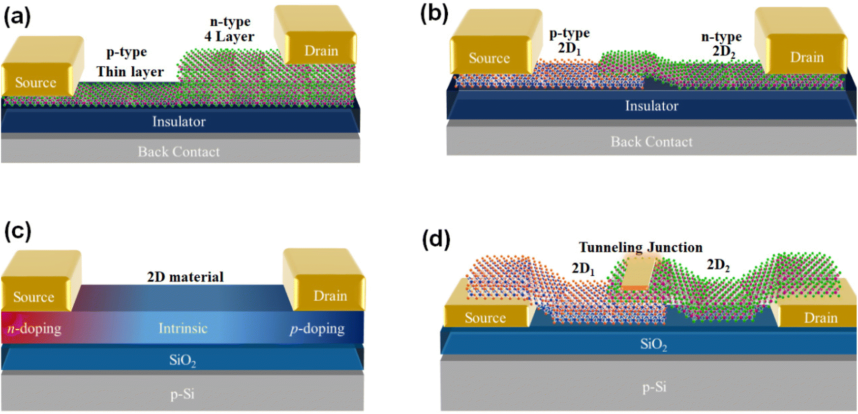 | ||
| Fig. 1 Various types of junctions. (a) Homojunction p–n. (b) Heterojunction p–n. (c) PIN junction. (d) Broken-gap p–n junction. | ||
This study considers current developments in reconfigurable electrical devices built on 2D materials. We explored 2D material-based p–n heterostructures and devices for photodetection. We explain the essentials of 2D materials, including their configuration, electrical and optoelectronic characteristics, and interactions with hybrid systems. Next, several topologies and associated nanodevices for photodetection, such as p–n junction diode, are described in depth. The device's performances were analyzed and summarized. This review, which is certainly of considerable interest to developers of p–n junction-based photodetectors, highlights the key features of 2D material heterostructure-based photodetectors.
2. Preparation techniques for heterojunctions
Several approaches for integrating 2D materials have been suggested to create a 2D heterostructure using TMDCs, including mechanical transfer and stacking procedures with exfoliated layers,103 chemical vapor deposition (CVD),83,104–106 Molecular Beam Epitaxy (MBE),107–110 and phase transition.1112.1. Mechanical exfoliation and restacking
One of the earliest methods of fabricating 2D materials is the exfoliation of monolayer graphene. With a thorough investigation of graphene and its related variants as well as other 2D materials with an analogous arrangement, such as the hexagonal boron nitride (h-BN),112 TMDCs,113 and “BP”,114 mechanically exfoliated and incredibly nano structural devices with remarkable performance were produced. The excellent optical and optoelectronic capabilities of these 2D materials have attracted increased attention in the study of optoelectronic devices.115 Owing to accessibility and versatility, mechanical exfoliation has developed into a simple method for producing 2D materials.116 Mechanical exfoliation is a straightforward technique for creating new layers of 2D materials (from one to many layers) while retaining crystal symmetry and other properties.117 The mechanical exfoliation process of the 2D materials is shown in Fig. 2(a). Adhesive tape is pressed into the bulk material, and the top layer becomes a segment of the tape. Once more, the tape is pushed with layers on the plane of the substrate. The bottom layer turns into part of the substrate when detached off. GaSe/SnS2 vertical heterojunction device with a clearly enhanced color contrast between the layer interface is shown in the optical microscope (OM) image form in Fig. 2(b). The devices were fabricated using the micromechanical cleavage technique. Fig. 2(c) shows that mechanical exfoliation was employed to create the high-quality multilayer WSe2 and α-In2Se3 flakes utilized in this study.118 Furthermore, PET has a comparatively extraordinary Young's modulus, ensuring that the produced strain during bending may be effectively transmitted to the 2D layers. Flakes of α-In2Se3 and WSe2 were exfoliated onto SiO2/Si substrates to begin the device's construction. Moreover, a PET substrate was used to produce Ti/Au (10 nm/50 nm) electrodes using conventional photolithography and e-beam evaporation. However, mechanically exfoliated WSe2–MoS2 p–n junction was investigated by Shin et al. The optical image of the fabricated device is demonstrated in Fig. 2(d).119 The WSe2–MoS2 p–n interface served as a charge transfer layer, while the MoS2 served as the phototransistor's channel. With a high photoresponsivity of 2700 A W−1, a specific detectivity of 5 × 10¹¹ Jones, and a reaction time of 17 ms, the suggested p–n device demonstrated exceptional performance. The p-GeSe/n-WS2 diode has remarkable optoelectronic and rectification properties as the optical image of the designed device (mechanically exfoliated), as illustrated in Fig. 2(e).120 The diode displayed effective photodetection with encouraging merit numbers. Investigation of the photoresponse is performed using illuminations of λ = 850, 530 and 365 nm. At 850 nm, the diode has a strong response of 845 mA W−1. The diode also has a detectivity of 3.28 × 10⁸ Jones. Remote sensing, target tracking, and computer vision are all possible uses of near-infrared polarization-sensitive photodetectors because of their benefits in efficiently recording light signals while blocking unwanted light. By stacking multilayer p-type GeSe atop n-type MoTe2 with a mechanical exfoliation approach, a self-powered photodetector that is 2D polarization sensitive is developed, as shown in Fig. 2(f).121 Broadband spectrum representation from the visible (405 nm) to near-IR (1310 nm) wavelength range is displayed by the device. The responsivity (R) and detectivity (D*) at zero bias and 808 nm light can be as high as 52 mA W−1 and 4.1 × 10¹¹ Jones, respectively. An efficient method for creating self-powered devices with incorporated angle-resolved optoelectronic devices is shown in this study by employing GeSe/MoTe2 heterojunctions.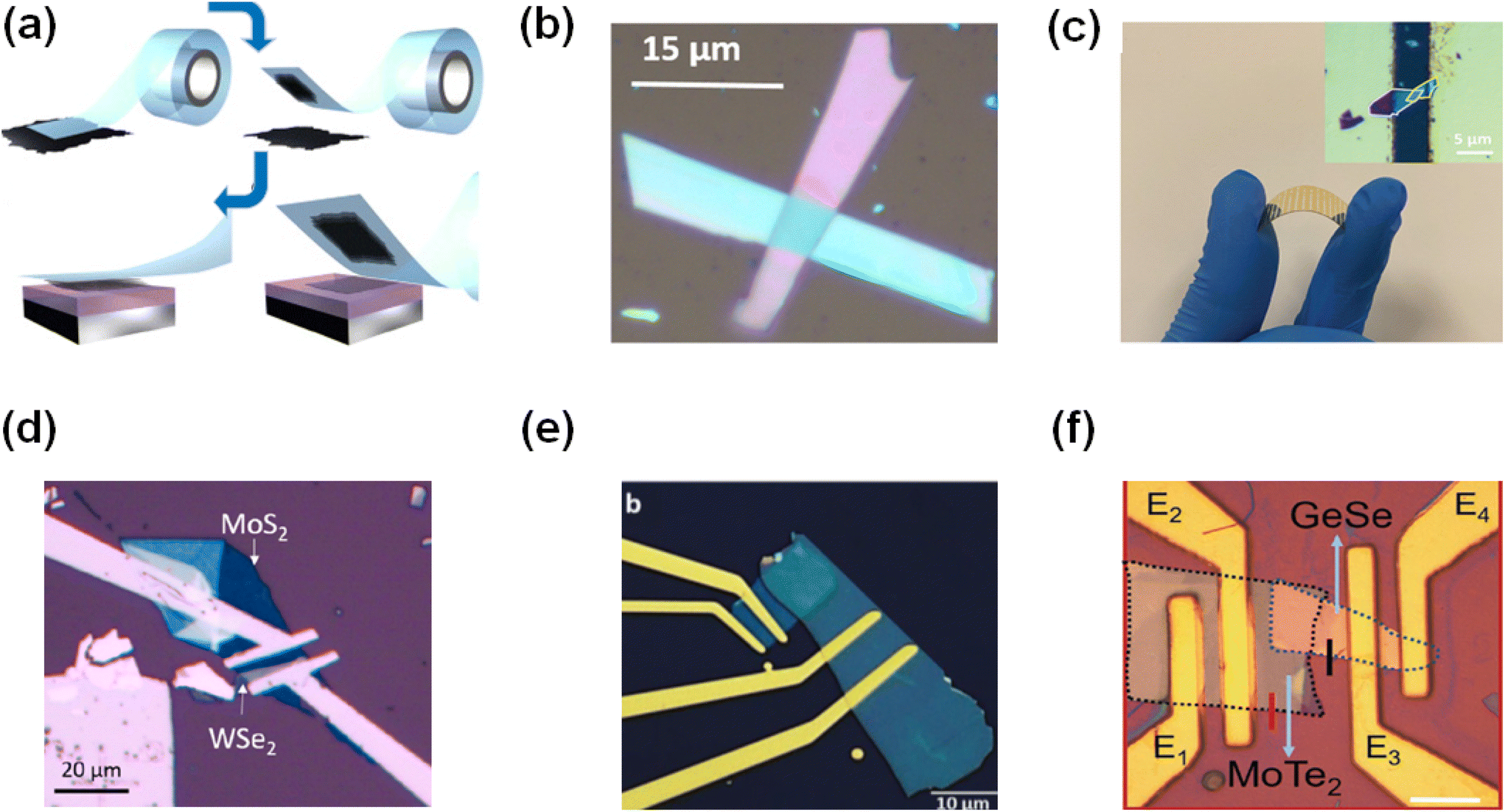 | ||
| Fig. 2 (a) Process of mechanical exfoliation.122 (b) Optical microscope image of a fabricated GaSe/SnS2 p–n heterostructure by exfoliation. This figure is reproduced from ref. 123, copyright, Appl. Surface Sci., 2021, 535, 147480. (c) Optical image of mechanically exfoliated α-In2Se3/WSe2 heterojunction under tensile strain. This figure is reproduced by ref. 118, copyright, Adv. Opt. Mater., 2021. (d) The device is based on WSe2−MoS2 vdW's heterostructure. This figure is replicated by ref. 119, copyright, Nano Lett., 2020, 20.8. (e) Optical picture of a Pd/Au and Cr/Au electrode p-GeSe/n-WS2 diode. This figure is reproduced by the authorization of ref. 120, copy right, Adv. Mater. Interfaces, 2020. (f) Image of a GeSe/MoTe2 p–n junction device taken using an optical microscope. This figure is replicated by ref. 121, copyright, Adv. Mater. Interfaces, 2022. | ||
2.2. Chemical vapor deposition (CVD)
Several 2D material-based FETs have been recognized as having potential for usage in multifunctional devices for optoelectronics, photonics and nanoelectronics at the nanoscale69,124 since scientists began studying graphene as a photodiode in 2009.18,125 TMDC materials, particularly monolayer MoSe2 and WSe2, have attracted a lot of interest as next-generation materials. Their semiconducting properties, direct bandgap, substantial absorption coefficient, and band-gap features are adjustable by changing the thickness of the material as well as electrically by the field effect, and they are ideal materials for ultrathin electronic and optoelectronic ICs.124,126 However, whether used in a device with greater sensitivity or with a broad absorption spectrum, single 2D TMDC materials have some limits.126,127 Thus, the hybridization of materials with various optical characteristics significantly simplifies optical engineering.128 Various methods have been employed for this purpose. The CVD approach, which is both cost effective and time efficient, is commonly employed for the fabrication of 2D heterostructures.83,105 Vertical structures associated with vdW forces or covalently bonded lateral heterostructures can be created via CVD. The lateral heterojunctions are covalently bonded, providing stronger contact surfaces than the vdW heterojunction.129,130 This connection not only benefits from electrical qualities but also enhances the optical features, such as the value of D*, R, and boot the response of the device.80,131 Because of their atomically sharp interfaces, these heterojunctions have high energy transfer effectiveness at the nanoscale.132,133 Owing to its advantages in large-area heterostructure production, the CVD technique has attracted considerable interest. A wide range of 2D vertical heterostructures has been magnificently produced in recent years using the CVD technique.134–141 Zhou et al. suggested a widespread CVD approach for 2D material manufacturing and demonstrated regulated development of over “40” types of 2D materials and their related heterostructures as well.4 However, in previous studies on 2D heterostructures, the optical characteristics largely depend on the fundamental characteristics of 2D materials, which may be considerably enhanced by constructing perfect p–n diodes utilizing 2D heterostructure doping control. In the intended devices, the CVD development of SnSe/MoS2 vertical p–n junctions produced improved optoelectronic capabilities. The SnSe nanosheets are of excellent feature, and the junction interface is very efficient according to a thorough analysis of the crystalline phase and morphology of the heterojunction. This study expands the potential for heterojunctions to develop 2D materials with various crystal arrangements and creates a new method for building highly effective electrical and optoelectronic devices.88Li et al. demonstrated vdW's development of GaSe/MoSe2 vertical heterojunctions, which broadened device applications in the optoelectronic sector.138,142 The related growth trend of 2D materials was demonstrated by Zhang et al., who attained 100% overlap ReS2/WS2 vertical arrangement with a large-scale crystal size.142 Li et al. effectively achieved a flexible assemblage of diverse TMDCs into heterostructures based on the operative modulation of the diffusion barrier of the functioning clusters.141 However, the majority of the described heterostructures are n–n junctions with very little Fermi level difference, causing inadequate photo response actions because there are few p-type materials, and controlled development is challenging. From this perspective, developing p–n junctions will be crucial for integrated optoelectronics in the future. We reviewed here a high-performance photodiode made of Nb-doped p-type WSe2 and inherently n-type MoSe2 produced using doping-controlled CVD. The reduced chemical reactivity of WO3 and Nb2O5 compared to MoO3 allows for sequential, intrinsic development of the inner MoSe2 layer at low temperature and Nb-doped growth of the outer WSe2 layer at elevated temperature during synthesis.133,135,143 Specific mixed water-soluble sources were employed to illustrate the p–n heterostructure of the synthetic monolayer TMDCs. Doping heterostructures with Nb atoms were also attempted throughout the synthesis. Because Nb has one valence electron less than tungsten (W) when it shares electrons with Se atoms, one of the bonds has a missing electron, resulting in a hole carrier.144,145 Consequently, the Nb atoms in WSe2 can shift their type from ambipolar to p-type dominant. Fig. 3(a) depicts a diagram of the one-step lateral heterojunction CVD setup. An in-plane heterostructure flake is observed schematically in Fig. 3(c). Fig. 3(b and d) depict optical microscope images of an Nb-doped WSe2–MoSe2 heterojunction formed on a SiO2/Si substrate. The atomic force microscope (AFM) picture in tapping mode, as represented in Fig. 3(e), however, displays no color contrast between the outside and inner domains. This suggests that the color variation in the optical microscope pictures was generated by an in-plane structure rather than by a bilayer of vertical heterostructures. The height profile suggests that the flake thickness was around 0.9 nm, equating to a single layer of TMDCs, as illustrated in Fig. 3(f). Consequently, lateral 2D p–n diodes of p-type doped WSe2 and inherently n-type MoSe2 are created, resulting in a near-unity ideality factor (1.3) and an extremely high forward/reverse current ratio (104). The high built-in potential at the p–n depleted layer (VOC = 0.52 V) in this perfect 2D p–n photodiode proficiently controls the dark current in the reverse bias region (B ∼ 100 fA at an overall VDS of 0 V to about −10 V) and boosts the photocurrent. Thus, this device has a high Ilight/Idark ratio (105) and ultra-high detectivity (5.78 1015 Jones), which are roughly 100 times greater than those of previously published lateral 2D p–n photodiodes.146 These exceptional results demonstrate that doping-controlled TMDC-based p–n heterojunctions are favorable applicants for future-advanced optoelectronics. This study suggests a viable method for employing a doping-controlled 2D p–n diode as a post-silicon optoelectronic device.146
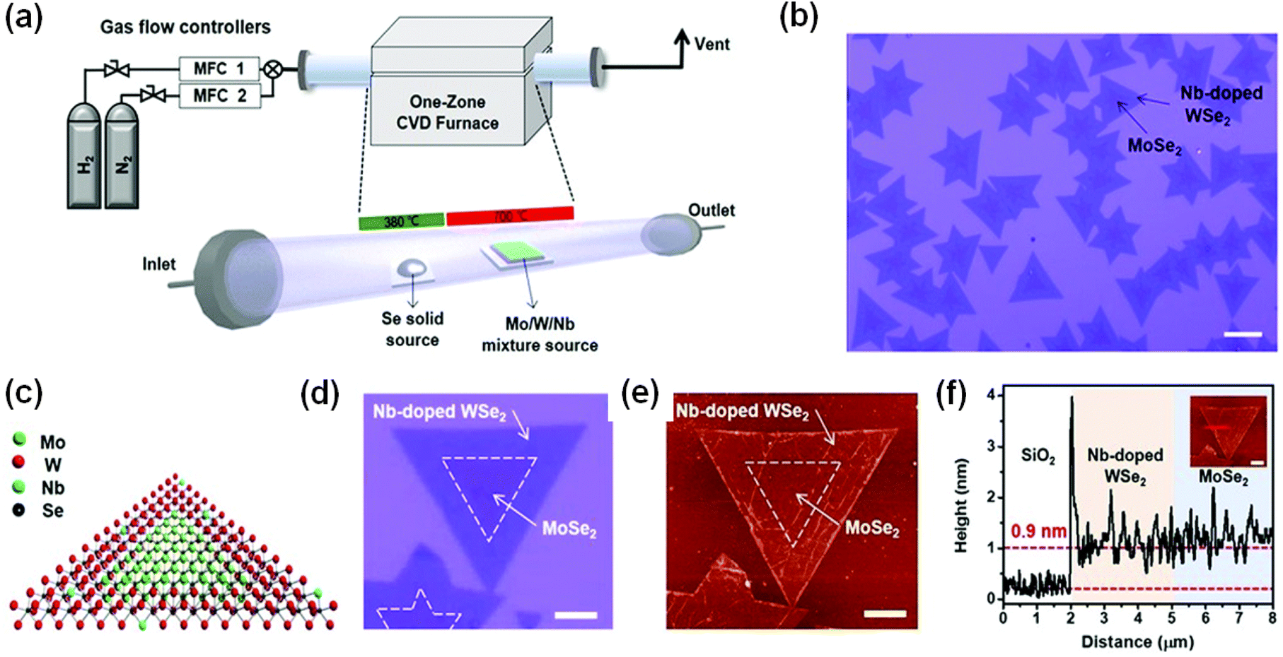 | ||
| Fig. 3 (a) One-step chamber arrangement for direct CVD development of the Nb-doped WSe2-MoSe2 p–n structure is depicted schematically. Gas concentration is regulated using a mass flow controller (MFC). (b) Image of an Nb-doped WSe2–MoSe2 based on various p–n structures with an optical microscope. The scale bar is 10 μm. (c) An in-plane heterostructure flake is observed schematically. A magnified optical microscopic picture, with a scale bar of 3 μm. (e) Image of AFM scanning and (f) height pattern along the red solid line. This shows that the flake's thickness matches the TMDC monolayer and that the flake grew as an in-plane structure. This figure is replicated by ref. 146, copyright, J. Mater. Chem. C, 2021, 9.10. | ||
2.3. Molecular beam epitaxy (MBE)
In the fields of materials science and semiconductor technology, Molecular Beam Epitaxy (MBE) is an approach used to create thin films of crystalline materials with exact monitoring of their structure and chemistry.147–151 Owing to the ultra-high vacuum used in molecular beam epitaxy (MBE), there has recently been a lot of scientific interest in the production of large-area and high-quality epilayers of different TMDCs.152–155 The fact that MBE offers several crucial competencies, including the ability to precisely regulate the composition, thickness, fundamental phases, and other features of TMDCs, makes it a perfect tool for investigating novel physics, looking into technological possibilities, and investigating basic sciences that may lead to intriguing purposes. Twenty years ago, MBE started making epitaxial TMDC films.156 By successfully growing epitaxial MoSe2 thin films and epitaxial NbSe2 thin films for the first time on a cleaved 2H MoS2 surface, Koma et al.157 accomplished ground-breaking work. Heterostructures based on 2D materials have recently been studied. Lin et al.158 presented significant advancements in thin-film synthesis and processing methods that exhibit exceptional manipulation and dependability for substitutional doping of TMDCs thin film monolayers. WTe2−xSex− and V1−xMoxSe2![[thin space (1/6-em)]](https://www.rsc.org/images/entities/char_2009.gif) 159,160 structures are among the several 2D alloys that MBE can generate with exquisite controllability. Using MBE, Ohtake et al.161 grew a heterostructure consisting of layered MoSe2 and MoTe2 monolayers (MLs) in alternating orientations. Despite the significant lattice mismatch of 6.51%, the alternately stacked MLs were produced in a nearly perfect layer-by-layer manner at least up to six MLs. The current observation has a significant meaning that the lattice mismatch also influences the structural quality of epitaxial films in the 2D materials framework.161 When the ultra-high quality of the substance's ingredients and strict control over layer thickness is necessary, MBE is recognized as a potential synthesis method for large-scale TMDC thin films and nano heterostructures.162
159,160 structures are among the several 2D alloys that MBE can generate with exquisite controllability. Using MBE, Ohtake et al.161 grew a heterostructure consisting of layered MoSe2 and MoTe2 monolayers (MLs) in alternating orientations. Despite the significant lattice mismatch of 6.51%, the alternately stacked MLs were produced in a nearly perfect layer-by-layer manner at least up to six MLs. The current observation has a significant meaning that the lattice mismatch also influences the structural quality of epitaxial films in the 2D materials framework.161 When the ultra-high quality of the substance's ingredients and strict control over layer thickness is necessary, MBE is recognized as a potential synthesis method for large-scale TMDC thin films and nano heterostructures.162
3. Techniques for generating 2D homojunctions
To further investigate fundamental features and device applications, high-quality 2D homojunction preparation is necessary. We summarized only a few methods here.163 As illustrated in Fig. 4, the described methods for fabricating 2D homojunctions may now be broadly categorized into four groups: vapor-phase deposition,164,165 lithium intercalation,166 laser irradiation,167 and doping engineering.168 Chemical doping,169 electrostatic doping,170 and photodoping171,172 are the three subcategories of doping engineering strategies based on variations in doping techniques. The ultimate kind of homojunction structure is primarily determined by applying these production techniques. Chemical doping techniques, including surface modulation, intercalation, and replacement, offer a potent and stable way to modify a semiconductor's electrical behavior. Using a local ionic gate, solid-state split gate, or ferroelectric polarization, it is often possible to modify the carrier concentration and type in distinct areas of the same material to produce electrostatic doping. The photoinduced electrons in h-BN are transferred into the channels, causing n-type doping, and this phenomenon has been frequently observed in graphene/h-BN173 and WSe2/h-BN174 heterostructures. The idea was used to build a p–n homojunction after additional development.171,172 It is noteworthy that UV light with high photon energy is typically utilized in photodoping. Heterophase homojunctions and layer-engineered homojunctions are often created via vapor-phase deposition. The fabrication of heterophase homojunction's mostly involves lithium intercalation and laser irradiation. Doping engineering methods are used to manufacture p–n homojunction.163 2D homojunction unique structures and features may provide a viable foundation for future scientific study and commercial applications. Furthermore, we anticipate that 2D homojunction's will advance rapidly as a result of the collaborative efforts of several scientific experts.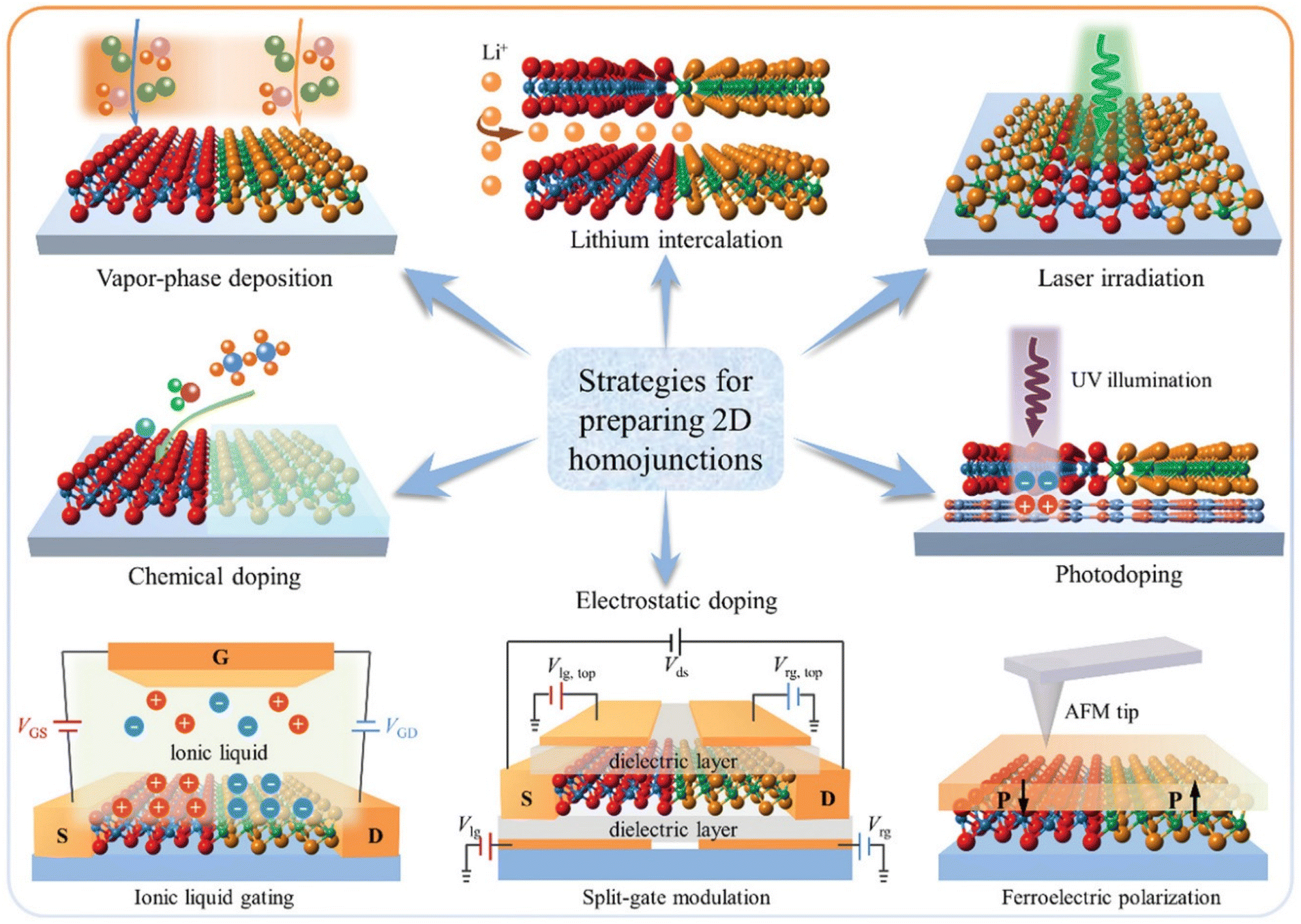 | ||
| Fig. 4 Preparation strategies for 2D homojunctions. This figure is reproduced from ref. 163, copyright, Adv. Mater.. | ||
4. Homojunctions based on TMDCs
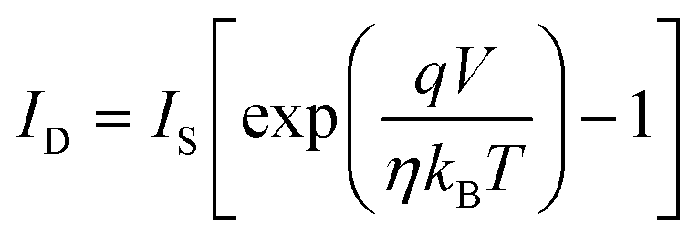
The accessibility of intrinsic p- and n-type 2D materials, such as p-type tungsten diselenide (WSe2) and n-type tungsten disulfide (WS2), is one of the main benefits of TMDCs. TMDC materials are highly desirable for a collection of applications involving FETs,175 photodetectors,176 photovoltaics,177,178 and sensors.179,180 The introduction of 2D TMDCs might address a long-standing difficulty in traditional p–n junctions built on bulk semiconductors, which have significant limits in the pursuit of low-power feasting, reduced size, and applied applications necessitating durability and versatility.181 An effective technique is to produce p–n TMDC junctions for photovoltaic device applications, in which the photoinduced electron–hole pairs may be separated swiftly.182 Building vertical heterojunctions with separated p and n TMDCs by vdW's bonding is a common method for forming p–n junctions.183 2D WSe2 has considerable promise in producing a p–n interface for next-generation photovoltaic devices because of its strong light absorption and distinctive band formation, which permits straightforward bipolar manipulation of the carrier type.184,185 Surface charge transfer is an excellent way to alter the electrical characteristics of TMDCs by efficiently convincing a change in the Fermi level to accomplish the alteration from p- to n-type carriers in low-dimensional TMDCs. Cetyltrimethyl ammonium bromide (CTAB) solutions are extensively utilized in the preparation of innovative hybrid nanomaterials for various applications, including photoluminescence, photocatalysis, battery, and photovoltaic cells as traditional and economical active substances.Hence, the improved WSe2 p–n junction is specifically created with fewer trap states in the junction system. The devices showed significant performance with a ratio (Ilight/Idark) of ≈105, a value of R of 30 A W−1 (7989% EQE), and a D* of more than 1011 Jones. The electrical characteristics, including mobility, ON-current, and threshold voltage, were carefully regulated by altering the CTAB's immersing time. These findings point to an effective method for achieving adjustable doping of 2D materials, as well as the prospective uses of WSe2 in various p–n junction-based electronic devices, such as tunnel diodes, LEDs, photodetectors, and solar cells. The schematic of the device is demonstrated in Fig. 5(a). To attain the p–n junction, half portion of the WSe2 is capped by spin-coated PMMA to avert electron doping and preserve the pristine hole characteristics; however, the remaining channel is adsorbed with CTAB to attain n-type doping. After that, the p–n junctions made of WSe2 are immersed in the CTAB solution for 2 hours to ensure that CTAB molecules are efficiently adsorbed. The inset of Fig. 5(b) displays the optical microscope image of the device after doping. The I–V> curves of the pristine and CTAB-doped devices show that the CTAB-doped WSe2 exhibits an extraordinary rectifying conduct with the ratio (Iforward/Ireverse) of approximately 103 as opposed to the essentially symmetrical structure of the pristine one, revealing an appropriate p–n diode arrangement. The Shockley diode equation is used to determine the ideality factor η of the p–n junction to assess the diode property:
 | (1) |
 | (2) |
 | (3) |
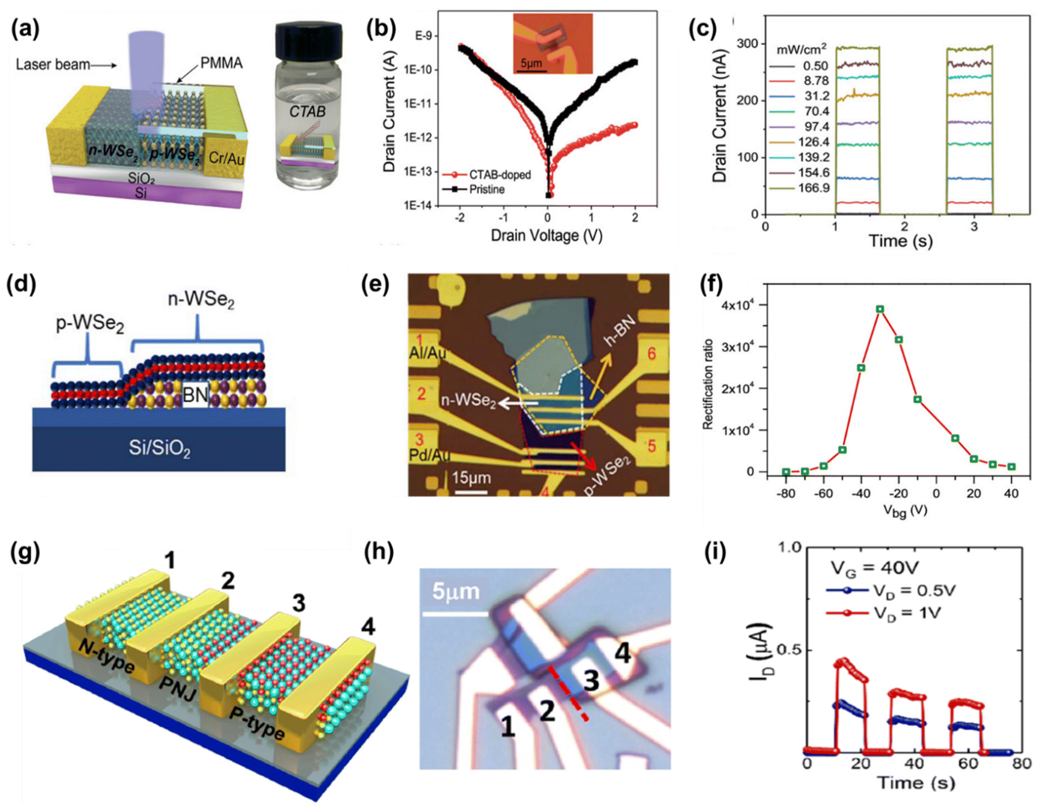 | ||
| Fig. 5 (a) Constructed WSe2 p–n junction schematic view with light illumination; the inset displays the doping technique. (b) Pristine and CTAB-doped p–n junction log-scale I–V> curves, and the device's optical microscope image are presented in the inset. (c) Summarized photocurrent data over time. These figures (a–c) are reproduced with the permission of ref. 193, copyright, Adv. Mater. (d) Schematic representation of a device based on homojunction WSe2 flake. (e) WSe2-based homojunction p–n diode optical image. (f) Rectification ratio of the WSe2-based homojunction device as a function of Vbg. These figures (d–) are reused with the permission of ref. 204, copyright, ACS Appl. Mater. Interfaces, 2020, 12.37. (g and h) Optical image (right side) and 3D graphic (left side) structure of a WSe2 FET device undergoing treatment with O2 plasma are displayed. Channels 1–2, 2–3, and 3–4 are indicated as n-WSe2, pn-WSe2, and p-WSe2. (i) Time-dependent analyses of the photocurrent in the p–n device were made with 532 nm laser illumination at fixed Vg = 40 V. These figures (g–i) are replicated by the reference,96copyright, Nanoscale 2023, 15.10. 4940–4950. | ||
Future electrical and optoelectronic applications can successfully create planar homojunction devices using the suggested doping approach without the need for a photoresist. The schematic of the purposed device is demonstrated in Fig. 5(d), where a part of the WSe2 layer was placed on the h-BN flake and a remaining portion of WSe2 was placed on the Si/SiO2 substrate. Fig. 5(e) shows a representation of the optical image of the fabricated device that contains the p–n homojunction based on WSe2. A lateral WSe2 p–n diode's rectifying performance was assessed by changing the Vbg from −80 to +40 V. The diode current significantly falls in the reverse bias when Vbg increases from −80 to −30 V, leading to an increase in the rectification ratio of up to 3.9 × 10⁴, as illustrated in Fig. 5(f). This device showed better performance compared to previous reports using other doping approaches, such as chemical doping.191,192
Conventional silicon (Si) microelectronic doping strategies are inappropriate with atomically thick 2D TMDCs, making them difficult to construct high-quality 2D homogenous p–n junctions. WSe2 is an interesting 2D material with bipolar transport properties and thickness-dependent band gaps of 1.7 eV (direct, monolayer) and roughly 1.2 eV (indirect, multilayer), in addition to predicted electron and hole motilities of around 250 and 270 cm2 V−1 s−1, respectively.193–195 Owing to its distinct physical characteristics, WSe2 has made it possible to create an extensive range of electronic and optoelectronic devices with high-quality optoelectronic performance. The application of WSe2 optoelectronic devices has recently been very interesting in novel artificial configurations based on vdW's vertical heterojunctions or lateral p–n heterostructures.184,193,196,197 In a previous study, Jo and colleagues showed that a triphenylphosphine n-doping technique significantly increased the photoresponsivity of WSe2/h-BN-based p–n heterojunction.198 A WSe2-ZnO p–n heterojunction photodetector constructed by fusing p-type WSe2 and n-type ZnO had an ultra-high value of R of about 4.83 × 10³ A W−1 under 405 nm light irradiation according to Guo and colleagues.199 According to Liu et al., under 633 nm irradiation, a photodetector based on a WSe2–Bi2Te3 p–n heterojunction may provide a quick reaction time of ∼210 μs and a suitable value of R of about ∼20.5 A W−1.139 These findings show that the effective creation of heterojunctions can substantially enhance the photoresponse properties of TMDC-based devices. Conversely, these devices still struggle with inevitable residues and are problematic in accurately localizing target materials onto the complex flake alignment procedures of other flakes. Additionally, a vdW gap among junctions may prevent carrier charge transport, which is usually unwanted for device efficiency. As a substitute technique, homogeneous junctions provide neat and self-aligned interfaces, which have inherent advantages over heterogeneous junctions. Numerous doping schemes and electrical tuning techniques, such as work function engineering methods, have been investigated in an effort to conquer the inherent performance limitations of 2D TMDCs and fix the contact issues on WSe2 functional devices.200–202 These techniques, however, are quite difficult and require high temperature or vacuum process conditions, seriously restricting their practical use in the manufacture of high-performance WSe2-based devices. Transition metal oxides (TMOs) have recently been proven to be efficient p-type contacts and dopants in organic circuitry and 2D material-based devices.203 The manufacturing of a 2D TMDC p–n homojunction with low Rc is still constrained by technical issues despite several encouraging results obtained thus far. Another approach, by applying O2 plasma treatment, was possible to readily allow the development of hole transport and therefore attain in situ p-type semiconductor properties in WSe2. This method was shown to be effective and durable. Through the transport of electrons from the WSe2 to the top layer of oxidized WOx, the stoichiometric oxidation of WSe2 into WOx strongly generates hole doping in the neighboring WSe2. Additionally, the results showed that the hole mobility in a p-type-doped WSe2 transistor increased significantly from ∼22 to ∼157 cm2 V−1 s−1 owing to the alteration of the SB to an Ohmic contact resulting from plasma conduction. Thus, under 532 nm illumination, the since-designed p–n homojunction displays a better EQE of 228%, a superb value of R of about ∼7.1 × 10⁴ mA W−1, and a photodetectivity of ∼3 × 10³ Jones. The optical visualization (top view) and schematic representation of the constructed WSe2 device are displayed in Fig. 5(g and h). Then, under various operating conditions, these WSe2 devices underwent exposure to O2 plasma. Notably, portions designated with electrodes 1 to 2 are protected by a PMMA layer, leaving areas marked with electrodes 3 to 4 exposed for O2 plasma therapy. The O2 molecule was then adsorbed onto the upper surface of the exposing WSe2, where an oxygen atom replaced the top layer of the Se atom. On top of the WSe2 layer, the WOx layer was then created. In the O2 plasma-treated (plasma-protected) area, p-type (n-type) dominating conduction appears because of O2 plasma-induced p-doping (creation of a WOx layer on top of WSe2).
The device performance results of this approach demonstrate that it is the best way to develop high-performance p–n diode devices by operating 2D TMDCs that self-oxidize. This approach may be adapted to other TMDCs for potential multifunctional electrical and optoelectronic purposes. Here, the WSe2 p–n junction photocurrent was additionally determined at a constant gate bias of 40 V and was time- and source–drain voltage-dependent (Fig. 5(i)). The photocurrent improvement was observed under varied VD and VG situations as VG swept from +40 to −40 V. The highest photocurrent is specifically attained at a gate bias voltage of 40 V. At both the VG < 0 V and VG > 0 V sides, significant alterations in the gate-dependent photocurrent may be perceived. These findings imply that the gated electric field can successfully alter the photocurrent response. Additionally, under continuous light irradiation, it is observed that the photocurrent gradually decreases over time, suggesting potential charge-trapping effects. A 40 V gate voltage results in a greater concentration of carriers and a smaller potential barrier at the contact interface. Consequently, carriers can fill the charge trap states substantially more easily, somewhat decreasing the photocurrent. The greater value of R and EQE values additionally indicate that the plasma-treated WSe2 p–n device has strong photoresponsivity. This proposed WSe2 p–n device has a D* value of around 3 × 10³ Jones. These findings demonstrate the value of O2 plasma treatment in the progress of WSe2-based optoelectronic devices. These findings support the feasibility of generating WSe2-based optoelectronic logic purposes and the practical application of the local plasma process for WSe2 flakes to modify the electrical characteristics of WSe2. We summarized the data of various homojunction p–n developments, as shown in Table 1.
| Materials | Wavelength (λ) | Responsivity | Detectivity (D*) Jones (J) | EQE (%) | Ref. |
|---|---|---|---|---|---|
| Thin WSe2/thick WSe2 | 532 nm | 0.7 mW−1 | — | 0.1 | 205 |
| WSe2 p–n | <750 nm | 16 mA W−1 | — | 3 | 124, 185 and 206 |
| Graphene p–n | Visible | 10 mA W−1 | 2.5 | 207–209 | |
| MoS2 p–n diode | 500 nm | 5.07 A W−1 | ∼3 × 10¹⁰ | ∼1200% | 191 |
| PdSe2 | (532–1470 nm) | 53 mA W−1 | 5.17 × 10¹¹ | — | 210 |
| WSe2 | 410 nm | 11.2 mA W−1 | 4.4 × 10¹⁰ | 2.6 | 211 |
| MoTe2 | 405–1550 nm | 1200 mA W−1 | 1012 | — | 212 |
| WSe2 | 520–852 nm | 2000 mA W−1 | 7.2 × 10¹⁰ | 420 | 213 |
| WSe2 (chemical doping) | 450 nm | 30 A W−1 | 1011 | 7989 | 193 |
| WSe2 (P–I–N) | 450 nm | 0.1 A W−1 | 2.2 × 10¹³ | — | 214 |
| MoTe2 | 1260–1510 nm | 156 mA W−1 | -— | 13.1 | 215 |
| MoTe2 (P–I–N) | 400–1200 nm | 1.10 A W−1 | 3.0 × 10¹² | — | 24 |
| BP | 520–1450 nm | 1.06 A W−1 | 1.27 × 10¹¹ | 90.8 | 216 |
| MoS2 | 640–1040 nm | 7 × 10⁴ A W−1 | 3.5 × 10¹⁴ | 10 | 217 |
| MoS2 | 300–700 nm | 5.07 A W−1 | 5.0 × 10¹⁰ | ∼7000 | 191 |
5. Heterostructure p–n junctions based on 2D materials
A potential geometry for obtaining broadband photodetection using a mix of extensive-bandgap and narrow-bandgap operational elements is a heterojunction based on 2D materials. However, because air bubbles and wrinkles are bound to enter the heterojunction, it is challenging to control the interface conditions. High sensitivity, quick reaction times, and a wide response range are all essential for various applications, including optical signal reception in modems,218 image recognition in cameras219,220 and infrared temperature observation in electronic thermometers.221–223 Owing to their unique optoelectronic characteristics, 2D materials are currently a viable solution for the functional layer to achieve excellent detectivity, quick reaction times, and broad detection ranges. The heterojunction framework, which commonly combines a broader bandgap and a narrow bandgap material via a mechanical exfoliation process, is the standard configuration of 2D-based photodetectors.224,225 However, this approach cannot produce efficiency at a high rate particularly when constructing heterojunctions calls for various materials.226–228 Furthermore, the inadequate interface situations of the heterojunction, which are exactly connected to D* and reaction time, are at all times influenced by bubbles and crinkles created through the stamping process.229 Furthermore, because of the high binding energy between the multiple layers, it is typically hard to exfoliate thin flakes.230 However, a thick flake results in a reduction in the detection region and sensitivity.According to a recent study, a synthesis technique that combines exfoliation and CVD can be used to create photodetectors for GaSe/PtSe2 heterojunctions. At a 10 V bias and in the avalanche mode, the devices exhibit maximum responsiveness and detectivity, which are around 1.7 A W−1 and 3.51 × 10¹² Jones, respectively. Additionally, a quick response time of 20 μs was attained. The design of the GaSe/PtSe2 photodetector's final device construction is demonstrated in Fig. 6(a). The mechanically exfoliated GaSe sheet was first stamped with PDMS onto a Si/SiO2 substrate. Then, using conventional photolithography, a specified region was etched on GaSe for the following Pt film. However, a soft oxygen plasma phase was added before the deposition of the Pt film to produce a thin oxidation layer of GaOx that was interspersed between GaSe and Pt. The GaSe/Pt structure was then placed in a CVD system for additional selenization to create a heterojunction consisting of GaSe/PtSe2. As depicted in Fig. 6(b), the optical representation of the device shape is displayed, and the testing region includes the entire junction. As described in earlier investigations, the work function of GaSe and PtSe2 is utilized here.231–233 The GaSe energy band diagrams of /PtSe2 heterojunction were created in avalanche and self-driven modes. The schematic without bias condition is shown in Fig. 6(c). A built-in electric field pointing from PtSe2 to GaSe might be produced owing to the band alignment after contact depending on the Fermi level of GaSe and PtSe2. The built-in electric field inside the junction region may separate the photo-induced electron–hole pairs, which can then be introduced as photocurrent into the electrical circuit. After the device has reached the avalanche condition under a significant reverse bias, the separated electron–hole pairs accelerate because of the strong external electric field in preparation for another collision (Fig. 6(d)). Excellent responsiveness and quick response times are mostly due to this. The device based on the optical response properties of the GaSe/PtSe2 heterojunction device is next assessed using a 520 nm laser diode and a supercontinuum light source with a wavelength ranging from 800 to 1450 nm. As depicted in Fig. 6(e), the log-scale findings are displayed in the inset, and the I–V> curve is compared with the bias voltage from −10 V to 10 V in the dark and under 520 nm illumination. Under laser irradiation, an increase is observed at zero bias, demonstrating the device's self-driven functioning. The photocurrent demonstrates a substantial increase as the bias voltage increases. In particular, the photocurrent under reverse bias is substantially larger than that under positive bias because of the heterojunction nature at the GaSe/PtSe2 interface. The device current switches the ON–OFF rate over 1000 times at a bias of −10 V (10−9 A in the dark and 10−6 A in the light), demonstrating a high sensitivity. The heterostructure's time-resolved photocurrent characteristics at a bias of −10 V are demonstrated in Fig. 6(f) by modulated light. It is possible to distinguish between “ON” and “OFF” currents, exhibiting high repeatability and stability. As demonstrated in Fig. 6(g), photocurrent switching tests using various laser wavelengths are carried out to display the broadband photoresponse at the NIR waveband. The supplied reverse-bias voltage may divide and drift the photo-generated carriers in the PtSe2 layer (bandgap: ∼0.1 eV), which are subsequently collected by the counter electrodes. One could anticipate that a PtSe2-based device will optically respond to IR light because multilayer PtSe2 has a thickness-dependent and small band gap. This research indicates that the device has a relatively low response at 1550 nm. The device displayed a quick reaction time of 20 μs and a wide photodetection range of 405–1550 nm. Additionally, an image sensor's potential has been demonstrated with respectable resolution in work. To establish a favorable junction requirement for the next advancement of electrical and photoelectric attributes, this heterojunction manufacturing approach offers an alternate choice. One of the most interesting future directions in this field is researching approaches to multifunctional vdW heterojunction devices. GeAs/ReS2 heterojunction, which is achieved here by varying the doping amount of GeAs, serves various purposes in forward rectifying diodes. The GeAs/ReS2 forward rectifying diode demonstrates extremely sensitive photodetection in a broad spectrum of up to 1550 nm, which corresponds to a short-wave infrared (SWIR) zone. Additionally, the heterojunction displays significant polarization-sensitive photodetection performance with a dichroic photocurrent ratio of 1.7 because of two robust anisotropic materials, GeAs and ReS2. The fabricated device schematic vertically stacked ReS2/GeAs vdW heterojunction is presented in Fig. 6(h). AFM was performed to determine the heterojunction's thickness; GeAs and ReS2 had thicknesses of 8.4 and 11.2 nm, respectively, equivalent to 10 and 15 layers, respectively. The AFM image is illustrated in Fig. 6(i). Optoelectronic characteristics were explored in the structure of GeAs/ReS2-based devices. Under the light of a laser with 532, 638, and 1550 nm wavelengths, the photoresponse was examined. The authors obtained the power-dependent R, EQE and D* of the heterojunction detectors illuminated by a 532 nm laser to thoroughly assess the photoelectric efficiency. The value of responsivity for that device was about 6.86 × 10³ mA W−1. Fig. 6(j) depicts EQE at various powers of incident light, which may reach 1639%. D* is a crucial parameter to reflect the least detectable signal and is equal to 1.2 × 10⁹, showing improved weak signal detection performance. This research suggests a useful technique for a multipurpose design vdW heterojunction device that will render applications in practice much easier.234 We summarized the comparative analysis of the p–n junction established on various 2D materials, as represented in Table 2.
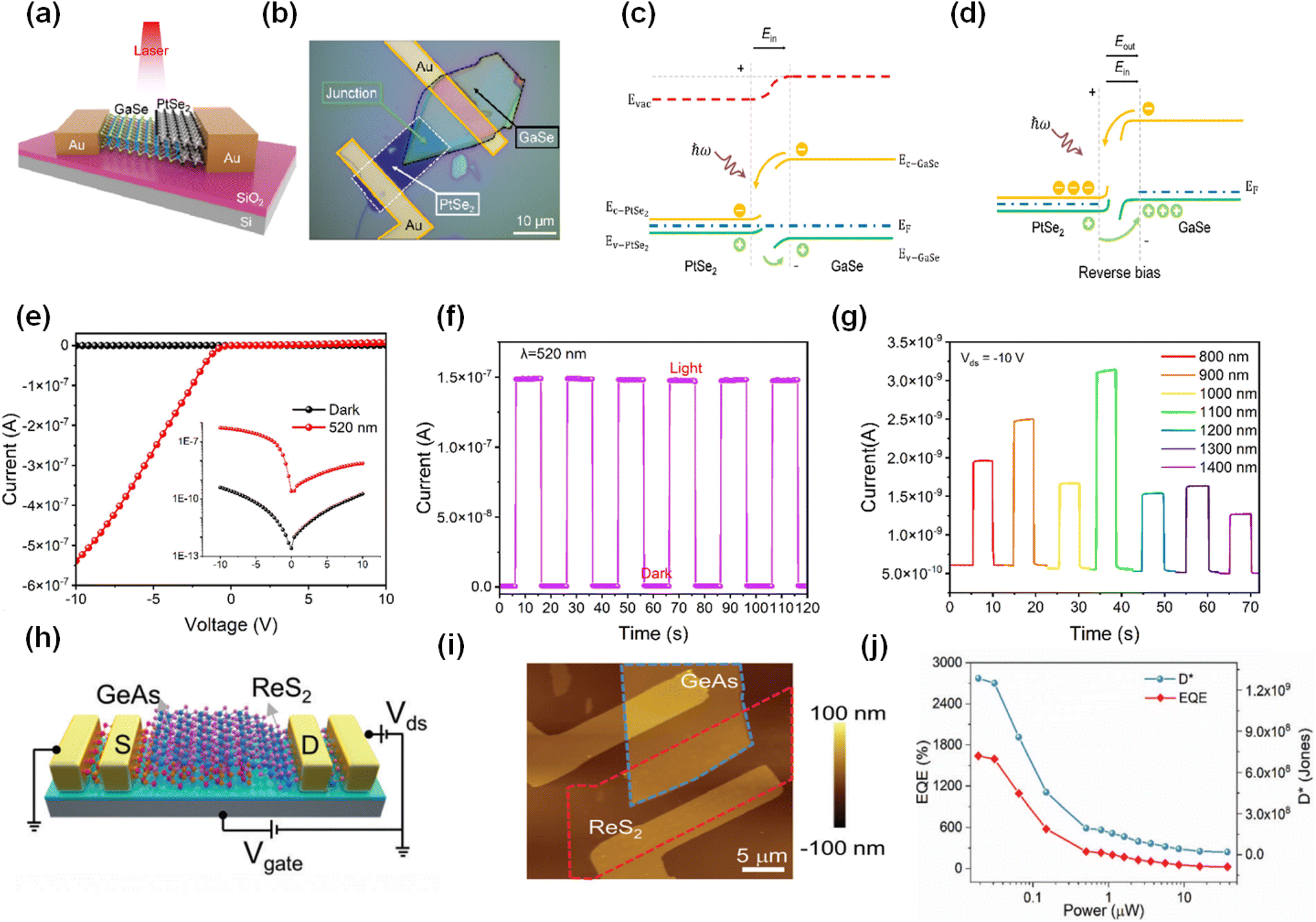 | ||
| Fig. 6 (a) Schematic p–n made of GaSe/PtSe2 in 3D form. (b) Optical image of the p–n-based photodetector. (c) GaSe/PtSe2 energy band diagram schematic. (d) Energy band diagram schematic when a reverse voltage is applied. (e) I–V> properties in the presence of visible 520 nm laser illumination (red) and complete darkness (black). (f) Test of the switching cycle of a laser using a 520 nm laser and a −10 V bias voltage. (g) Heterojunction photodetector broad response. This figure is replicated from ref. 219, copyright, Mater. Design 2023, 228. (h) Schematic illustration of GeAS/ReSe2 junction-based device. (i) AFM image of the device based on GeAs/ReS2 heterostructure, where both flakes are marked by dotted lines. (j) EQE and D* depend on power. Figures (h–j) are reproduced with the permission of ref. 234, copyright, Small, 2023. | ||
| Materials | Wavelength (λ) | Responsivity | Detectivity (D*) Jones | EQE (%) | Response time | Ref. |
|---|---|---|---|---|---|---|
| GaSe/PtSe2 | 520 nm | 1.78 A W−1 | 3.5 × 10¹² | 405 | 20 μs | 219 |
| GaSe/WS2 | 410 nm | 149 A W−1 | 4.3 × 10¹² | 450 | 37 μs | 235 |
| WSe2/ReS2 | 600 nm | 3 A W−1 | 8.39 × 10¹⁰ | 600 | 5 μs | 197 |
| BP/MoS2 | Near IR (532 nm) | 22.3 A W−1 | 3.1 × 10¹¹ | ∼1000 | 15 μs/70 μs | 236 |
| GaSe/SnS2 | 633 nm | ∼35 A W−1 | 8.2 × 10¹³ | 62 | — | 123 |
| ReS2/Te | 458 nm | 3 × 10⁶ AW−1 | 1 × 10¹¹ | 3 × 10⁴ | — | 102 |
| WSe2−MoS2 | 872 nm | 2700 A W−1 | 5 × 10¹¹ | — | 10 ms | 119 |
| p-GeSe/n-WS2 | 850 nm | 845 mA W −1 | 3.28 × 10⁸ | — | 10 ms/14 ms | 120 |
| WSe2/SnS2 | 520 nm | 108.7 A W−1 | 4.7 × 10¹⁰ | — | 500 μs/600 μs | 237 |
| MoTe2/MoS2 | 550 nm | 0.26 A W−1 | — | 58.7 | 0.2s/0.1s | 238 |
| In2Se3/GaN | 365nm | ∼70 mA W−1 | ∼1011 | ∼30 | 0.2s/0.42s | 239 |
| PtTe2/Si- | 980 nm | 406 mA W −1 | 3.62 × 10¹² | — | 2.4/32 μs | 240 |
| ReS2/MoS2 | 532–785 nm | 0.197 A W−1 | 1012 | 35% to 39% | 13/15 μs | 241 |
| PtSe2/GaAs | 200–1200 nm | 0.262 A W−1 | 2.52 × 10¹² | — | 5.5/6.5 μs | 233 |
| MoS2/CdTe | 200–1700 nm | 0.036 A W−1 | 6.1 × 10¹⁰ | — | 0.043/0.082 (ms) | 242 |
| WSe2/SnSe2 | 532–1550 nm | 588 A W−1 | 4.4 × 10¹⁰ | 1367 | 13/14 (ms) | 243 |
| WSe2/SnS2 | 550 nm | 244 A W−1 | 1.29 × 10¹³ | — | 13 (ms) | 244 |
| GaTe/InSe | 532–1550 nm | 1.5 A W−1 | 1014 | — | 360 (ms) | 245 |
| PdSe2/MoS2 | 532 nm | 600 A W−1 | 1011 | — | 100/37 (ms) | 246 |
| BP/WSe2 | 400–1550 nm | 103 A W−1 | 1014 | ∼106 | 0.8/0.8 (ms) | 247 |
| GeAs/ReS2 | 532 nm | 6.86 × 10³ mA W−1 | 1.2 × 10⁹ | 1639% | 20/30 s | 234 |
| 1550 nm | 1.02 × 10² mA W−1 | 2.16 × 10⁸ | 96/98 ms | |||
| GaSe/MoS2 | 520 nm | 0.67 A W−1 | 2.3 × 10¹¹ | ∼160% | 1.4 s | 248 |
6. P–I–N junction based on 2D materials
Recently, many methods have been used to alter conduction polarity, producing a homogenous p–n junction.191,206,249 A MoTe2-based device with a thickness on the order of nanometers may be used for short-wave infrared (SWIR) recognition in the range of even more than about 1100 nm, which is a wavelength range that Si-based devices cannot adequately report. This is because MoTe2 has a smaller bandgap (1 eV) compared to Si. This detection might be crucial in demonstrating the value of 2D-layered TMDCs over Si-based sensors for light.250–255 The recognition of visible to 1300 nm IR photons by a MoTe2 PIN junction diode is reviewed herein. Initially, p-type thin MoTe2 with 2D-like characteristics was selectively H-doped to create a p–n junction. The p–n diode also features split gates to independently regulate the EF level of the p and n regions. Therefore, by varying the gate voltages, three distinct areas of P+, virtually intrinsic (I), and N+ conduction may be created. In this case, the intrinsic (I) region develops because the split gate generation of P+ and N+ regions leads to further hole and electron depletion close to the pre-existing p–n junction, which previously had a depletion area from electron–hole recompense. For instance, the original p–n junction mode's response in the 1300 nm SWIR region is insufficient, but the response in the PIN junction diode regulated by two split gates increases by an order of magnitude. Although there have been few investigations of PIN structures in a thin TMDC semiconductor that resembles a 2D,189,254,256,257 it is generally known and comprehensible that PIN diodes have better responsiveness than p–n diodes in general elements of device physics. Fig. 7(a) displays an optical microscope image of our MoTe2-based PIN diode with two splitting gates (gate voltages: VGN and VGP) for the N+ and P+ regions, respectively, at the top and bottom of the device. Fig. 7(b) shows a 3D representation of a PIN device with a 50 nm thick ALD Al2O3 gate insulator made on a glass substrate using dry transfer and standard photolithography. The n-MoTe2 area is achieved using the top 30 nm thick ALD layer and a Ti contact for the n terminal,258,259 whereas the thin p-MoTe2 region contains Pt contact electrodes, and the p-polarity is improved via polymer CYTOP deposition. The p–n and PIN working modes of our MoTe2 photodetector are shown graphically in the schematic band diagram (Fig. 7(c)). The p–n mode requires two terminals and simple reverse-bias conditions to work, but the PIN mode combines VGP and VGN to generate P+, N+, and I regions. Based on the gate patterning, the I region comprises a small gap (<1 μm). Consequently, compared to a simple p–n junction, this area is exposed to a greater electric field when biasing is reversed. The remarkable value of R of the PIN-mode MoTe2 for 1300 nm SWIR photons is this study's most intriguing finding. Fig. 7(d) and (e) display photoinduced current plots for the p–n mode for 1300 nm SWIR radiation with no gate voltage (VGN = VGP = 0 V) as a dependence on Va and optical power density. VOC and ISC for the p–n mode are almost zero, but at larger reverse voltages, a modest photocurrent is observed. However, in PIN-mode operation, VOC, and ISC are clearly attained at 0.25 V and 50 pA, and a much-improved photo I–V> trend is monitored with varied optical power density. The PIN mode (gating) exhibits a photocurrent and R larger than those of the p–n mode (GND) at a Va of −1.5 V according to the photocurrent vs. power density visualizations displayed in Fig. 7(f). The 1300 nm SWIR area with a far larger response in the PIN mode than anticipated is still a mystery. It is strongly hypothesized that the Franz–Keldysh effect might cause a decrease in the bandgap in MoTe2. When the bandgap of 7 nm thick MoTe2 is about 0.95 eV, or the energy at a wavelength of 1300 nm, efficient absorption always requires an Eg less than 0.95 eV. Thus, the SWIR laser photons at 1300 nm may not be successfully gripped by the material. Because of the Franz–Keldysh effect, it is predicted that Eg may drop if a strong E-field were applied to the same thin MoTe2.260 In fact, even for the p–n mode, a slightly greater responsivity is produced at a reverse voltage of Va = −1.5 V than at Va = 0 V. The Eg of MoTe2 may be lowered below 0.95 eV (hvFK) owing to the introduction of a considerably higher E-field in the “I” region of the PIN diode, leading to the efficient absorption of 1300 nm SWIR photons there. We thus conclude that the PIN diode with two split gates, which exhibits greater responsiveness over the full detection range, is innovative and significant for the recognition of 1300 nm SWIR light. Herein, we review a multilayer WSe2 diode based on a lateral PIN homojunction.214 The photodiode is manufactured using particular doping; more precisely, the contact areas are treated with self-aligning surface plasma, while the WSe2 channel is left intrinsic. Electrical testing of such a diode indicates a perfect rectifying behavior with an ideality factor of 1.14 and a current on/off ratio as high as 1.2 × 10⁶. The diode exhibits good photo-detecting capabilities when working in the photovoltaic mode under 450 nm light irradiation, with a Voc of 340 mV, R of 0.1A W−1, and a D* of 2.2 × 10¹³ Jones. The lateral PIN design also considerably reduces slow photoresponse dynamics, such as photocarrier diffusion in undepleted areas and photocarrier trapping/de-trapping caused by doping process-induced defect states. Fig. 7(g) generally depicts the final constructed device's three-dimensional structure. The devices described in this study used self-aligned surface plasma processing before metal contact deposition to use the WOx and WSe2−y interfacial layers as p-type and n-type dopants separately. A 2 mm diameter homogeneous circular light point lit the entire device region. The output curves, as shown in Fig. 7(h), clearly demonstrate an increase in the current when illuminated. The output characteristics show a significant nonzero Isc at zero bias voltage when compared with the dark situation curve, with 3.3 mW cm−2 light illumination yielding a peak value of 0.57 μA. The time-dependent photoresponse was elaborated with 450 nm radiant light, and the rise and fall times are represented in Fig. 7(i), as 264 ns and 552 ns, respectively. This study indicates a significant field for fabricating p–i–n interfaces based on TMDCs by attaining selective doping using a simple applied plasma treatment approach.214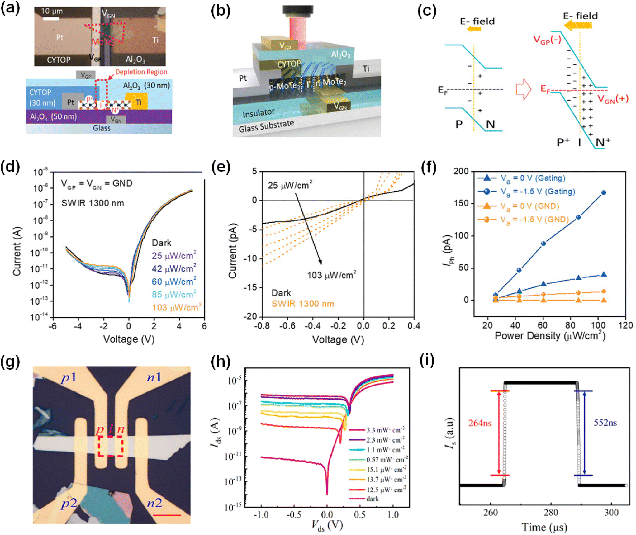 | ||
| Fig. 7 (a) MoTe2 PIN diode optical microscope photograph and cross-sectional schematic. (b) PIN diode schematic in three dimensions. (c) Schematic band diagrams for the PN and PIN operation modes. (d) Photoinduced logarithmic I–V> curves of the device for the p–n mode at different power densities with a wavelength of 1300 nm. (e) Linear scale representation, which denotes the Isc and Voc. (f) Photocurrent Iph is enhanced with radiant laser power. The blue (PIN mode) and orange (p–n state) traces demonstrate that the PIN mode's photoresponse is significantly greater than that of the p–n state. (f) Photocurrent as a function of power intensity. These figures (a–e) are replicated from ref. 261, copyright, Adv. Opt. Mater. (g) Optical image demonstration of a PIN device based on homojunction WSe2. The scale bar is 10 micro-meters. (h) WSe2 PIN junction diode's output characteristics under 450 nm irradiation as the power density varies. (i) Extended photoresponse curve at 20 kHz indicating the rise time (τr) and fall time (τf). The figures (g–i) are reproduced with the permission of ref. 214, copyright, ACS Nano. | ||
7. Broken gap p–n junction for fast photoresponse
The broken-gap vdw's heterostructure consisting of 2D material favorable for manufacturing fast tuning and low-power consumption appliances acknowledges its charge transfer vs. quantum tunneling phenomenon. Recently, broken gap vdW heterostructures (vdWHs) constructed on multiple SnSe2 and other 2D material combinations have been created using various tuning techniques (chemical doping, gating coupling, and modification of thickness).262–264 These heterostructure devices have received attention because of the tunneling processes they possess, which may be utilized to create Esaki diodes and hetero-tunnel field effect transistors (hetero-TFETs).264,265 However, the interface consisting of SnSe2 has a wide depletion zone that often hinders operational gain because SnSe2 has poor mobility and low carrier concentration.262,265 When compared to SnSe2, BP has higher mobility and higher hole carriers,266 making it an excellent channel material for creating broken gap vdWHs. Consequently, devices produced from 2D BP are becoming increasingly desirable.267,268 To build multivalued logic and binary inverters, for instance, broken-gap vdWHs made of MoS2 and BP have been constructed for particularly effective properties with a similar rectification ratio (5 × 10⁵) and high current on/off ratio (107).268 However, BP experiences ecological instability. Additionally, for a vdWH heterodiode, a VB or CB offset among the two stacking materials affects the rectifying operation in addition to the Fermi level.268 However, the aforementioned vdWH frequently has a very tiny CB offset in which the forward and reverse currents simultaneously grow, limiting the rectification ability of the device. Additionally, a photodetector's enhanced drain current results in a significant dark current, which further lowers the ratio of photocurrent on to photocurrent off.101,269We considered a broken-gap vdWH that formed a significant CB offset to block forward current by combining a thick n-type PtS2 with a thin p-type WSe2.270 Consequently, the heterodiode's rectification ratio may be significantly improved. Through photo-dominated tunneling transport, the forward photocurrent may be substantially enhanced under low illumination. Additionally, its photogenerated tunneling electrons may easily mix with the opposing majority hole carriers in the WSe2 accumulation zone, thereby reducing the interface trapping effect and considerably enhancing the reaction speed. Fig. 8(a) illustrates a schematic of a PtS2–WSe2-based broken gap heterojunction device under illumination. Fig. 8(b) displays the heterodiode device's Ids–Vds properties on a logarithmic scale at different gate voltages. The amazing thing is that an evident backward diode was created using ultralow forward currents of less than 0.2 pA and extremely large reverse currents of up to 20 μA. Thus, an extremely high reverse rectification ratio of close to 108 may be estimated using the reverse-to-forward current ratio. This heterodiode had a greater rectification ratio of many orders of magnitude when compared to previous reverse diodes made using traditional bulk materials and other 2D materials, as described in previous studies.271–274 The surface potential across PtS2 and WSe2 was measured using Kelvin probe force microscopy (KPFM) to better comprehend the tunnel operation of the PtS2/WSe2 broken gap vdWH heterodiode. According to the KPFM finding, when PtS2 and WSe2 were arranged together, the WSe2 electrons flowed into PtS2 and attained an equilibrium state, creating more electrons in PtS2 and holes in WSe2. Owing to the formation of the bilateral accumulation zone at the interface, broken-gap band alignments with significant band bending may emerge. Fig. 8(e) illustrates how, at a low negative bias, electrons move from a WSe2 valence band maximum (VBM) to a PtS2 conduction band minimum (CBM) via band-to-band tunneling (BTBT). The thick PtS2, which has mobility, can act as a useful carrier-selective contact, which helps to increase the reverse current. As shown in Fig. 8(d), if the negative bias voltage is increased, the energy band of WSe2 continues to increase and the energy band of PtS2 decreases, creating a wide tunneling window and a greater reverse current. The decrease in the energy band of WSe2 and the increase in PtS2 cause the tunneling window to disappear when a positive bias voltage is applied. Meanwhile, extreme band bending (Fig. 8(f)) restricts hot carrier emission. Thus, with a positive bias voltage, ultrasmall forward currents may be achieved. Additionally, the approximate formula for the tunneling current likelihood in 2D materials is
 | (4) |
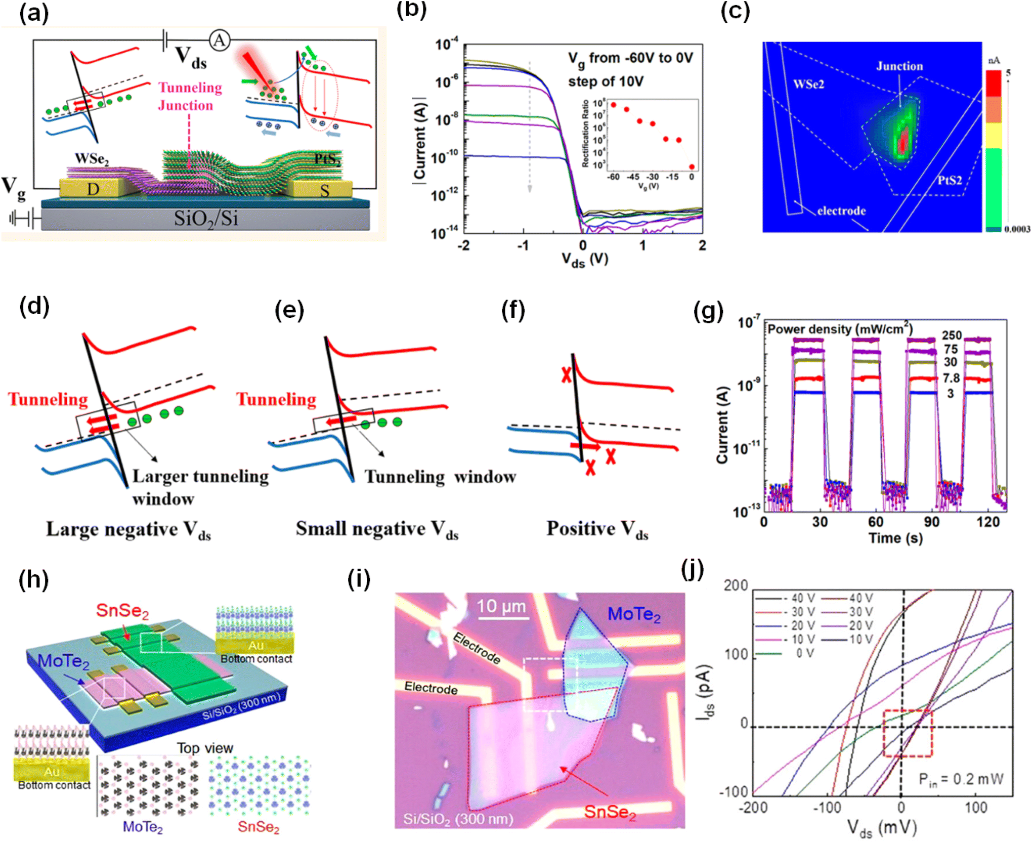 | ||
| Fig. 8 (a) Schematic representing the tunneling diode based on broken gap Vdw's heterojunction (PtS2–WSe2). (b) Idsvs. Vds curves with respect to gate voltages in logarithmic scale. (c) Scanning photocurrent mapping with a laser wavelength of 532 nm at Vds = 0 and Vg = 0. (d–f) Energy band diagram at different biases of voltage (Vds). (g) Photo current of the heterostructure-based device. These figures (a–g) are replicated from ref. 270, copyright, ACS Nano, 2021. (h) Schematic of the device based on materials MoTe2–SnSe2. (i) Optical representation of the SnSe2/MoTe2 electronic device. (j) Photovoltaic effect based on SnSe2/MoTe2 heterostructure. Ids–Vds curves at 0.2 mW laser power at various Vgs demonstrate variability in the photovoltaic effect. This figure is replicated from ref. 277, copyright, Nano Lett. | ||
A broken gap in the heterostructures of SnSe2 and MoTe2 with gate-controlled interface topologies was explored owing to their electrical and optoelectronic features.277 This device can function as an Esaki diode and a reverse diode according to the interband tunneling current, and at room temperature, its peak-to-valley current ratio is close to 5.7. Additionally, the heterojunction displays a detectivity of up to 7.5 × 10¹² Jones when subjected to an 811 nm laser beam. The SnSe2/MoTe2 heterostructure device is schematically shown in Fig. 8(h), along with top representations of the atomic structures of 1T-SnSe2 and 2H-MoTe2.278–280 An optical representation of the SnSe2/MoTe2 heterojunction is presented in Fig. 8(i). Furthermore, the photovoltaic effect of the SnSe2/MoTe2 heterojunctions was observed. Fig. 8(j) displays the Ids–Vds curves of the 811 nm laser-irradiated device at various Vgs ranging from −40 to 40 V, illustrating its photovoltaic response. Particularly, the change in gate bias from −40 to 40 V caused the Voc to shift from −100 to 20 mV. As the built-in potentials in n-type materials are larger than those in p-type materials, the VOC (photovoltaic effect) is caused by the intrinsic potential at the p–n interface and is often detected under various drain biases. Additionally, it is noteworthy that a photovoltaic effect with a fill factor greater than 41% underscored the tremendous scope of optoelectronic applications. This work not only gives a thorough grasp of broken-band orientation and its potential uses but also exhibits outstanding performance in optoelectronics predicated on the SnSe2/MoTe2 heterojunction.
8. Self-powered p–n junction for photodetection
Polarization-sensitive detectors based on p–n have attracted increased attention as an essential application scenario owing to their suitability for light detection in complicated settings.10,11,281,282 The polarization-sensitive 2D photodetector extracts polarization information from radiant light and shields the impurity signal to progress the signal-to-noise ratio, which necessitates the application of semiconductor materials possessing an inherent photoresponse to polarized light, such as BP, GeAs, ReS2, and GeSe.283 The polarization ratio was increased to more than 22 by fabricating more BP/MoS2 heterojunction photodiodes.284 Wang et al. revealed that the unique GeSe-based polarized photodetector responded anisotropically to 532, 638, and 808 nm light, with an optimal polarization ratio of 2.16 at 808 nm.285 Furthermore, many polarized photodetectors constructed using 2D-layered materials limit themselves to the visible band, restricting their angle-dependent optoelectronic applications in the IR region.285 Furthermore, the polarization sensitivity for certain 2D materials, such as SnS and ReS2, is very low owing to their intrinsic smaller mobility and high electron–hole recombination rate.285 A heterostructure composed of multilayer GeSe and 2H-MoTe2 was developed to provide polarization-sensitive and self-powered photodetection with outstanding implementation in the near-infrared spectral range, as discussed below.121 Owing to the low bandgap of both elements, the detection spectrum ranges from visible to near-IR light (405–1310 nm) at zero bias. The device has a rapid reaction time of 26 ms at a particular near-IR wavelength of 808 nm and an excellent detectivity of 4.1 × 10¹¹ Jones. Using GeSe's anisotropic optical absorption, the resulting heterojunction device obtained substantial polarization sensitivities of 5.4 and 1.8 at 635 and 1310 nm, respectively. Using the assembly of anisotropic/isotropic 2D semiconductors, the self-powered and polarization-sensitive photoresponse in the near-IR range can allow polarization-related optoelectronic presentations in IC's. Fig. 9(a) depicts the schematic design of the GeSe/MoTe2 heterojunction device. Fig. 9(b) depicts the current–voltage (I–V>) properties of GeSe/MoTe2 vdW's heterojunctions in logarithmic and linear scales under dark conditions. This diode exhibits evident current rectification conduct with a rectification ratio of roughly 300. The ideality factor is determined to be η = 1.24, which is near to η = 1, indicating that this device has a good-quality connection and that diffusion current, not recombination current, controls the rectifying performance of GeSe/MoTe2 devices.286 The time-resolved photoresponses under visible (405 and 635 nm) and near-IR (808, 980, 1064, and 1310 nm) light stimulation were implemented to test the device's self-powered photodetection capabilities, as illustrated in Fig. 9(c) at zero bias. This demonstrates a rapid and strong photocurrent with a wide spectral coverage range of 405 nm–1310 nm. It is also notable that the photoswitching ratio in infrared light can surpass 104 owing to the ultralow dark current of less than 0.1 pA in the self-driven state. To quantify the optoelectronic performance of the GeSe/MoTe2 heterostructure, the device was evaluated using a particular near-IR light with a wavelength of 808 nm. Fig. 9(d) and (e) show the I–V> curves of the heterostructure device under 808 nm laser irradiation with an improvement in light power density from 1.25 to 437.3 mW cm−2 on linear and logarithmic scales. This GeSe/MoTe2 vdW heterojunction exhibits both a sensitive photoresponse and a significant photovoltaic effect. The photoresponse is owing to the high absorption coefficients of GeSe and MoTe2 at 808 nm light, but the substantial photovoltaic effect is caused by the built-in electric field in the GeSe/MoTe2 heterojunction's depletion zone. Both the Voc and Isc increase when an 808 nm laser with enhanced optical power density is used, as shown in Fig. 9(f), with a maximum Isc of 4.58 nA and a maximum Voc of 0.43 V attained under strong light power. The following equation is utilized: Isc = cPinλ, where Isc denotes a power law connection with a light power density (Pin), c denotes the proportionality constant and λ denotes the fitting exponent. The λ is observed to be ≈0.7, suggesting that the defect level trapping charge behavior affects the photoexcited carriers in the same way as it does in other p–n heterojunctions.287 This work produces vdW heterojunctions with low bandgaps composed of in-plane anisotropic GeSe layers and isotropic MoTe2 layers, suggesting an efficient design for self-powered, broadband, and polarization-sensitive photodetection applications.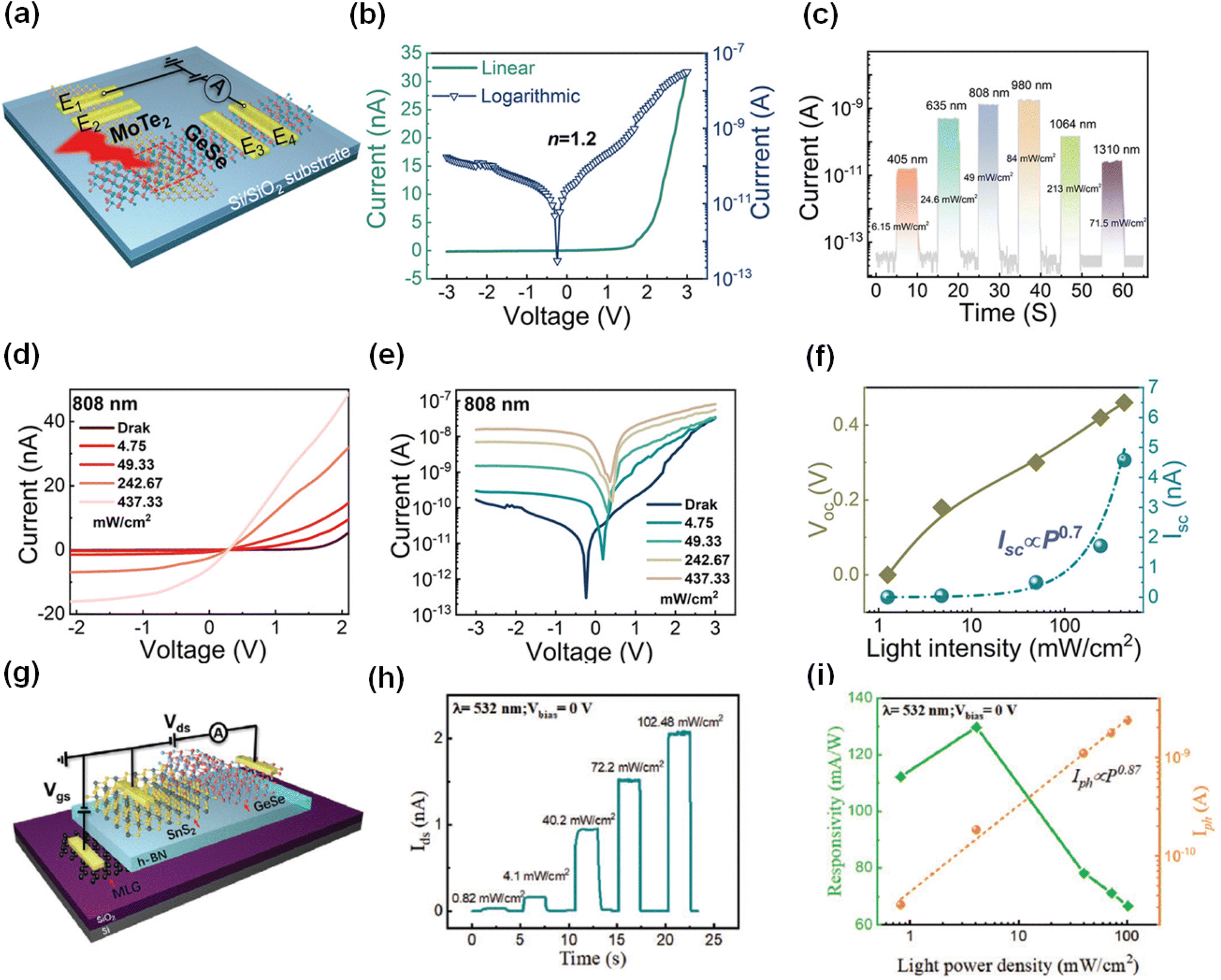 | ||
| Fig. 9 (a) Schematic design of the GeSe/MoTe2 structure-based device. (b) The I-V curve of the device is linear and log (coordinates) under dark conditions. (c) Time-resolved photoresponse of the device under multiple wavelengths of light illumination. (d) GeSe/MoTe2 heterojunction device I-V curves. (e) Logarithmic scale. At room temperature, Isc and Voc are proportional to the laser power density. (f) Voc and Isc dependency on light power density. Figure a–f is reproduced with the permission of ref. 121, copyright, Adv. Mater. Interfaces, 2022. (g) GeSe–SnS2 hetero-structured illustrated graphically in three dimensions. (h) GeSe/SnS2 photodetectors are dependent on the time photocurrent at Vbias = 0 V and various light power densities at 532 nm. (i) Consequence of light power density, the responsivity (R) and Iph/Idark ratio. This figure is replicated from ref. 288, copyright, Adv. Mater. Interfaces. | ||
Here, the vertically stacked multilayer GeSe/SnS2 design adjustable current transport and autonomous optoelectrical characteristics have been revealed.288 In addition, owing to the huge band offset and the effective carrier separation method, the device's photovoltaic characteristics include a very less dark current of 30 fA, maximum responsiveness of 130 mA W−1, and a high Ion/Ioff ratio of 105 at 532 nm. GeSe/SnS2 vdW's heterojunction-based device is shown in 3D in Fig. 9(g). Because of its increased state density, excessive charge storage ability, and the existence of charge-neutral sites (i.e., an equal number of electrons and holes), multilayer graphene (MLG) specifically serves as a bottom gate semimetal.289,290 Smooth h-BN can aid in trapping residual charges effectively and decreasing surface trap scattering compared to SiO2 with surface dangling bonds, resulting in more effective control of the transport current at less power use.291 The time-resolved photoresponse at various light power densities with Vbias = 0 V is shown in Fig. 9(h). Owing to fewer trap states at the GeSe/SnS2 junction, it can be shown that the photo-switching mechanism is robust and reproducible.286 Because of an increase in Auger recombination sites, R532 nm typically decreases in Fig. 9(i) (left axis) from 130 to 66.7 mA W−1 when the light power density increases from 4.1 to 101.48 mW cm−2. The photocurrent at 532 nm in Fig. 9(i) (right axis), which exhibits a sublinear behavior with an exponent of 0.87, is effectively fitted with a power law with the following formula: Iph ∝ Pα (where P is the radiant light power densities and the exponent defines photoelectric conversion efficiency). This shows the heterojunction's capacity to effectively transform incident photons into electron–hole pairs. The exponent α < 1 reveals that additional Auger recombination sites and trapped states affect photogenerated carriers throughout the transport period. It has been discovered that the GeSe/SnS2 vdWs device polarity-switchable conduct and self-driven photodetection ability can, hopefully, extend and improve forthcoming multipurpose-integrated devices. The summarized data related to the self-powered junction are described in Table 3.
| Materials | Wavelength (λ) | Responsivity (R) | Detectivity (D*) Jones | Response time | Ref. |
|---|---|---|---|---|---|
| GeSe/MoS2 | 532 nm | 105 mA W−1 | 1.46 × 10¹⁰ | — | 286 |
| MoTe2/MoS2 | 473 nm | 150 mA W−1 | — | 6.8 × 10⁻³ s | 292 |
| BP/InSe | 455 nm | 11.7 mA W−1 | — | 32 × 10−3 s | 293 |
| Se/WS2 | 405 nm | 196 mA W−1 | 1.3 × 10¹⁰ | — | 294 |
| SnS/InSe | 635 nm | 215 mA W−1 | 1.05 × 10¹⁰ | 4.2 s | 295 |
| GaTe/InSe | 405 nm | 13.8 mA W−1 | — | 20 × 10−3 s | 93 |
| AsP/MoS2 | 520 nm | 300 mA W−1 | — | 9 × 10⁻⁶ s | 274 |
| Te/WS2 | 635 nm | 471 mA W−1 | 1.24 × 10⁻¹⁰ | 14.7 × 10⁻³ s | 296 |
| WSe2/Ta2NiSe5/WSe2 | 635 nm | 436 mA W−1 | 0.99 × 10¹² | 0.46 × 10⁻³ s | 297 |
| WSe2/Ta2NiSe5/WSe2 | 808 nm | 37.22 A W−1 | 8.44 × 10¹⁰ | — | 297 |
| α-In2Se3/PtSe2 | 405–1550 nm | 0.08 A W−1 | 5 × 10¹¹ | 127/104 μs | 298 |
| PtTe2/MoTe2 | 635 nm | 1600 mA W−1 | 8.16 × 10¹¹ | 23 μs | 299 |
| 1310 nm | 1200 mA W−1 | 5.90 × 10¹¹ | 23 μs | ||
| SnS2/MXene Nb2C | 365 nm | 102.44 μA W−1 | 7.48 × 10¹² | — | 300 |
9. The p–n junction for flexible electronics
Owing to their remarkable qualities, 2D materials provide a foundation that enables the development of flexible functional mechanisms with a range of features. A flexible α-In2Se3/WSe2 vdW's heterostructure interaction with the piezo-phototronic effect is explored, and the device's strain-regulated photo behavior is tested.118 Owing to the noncentrosymmetric construction of the III–VI compound α-In2Se3, the strain-induced piezo-potential modifies the band slope close to the p–n junction interface, enhancing the piezo-phototronic effect's capability to separate photogenerated electron–hole pairs and their related transport features. A tensile strain of 0.433% may be used to increase the photocurrent of the device by around 18 times. Additionally, the device exhibited outstanding values of R and D*, which may be as high as 4.61 × 10⁵ A W−1 and 4.34 × 10¹⁴ Jones, respectively. These findings suggest that the strain-controlled vdW p–n hybrid junction photodetector may be made possible by the piezo-phototronic effect, which offers an innovative conception of a 2D material-based vdW heterostructure modification toward outstanding performance elastic optoelectronics.118 The schematic of the device based on the structure α-In2Se3/WSe2 is shown in Fig. 10(a). For practical uses, photoresponsivity must be independent of the intensity of the light source. However, as the data were not investigated under comparable conditions, a simple comparison of the photoresponsivity of photodetectors constructed with various architectures is inaccurate. Additionally, the following equation may be used to determine D*: D* = (Af)0.5/NEP, where A is the photodetector's functional area, f is its electrical bandwidth, and NEP is its noise equivalent power; this information is depicted in Fig. 10(b). At the lowest optical density of 0.069 W cm−2 and 0.433% tensile strain, the D* decreases under compressive strain and increases with tensile strain, which reaches the highest value of 4.34 × 10¹⁴ Jones. Under continuous on/off illumination, the device's photo-switching properties and time-dependent reliability were evaluated. The recognition of periodic switching photoresponse at zero voltage bias is shown in Fig. 10(c). The augmented Iph was achieved with a growing tensile strain, while the original Iph occurred abruptly upon the light's lighting and vanished when the light was switched off. These findings imply that the viability of vdW p–n heterostructures may be extensively extended to various piezoelectric 2D materials, which may offer guidance for producing flexible nano-optoelectronic devices with superior performance.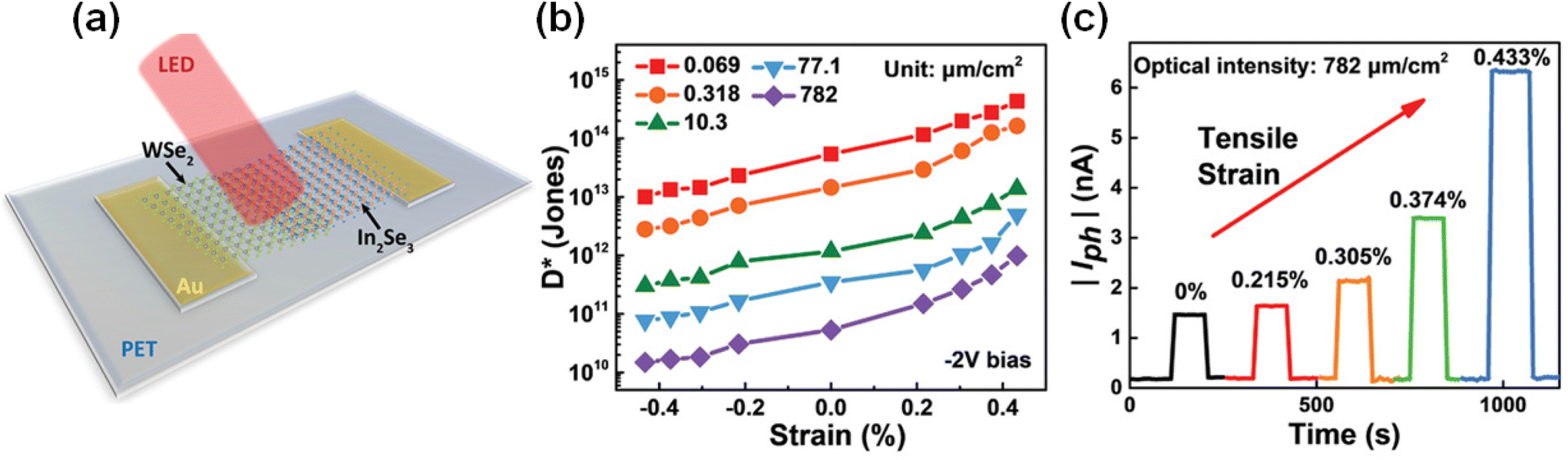 | ||
| Fig. 10 (a) Schematic illustration of the p–n diode device under red LED radiant. (b) D*'s dependency on optical power intensity under various strain settings when biased by −2 V. (c) Photoresponse evaluation in the absence of external voltage bias under irradiation of 782 W cm−2 optical intensity. This figure is replicated from ref. 118, copyright Adv. Opt. Mater., 2021. | ||
10. Challenges, solutions, and future perspectives
The development of innovative p–n interfaces in recent years has used the ultrathin structure of 2D materials. Top-down and bottom-up manufacturing processes have both been competent in producing high-quality p–n junctions with exceptional optoelectronic characteristics. We evaluated the current advances in 2D p–n junctions in this review, including the most often utilized materials and fabrication processes, as well as patterns of 2D p–n junctions from the literature to be appropriate for various distinct junction topologies. Different applications have been made possible by these designs, and we have addressed studies that employ 2D p–n junctions as rectifiers and photodetectors/solar cells, respectively. Finally, a comparison of the significant merit metrics of the various literary techniques is given. The ability to create exceptional new p–n junctions with 2D materials continues to open fascinating scientific avenues for both fundamental research and practical applications. We also conclude that the MoTe2 PIN diode with two split gates is innovative and exciting for the detection of 1300 nm SWIR radiation, demonstrating improved responsivity throughout the whole recognition range, regardless of the paucity of reports on PIN structures in 2D-like thin TMDC semiconductors. Additionally, we believe that this research may facilitate the integration of Si photodetectors on Si devices.The incorporation of 2D p–n junctions into electronic appliances still faces several obstacles despite the extensive number of studies included in this review. The manufacturing of 2D p–n devices on a wider scale and the deterioration of 2D materials owing to the environment are the two biggest obstacles. The large-scale manufacture of customized vdW's heterostructures with precise interfaces presents the first major difficulty. VdW's epitaxial techniques provide even more potential for producing 2D heterostructures of superior quality. Combining the development of single 2D materials, such as MoS2, with numerous doping processes (mainly chemical or electrostatic) provides a second potential method for increasing the construction of 2D p–n junctions. The environmental deterioration of many well-known 2D materials is a second problem. For instance, BP in its ultrathin form has the propensity to absorb moisture when exposed to air, which impairs the substance's electrical characteristics.301,302 The most widely acknowledged method for the deterioration of BP includes the material's interaction with oxygen, which modifies the material's characteristics.302,303 Encasing the air-sensitive substance among two flakes of h-BN in an environment free of oxygen and moisture is one technique to stop this deterioration.304,305 Therefore, scaling up encapsulating techniques is a focus of 2D materials research. The active search for novel 2D materials that do not have degrading issues and might originate from either synthesis (such as TiS3) or natural sources is one alternative strategy that is currently being researched (e.g. franckeite).306,307 In addition to traditional optoelectronic uses, 2D p–n junctions still have an extensive range of unanswered questions and potential applications. For instance, 2D p–n junction thermoelectric applications have not yet been fully studied. The conventional Peltier device, which is mostly used in electronics for cooling (and less often for heating), is composed of a p-type semiconductor and an n-type semiconductor thermally and electrically coupled in parallel. Combining atomically thin cooling (or heating) components with other desirable features of 2D materials, such as great transparency or flexibility, might be accomplished via van der Waals heterostructures. Another intriguing path is researching innovative p–n junction shapes (such as the recently observed circular p–n junctions in graphene308,309) or cutting-edge 2D p–n junction-based devices, such as memory or logic gates.82,268 More genuine possibilities than those mentioned are likely still concealed in 2D materials, and 2D p–n junctions have great potential for practical uses. Particularly intriguing as building blocks for flexible and transparent electrical components, such as solar cells or light-emitting diodes, are these 2D junctions.310,311 The ultrathin nature of 2D p–n junctions makes them useful for nanophotonics as well as applications in light sensing and harvesting.312,313 2D p–n junctions may be utilized as photodetectors, and several material arrangements are available that can be employed to construct devices sensitive to wavelengths spanning from the IR to ultraviolet range.236,314,315
TMDs have recently attracted significant interest because of their distinct electronic, optical, and catalytic characteristics. TMDCs are layered materials made up of chalcogen atoms and transition metal atoms sandwiched between them. They display various junctions, such as semiconductor–semiconductor, semiconductor–metal, and metal–metal junctions. TMDCs exhibit intriguing characteristics, such as superconductivity and magnetism, in metal–metal junctions. The underlying mechanisms of these phenomena have been thoroughly studied, and researchers have considered how they might be used in spintronics, energy storage, and quantum computing. TMDC-based metal–semiconductor junctions have also received considerable attention. Researchers have created novel functionalities, such as Schottky barriers, rectifying behavior, and enhanced photoresponse, by fusing various transition metals using semiconducting TMDCs. These junctions show promise for use in photovoltaics, optoelectronics, and electronic devices. Different TMDCs have been used to create semiconductor–semiconductor junctions, and these junctions have been studied owing to their potential to produce heterostructures with specialized electronic properties. Researchers have created interlayer exciton formation, bandgap engineering, and effective charge transfer by stacking layers of various TMDCs. These heterostructures offer the potential to create sensors, photodetectors, and transistors of the future.
In several critical areas, future developments in TMDC junctions are anticipated. To increase the number of feasible junctions and optimize their properties, research on new TMDC materials and their combinations will first continue. Research on novel 2D materials other than TMDCs, such as transition metal oxides and nitrides, is also included to create hybrid junctions with improved functionalities. The second goal is to comprehend the underlying physics governing TMDC junctions and to create precise theoretical simulations and models. Consequently, it is easier to predict and explain the characteristics of TMDC junctions and to design novel devices with the desired functionalities. Additionally, a significant research area is the incorporation of TMDC junctions into usable devices. The creation of functional devices with high performance and reproducibility is made possible by the development of methods for large-scale synthesis, precise positioning, and controlled alignment of TMDC layers. Additionally, the use of TMDC junctions in cutting-edge industries, such as wearable electronics, quantum information processing, and neuromorphic computing, will be investigated. TMDCs are intriguing candidates for these applications owing to their special characteristics and compatibility with flexible substrates. Finally, efforts will be focused on finding solutions for the problems that TMDC junctions face, including environmental stability, contact resistance, and scalability. TMDC junction technology will advance owing to methods for passivating TMDC surfaces, enhancing interface quality, and creating scalable fabrication techniques. Finally, recent developments in TMDC junctions have shown enormous potential for various applications. The achievement of TMDC-based devices with superior performance and new functionalities will result from continued research and development in this field.
Conflicts of interest
The authors declare no competing financial interests.Acknowledgements
The authors extend their appreciation to the Deanship of Scientific Research at King Khalid University for funding this work through a large group Research Project under grant number RGP.2/575/44.This work is also supported by the National Research Foundation of Korea (NRF) grant funded by the Korean government (MSIT) (No. RS-2022-00165798).
References
- B. Radisavljevic, et al., Single-layer MoS2 transistors, Nat. Nanotechnol., 2011, 6(3), 147–150 CrossRef CAS PubMed.
- K. F. Mak, et al., Atomically thin MoS 2: a new direct-gap semiconductor, Phys. Rev. Lett., 2010, 105(13), 136805 CrossRef PubMed.
- O. Lopez-Sanchez, et al., Ultrasensitive photodetectors based on monolayer MoS2, Nat. Nanotechnol., 2013, 8(7), 497–501 CrossRef CAS PubMed.
- J. Zhou, et al., A library of atomically thin metal chalcogenides, Nature, 2018, 556(7701), 355–359 CrossRef CAS PubMed.
- L. Li, et al., Black phosphorus field-effect transistors, Nat. Nanotechnol., 2014, 9(5), 372–377 CrossRef CAS PubMed.
- F. Xia, H. Wang and Y. Jia, Rediscovering black phosphorus as an anisotropic layered material for optoelectronics and electronics, Nat. Commun., 2014, 5(1), 1–6 Search PubMed.
- N. Tombros, et al., Electronic spin transport and spin precession in single graphene layers at room temperature, Nature, 2007, 448(7153), 571–574 CrossRef CAS PubMed.
- P. Zomer, et al., Long-distance spin transport in high-mobility graphene on hexagonal boron nitride, Phys. Rev. B: Condens. Matter Mater. Phys., 2012, 86(16), 161416 CrossRef.
- E. Elahi, et al., A review on two-dimensional (2D) magnetic materials and their potential applications in spintronics and spin-caloritronic, Comput. Mater. Sci., 2022, 213, 111670 CrossRef CAS.
- E. Elahi, et al., A brief review on the spin valve magnetic tunnel junction composed of 2D materials, J. Phys. D: Appl. Phys., 2022, 55, 423001 CrossRef.
- E. Elahi, et al., Recent advances in thermomagnetic devices for spin-caloritronic phenomena, Appl. Mater. Today, 2023, 32, 101846 CrossRef.
- E. Elahi, et al., Temperature, Bias, Angle, and Thickness–Dependent Magnetoresistance in a Vertical Spin Valve Structure CoFe/TiO2/CoFe, Phys. Status Solidi RRL, 2023, 17(2), 2200212 CrossRef CAS.
- A. C. Neto, et al., The electronic properties of graphene, Rev. Mod. Phys., 2009, 81(1), 109 CrossRef.
- T. Ando, The electronic properties of graphene and carbon nanotubes, NPG Asia Mater., 2009, 1(1), 17–21 CrossRef.
- M. W. Iqbal, et al., Enhancing the electronic properties of the graphene-based field-effect transistor via chemical doping of KBr, J. Mater. Sci.: Mater. Electron., 2022, 33(15), 12416–12425 CrossRef CAS.
- M. Iqbal, et al., Chemical doping of transition metal dichalcogenides (TMDCs) based field effect transistors: A review, Superlattices Microstruct., 2020, 137, 106350 CrossRef CAS.
- M. W. Iqbal, et al., Experimental and theoretical insights into electronic properties of oxygen-doped MoTe2 field effect transistor, Microelectron. Eng., 2022, 265, 111885 CrossRef CAS.
- F. Bonaccorso, et al., Graphene photonics and optoelectronics, Nat. Photonics, 2010, 4(9), 611–622 CrossRef CAS.
- F. H. Koppens, D. E. Chang and F. J. García de Abajo, Graphene plasmonics: a platform for strong light–matter interactions, Nano Lett., 2011, 11(8), 3370–3377 CrossRef CAS PubMed.
- E. Elahi, et al., Enhanced electrical and broad spectral (UV-Vis-NIR) photodetection in a Gr/ReSe 2/Gr heterojunction, Dalton Trans., 2020, 49(29), 10017–10027 RSC.
- M. F. Khan, et al., Bipolar Photoresponse of a Graphene Field-Effect Transistor Induced by Photochemical Reactions, ACS Appl. Electron. Mater., 2023, 5(9), 5111–5119 CrossRef CAS.
- E. Elahi, et al., Gate-Tunable Rectification and Photoresponse in a MoTe2/SnS2 van der Waals Heterostructure PN Diode, J. Mater. Chem. C, 2023, 11(40), 13981–13990 RSC.
- E. Elahi, et al., Robust approach towards wearable power efficient transistors with low subthreshold swing, Mater. Today Phys., 2022, 100943 Search PubMed.
- S. Aftab, et al., Lateral PIN (p-MoTe2/Intrinsic-MoTe2/n-MoTe2) Homojunction Photodiodes, ACS Appl. Nano Mater., 2022, 5(5), 6455–6462 CrossRef CAS.
- S. Castilla, et al., Fast and sensitive terahertz detection using an antenna-integrated graphene pn junction, Nano Lett., 2019, 19(5), 2765–2773 CrossRef CAS PubMed.
- Q. Li, et al., Ohmic contacts between monolayer WSe2 and two-dimensional titanium carbides, Carbon, 2018, 135, 125–133 CrossRef CAS.
- Q. Bao and K. P. Loh, Graphene photonics, plasmonics, and broadband optoelectronic devices, ACS Nano, 2012, 6(5), 3677–3694 CrossRef CAS PubMed.
- B. Y. Zhang, et al., Broadband high photoresponse from pure monolayer graphene photodetector, Nat. Commun., 2013, 4(1), 1–11 Search PubMed.
- A. Pospischil, et al., CMOS-compatible graphene photodetector covering all optical communication bands, Nat. Photonics, 2013, 7(11), 892–896 CrossRef CAS.
- M. Liu, et al., A graphene-based broadband optical modulator, Nature, 2011, 474(7349), 64–67 CrossRef CAS PubMed.
- P. You, et al., Efficient semitransparent perovskite solar cells with graphene electrodes, Adv. Mater., 2015, 27(24), 3632–3638 CrossRef CAS PubMed.
- L. T. Le, et al., Graphene supercapacitor electrodes fabricated by inkjet printing and thermal reduction of graphene oxide, Electrochem. Commun., 2011, 13(4), 355–358 CrossRef CAS.
- S. Cho and M. S. Fuhrer, Charge transport and inhomogeneity near the minimum conductivity point in graphene, Phys. Rev. B: Condens. Matter Mater. Phys., 2008, 77(8), 081402 CrossRef.
- F. Wang, et al., Gate-variable optical transitions in graphene, science, 2008, 320(5873), 206–209 CrossRef CAS PubMed.
- A. N. Grigorenko, M. Polini and K. Novoselov, Graphene plasmonics, Nat. Photonics, 2012, 6(11), 749–758 CrossRef CAS.
- E. Hwang and S. D. Sarma, Dielectric function, screening, and plasmons in two-dimensional graphene, Phys. Rev. B: Condens. Matter Mater. Phys., 2007, 75(20), 205418 CrossRef.
- G. Xing, et al., The physics of ultrafast saturable absorption in graphene, Opt. Express, 2010, 18(5), 4564–4573 CrossRef CAS PubMed.
- H. Yang, et al., Giant two-photon absorption in bilayer graphene, Nano Lett., 2011, 11(7), 2622–2627 CrossRef CAS PubMed.
- G.-K. Lim, et al., Giant broadband nonlinear optical absorption response in dispersed graphene single sheets, Nat. Photonics, 2011, 5(9), 554–560 CrossRef CAS.
- J. M. Dawlaty, et al., Measurement of the optical absorption spectra of epitaxial graphene from terahertz to visible, Appl. Phys. Lett., 2008, 93(13), 131905 CrossRef.
- K. F. Mak, et al., Measurement of the optical conductivity of graphene, Phys. Rev. Lett., 2008, 101(19), 196405 CrossRef PubMed.
- Y. Du, et al., Ab initio studies on atomic and electronic structures of black phosphorus, J. Appl. Phys., 2010, 107(9), 093718 CrossRef.
- C. Han, et al., Electronic structure of black phosphorus studied by angle-resolved photoemission spectroscopy, Phys. Rev. B: Condens. Matter Mater. Phys., 2014, 90(8), 085101 CrossRef CAS.
- Q. Guo, et al., Black phosphorus mid-infrared photodetectors with high gain, Nano Lett., 2016, 16(7), 4648–4655 CrossRef CAS PubMed.
- J. Miao, L. Zhang and C. Wang, Black phosphorus electronic and optoelectronic devices, 2D Mater., 2019, 6(3), 032003 CrossRef CAS.
- Y. Yi, et al., Optical and optoelectronic properties of black phosphorus and recent photonic and optoelectronic applications, Small Methods, 2019, 3(10), 1900165 CrossRef CAS.
- Y. Gogotsi and B. Anasori, The rise of MXenes, ACS Publications, 2019, pp. 8491–8494 Search PubMed.
- D. H. Ho, et al., Sensing with MXenes: progress and prospects, Adv. Mater., 2021, 33(47), 2005846 CrossRef CAS PubMed.
- M. Naguib, M. W. Barsoum and Y. Gogotsi, Ten years of progress in the synthesis and development of MXenes, Adv. Mater., 2021, 33(39), 2103393 CrossRef CAS PubMed.
- Y. Zhou, et al., Out-of-plane piezoelectricity and ferroelectricity in layered α-In2Se3 nanoflakes, Nano Lett., 2017, 17(9), 5508–5513 CrossRef CAS PubMed.
- H. Shi, et al., Ultrafast Electrochemical Synthesis of Defect–Free In2Se3 Flakes for Large–Area Optoelectronics, Adv. Mater., 2020, 32(8), 1907244 CrossRef CAS PubMed.
- X.-Z. Li, et al., Growth of vertical heterostructures based on orthorhombic SnSe/hexagonal In 2 Se 3 for high-performance photodetectors, Nanoscale Adv., 2019, 1(7), 2606–2611 RSC.
- Z. Wang and F. Pang, A facile way to control phase of tin selenide flakes by chemical vapor deposition, Chem. Phys. Lett., 2018, 702, 90–95 CrossRef CAS.
- S. Zhao, et al., Controlled synthesis of single-crystal SnSe nanoplates, Nano Res., 2015, 8(1), 288–295 CrossRef CAS.
- J. Wu, et al., Spiral growth of SnSe2 crystals by chemical vapor deposition, Adv. Mater. Interfaces, 2016, 3(16), 1600383 CrossRef.
- J. Guo, et al., SnSe/MoS2 van der Waals Heterostructure Junction Field–Effect Transistors with Nearly Ideal Subthreshold Slope, Adv. Mater., 2019, 31(49), 1902962 CrossRef CAS PubMed.
- M. Dai, et al., A dual-band multilayer InSe self-powered photodetector with high performance induced by surface plasmon resonance and asymmetric Schottky junction, ACS Nano, 2018, 12(8), 8739–8747 CrossRef CAS PubMed.
- H. Jang, et al., High–Performance Near–Infrared Photodetectors Based on Surface–Doped InSe, Adv. Funct. Mater., 2021, 31(3), 2006788 CrossRef CAS.
- E. Heidari, et al., On-chip Fourier transform spectrometer on silicon-on-sapphire, Opt. Lett., 2019, 44(11), 2883–2886 CrossRef CAS.
- E. Heidari, et al., Hexagonal transverse-coupled-cavity VCSEL redefining the high-speed lasers, Nanophotonics, 2020, 9(16), 4743–4748 CrossRef.
- A. Rostamian, et al., Towards lab-on-chip ultrasensitive ethanol detection using photonic crystal waveguide operating in the mid-infrared, Nanophotonics, 2021, 10(6), 1675–1682 CrossRef CAS.
- Z. Chen, J. Biscaras and A. Shukla, A high performance graphene/few-layer InSe photo-detector, Nanoscale, 2015, 7(14), 5981–5986 RSC.
- L. Liu, et al., Ferroelectric-gated InSe photodetectors with high on/off ratios and photoresponsivity, Nano Lett., 2020, 20(9), 6666–6673 CrossRef CAS PubMed.
- S. Aftab, et al., ReSe2/metal interface for hydrogen gas sensing, J. Colloid Interface Sci., 2021, 603, 511–517 CrossRef CAS PubMed.
- M. W. Iqbal, et al., A facile route to enhance the mobility of MoTe2 field effect transistor via chemical doping, Superlattices Microstruct., 2020, 147, 106698 CrossRef CAS.
- H. Tan, et al., Ultrathin 2D photodetectors utilizing chemical vapor deposition grown WS2 with graphene electrodes, ACS Nano, 2016, 10(8), 7866–7873 CrossRef CAS PubMed.
- F. Koppens, et al., Photodetectors based on graphene, other two-dimensional materials and hybrid systems, Nat. Nanotechnol., 2014, 9(10), 780–793 CrossRef CAS PubMed.
- M. Kang, et al., Universal mechanism of band-gap engineering in transition-metal dichalcogenides, Nano Lett., 2017, 17(3), 1610–1615 CrossRef CAS PubMed.
- Q. H. Wang, et al., Electronics and optoelectronics of two-dimensional transition metal dichalcogenides, Nat. Nanotechnol., 2012, 7(11), 699–712 CrossRef CAS PubMed.
- B. Radisavljevic, M. B. Whitwick and A. Kis, Integrated circuits and logic operations based on single-layer MoS2, ACS Nano, 2011, 5(12), 9934–9938 CrossRef CAS PubMed.
- H. Fang, et al., Degenerate n-doping of few-layer transition metal dichalcogenides by potassium, Nano Lett., 2013, 13(5), 1991–1995 CrossRef CAS PubMed.
- M. Iqbal, et al., Tailoring the electrical properties of MoTe2 field effect transistor via chemical doping, Superlattices Microstruct., 2019, 135, 106247 CrossRef CAS.
- M. W. Iqbal, et al., Improvement in electronic attributes of tungsten diselenide (WSe2)-based field-effect transistor via gas doping (DUV+ N2), J. Mater. Sci.: Mater. Electron., 2023, 34(7), 677 CrossRef CAS.
- Z. Sun, A. Martinez and F. Wang, Optical modulators with 2D layered materials, Nat. Photonics, 2016, 10(4), 227–238 CrossRef CAS.
- J. A. Tatum and J. K. Guenter, Consumer electronics with optical communication interface. 2010, Google Patents.
- G.-H. Lee, et al., Graphene-based Josephson junction microwave bolometer, Nature, 2020, 586(7827), 42–46 CrossRef CAS PubMed.
- J. F. Geisz, et al., Six-junction III–V solar cells with 47.1% conversion efficiency under 143 Suns concentration, Nat. Energy, 2020, 5(4), 326–335 CrossRef CAS.
- M. P. Levendorf, et al., Graphene and boron nitride lateral heterostructures for atomically thin circuitry, Nature, 2012, 488(7413), 627–632 CrossRef CAS PubMed.
- C. Huang, et al., Lateral heterojunctions within monolayer MoSe2−WSe2 semiconductors, Nat. Mater., 2014, 13(12), 1096–1101 CrossRef CAS PubMed.
- X. Duan, et al., Lateral epitaxial growth of two-dimensional layered semiconductor heterojunctions, Nat. Nanotechnol., 2014, 9(12), 1024–1030 CrossRef CAS PubMed.
- K. Novoselov, et al., 2D materials and van der Waals heterostructures, Science, 2016, 353(6298), aac9439 CrossRef CAS PubMed.
- D. Li, et al., Two-dimensional non-volatile programmable p–n junctions, Nat. Nanotechnol., 2017, 12(9), 901–906 CrossRef CAS PubMed.
- P. K. Sahoo, et al., One-pot growth of two-dimensional lateral heterostructures via sequential edge-epitaxy, Nature, 2018, 553(7686), 63–67 CrossRef CAS PubMed.
- X. Zong, et al., Black phosphorus-based van der Waals heterostructures for mid-infrared light-emission applications, Light: Sci. Appl., 2020, 9(1), 1–8 CrossRef PubMed.
- D. Li, et al., Light-triggered two-dimensional lateral homogeneous pn diodes for opto-electrical interconnection circuits, Sci. Bull., 2020, 65(4), 293–299 CrossRef CAS PubMed.
- H. Zeng, et al., Valley polarization in MoS2 monolayers by optical pumping, Nat. Nanotechnol., 2012, 7(8), 490–493 CrossRef CAS PubMed.
- Y. Yoon, K. Ganapathi and S. Salahuddin, How good can monolayer MoS2 transistors be?, Nano Lett., 2011, 11(9), 3768–3773 CrossRef CAS PubMed.
- X. Wang, et al., Controlled growth of SnSe/MoS2 vertical p–n heterojunction for optoelectronic applications, Nano Futures, 2021, 5(1), 015002 CrossRef CAS.
- M. Riordan and L. Hoddeson, Origins of the pn junction, IEEE spectrum, 1997, 34(6), 46–51 Search PubMed.
- C.-T. Sah, R. N. Noyce and W. Shockley, Carrier generation and recombination in pn junctions and pn junction characteristics, Proc. IRE, 1957, 45(9), 1228–1243 Search PubMed.
- R. Frisenda, et al., Atomically thin p–n junctions based on two-dimensional materials, Chem. Soc. Rev., 2018, 47(9), 3339–3358 RSC.
- M. Lee, et al., Homogeneous Palladium Diselenide pn–Junction Diodes for Reconfigurable Circuit Applications, Adv. Electron. Mater., 2022, 8(10), 2101282 CrossRef CAS.
- W. Feng, et al., A fast and zero-biased photodetector based on GaTe–InSe vertical 2D p–n heterojunction, 2D Mater., 2018, 5(2), 025008 CrossRef.
- S. Cao, et al., Ultrahigh-photoresponsive UV photodetector based on a BP/ReS 2 heterostructure p–n diode, Nanoscale, 2018, 10(35), 16805–16811 RSC.
- Y. Shan, et al., Few–layered MoS2 Based Vertical van der Waals p–n Homojunction by Highly–efficient N2 Plasma Implantation, Adv. Electron. Mater., 2022, 8(10), 2200299 CrossRef CAS.
- D. Yue, et al., Homogeneous in-plane WSe 2 P–N junctions for advanced optoelectronic devices, Nanoscale, 2023, 15(10), 4940–4950 RSC.
- A. S. Rosyadi, et al., Formation of van der Waals Stacked p–n Homojunction Optoelectronic Device of Multilayered ReSe2 by Cr Doping, Adv. Opt. Mater., 2022, 10(13), 2200392 CrossRef CAS.
- J. S. Ross, et al., Interlayer exciton optoelectronics in a 2D heterostructure p–n junction, Nano Lett., 2017, 17(2), 638–643 CrossRef CAS PubMed.
- A.-J. Cho, et al., Two-dimensional WSe2/MoS2 p–n heterojunction-based transparent photovoltaic cell and its performance enhancement by fluoropolymer passivation, ACS Appl. Mater. Interfaces, 2018, 10(42), 35972–35977 CrossRef CAS PubMed.
- S. Aftab, et al., van der Waals multi–heterostructures (PN, PIN, and NPN) for dynamic rectification in 2D materials, Adv. Mater. Interfaces, 2020, 7(24), 2001479 CrossRef CAS.
- P. K. Srivastava, et al., Multifunctional van der Waals broken–gap heterojunction, Small, 2019, 15(11), 1804885 CrossRef PubMed.
- T. U. Tran, et al., Gate tunable photoresponse of a two-dimensional pn junction for high performance broadband photodetector, Appl. Mater. Today, 2022, 26, 101285 CrossRef.
- H. Fang, et al., Strong interlayer coupling in van der Waals heterostructures built from single-layer chalcogenides, Proc. Natl. Acad. Sci. U. S. A., 2014, 111(17), 6198–6202 CrossRef CAS PubMed.
- P. K. Sahoo, et al., Bilayer lateral heterostructures of transition-metal dichalcogenides and their optoelectronic response, ACS Nano, 2019, 13(11), 12372–12384 CrossRef CAS PubMed.
- S. Berweger, et al., Spatially resolved persistent photoconductivity in MoS2−WS2 lateral heterostructures, ACS Nano, 2020, 14(10), 14080–14090 CrossRef CAS PubMed.
- P. K. Sahoo, et al., Probing nano-heterogeneity and aging effects in lateral 2D heterostructures using tip-enhanced photoluminescence, Opt. Mater. Express, 2019, 9(4), 1620–1631 CrossRef CAS.
- J. Dong, et al., The epitaxy of 2D materials growth, Nat. Commun., 2020, 11(1), 5862 CrossRef CAS PubMed.
- D. Pierucci, et al., Evidence for highly p-type doping and type II band alignment in large scale monolayer WSe 2/Se-terminated GaAs heterojunction grown by molecular beam epitaxy, Nanoscale, 2022, 14(15), 5859–5868 RSC.
- T. T. Pham, et al., Higher-indexed Moiré patterns and surface states of MoTe2/graphene heterostructure grown by molecular beam epitaxy, npj 2D Mater. Appl., 2022, 6(1), 48 CrossRef CAS.
- R. Yang and M. Sun, Borophenes: monolayer, bilayer and heterostructures, J. Mater. Chem. C, 2023, 11(21), 6834–6846 RSC.
- P. Cheng, K. Sun and Y. H. Hu, Mechanically-induced reverse phase transformation of MoS 2 from stable 2H to metastable 1T and its memristive behavior, RSC Adv., 2016, 6(70), 65691–65697 RSC.
- S. Roy, et al., Structure, properties and applications of two–dimensional hexagonal boron nitride, Adv. Mater., 2021, 33(44), 2101589 CrossRef CAS PubMed.
- L. W. Ng, et al., Structures, properties and applications of 2D materials, Printing of Graphene and Related 2D Materials: Technology, Formulation and Applications, 2019, pp. 19–51 Search PubMed.
- S. Fan, et al., Black phosphorus-based nanohybrids for energy storage, catalysis, sensors, electronic/photonic devices, and tribological applications, J. Mater. Chem. C, 2022, 10(38), 14053–14079 RSC.
- M. Zhao, et al., Advances in Two-Dimensional Materials for Optoelectronics Applications, Crystals, 2022, 12(8), 1087 CrossRef CAS.
- A. K. Geim and K. S. Novoselov, The rise of graphene, Nat. Mater., 2007, 6(3), 183–191 CrossRef CAS PubMed.
- A. Kumar, et al., Exfoliation of hematite: Morphological, structural and magnetic investigations, J. Magn. Magn. Mater., 2022, 542, 168507 CrossRef CAS.
- Y. Zhao, et al., Piezo–Phototronic Effect in 2D α–In2Se3/WSe2 van der Waals Heterostructure for Photodetector with Enhanced Photoresponse, Adv. Opt. Mater., 2021, 9(20), 2100864 CrossRef CAS.
- G. H. Shin, et al., Ultrasensitive phototransistor based on WSe2−MoS2 van der Waals heterojunction, Nano Lett., 2020, 20(8), 5741–5748 CrossRef CAS PubMed.
- S. H. A. Jaffery, et al., Thickness–Dependent, Gate–Tunable Rectification and Highly Sensitive Photovoltaic Behavior of Heterostructured GeSe/WS2 p–n Diode, Adv. Mater. Interfaces, 2020, 7(23), 2000893 CrossRef CAS.
- N. Zhang, et al., Near–Infrared, Self–Powered and Polarization–Sensitive Photodetector Based on GeSe–MoTe2 p–n Heterojunction, Adv. Mater. Interfaces, 2022, 9(15), 2200150 CrossRef CAS.
- V. M. Freire Soler , Fabrication and characterization of macroscopic graphene layers on metallic substrates. 2014.
- P. Perumal, et al., Staggered band offset induced high performance opto-electronic devices: Atomically thin vertically stacked GaSe-SnS2 van der Waals pn heterostructures, Appl. Surf. Sci., 2021, 535, 147480 CrossRef CAS.
- J. S. Ross, et al., Electrically tunable excitonic light-emitting diodes based on monolayer WSe2 p–n junctions, Nat. Nanotechnol., 2014, 9(4), 268–272 CrossRef CAS PubMed.
- F. Xia, et al., Ultrafast graphene photodetector, Nat. Nanotechnol., 2009, 4(12), 839–843 CrossRef CAS PubMed.
- Y.-H. Chang, et al., Monolayer MoSe2 grown by chemical vapor deposition for fast photodetection, ACS Nano, 2014, 8(8), 8582–8590 CrossRef CAS PubMed.
- K. F. Mak and J. Shan, Photonics and optoelectronics of 2D semiconductor transition metal dichalcogenides, Nat. Photonics, 2016, 10(4), 216–226 CrossRef CAS.
- W. Liao, et al., van der Waals heterostructures for optoelectronics: progress and prospects, Appl. Mater. Today, 2019, 16, 435–455 CrossRef.
- S.-M. Huang, et al., A Weyl Fermion semimetal with surface Fermi arcs in the transition metal monopnictide TaAs class, Nat. Commun., 2015, 6(1), 7373 CrossRef CAS PubMed.
- M.-Y. Li, et al., Epitaxial growth of a monolayer WSe2-MoS2 lateral pn junction with an atomically sharp interface, Science, 2015, 349(6247), 524–528 CrossRef CAS PubMed.
- K. H. Lee, et al., Highly Efficient Photocurrent Generation from Nanocrystalline Graphene–Molybdenum Disulfide Lateral Interfaces, Adv. Mater., 2016, 28(9), 1793–1798 CrossRef CAS PubMed.
- J. Cheng, et al., Recent advances in optoelectronic devices based on 2D materials and their heterostructures, Adv. Opt. Mater., 2019, 7(1), 1800441 CrossRef.
- Y. Gong, et al., Vertical and in-plane heterostructures from WS 2/MoS 2 monolayers, Nat. Mater., 2014, 13(12), 1135–1142 CrossRef CAS PubMed.
- Y. Liu, Y. Huang and X. Duan, van der Waals integration before and beyond two-dimensional materials, Nature, 2019, 567(7748), 323–333 CrossRef CAS PubMed.
- Q. Fu, et al., One-step synthesis of metal/semiconductor heterostructure NbS2/MoS2, Chem. Mater., 2018, 30(12), 4001–4007 CrossRef CAS.
- B. Zheng, et al., Dual–channel type tunable field–effect transistors based on vertical bilayer WS2 (1− x) Se2 x/SnS2 heterostructures, InfoMat, 2020, 2(4), 752–760 CrossRef CAS.
- H. Liu, et al., van der Waals epitaxial growth of vertically stacked Sb2Te3/MoS2 p–n heterojunctions for high performance optoelectronics, Nano Energy, 2019, 59, 66–74 CrossRef CAS.
- X. Li, et al., Two-dimensional GaSe/MoSe2 misfit bilayer heterojunctions by van der Waals epitaxy, Sci. Adv., 2016, 2(4), e1501882 CrossRef PubMed.
- H. Liu, et al., Self-powered broad-band photodetectors based on vertically stacked WSe2/Bi2Te3 p–n heterojunctions, ACS Nano, 2019, 13(11), 13573–13580 CrossRef CAS PubMed.
- J. Li, et al., General synthesis of two-dimensional van der Waals heterostructure arrays, Nature, 2020, 579(7799), 368–374 CrossRef CAS PubMed.
- F. Li, et al., Rational kinetics control toward universal growth of 2D vertically stacked heterostructures, Adv. Mater., 2019, 31(27), 1901351 CrossRef PubMed.
- T. Zhang, et al., Twinned growth behaviour of two-dimensional materials, Nat. Commun., 2016, 7(1), 1–7 Search PubMed.
- B. Wang, et al., Niobium doping induced mirror twin boundaries in MBE grown WSe 2 monolayers, Nano Res., 2020, 13, 1889–1896 CrossRef CAS.
- Y. Jin, et al., Synthesis and transport properties of degenerate p-type Nb-doped WS2 monolayers, Chem. Mater., 2019, 31(9), 3534–3541 CrossRef CAS.
- W. T. Kang, et al., Direct growth of doping controlled monolayer WSe 2 by selenium-phosphorus substitution, Nanoscale, 2018, 10(24), 11397–11402 RSC.
- J. E. Kim, et al., Ideal PN photodiode using doping controlled WSe 2−MoSe 2 lateral heterostructure, J. Mater. Chem. C, 2021, 9(10), 3504–3512 RSC.
- V. Jadriško, et al., Structural and optical characterization of nanometer sized MoS2/graphene heterostructures for potential use in optoelectronic devices, FlatChem, 2022, 34, 100397 CrossRef.
- Z. Zhang, et al., Epitaxy of 2D materials toward single crystals, Adv. Sci., 2022, 9(8), 2105201 CrossRef CAS PubMed.
- S. H. Choi, et al., Large-scale synthesis of graphene and other 2D materials towards industrialization, Nat. Commun., 2022, 13(1), 1484 CrossRef CAS PubMed.
- F. Tumino, et al., Interface-Driven Assembly of Pentacene/MoS2Lateral Heterostructures. 2022.
- H.-S. Kim, et al., Improvement of electrical performance using PtSe2/PtTe2 edge contact synthesized by molecular beam epitaxy, Appl. Surf. Sci., 2022, 585, 152507 CrossRef CAS.
- D. K. Singh and G. Gupta, van der Waals epitaxy of transition metal dichalcogenides via molecular beam epitaxy: looking back and moving forward, Mater. Adv., 2022, 3(15), 6142–6156 RSC.
- Y.-C. Lin, et al., Realization of electronic-grade two-dimensional transition metal dichalcogenides by thin-film deposition techniques, in Defects in Two-Dimensional Materials, 2022, Elsevier, pp. 159–193 Search PubMed.
- M. Nakano, et al., Layer-by-layer epitaxial growth of scalable WSe2 on sapphire by molecular beam epitaxy, Nano Lett., 2017, 17(9), 5595–5599 CrossRef CAS PubMed.
- Y. Wang, et al., Transport properties of a few nanometer-thick TiSe2 films grown by molecular-beam epitaxy, Appl. Phys. Lett., 2018, 113(7), 073101 CrossRef.
- A. Koma, K. Saiki and Y. Sato, Heteroepitaxy of a two-dimensional material on a three-dimensional material, Appl. Surf. Sci., 1990, 41, 451–456 CrossRef.
- A. Koma, K. Sunouchi and T. Miyajima, Fabrication and characterization of heterostructures with subnanometer thickness, Microelectron. Eng., 1984, 2(1–3), 129–136 CrossRef CAS.
- Y. C. Lin, et al., Controllable Thin–Film Approaches for Doping and Alloying Transition Metal Dichalcogenides Monolayers, Adv. Sci., 2021, 8(9), 2004249 CrossRef CAS PubMed.
- A. T. Barton, et al., WSe (2− x) Tex alloys grown by molecular beam epitaxy, 2D Mater., 2019, 6(4), 045027 CrossRef CAS.
- L. Zhang, et al., Molecular beam epitaxy of two-dimensional vanadium-molybdenum diselenide alloys, ACS Nano, 2020, 14(9), 11140–11149 CrossRef CAS PubMed.
- A. Ohtake and X. Yang, Fabrication of Lattice-Mismatched MoTe2/MoSe2 Heterostructures using Molecular-Beam Epitaxy, Cryst. Growth Des., 2023, 12, 7562–7570 Search PubMed.
- C. Ramesh, et al., Controlled growth of GaN nanorods directly on flexible Mo metal foil by laser molecular beam epitaxy, Mater. Sci. Semicond. Process., 2020, 111, 104988 CrossRef CAS.
- F. Wang, et al., 2D homojunctions for electronics and optoelectronics, Adv. Mater., 2021, 33(15), 2005303 CrossRef CAS PubMed.
- H. Li, et al., Epitaxial growth of two-dimensional layered transition-metal dichalcogenides: growth mechanism, controllability, and scalability, Chem. Rev., 2017, 118(13), 6134–6150 CrossRef PubMed.
- W. Han, et al., Salt-assisted chemical vapor deposition of two-dimensional materials, Sci. China: Chem., 2019, 62, 1300–1311 CrossRef CAS.
- G. Eda, et al., Photoluminescence from chemically exfoliated MoS2, Nano Lett., 2011, 11(12), 5111–5116 CrossRef CAS PubMed.
- S. Cho, et al., Phase patterning for ohmic homojunction contact in MoTe2, Science, 2015, 349(6248), 625–628 CrossRef CAS PubMed.
- D. H. Lee, et al., Self-Assembled Monolayer Doping for MoTe2 Field-Effect Transistors: Overcoming PN Doping Challenges in Transition Metal Dichalcogenides, ACS Appl. Mater. Interfaces, 2023, 15(44), 51518–51526 CrossRef CAS PubMed.
- Y. Gong, et al., Spatially controlled doping of two-dimensional SnS2 through intercalation for electronics, Nat. Nanotechnol., 2018, 13(4), 294–299 CrossRef CAS PubMed.
- Y. Zhang, et al., Electrically switchable chiral light-emitting transistor, Science, 2014, 344(6185), 725–728 CrossRef CAS PubMed.
- T. Liu, et al., Nonvolatile and programmable photodoping in MoTe2 for photoresist–free complementary electronic devices, Adv. Mater., 2018, 30(52), 1804470 CrossRef PubMed.
- E. Wu, et al., Dynamically controllable polarity modulation of MoTe2 field-effect transistors through ultraviolet light and electrostatic activation, Sci. Adv., 2019, 5(5), eaav3430 CrossRef CAS PubMed.
- L. Ju, J. Velasco Jr, E. Huang, S. Kahn, C. Nosiglia, H.-Z. Tsai, W. Yang, T. Taniguchi, K. Watanabe, Y. Zhang, G. Zhang, M. Crommie, A. Zettl and F. Wang, Photoinduced doping in heterostructures of graphene and boron nitride, Nat. Nanotechnol., 2014, 9, 348–352 CrossRef CAS PubMed.
- D. Xiang, et al., Two-dimensional multibit optoelectronic memory with broadband spectrum distinction, Nat. Commun., 2018, 9(1), 2966 CrossRef PubMed.
- G. Iannaccone, et al., Quantum engineering of transistors based on 2D materials heterostructures, Nat. Nanotechnol., 2018, 13(3), 183–191 CrossRef CAS PubMed.
- Y. Liu, et al., Investigation on carrier injection tailoring and electroluminescence of WSe2 quantum dots in light-emitting diodes, Opt. Mater., 2022, 134, 113116 CrossRef CAS.
- C. Park, et al., Photovoltaic effect in a few-layer ReS 2/WSe 2 heterostructure, Nanoscale, 2018, 10(43), 20306–20312 RSC.
- M. M. Furchi, et al., Photovoltaic effect in an electrically tunable van der Waals heterojunction, Nano Lett., 2014, 14(8), 4785–4791 CrossRef CAS PubMed.
- D. Sarkar, et al., MoS2 field-effect transistor for next-generation label-free biosensors, ACS Nano, 2014, 8(4), 3992–4003 CrossRef CAS PubMed.
- D. Sarkar, et al., Functionalization of transition metal dichalcogenides with metallic nanoparticles: implications for doping and gas-sensing, Nano Lett., 2015, 15(5), 2852–2862 CrossRef CAS PubMed.
- J. A. Rogers, T. Someya and Y. Huang, Materials and mechanics for stretchable electronics, Science, 2010, 327(5973), 1603–1607 CrossRef CAS PubMed.
- C.-H. Lee, et al., Atomically thin p–n junctions with van der Waals heterointerfaces, Nat. Nanotechnol., 2014, 9(9), 676–681 CrossRef CAS PubMed.
- X. Wang, et al., Enhanced rectification, transport property and photocurrent generation of multilayer ReSe 2/MoS 2 p–n heterojunctions, Nano Res., 2016, 9, 507–516 CrossRef CAS.
- Y. Tang, et al., WSe2 photovoltaic device based on intramolecular p–n junction, Small, 2019, 15(12), 1805545 CrossRef PubMed.
- B. W. Baugher, et al., Optoelectronic devices based on electrically tunable p–n diodes in a monolayer dichalcogenide, Nat. Nanotechnol., 2014, 9(4), 262–267 CrossRef CAS PubMed.
- D. Jariwala, et al., Near-unity absorption in van der Waals semiconductors for ultrathin optoelectronics, Nano Lett., 2016, 16(9), 5482–5487 CrossRef CAS PubMed.
- M. Luo, et al., WSe2/Au vertical Schottky junction photodetector with low dark current and fast photoresponse, Nanotechnology, 2018, 29(44), 444001 CrossRef PubMed.
- W. Choi, et al., High–detectivity multilayer MoS2 phototransistors with spectral response from ultraviolet to infrared, Adv. Mater., 2012, 24(43), 5832–5836 CrossRef CAS PubMed.
- M. Buscema, et al., Fast and broadband photoresponse of few-layer black phosphorus field-effect transistors, Nano Lett., 2014, 14(6), 3347–3352 CrossRef CAS PubMed.
- C. Patil, et al., Self-driven highly responsive pn junction InSe heterostructure near-infrared light detector, Photonics Res., 2022, 10(7), A97–A105 CrossRef.
- M. S. Choi, et al., Lateral MoS2 p–n junction formed by chemical doping for use in high-performance optoelectronics, ACS Nano, 2014, 8(9), 9332–9340 CrossRef CAS PubMed.
- X. Yu, et al., Lateral black phosphorene P–N junctions formed via chemical doping for high performance near-infrared photodetector, Nano Energy, 2016, 25, 34–41 CrossRef CAS.
- J. Sun, et al., Lateral 2D WSe2 p–n homojunction formed by efficient charge–carrier–type modulation for high–performance optoelectronics, Adv. Mater., 2020, 32(9), 1906499 CrossRef CAS PubMed.
- P. Yu, et al., Metal–Semiconductor Phase–Transition in WSe2 (1−x) Te2x Monolayer, Adv. Mater., 2017, 29(4), 1603991 CrossRef PubMed.
- S. Ahmed, et al., High coercivity and magnetization in WSe2 by codoping Co and Nb, Small, 2020, 16(12), 1903173 CrossRef CAS PubMed.
- S. Jia, et al., Lateral Monolayer MoSe2−WSe2 p–n Heterojunctions with Giant Built–In Potentials, Small, 2020, 16(34), 2002263 CrossRef CAS PubMed.
- A. Varghese, et al., Near-direct bandgap WSe2/ReS2 type-II pn heterojunction for enhanced ultrafast photodetection and high-performance photovoltaics, Nano Lett., 2020, 20(3), 1707–1717 CrossRef CAS PubMed.
- S. H. Jo, et al., A high–performance WSe2/h–BN photodetector using a triphenylphosphine (PPh3)–based n–doping technique, Adv. Mater., 2016, 28(24), 4824–4831 CrossRef CAS PubMed.
- N. Guo, et al., Light–Driven WSe2−ZnO Junction Field–Effect Transistors for High–Performance Photodetection, Adv. Sci., 2020, 7(1), 1901637 CrossRef CAS PubMed.
- H. G. Ji, P. Solís-Fernández, D. Yoshimura, M. Maruyama, T. Endo, Y. Miyata, S. Okada and H. Ago, Chemically Tuned p- and n-Type WSe2 Monolayers with High Carrier Mobility for Advanced Electronics, Adv. Mater., 2019, 31, 1903613 CrossRef CAS PubMed.
- H. Liu, et al., Enhanced Valley Splitting in Monolayer WSe2 by Phase Engineering, ACS Nano, 2021, 15(5), 8244–8251 CrossRef CAS PubMed.
- E. Calman, et al., Indirect excitons and trions in MoSe2/WSe2 van der Waals heterostructures, Nano Lett., 2020, 20(3), 1869–1875 CrossRef CAS PubMed.
- Y. Huang, et al., Scalable fabrication of molybdenum disulfide nanostructures and their assembly, Adv. Mater., 2020, 32(43), 2003439 CrossRef CAS PubMed.
- S. Aftab, et al., WSe2 homojunction p–n diode formed by photoinduced activation of mid-gap defect states in boron nitride, ACS Appl. Mater. Interfaces, 2020, 12(37), 42007–42015 CrossRef CAS PubMed.
- D. J. Groenendijk, et al., Photovoltaic and photothermoelectric effect in a double-gated WSe2 device, Nano Lett., 2014, 14(10), 5846–5852 CrossRef CAS PubMed.
- A. Pospischil, M. M. Furchi and T. Mueller, Solar-energy conversion and light emission in an atomic monolayer p–n diode, Nat. Nanotechnol., 2014, 9(4), 257–261 CrossRef CAS PubMed.
- M. C. Lemme, et al., Gate-activated photoresponse in a graphene p–n junction, Nano Lett., 2011, 11(10), 4134–4137 CrossRef CAS PubMed.
- N. M. Gabor, et al., Hot carrier–assisted intrinsic photoresponse in graphene, Science, 2011, 334(6056), 648–652 CrossRef CAS PubMed.
- M. Freitag, T. Low and P. Avouris, Increased responsivity of suspended graphene photodetectors, Nano Lett., 2013, 13(4), 1644–1648 CrossRef CAS PubMed.
- X. Zhang, et al., A broadband, self-powered, and polarization-sensitive PdSe2 photodetector based on asymmetric van der Waals contacts, Nanophotonics, 2023, 607–618 CrossRef CAS.
- C. Tan, et al., A self-powered photovoltaic photodetector based on a lateral WSe2-WSe2 homojunction, ACS Appl. Mater. Interfaces, 2020, 12(40), 44934–44942 CrossRef CAS PubMed.
- P. Wen, et al., Gate–tunable photovoltaic effect in MoTe2 lateral homojunction, Adv. Electron. Mater., 2022, 8(5), 2101144 CrossRef CAS.
- S. B. Mitta, et al., Gate-modulated ultrasensitive visible and near-infrared photodetection of oxygen plasma-treated WSe2 lateral pn-homojunctions, ACS Appl. Mater. Interfaces, 2020, 12(20), 23261–23271 CrossRef CAS PubMed.
- Y. Zhang, et al., An ultrafast WSe2 photodiode based on a lateral pin homojunction, ACS Nano, 2021, 15(3), 4405–4415 CrossRef CAS PubMed.
- C. Li, et al., MoTe2 PN homojunction constructed on a silicon photonic crystal cavity for high-performance photodetector, ACS Photonics, 2021, 8(8), 2431–2439 CrossRef CAS.
- S. Wu, et al., Ultra-sensitive polarization-resolved black phosphorus homojunction photodetector defined by ferroelectric domains, Nat. Commun., 2022, 13(1), 3198 CrossRef PubMed.
- N. Huo and G. Konstantatos, Ultrasensitive all-2D MoS2 phototransistors enabled by an out-of-plane MoS2 PN homojunction, Nat. Commun., 2017, 8(1), 572 CrossRef PubMed.
- S. Zhou, et al., A Simple Integratable Silicon Photodetector Covering the Short–Wave Infrared and Optical Communication Bands at 1.3 and 1.55 μm, Adv. Photonics Res., 2021, 2(10), 2100091 CrossRef CAS.
- K. Gong, et al., High detectivity and fast response avalanche photodetector based on GaSe/PtSe2 p–n junction, Mater. Des., 2023, 228, 111848 CrossRef CAS.
- R. Scott, W. Jiang and M. J. Deen, CMOS time-to-digital converters for biomedical imaging applications, IEEE Rev. Biomed. Eng., 2021, 16, 627–652 Search PubMed.
- M. Kumar, J.-Y. Park and H. Seo, High-performance and self-powered alternating current ultraviolet photodetector for digital communication, ACS Appl. Mater. Interfaces, 2021, 13(10), 12241–12249 CrossRef CAS PubMed.
- H. Mu, et al., Interface and surface engineering of black phosphorus: a review for optoelectronic and photonic applications, Mater. Futures, 2022, 1(1), 012301 CrossRef.
- Z. Yan, et al., Emerging Two–Dimensional Tellurene and Tellurides for Broadband Photodetectors, Small, 2022, 18(20), 2200016 CrossRef CAS PubMed.
- Y. Zhang, et al., Two-dimensional Ta2NiSe5/GaSe van der Waals heterojunction for ultrasensitive visible and near-infrared dual-band photodetector, Appl. Phys. Lett., 2022, 120(26), 261101 CrossRef CAS.
- K. S. Novoselov, et al., Electric field effect in atomically thin carbon films, Science, 2004, 306(5696), 666–669 CrossRef CAS PubMed.
- Y. Wan, et al., Strain-directed layer-by-layer epitaxy toward van der Waals homo-and heterostructures, ACS Mater. Lett., 2021, 3(4), 442–453 CrossRef CAS.
- H. M. Hill, et al., Band alignment in MoS2/WS2 transition metal dichalcogenide heterostructures probed by scanning tunneling microscopy and spectroscopy, Nano Lett., 2016, 16(8), 4831–4837 CrossRef CAS PubMed.
- N. R. Wilson, et al., Determination of band offsets, hybridization, and exciton binding in 2D semiconductor heterostructures, Sci. Adv., 2017, 3(2), e1601832 CrossRef PubMed.
- B. M. Szydłowska, et al., Spectroscopic thickness and quality metrics for PtSe2 layers produced by top-down and bottom-up techniques, 2D Mater., 2020, 7(4), 045027 CrossRef.
- M. R. Rosenberger, et al., Nano-“squeegee” for the creation of clean 2D material interfaces, ACS Appl. Mater. Interfaces, 2018, 10(12), 10379–10387 CrossRef CAS PubMed.
- W. Kim, et al., Tunable graphene–GaSe dual heterojunction device, Adv. Mater., 2016, 28(9), 1845–1852 CrossRef CAS PubMed.
- J. Zhou, et al., Mixed-dimensional van der Waals heterostructure photodetector, ACS Appl. Mater. Interfaces, 2020, 12(16), 18674–18682 CrossRef CAS PubMed.
- L. H. Zeng, et al., Fast, self–driven, air–Stable, and broadband photodetector based on vertically aligned PtSe2/GaAs heterojunction, Adv. Funct. Mater., 2018, 28(16), 1705970 CrossRef.
- J. Zhang, et al., Modulating the Function of GeAs/ReS2 van der Waals Heterojunction with its Potential Application for Short–Wave Infrared and Polarization–Sensitive Photodetection, Small, 2023, 2303335 CrossRef CAS PubMed.
- Q. Lv, et al., High–performance, self–driven photodetector based on graphene sandwiched GaSe/WS2 heterojunction, Adv. Opt. Mater., 2018, 6(2), 1700490 CrossRef.
- L. Ye, et al., Near-infrared photodetector based on MoS2/black phosphorus heterojunction, ACS Photonics, 2016, 3(4), 692–699 CrossRef CAS.
- T. Yang, et al., van der Waals epitaxial growth and optoelectronics of large-scale WSe2/SnS2 vertical bilayer p–n junctions, Nat. Commun., 2017, 8(1), 1906 CrossRef PubMed.
- X. Chen, et al., Scalable production of p-MoTe2/n-MoS2 heterostructure array and its application for self-powered photodetectors and CMOS inverters, 2D Mater., 2022, 9(3), 035015 CrossRef.
- S. V. Solanke, et al., UV/near-IR dual band photodetector based on p-GaN/α-In2Se3 heterojunction, Sens. Actuators, A, 2021, 317, 112455 CrossRef CAS.
- L. Zeng, et al., van der Waals epitaxial growth of mosaic–like 2D platinum ditelluride layers for room–temperature mid–infrared photodetection up to 10.6 μm, Adv. Mater., 2020, 32(52), 2004412 CrossRef PubMed.
- Y. Wang, et al., High-performance and broadband 2D ReS2/MoS2 semivertical heterojunction photodiodes, Mater. Sci. Semicond. Process., 2023, 165, 107650 CrossRef CAS.
- Y. Wang, et al., A room-temperature near-infrared photodetector based on a MoS 2/CdTe p–n heterojunction with a broadband response up to 1700 nm, J. Mater. Chem. C, 2018, 6(18), 4861–4865 RSC.
- H. Xue, et al., High photoresponsivity and broadband photodetection with a band-engineered WSe 2/SnSe 2 heterostructure, Nanoscale, 2019, 11(7), 3240–3247 RSC.
- X. Zhou, et al., Tunneling diode based on WSe2/SnS2 heterostructure incorporating high detectivity and responsivity, Adv. Mater., 2018, 30(7), 1703286 CrossRef PubMed.
- T. Qi, et al., Interlayer transition in a vdW heterostructure toward ultrahigh detectivity shortwave infrared photodetectors, Adv. Funct. Mater., 2020, 30(3), 1905687 CrossRef CAS.
- H. Wang, et al., Junction Field–Effect Transistors Based on PdSe2/MoS2 Heterostructures for Photodetectors Showing High Responsivity and Detectivity, Adv. Funct. Mater., 2021, 31(49), 2106105 CrossRef CAS.
- L. Ye, et al., Highly polarization sensitive infrared photodetector based on black phosphorus-on-WSe2 photogate vertical heterostructure, Nano Energy, 2017, 37, 53–60 CrossRef CAS.
- Z. He, et al., GaSe/MoS2 Heterostructure with Ohmic–Contact Electrodes for Fast, Broadband Photoresponse, and Self–Driven Photodetectors, Adv. Mater. Interfaces, 2020, 7(9), 1901848 CrossRef CAS.
- M. Buscema, et al., Photovoltaic effect in few-layer black phosphorus PN junctions defined by local electrostatic gating, Nat. Commun., 2014, 5(1), 4651 CrossRef CAS PubMed.
- J. Y. Lim, et al., Homogeneous 2D MoTe2 p–n junctions and CMOS inverters formed by atomic–layer–deposition–induced doping, Adv. Mater., 2017, 29(30), 1701798 CrossRef PubMed.
- A. K. Paul, et al., Photo-tunable transfer characteristics in MoTe2−MoS2 vertical heterostructure, npj 2D Mater. Appl., 2017, 1(1), 17 CrossRef.
- Y. Chen, et al., High–performance photovoltaic detector based on MoTe2/MoS2 van der Waals heterostructure, Small, 2018, 14(9), 1703293 CrossRef PubMed.
- W. Yu, et al., Near–infrared photodetectors based on MoTe2/graphene heterostructure with high responsivity and flexibility, Small, 2017, 13(24), 1700268 CrossRef PubMed.
- Y.-Q. Bie, et al., A MoTe2-based light-emitting diode and photodetector for silicon photonic integrated circuits, Nat. Nanotechnol., 2017, 12(12), 1124–1129 CrossRef CAS PubMed.
- P. Ma, et al., Fast MoTe2 waveguide photodetector with high sensitivity at telecommunication wavelengths, ACS Photonics, 2018, 5(5), 1846–1852 CrossRef CAS.
- Y. Li, et al., Self-powered, flexible, and ultrabroadband ultraviolet-terahertz photodetector based on a laser-reduced graphene oxide/CsPbBr 3 composite, Photonics Res., 2020, 8(8), 1301–1308 CrossRef.
- S. Lischke, et al., High bandwidth, high responsivity waveguide-coupled germanium pin photodiode, Opt. Express, 2015, 23(21), 27213–27220 CrossRef CAS PubMed.
- P. J. Jeon, et al., Enhanced device performances of WSe 2−MoS 2 van der Waals junction p–n diode by fluoropolymer encapsulation, J. Mater. Chem. C, 2015, 3(12), 2751–2758 RSC.
- S. H. H. Shokouh, et al., High–Performance, Air–Stable, Top–Gate, p–Channel WSe2 Field–Effect Transistor with Fluoropolymer Buffer Layer, Adv. Funct. Mater., 2015, 25(46), 7208–7214 CrossRef CAS.
- K. Ishioka, et al., The effect of n-and p-type doping on coherent phonons in GaN, J. Phys.: Condens. Matter, 2013, 25(20), 205404 CrossRef PubMed.
- H. S. Lee, et al., Seamless MoTe2 Homojunction PIN Diode toward 1300 nm Short–Wave Infrared Detection, Adv. Opt. Mater., 2019, 7(19), 1900768 CrossRef CAS.
- X. Yan, et al., Tunable SnSe2/WSe2 heterostructure tunneling field effect transistor, Small, 2017, 13(34), 1701478 CrossRef PubMed.
- T. Roy, et al., 2D-2D tunneling field-effect transistors using WSe2/SnSe2 heterostructures, Appl. Phys. Lett., 2016, 108(8), 083111 CrossRef.
- C. Li, et al., WSe2/MoS2 and MoTe2/SnSe2 van der Waals heterostructure transistors with different band alignment, Nanotechnology, 2017, 28(41), 415201 CrossRef PubMed.
- S. Fan, et al., Tailoring quantum tunneling in a vanadium–doped WSe2/SnSe2 heterostructure, Adv. Sci., 2020, 7(3), 1902751 CrossRef CAS PubMed.
- L. Li, et al., Direct observation of the layer-dependent electronic structure in phosphorene, Nat. Nanotechnol., 2017, 12(1), 21–25 CrossRef CAS PubMed.
- R. Yan, et al., Esaki diodes in van der Waals heterojunctions with broken-gap energy band alignment, Nano Lett., 2015, 15(9), 5791–5798 CrossRef CAS PubMed.
- M. Huang, et al., Multifunctional high-performance van der Waals heterostructures, Nat. Nanotechnol., 2017, 12(12), 1148–1154 CrossRef CAS PubMed.
- P. K. Srivastava, et al., van der Waals broken-gap p–n heterojunction tunnel diode based on black phosphorus and rhenium disulfide, ACS Appl. Mater. Interfaces, 2019, 11(8), 8266–8275 CrossRef CAS PubMed.
- C. Tan, et al., Broken-gap PtS2/WSe2 van der Waals heterojunction with ultrahigh reverse rectification and fast photoresponse, ACS Nano, 2021, 15(5), 8328–8337 CrossRef CAS PubMed.
- X. Liu, et al., Modulation of quantum tunneling via a vertical two-dimensional black phosphorus and molybdenum disulfide p–n junction, ACS Nano, 2017, 11(9), 9143–9150 CrossRef CAS PubMed.
- F. Wu, et al., AsP/InSe van der Waals tunneling heterojunctions with ultrahigh reverse rectification ratio and high photosensitivity, Adv. Funct. Mater., 2019, 29(12), 1900314 CrossRef.
- K. Murali, et al., Gate-tunable WSe2/SnSe2 backward diode with ultrahigh-reverse rectification ratio, ACS Appl. Mater. Interfaces, 2018, 10(6), 5657–5664 CrossRef CAS PubMed.
- F. Wu, et al., High efficiency and fast van der Waals hetero-photodiodes with a unilateral depletion region, Nat. Commun., 2019, 10(1), 4663 CrossRef PubMed.
- D. Jena, Tunneling transistors based on graphene and 2-D crystals, Proc. IEEE, 2013, 101(7), 1585–1602 CrossRef CAS.
- M. Buscema, et al., Photocurrent generation with two-dimensional van der Waals semiconductors, Chem. Soc. Rev., 2015, 44(11), 3691–3718 RSC.
- J. Lee, et al., Modulation of junction modes in SnSe2/MoTe2 broken-gap van der Waals heterostructure for multifunctional devices, Nano Lett., 2020, 20(4), 2370–2377 CrossRef CAS PubMed.
- K. E. Aretouli, et al., Epitaxial 2D SnSe2/2D WSe2 van der Waals heterostructures, ACS Appl. Mater. Interfaces, 2016, 8(35), 23222–23229 CrossRef CAS PubMed.
- I. G. Lezama, et al., Surface transport and band gap structure of exfoliated 2H-MoTe2 crystals, 2D Mater., 2014, 1(2), 021002 CrossRef CAS.
- H. Yang, et al., Structural and quantum-state phase transitions in van der Waals layered materials, Nat. Phys., 2017, 13(10), 931–937 Search PubMed.
- H. Yuan, et al., Polarization-sensitive broadband photodetector using a black phosphorus vertical p–n junction, Nat. Nanotechnol., 2015, 10(8), 707–713 CrossRef CAS PubMed.
- X. Niu, et al., Highly efficient photogenerated electron transfer at a black phosphorus/indium selenide heterostructure interface from ultrafast dynamics, J. Mater. Chem. C, 2019, 7(7), 1864–1870 RSC.
- D. Wu, et al., Highly polarization-sensitive, broadband, self-powered photodetector based on graphene/PdSe2/germanium heterojunction, ACS Nano, 2019, 13(9), 9907–9917 CrossRef CAS PubMed.
- J. Bullock, et al., Polarization-resolved black phosphorus/molybdenum disulfide mid-wave infrared photodiodes with high detectivity at room temperature, Nat. Photonics, 2018, 12(10), 601–607 CrossRef CAS.
- X. Wang, et al., Polarizer-free polarimetric image sensor through anisotropic two-dimensional GeSe, Sci. China Mater., 2021,(5), 1230–1237 CrossRef CAS.
- Y. Xin, et al., Polarization-sensitive self-powered type-II GeSe/MoS2 van der Waals heterojunction photodetector, ACS Appl. Mater. Interfaces, 2020, 12(13), 15406–15413 CrossRef CAS PubMed.
- Y. Sun, et al., Anti-ambipolar behavior and photovoltaic effect in p-MoTe 2/n-InSe heterojunctions, J. Mater. Chem. C, 2021, 9(32), 10372–10380 RSC.
- L. Wu, et al., Polarity–Switchable and Self–Driven Photo–Response Based on Vertically Stacked Type–III GeSe/SnS2 Heterojunction, Adv. Mater. Interfaces, 2022, 9(12), 2102099 CrossRef CAS.
- H. Hibino, et al., Dependence of electronic properties of epitaxial few-layer graphene on the number of layers investigated by photoelectron emission microscopy, Phys. Rev. B: Condens. Matter Mater. Phys., 2009, 79(12), 125437 CrossRef.
- A. Aharon-Steinberg, et al., Long-range nontopological edge currents in charge-neutral graphene, Nature, 2021, 593(7860), 528–534 CrossRef CAS PubMed.
- E. Wu, et al., Photoinduced doping to enable tunable and high-performance anti-ambipolar MoTe2/MoS2 heterotransistors, ACS Nano, 2019, 13(5), 5430–5438 CrossRef CAS PubMed.
- F. Wang, et al., Configuration–dependent electrically tunable van der Waals heterostructures based on MoTe2/MoS2, Adv. Funct. Mater., 2016, 26(30), 5499–5506 CrossRef CAS.
- S. Zhao, et al., Highly polarized and fast photoresponse of black phosphorus–InSe vertical p–n heterojunctions, Adv. Funct. Mater., 2018, 28(34), 1802011 CrossRef.
- L. Li, et al., Polarization–Resolved p–Se/n–WS2 Heterojunctions toward Application in Microcomputer System as Multivalued Signal Trigger, Small, 2022, 18(34), 2202523 CrossRef CAS PubMed.
- P. Gao, et al., Low-pressure PVD growth SnS/InSe vertical heterojunctions with type-II band alignment for typical nanoelectronics, Nanoscale, 2022, 14(39), 14603–14612 RSC.
- L. Han, et al., A high performance self-powered photodetector based on a 1D Te–2D WS 2 mixed-dimensional heterostructure, Nanoscale Adv., 2021, 3(9), 2657–2665 RSC.
- T. Zheng, et al., Self-Powered Photodetector with High Efficiency and Polarization Sensitivity Enabled by WSe2/Ta2NiSe5/WSe2 van der Waals Dual Heterojunction, ACS Appl. Mater. Interfaces, 2023, 24, 29363–29374 CrossRef PubMed.
- H. Li, et al., Self-powered In2Se3/PtSe2 photodetector with broadband and fast response, Mater. Lett., 2023, 344, 134425 CrossRef CAS.
- Y. Huang, et al., Diverse modes regulated photoresponse and high-resolution imaging based on van der Waals semimetal PtTe 2/semiconductor MoTe 2 junctions, J. Mater. Chem. C, 2023, 11(15), 5045–5055 RSC.
- Y. Ren, et al., Interface Engineering Sns2/Mxene Nb2c Self-Powered Photodetectors with High Responsivity and Detectivity. Available at SSRN 4414683.
- J. D. Wood, et al., Effective passivation of exfoliated black phosphorus transistors against ambient degradation, Nano Lett., 2014, 14(12), 6964–6970 CrossRef CAS PubMed.
- J.-S. Kim, et al., Toward air-stable multilayer phosphorene thin-films and transistors, Sci. Rep., 2015, 5(1), 1–7 Search PubMed.
- F. Alsaffar, et al., Raman sensitive degradation and etching dynamics of exfoliated black phosphorus, Sci. Rep., 2017, 7(1), 1–9 CrossRef PubMed.
- R. A. Doganov, et al., Transport properties of pristine few-layer black phosphorus by van der Waals passivation in an inert atmosphere, Nat. Commun., 2015, 6(1), 1–7 Search PubMed.
- A. Avsar, et al., Air-stable transport in graphene-contacted, fully encapsulated ultrathin black phosphorus-based field-effect transistors, ACS Nano, 2015, 9(4), 4138–4145 CrossRef CAS PubMed.
- M. Velický, et al., Exfoliation of natural van der Waals heterostructures to a single unit cell thickness, Nat. Commun., 2017, 8(1), 1–11 CrossRef PubMed.
- G. Prando, The natural way, Nat. Nanotechnol., 2017, 12(3), 191–191 CrossRef CAS.
- Y. Jiang, et al., Tuning a circular p–n junction in graphene from quantum confinement to optical guiding, Nat. Nanotechnol., 2017, 12(11), 1045–1049 CrossRef CAS PubMed.
- A. Pieper, et al., Dot-bound and dispersive states in graphene quantum dot superlattices, Phys. Rev. B: Condens. Matter Mater. Phys., 2014, 89(16), 165121 CrossRef.
- D. Akinwande, N. Petrone and J. Hone, Two-dimensional flexible nanoelectronics, Nat. Commun., 2014, 5(1), 1–12 Search PubMed.
- G. Fiori, et al., Electronics based on two-dimensional materials, Nat. Nanotechnol., 2014, 9(10), 768–779 CrossRef CAS PubMed.
- F. Xia, et al., Two-dimensional material nanophotonics, Nat. Photonics, 2014, 8(12), 899–907 CrossRef CAS.
- A. Castellanos-Gomez, Why all the fuss about 2D semiconductors?, Nat. Photonics, 2016, 10(4), 202–204 CrossRef CAS.
- A. J. Molina-Mendoza, et al., Franckeite as a naturally occurring van der Waals heterostructure, Nat. Commun., 2017, 8(1), 1–9 CrossRef PubMed.
- K. Zhang, et al., Interlayer transition and infrared photodetection in atomically thin type-II MoTe2/MoS2 van der Waals heterostructures, ACS Nano, 2016, 10(3), 3852–3858 CrossRef CAS PubMed.
| This journal is © The Royal Society of Chemistry 2024 |