
 Open Access Article
 This Open Access Article is licensed under a Creative Commons Attribution-Non Commercial 3.0 Unported Licence
One-step synthesis of photoluminescent nanofluids by direct loading of reactively sputtered cubic ZrN nanoparticles into organic liquids†
Mariia
Protsak
 a,
Kateryna
Biliak
a,
Daniil
Nikitin
a,
Pavel
Pleskunov
a,
Marco
Tosca
ab,
Suren
Ali-Ogly
a,
Jan
Hanuš
a,
Lenka
Hanyková
a,
Veronika
Červenková
a,
Anastasiya
Sergievskaya
c,
Stephanos
Konstantinidis
c,
David
Cornil
d,
Jérôme
Cornil
d,
Miroslav
Cieslar
e,
Tereza
Košutová
f,
Tomáš
Popelář
g,
Lukáš
Ondič
g and
Andrei
Choukourov
*a
a,
Kateryna
Biliak
a,
Daniil
Nikitin
a,
Pavel
Pleskunov
a,
Marco
Tosca
ab,
Suren
Ali-Ogly
a,
Jan
Hanuš
a,
Lenka
Hanyková
a,
Veronika
Červenková
a,
Anastasiya
Sergievskaya
c,
Stephanos
Konstantinidis
c,
David
Cornil
d,
Jérôme
Cornil
d,
Miroslav
Cieslar
e,
Tereza
Košutová
f,
Tomáš
Popelář
g,
Lukáš
Ondič
g and
Andrei
Choukourov
*a
aDepartment of Macromolecular Physics, Faculty of Mathematics and Physics, Charles University, V Holešovičkách 2, 180 00, Prague, Czech Republic. E-mail: choukourov@kmf.troja.mff.cuni.cz
bELI Beamlines Facility, the Extreme Light Infrastructure ERIC, Dolni Brezany, Czech Republic
cPlasma-Surface Interaction Chemistry (ChIPS), University of Mons, Place du Parc 20, 7000 Mons, Belgium
dLaboratory for Chemistry of Novel Materials, University of Mons, Place du Parc 23, B-7000 Mons, Belgium
eDepartment of Physics of Materials, Faculty of Mathematics and Physics, Charles University, Ke Karlovu 5, 121 16, Prague, Czech Republic
fDepartment of Condensed Matter Physics, Faculty of Mathematics and Physics, Charles University, Ke Karlovu 5, 121 16, Prague, Czech Republic
gInstitute of Physics of the Czech Academy of Sciences, Cukrovarnická 10/112, 162 00 Prague, Czech Republic
First published on 22nd December 2023
Abstract
ZrN nanofluids may exhibit unique optoelectronic properties because of the matching of the solar spectrum with interband transitions and localized surface plasmon resonance (LSPR). Nevertheless, these nanofluids have scarcely been investigated, mainly because of the complexity of the current synthetic routes that involve aggressive chemicals and high temperatures. This work aims to validate reactive dc magnetron sputtering of zirconium in Ar/N2 as an environmentally benign, annealing-free method to produce 22 nm-sized, highly crystalline, stoichiometric, electrically conductive, and plasmonic ZrN nanoparticles (NPs) of cubic shape and to load them into vacuum-compatible liquids of different chemical compositions (polyethylene glycol (PEG), paraffin, and pentaphenyl trimethyl trisiloxane (PTT)) in one step. The nanofluids demonstrate LSPR in the red/near-IR range that gives them a bluish color in transmittance. The nanofluids also demonstrate complex photoluminescence behavior such that ZrN NPs enhance the photoluminescence (PL) intensity of paraffin and PEG, whereas the PL of PTT remains almost invariable. Based on DFT calculations, different energetic barriers to charge transfer between ZrN and the organic molecules are suggested as the main factors that influence the observed optoelectronic response. Overall, our study provides a novel approach to the synthesis of transition metal nitride nanofluids in an environmentally friendly manner, deepens the understanding of the interactions between ZrN and organic molecules, and unveils new optoelectronic phenomena in such systems.
Introduction
Belonging to group IV transition metal nitrides, ZrN is characterized by a high melting temperature, hardness, and chemical stability, and hence it has garnered attention as an effective, safe, and profitable material in various fields. Possessing a partially filled conduction band, ZrN is often considered as a refractory replacement of plasmonic metals.1–7 Furthermore, it can exhibit high catalytic activity in the oxygen reduction reaction, potentially replacing more expensive Pt.8–10To date, many methods have been suggested for the preparation of ZrN in the form of thin films;11–16 and attention has also been shifting to nanostructured coatings and nanoparticles (NPs) that may offer benefits of an extremely high specific area or quantum confinement effects. ZrN NPs were synthesized by mechanochemical milling,17,18 chemical combustion,19,20 ammonolysis or nitridation of Zr compounds,10,21–23 laser ablation,24,25 and plasma-based methods.26–28 Several studies have recently found ZrN NPs to be dispersible in polar solvents, opening the way to the multi-step preparation of ZrN nanofluids.28,29 The nanofluids were intensively blue colored, with the color given by the localized surface plasmon resonance (LSPR) of ZrN in the red/near-IR range. Optoelectronic properties of ZrN nanofluids have not been explored in depth so far, although theoretical calculations reported that these nanofluids may be attractive as solar light absorbers.30 ZrN exhibits very efficient electron–phonon scattering, with coupling constants orders of magnitude higher than in Au.31–33 Furthermore, the mean free path of hot carriers is about 1–10 nm;31 hence, efficient solar-to-heat conversion can be expected for ZrN NPs dispersed in liquids.
In many, if not all, reported cases, the synthesis of ZrN NPs requires the use of chemical reagents, solvents, and/or high temperatures. For example, chemical synthesis relies on the interaction between Zr-based precursors (often ZrCl4 or ZrO2) and alkaline or rare earth metal nitrides, which requires temperatures of more than 400 °C.19,20,29 Plasma synthesis typically involves smaller thermal loads; however, it also operates with the ZrCl4 precursor, which is solid at room temperature and requires heating to 180 °C to supply its vapors to the plasma zone.26,28 Laser ablation is less demanding in terms of chemistry and temperature because it uses bulk or powder ZrN as targets; however, it requires extremely powerful laser pulses.24,25
Although primarily used for thin film deposition,34–38 magnetron sputtering can also be used to synthesize NPs in the gas phase.39–43 Recently, our group suggested that reactive dc magnetron sputtering in Ar/N2 mixtures can provide a solvent-free alternative for the synthesis of metal nitride NPs.44 The method allowed the deposition of sub-stoichiometric Ta3Ny NPs and required additional annealing in NH3 to obtain stoichiometric Ta3N5 NPs that could serve as photoanodes for photoelectrochemical water splitting.
The goal of this work is to go further and show that the reactive mode can be feasible to sputter other metals, such as Zr, in Ar/N2 mixtures and produce stoichiometric ZrN NPs without the post-deposition NH3 annealing. Furthermore, we aim to use the same process to load ZrN NPs into vacuum-compatible liquids in one step and produce plasmonic ZrN nanofluids free from chemical residues and linkers. Finally, we aim to build a better understanding of these nanofluids, highlight the complexity of optical phenomena that may occur, and offer a route toward advanced nanofluids with a more complex composition.
Experimental
Sample preparation
The synthesis of NPs was performed using a magnetron-based gas aggregation cluster source (GAS)42,43 that was combined with another vacuum chamber in which the deposition of NPs on substrates was carried out (Fig. 1). The GAS was constructed on the base of a cylindrical chamber 10 cm in diameter with external water cooling. A 3-inch planar magnetron was installed at the top end of the GAS and was equipped with a Zr target (0.125-inch thick, grade 702 purity, Kurt J. Lesker). The bottom of the GAS was fitted with a conical nozzle and an orifice with a diameter of 4 mm and a length of 2 cm. Before the experiments, the setup was pumped down to a pressure of 10−3 Pa by rotary and diffusion pumps. Ar (purity 99.996%, Linde AG) and N2 (purity 99.999%, Linde AG) were used as working gases. They were supplied to the GAS via two inlets from behind the magnetron, and their flow rates were regulated by two independent mass flow controllers (MFC, MKS Instruments). If not stated otherwise, the flow rate of Ar was fixed at 11.0 sccm, giving a pressure of 50 Pa in the GAS. The flow rate of N2 was adjusted depending on the experiment. The magnetron current was controlled at a constant value of 500 mA using a dc power supply (PD500X, Kurt J. Lesker).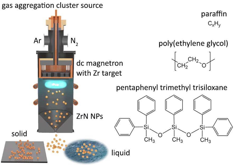 | ||
| Fig. 1 Scheme of dc magnetron-based gas aggregation cluster source used for the synthesis of ZrN NPs and their loading into vacuum-compatible liquids namely paraffin, PEG, and PTT. | ||
NPs produced in the GAS were extracted by the gas flow to the deposition chamber, where they were collected on Si substrates and TEM grids (Lacey Carbon Coated Gold Mesh, SPI Supplies). The distance between the substrate-holder and the orifice was 30 cm. The setup was also equipped with a mobile quartz crystal microbalance (QCM) system that was used to measure the deposition rate of NPs.
For the preparation of nanofluids, a Petri dish (5 cm in diameter) loaded with a host liquid was introduced to the deposition chamber through a load lock, which was pre-pumped by a rotary pump. Poly(ethylene glycol) (PEG, Mn = 400 g mol−1, Sigma-Aldrich, CAS-no: 25322-68-3), pentaphenyl trimethyl trisiloxane (PTT, Kurt J. Lesker, CAS-no: 3390-61-2) and liquid paraffin (Sigma-Aldrich, CAS-no: 8042-47-5) were used as vacuum-compatible host liquids. No stirring was applied during the deposition. After deposition, the as-deposited nanofluids were subjected to ultrasonication for 15 minutes.
Sample characterization
Scanning Electron Microscopy (SEM, JSM-7200F, Jeol Ltd) was used to calculate the flux of the NPs from the images obtained on sub-monolayers deposited on Si substrates. The measurements were made at 20 kV acceleration voltage and 3 × 10⁻¹⁰ A probe current.The structure of NPs was studied using a scanning transmission electron microscope (STEM, 2200FS, Jeol Ltd, Japan) with a FEG cathode operated at 200 kV acceleration voltage. The STEM was equipped with a Centurio Large Angle SDD-EDX detector. To investigate the elemental composition, bright-field (BF) STEM in combination with energy dispersive analysis (STEM-EDS) was used.
The chemical composition of the NPs deposited on Si was characterized using an X-ray photoelectron spectrometer (XPS, Phoibos 100, Specs) equipped with an Al Kα X-ray source (1486.6 eV, 200 W, Specs). The XPS analysis chamber was connected to the deposition chamber via a high-vacuum transfer, so it was possible to analyze the samples immediately after preparation without exposing them to ambient air. After the measurements, the same samples were extracted to air and analyzed again after one-day storage for comparison. The XPS spectra were acquired at a constant take-off angle of 90°. Wide spectra were obtained at a pass energy of 40 eV (dwell time 100 ms, step 0.5 eV). The high-resolution spectra were recorded at a pass energy of 10 eV (dwell time of 100 ms, step size of 0.05 eV, with 10 repetitions). In both cases, the spectra were analyzed using the CasaXPS software (v. 2.3.19PR1.0, Casa Software Ltd) with the charge reference to the adventitious C 1s peak at 285.0 eV. The best fits were obtained using Gaussian–Lorentzian (70/30) line shapes.
The size distributions of NPs deposited on silicon wafers were examined statistically by small-angle X-ray scattering (SAXS). The measurements were made on a laboratory instrument Xenocs SAXS Xeuss 2.0 with a Mo X-ray tube (Mo Kα radiation with λ = 0.07107 nm) using a hybrid pixel array detector Dectris Pilatus 200k. The distance between the sample and detector was set at 2500 mm. The raw data were subjected to azimuthal integration, background correction and normalization, and the resultant 1D SAXS curves were fitted in the IRENA45 and SASview46 programs to obtain the NP size distribution. The form factor of spherical core@shell NPs was used to fit the data for Zr NPs, whereas the form factor of cube core@shell NPs was used to fit the data for ZrN NPs. In both cases, models of diluted spheres and cubes were used, and lognormal size distribution was assumed.
The crystal structure was determined by X-ray diffraction (XRD) measurements performed on a Rigaku SmartLab diffractometer with a rotating copper anode (CuKα radiation λ = 0.15418 nm) in the parallel beam geometry. The data analysis was done using the program MStruct.47
The electrical conductivity of individual ZrN NPs was measured in air by conductive AFM using a highly conductive single diamond tip (TipsNano, DEP01, boron-doped diamond, macroscopic resistivity is 0.003–0.005 ohm m, tip radius is 7 nm). A sub-monolayer of ZrN NPs was deposited on 100 nm Au-covered silicon, and the Au film was grounded for the measurements. First, the sample was scanned in an intermittent contact mode to identify the area of interest. The device was then switched to a contact mode, the tip was brought into contact with a specific site on the sample surface and current–voltage (I–V) characteristics were recorded by applying a voltage bias of −1.0 V to +1.0 V between the tip and the Au film. The sites of interest included the Au surface and individual ZrN NPs. For each site, 100 I–V curves were obtained and averaged. All measurements were performed with the same tip and at the same contact force. After the I–V measurements, the area of interest was scanned again in the intermittent contact mode to make sure that the topography of the surface and the tip shape did not change. More details can be found in Fig. S1 of the ESI.†
The optical properties of nanofluids were studied by UV-Vis spectroscopy (Hitachi U-2900). The spectra were recorded in the range of 325–1100 nm using PMMA cuvettes filled with nanofluid and host liquid as a reference.
The chemical structure of the host liquids was characterized by liquid-state 1H nuclear magnetic resonance spectroscopy (NMR Bruker Avance 500, operated at 500.1 MHz). Prior to measurements, the liquids were dissolved in deuterated solvents for better spectral resolution (PEG in chloroform; paraffin and PTT in acetone, respectively).
Steady-state and time-resolved PL spectra were measured on the blank solvent and on the sample with NPs. The steady-state spectra were excited with a 325 nm laser of 3.8 × 10⁻⁵ J cm−2 s−1 power density, and the PL was collected via an optical fiber coupled to a spectrograph with a CCD camera. The time-resolved PL was obtained by exciting the sample with 200 fs pulses generated by the solid-state laser (Pharos) at a 1 kHz repetition rate. The fundamental wavelength of 1030 nm was converted to 355 nm using OPA. The peak power density was 3.2 × 10⁷ J cm−2 s−1. The PL was collected using achromatic doublets and sent onto the spectrograph coupled with a Hamamatsu streak camera (time resolution of 30 ps). The presented PL spectra are corrected for the spectral response of the detection system.
DFT calculations
The theoretical calculations were performed at the spin-polarized density functional theory (DFT) level using the Vienna Ab initio Simulation Package (VASP v.6.2.1).48,49 The electron-ion interaction was described using the projector augmented wave (PAW) method while electronic exchange and correlation effects were treated under the generalized gradient approximation (GGA) with the Perdew–Burke–Ernzerhof (PBE) functional.50 The plane-wave cutoff energy was set at 500 eV with a Monkhorst–Pack k-point grid of 3 × 3 × 3 (bulk) or 3 × 3 × 1 (ZrN/organic interface). For interface calculations, the DFT-D3 semi-empirical Grimme method was used to account for the van der Waals interactions between the organic molecules and the ZrN surface.51 For bulk calculations, the lattice vectors and atomic positions were fully relaxed using the conjugated gradient algorithm with the criteria of 10−5 eV for energy and 0.02 eV Å−1 for the atomic forces. For organic molecules deposited on ZrN, the lattice vectors were frozen to their bulk value. The molecule was relaxed on the surface using similar criteria on energy and forces.Oxygen-doped ZrN structures were modeled from the 2 × 2 × 2 supercell (Zr32N32) of the conventional ZrN fcc bulk. Randomized substitutions of zirconium and nitrogen atoms by oxygen atoms were done on this supercell to generate three doped structures of atomic composition Zr32N28O4, Zr30N23O11 and Zr22N15O27. All these structures were fully relaxed prior to the computation of their electronic density of states and band structures.
For the interface calculations, a vacuum region was set along the c direction of the previous ZrN supercell to generate a (100) ZrN surface with a thickness of 4 layers. A simplified version of the molecules used in the experiment was deposited on top of the surface. PEG was approximated with ethylene glycol OH–CH2–CH2–OH, paraffin with propane C3H8, and PTT with methyl(phenyl)silanediol C6H5–Si(CH3)–(OH)2.
The interaction (adsorption) energy Eads between organic molecules and the ZrN (100) surface was calculated using eqn (1):
| Eads = EZrN/mol − EZrN − Emol | (1) |
Here, EZrN/mol is the total energy of the interface comprising an organic molecule in contact with ZrN, while EZrN and Emol are the energies of the bare ZrN surface and free molecule in their interface geometry. Atomic charges and magnitude of the bonds formed at the surface were computed from the electronic density using the DDEC/6 scheme.52,53
To take into account possible surface oxidation of ZrN, we performed additional calculations of molecular interactions using the same unit cell but with 50% substitution of N with O, thus generating the surface of Zr2NO.
FDTD calculations
Finite-Difference Time-Domain (FDTD) simulations were performed using the Lumerical FDTD (Ansys, Inc.) software package to evaluate the optical properties of ZrN NPs dependent on their shape, oxidation, and solvent dielectric function. Perfectly matching layer boundaries were used to truncate a cubic simulation domain with a side of 100 nm filled with a homogeneous medium. A single NP was placed in the center of this domain and irradiated with a Total-Field Scatter-Field (TFSF) broadband source with wavelengths in the range of 300–1000 nm. Spherical ZrN NPs with a diameter of 22 nm, cubic ZrN NPs with an edge length of 22 nm, and cubic ZrN/ZrO2 core/shell NPs with a core of 18 nm and a shell of 2 nm were considered. The dielectric constants were taken from the literature for ZrN,54 PEG,55 paraffin,56 polydimethylsiloxane (PDMS),57 and benzene.58 The dielectric constants for ZrO2 were determined by performing spectroscopic ellipsometry measurements (ellipsometer M-2000, Woolam) on sputtered Zr coatings annealed in air at 800 °C for 4 hours. Absorption and scattering were analyzed by the advanced analysis group monitors positioned within the total-field and scatter-field regions of the TFSF source.Results and discussion
A preliminary series of experiments was performed using Ar without N2 to investigate how the deposition rate of metal Zr NPs and the bias on the magnetron are influenced by the gas flow (Fig. 2a and b). The Ar flow was increased stepwise with a time step of 30 s and the QCM and bias values were recorded at the end of each interval. The deposition rate was found to pass through a maximum, whereas the magnetron bias decreased monotonically. The trend corresponds to that of earlier studies on sputtered thin films, showing that a low ionization efficiency at a low pressure and a collisional sheath at a high pressure are the main factors that influence the efficiency of sputtering.59 The experiment allowed us to choose 11.0 sccm per 50 Pa of Ar as the conditions of the maximum deposition rate of Zr NPs.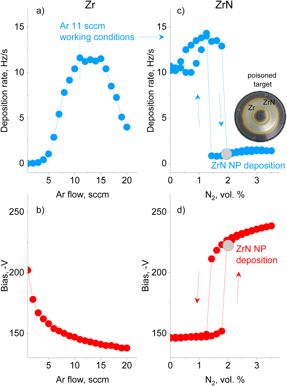 | ||
| Fig. 2 The deposition rate of NPs and dc bias at the magnetron for: (a and b) sputtering of Zr in Ar under different flow rates; (c and d) sputtering of Zr in Ar/N2 (the Ar flow rate is fixed at 11.0 sccm and the N2 flow rate is increased stepwise). The magnetron current is fixed at 500 mA. The gray symbols designate the working conditions for the synthesis of ZrN NPs. The inset shows the top view of the Zr target after many runs of reactive sputtering. | ||
In the following series, reactive magnetron sputtering in Ar/N2 was investigated to produce ZrN NPs (Fig. 2c and d). The experiment started in Ar at a flow rate of 11.0 sccm, and then N2 was sequentially added with a 0.02 sccm step every 30 s. In the early stage, the deposition rate and bias remain constant or increase slightly until the concentration of N2 reaches 1.8 vol%. At this point, continual nitridation leads to the target poisoning, which is represented by a sudden decrease in the deposition rate and an increase in the bias. A further increase in the N2 concentration results in an increase in the bias, but has a minor effect on the deposition rate, which remains almost constant. Note that the total pressure in the GAS does not exceed 50.5 Pa under the highest concentration of N2 reached, which allows us to consider the pressure to be roughly constant. If the flow of N2 is decreased, the deposition rate and the bias follow the hysteresis curves, with the onset of the metallic mode occurring at the lower N2 concentration of 1.4 vol%. Thus, reactive magnetron sputtering of Zr in the GAS configuration obeys the same phenomenology as observed in thin-film deposition.60 It should be noted that the onset of poisoning changes slightly with the utilization of the target. Therefore, in the following experiments, the same procedure of starting in Ar, adding N2 and reaching poisoning was used, and the nitrogen content immediately after reaching poisoning was chosen as the working condition for the deposition of ZrN NPs. Interestingly, the photo of the Zr target taken after numerous experimental runs (inset in Fig. 2) shows the characteristic golden color at the exterior and interior of the erosion track, pointing to the formation of ZrN in these areas. However, the erosion track itself retains a metallic luster, evidencing that sputtering was performed under weak poisoning.
The SEM and TEM measurements were performed to confirm that NPs were produced under the chosen conditions. Fig. 3 shows the results of such measurements on samples prepared in Ar (Zr NPs) or Ar/N2 (ZrN NPs) and deposited on Si substrates and TEM grids. Zr NPs appear spherical under a lower magnification of SEM (Fig. 3a); however, at closer TEM investigation, they reveal a multifaceted shape of the polyhedral morphology (Fig. 3b and c). The Zr NPs exhibit a distinct hexagonal shape in the orthogonal projection, which agrees with the high degree of crystallinity of Zr (see also the XRD results below). The ZrN NPs produced by reactive magnetron sputtering are dominated by cubic morphology, evidencing that the incorporation of nitrogen atoms changes the crystallinity (Fig. 3d–f). Although there exists an extensive literature on the synthesis of ZrN NPs by various methods,10,28,29 we note that reports on ZrN NPs with a well-defined cubic shape are rare.26 For gas-aggregated metal NPs, the formation of a cubic or spherical shape is governed by an interplay between the rate of arrival of metal atoms on the surface of a growing particle and the surface diffusion.61 Both parameters dynamically change as the NPs thermalize from the close-to-melting point temperature near the magnetron to the ambient temperature at farther distances via collisions with Ar atoms. In the case of reactive sputtering, a high metal-to-nitrogen bond enthalpy provides an additional channel for the energy gain by the NPs, and it can be assumed that the thermalization of NPs proceeds slower, providing close-to-equilibrium conditions for atomic rearrangements and crystallization. As a result, cubic NPs are preferentially formed, with the shape replicating the equilibrium fcc lattice structure of ZrN.
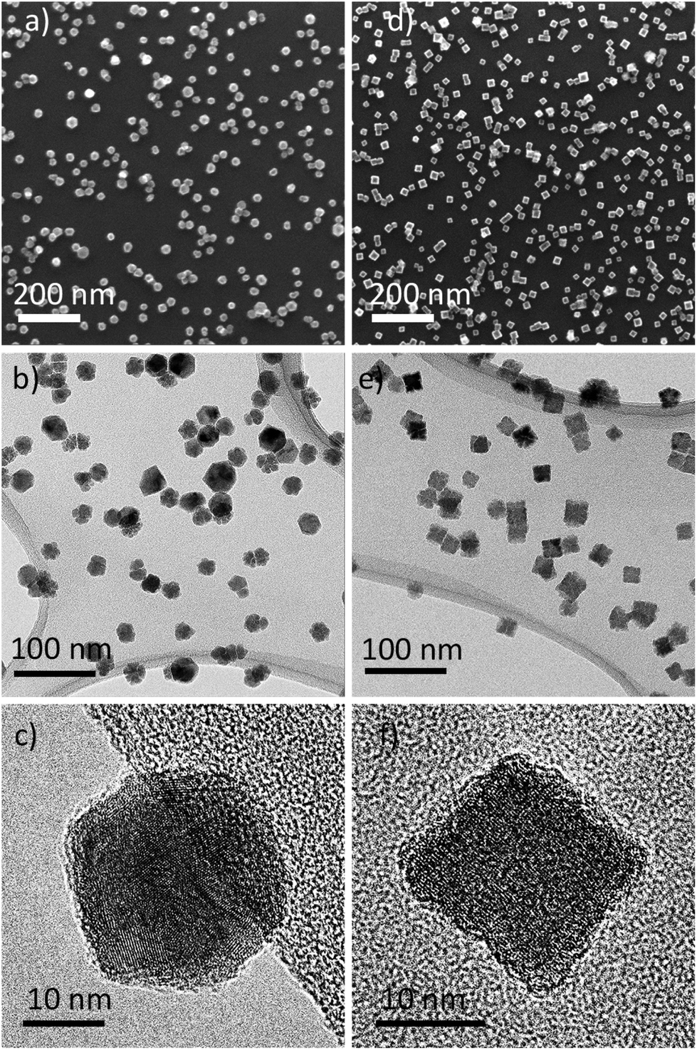 | ||
| Fig. 3 Morphology of Zr NPs (left column) and ZrN NPs (right column) investigated by SEM (a and d) and TEM (b, c, e and f). | ||
The structural and chemical peculiarities of these NPs were further investigated using STEM-EDS (Fig. 4). The results support the earlier drawn conclusion that Zr NPs are characterized by hexagonal projections, whereas ZrN NPs are of cubic shape. However, the most significant observations emerge from the data of elemental mapping. Zr NPs exhibit a core@shell structure consisting of a Zr core and an oxide shell. Most probably, the oxide appears because of the post-deposition oxidation, since the samples were analyzed after being exposed to the ambient atmosphere. Scanning across the NP projection reveals that the thickness of the ZrO2 shell is approximately 2 nm.
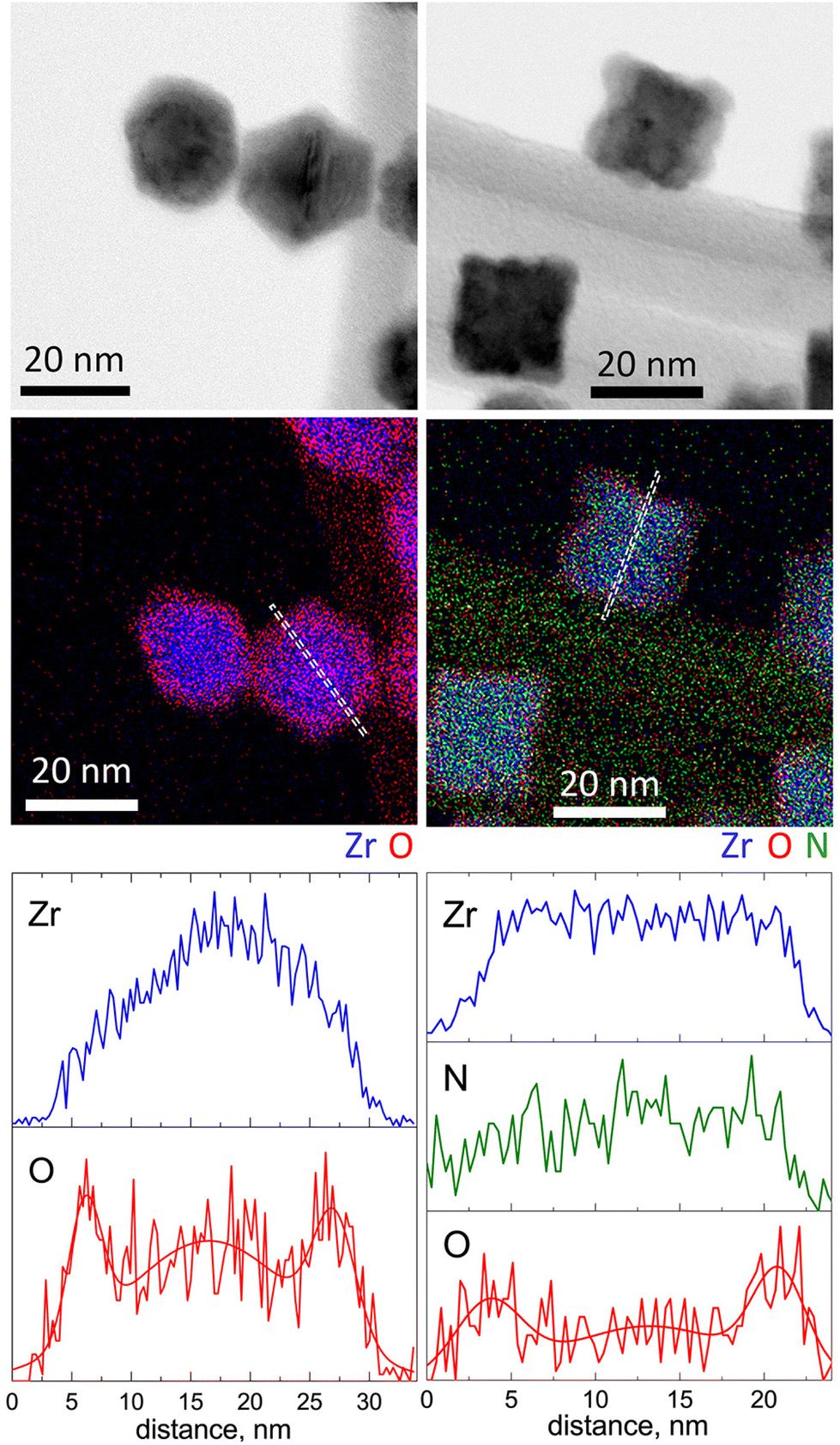 | ||
| Fig. 4 STEM-EDS analysis of Zr (left column) and ZrN (right column) NPs: BF STEM, elemental maps and scans along the profile lines. | ||
Importantly, in ZrN NPs, Zr and N are found to be homogeneously mixed within the entire volume, whereas the outermost regions are enriched with oxygen, although to a lesser extent than in Zr NPs. As determined from the elemental profile line, the thickness of the oxynitride layer is also approximately 2 nm.
X-ray scattering methods were applied to study the size distribution and crystallinity of the NPs in more detail. Fig. 5a–d shows the SAXS curves, the fits to these curves, and the resultant size distributions of Zr and ZrN NPs. Given the STEM-EDS data, the scattering curves were fitted using models of diluted spheres and cubes for Zr and ZrN NPs, respectively. In the case of Zr NPs, the spheres are approximations of polyhedral NPs. In both cases, lognormal size distribution was chosen which corresponds to typical size distributions of gas-aggregated NPs.44 Zr NPs are characterized by the mean size (diameter) of 21 ± 2 nm. ZrN NPs have the mean size (cube edge length) of 22 ± 3 nm. For comparison, the size distributions were also calculated from the SEM images and results are shown in Fig. S2 of the ESI.† Taken together, the STEM-EDS and SAXS results suggest that Zr and ZrN NPs are prone to partial oxidation when exposed to air. The oxidation leads to the formation of the ZrO2 and ZrNO layers that will presumably protect the inner core from further oxidation.
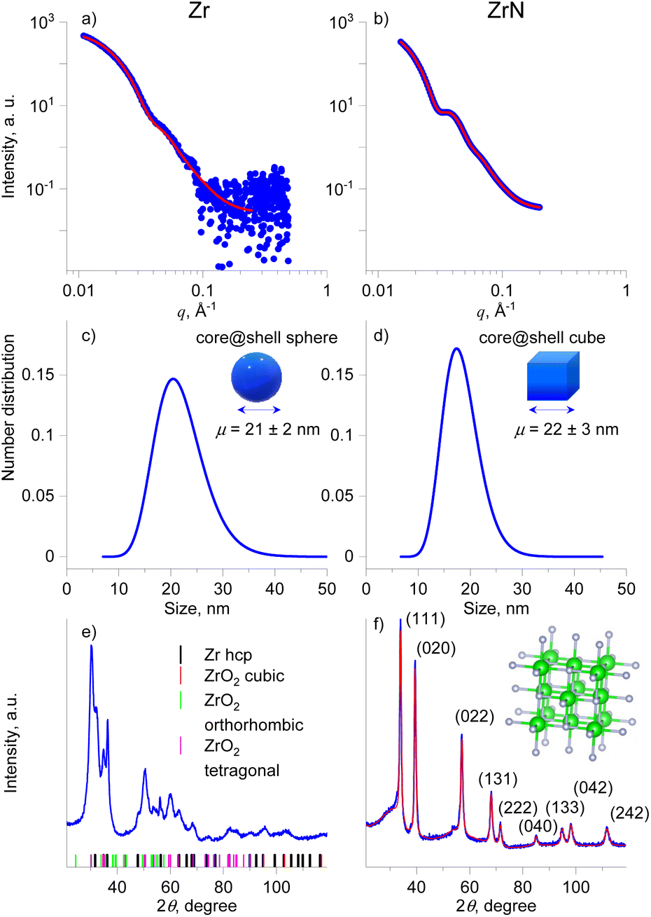 | ||
| Fig. 5 Size and crystallinity investigations of Zr NPs (left column) and ZrN NPs (right column): (a and b) SAXS data with fitting curves; (c and d) size distribution obtained from SAXS fitting using a spherical model for Zr and cubic model for ZrN; (e and f) XRD patterns. Red curves in a, b, f are fits to the experimental data. | ||
The XRD patterns acquired on multilayers of Zr and ZrN NPs deposited on Si wafers are shown in Fig. 5e and f. For Zr NPs, the XRD pattern contains peaks arising from multiple phases. The positions of the most probable phases are shown by colored dashes below the pattern. The most reliably identified are the hcp structure of Zr (space group 194) and the tetragonal crystalline phase of ZrO2 (space group 137); however, other ZrO2 polymorphs, including cubic and orthorhombic, cannot be ruled out due to the strong overlap of the broad peaks. This broadness points to the nanosize of the crystallites.
The addition of nitrogen completely changes the XRD pattern, which becomes better resolved, with positions of individual peaks matching the pattern of the fcc phase of ZrN and space group 225 (the unit cell is shown in the inset of Fig. 5f). In this case, the XRD pattern allows for reliable fitting (Table 1), yielding the lattice parameter of 4.5630 Å, the mean crystallite size of 14 nm, and a microstrain of 0.46%, which describes the relative deviation in the lattice parameter within the crystal. We note that the mean crystallite size is close but slightly smaller than the NP mean size of 22 nm (18 nm core) inferred from the SAXS analysis. Such proximity of values is worth highlighting, as it points to the fact that ZrN NPs are formed by single crystallites that constitute the NP core, with a minor contribution from the amorphous phase that is present in the form of the oxynitride shell. Another striking observation to emerge from the analysis is that highly crystalline ZrN NPs were obtained without heating substrates. For thin films, annealing is often considered necessary to provide the activation energy for surface and volume atomic diffusion. Thermally activated atomic rearrangements lead to crystalline ZrN films of high quality.12,14,62 Gas-phase aggregation of NPs with or without equilibrium shapes has often been considered through the prism of their cooling from the quasi-liquid state driven by the kinetics of energy gains and losses.63,64 Our findings indicate that the growth and transport of ZrN NPs proceed under the energetic conditions that provide sufficiently slow cooling to facilitate the atomic rearrangement toward the fcc structure and the formation of cubic nanocrystals.
| Fitted parameters | ZrN cubic phase |
|---|---|
| Lattice parameter, Å | 4.5630 (3) |
| Mean size of crystallites, nm | 14 ± 1 |
| Microstrain, % | 0.46 ± 0.05 |
The above results are further supported by the XPS analysis that was performed on Zr and ZrN NPs immediately after their preparation without breaking the vacuum and after one day of storage in air (Fig. 6). Zr 3d XPS spectra are deconvoluted using pairs of spin–orbit split 3d5/2 and 3d3/2 components, separated from each other by a fixed theoretical value of 2.4 eV and with an area ratio fixed at a theoretical value of 3/2. The XPS spectrum of Zr NPs is dominated by the doublet with the most intensive 3d5/2 component positioned at 178.1 eV and corresponding to metal Zr. A higher binding energy tail evidences that partial oxidation still occurs due to residual oxygen in the deposition chamber. Hence, the peaks belonging to ZrO2 are added to the fit, with the most intensive 3d5/2 component positioned at 181.8 eV. Furthermore, Zr suboxides should be added between Zr and ZrO2 to achieve a satisfactory fit. The analysis of the elemental composition gives the ratio of O/Zr = 0.5.
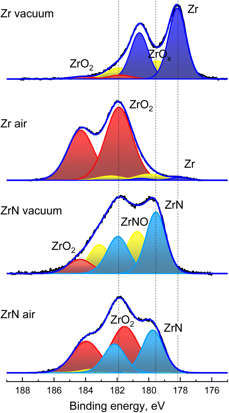 | ||
| Fig. 6 XPS Zr 3d spectra of Zr and ZrN NPs acquired immediately after sample preparation without breaking vacuum and after one day storage in air. | ||
For the same sample aged in air, the dominant peaks in the 3d spectrum are those belonging to ZrO2, whereas the signal from the metal Zr core becomes strongly attenuated. The chemical picture corresponds to the formation of the oxide shell around Zr NPs. Analysis of the elemental content shows that the O/Zr ratio changes to 1.9, which is also consistent with the presence of the ZrO2 shell.
The XPS spectra of ZrN NPs look different: for the sample measured without breaking vacuum, the spectrum lacks metal Zr, while the strongest 3d5/2 component is positioned at 179.5 eV between Zr and ZrO2. Given the XRD results, we attribute it to ZrN. The assignment is further supported by the elemental content, which gives the ratio of N/Zr = 1.0. The ZrN NPs are also partially oxidized, as is evident from the presence of minor ZrO2 peaks. For consistency, an additional doublet was added between the ZrO2 and ZrN components, which can be generically assigned to ZrNO.
The oxidation of ZrN NPs becomes more prominent after aging for one day. The lower binding energy part of the spectrum is still enriched with the signal from ZrN, although the ZrO2 doublet becomes dominant. The analysis of the elemental content gives N/Zr = 0.7 and the overall formula is ZrN0.7O1.3. Since the XRD results unambiguously show the presence of the ZrN core in the oxidized NPs, the formula predominantly represents the chemical composition of the oxynitride shell.
Most studies on group IV MeN thin films have reasonably neglected the surface oxidation, as a nanometer-scale oxynitride layer may not be crucial for the performance of sub-micrometer-scale coatings; however, oxidation may become a serious factor for nanomaterials. We performed DFT calculations to investigate the influence of the oxynitride layer on the band structure and density of states (DoS) of ZrN (Fig. 7). Consistent with the earlier studies on stoichiometric ZrN, our results confirm the metallic character of Zr32N32, showing that the conduction and valence bands are formed predominantly by Zr-d and N-p orbitals, respectively, and that the Fermi level EF lies in the conduction band. The interband transitions occur at >2.6 eV, which is also consistent with the reported values.65 Several calculations were also made with the random substitution of N atoms by O atoms to simulate the partial oxidation of ZrN. Mild oxidation introduces the contribution from the O-p states, mainly in the valence band, although the overall shape of the DoS stays almost unchanged, evidencing that slightly oxidized Zr32N28O4 and Zr30N23O11 remain metallic. In the ultimate case of Zr22N15O27, which closely resembles the real oxynitride shell on the synthesized ZrN NPs with the XPS formula of ZrN0.7O1.3, a band gap of 2.2 eV appears while the EF is shifted toward the ceiling of the valence band, pointing to a p-type semiconductor characteristic of this material. Interestingly, a mid-gap state appears at about 1.2 eV, which we attribute to the formation of Zr–O–N–O–Zr functionalities accompanied by the hybridization between the N-p and O-p orbitals (for details, see Fig. S3, Fig. S4 and Table S1 of the ESI†). Thus, the electronic architecture of the ZrN/ZrNO interface might be roughly viewed as a metal–semiconductor junction, if an extremely small thickness of ZrNO is disregarded.
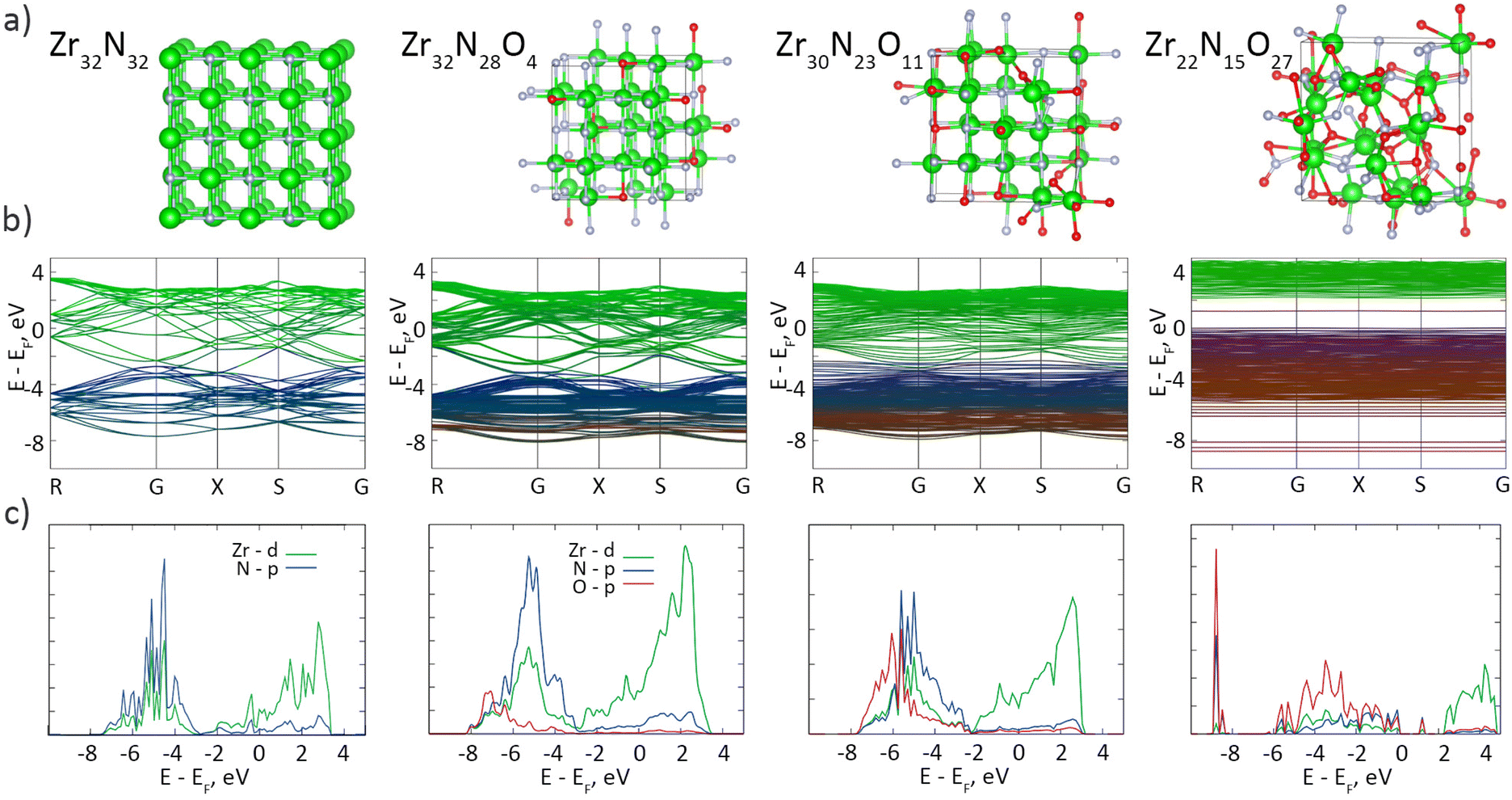 | ||
| Fig. 7 DFT calculations: (a) crystal cells; (b) band structures; (c) DoS of ZrN crystals (64 atoms in total) with different extents of oxygen substitutions. | ||
Conductive AFM was used to investigate the electrical properties of ZrN NPs deposited in sub-monolayers on gold-covered Si. First, an area of interest was identified in the intermittent contact mode (Fig. 8a), then the tip was brought into contact with individual NPs, and I–V curves were acquired. For comparison, the I–V curves were also measured on Au at the spots in between the NPs. ZrN NPs are found to be conductive, although they pass a smaller current compared to Au, obviously because of a smaller charge carrier density (Fig. 8b). In both cases, the I–V curves demonstrate a non-rectifying behavior, showing symmetric positive and negative branches with the same values of current reached at positive and negative polarities. It is also interesting that the shapes of the I–V curves look different for Au and ZrN: Au demonstrates the saturation at a high bias, whereas ZrN shows an increase of the current. The difference is seen even more clearly if the first derivative of voltage with respect to current is taken, showing that the differential resistance of ZrN becomes lower than that of Au at the voltage larger than ±0.5 V. A conductive tip in contact with an oxidized ZrN NP lying on a conductive substrate can be represented as a series of back-to-back Schottky junctions (top and bottom ZrNO layers) separated by a series resistance (ZrN bulk), and the appearance of Schottky barriers can be expected. Nevertheless, symmetric I–V curves evidence that the barriers are equal at both contact points. Furthermore, non-saturating character of the I–V curves points to a decrease of the barrier height with the applied voltage due to an image-force barrier lowering, an effect often observed in metal–semiconductor devices.66,67
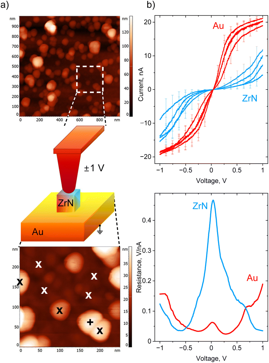 | ||
| Fig. 8 (a) Different scan size AFM images of ZrN NPs on Au with a scheme of the I–V measurements, “x” designates the spots used for obtaining the I–V curves; (b) site-selective I–V curves measured by a conductive tip on “x” spots and the averaged resistance (dV/dI). | ||
ZrN NPs deposited on solid supports can be easily transferred to liquids by ultrasonication, as shown in Fig. S5 of the ESI.† Motivated by our recent results on direct loading of sputtered Cu and Ag NPs in liquids,68,69 we also performed depositions of Zr and ZrN NPs in three vacuum-compatible liquids of different chemical compositions: PEG (polyether), paraffin (mixture of aliphatic hydrocarbons), and PTT (aromatic siloxane). The three types of nanofluids were prepared with the concentration of 50 μg ml−1 for Zr and 30 μg ml−1 for ZrN NPs. In addition to practical features, these nanofluids may also represent a scientific interest because they consist only of host liquids and NPs without any surfactant or additional chemicals, a benefit rarely achieved in wet chemical synthesis.
The liquids appear brownish in the case of Zr and bluish for ZrN, as demonstrated in Fig. 9a and b by exemplar photos of vials with Zr/paraffin and ZrN/paraffin nanofluids. It is worth noting that, similarly to metal nanofluids,70 ZrN nanofluids can be used as precursors for dilution with other solvents, provided that these are miscible with the host liquids. For example, PEG is very well miscible with water, and arbitrarily diluted ZrN/PEG/H2O solutions can be easily prepared by ultrasonication (Fig. S5 of the ESI†).
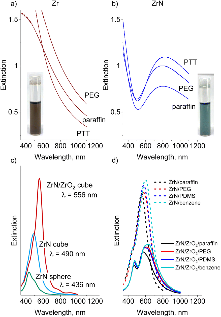 | ||
| Fig. 9 Measured UV-Vis spectra of (a) Zr (50 μg ml−1) and (b) ZrN (30 μg ml−1) nanofluids in PEG, paraffin and PTT (insets show vials with Zr/paraffin and ZrN/paraffin nanofluids). FDTD simulated extinction spectra of a single NP: (c) ZrN sphere (22 nm diameter) vs. ZrN cube (22 nm edge length) vs. ZrN/ZrO2 core@shell cube (18 nm core and 2 nm shell); (d) ZrN and ZrN/ZrO2 core@shell cube NPs in different liquids. | ||
The obtained UV-Vis spectra show that the Zr nanofluids absorb light in the blue region but exhibit a monotonically decreasing extinction in the red/near-IR region (Fig. 9a, for comparison, we also provide UV-vis spectra of Zr and ZrN NPs deposited on quartz substrates as shown in Fig. S6 in the ESI†). Nitridation of NPs noticeably influences the optical properties of the nanofluids: only a narrow transmittance window exists around 500 nm. Strong absorbance at λ < 500 nm correlates with the onset of p → d interband transitions in ZrN that occur at >2.6 eV (<477 nm), and another wide absorption band spreads from the red to the near-IR region (Fig. 9b). For the IV-group transition metal nitrides, enhanced absorption in this region is attributed to localized surface plasmon resonance, which is located at >500 nm for pure ZrN, red shifting with the incorporation of oxygen.24
To evaluate the influence of the NP shape/oxidation and solvent dielectric function on the optical extinction we performed FDTD simulations. Fig. 9c shows the spectra calculated for a single 22 nm-sized NP placed in vacuum and compares the spherical ZrN, the cubic ZrN, and the cubic ZrN/ZrO2 core/shell morphology. The position of the extinction maximum red shifts from λ = 436 nm for the spherical NP to λ = 490 nm for the cubic NP, and further to λ = 556 nm for the oxidized cubic ZrN/ZrO2 NP (note that the dielectric constants of the true zirconium oxynitride present on the surface are not known, and our model of ZrN/ZrO2 represents a rough approximation). The dielectric function of the host medium also plays a role in the red shift of the extinction spectra. Fig. 9d shows the spectra calculated for cubic ZrN NPs placed in different liquids. For PTT, the dielectric constants are not known, and we roughly approximated this medium by PDMS (siloxane bonds) and benzene (aromatics). ZrN NPs exhibit significant red shifts in extinction spectra when placed in the dielectric media, with larger shifts obtained for the oxygen-containing and aromatic media. Furthermore, the oxidized ZrN/ZrO2 NPs show even larger shifts, reaching λ = 635 nm for benzene. In this case, the calculations should be taken with care because they give bimodal spectra that are different from those measured. Most likely, the bimodal shape of the calculated spectra is the result of a sharp boundary between ZrN and ZrO2 introduced into the model, which does not reflect the existing oxidation gradient in real NPs. Our results are consistent with those reported earlier.71–73 Nevertheless, the measured positions of the extinction maxima are still very far from the calculated values, which points to the influence of other aspects not included in the model. For example, near-field interactions between closely positioned NPs are known to induce electromagnetic coupling, resulting in the red shift of LSPR by hundreds of nanometers.74
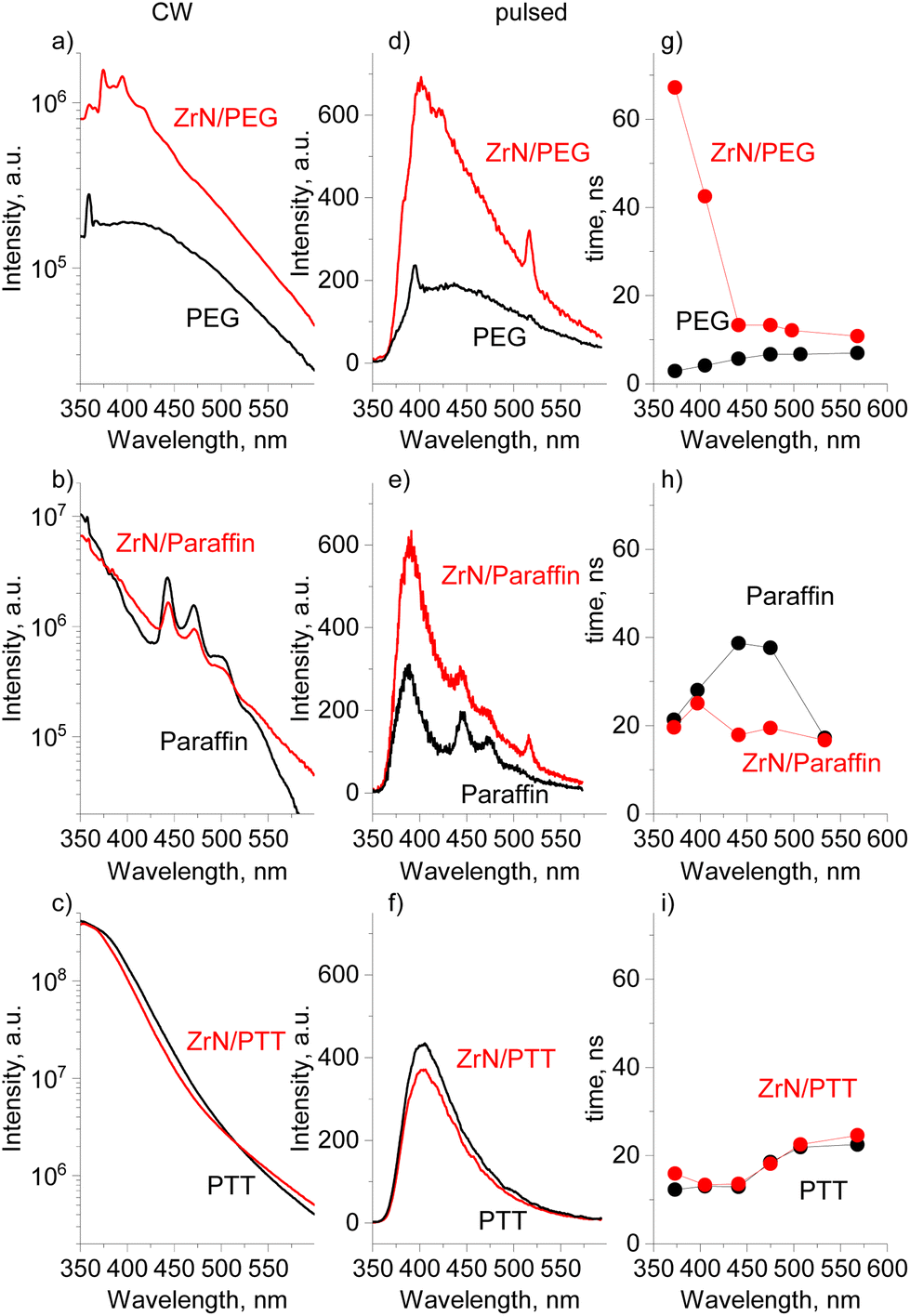
In anticipation of more complex optoelectronic phenomena, we have performed PL measurements using the continuous-wave (CW) and pulsed excitation on ZrN NPs deposited on Si in the dry state, the same ZrN NPs loaded in the liquids, and on the blank liquids without NPs. It should be noted that dry ZrN NPs on Si show no detectable PL signal regardless of the excitation laser.
In the steady-state PL measurements, all three blank solvents show PL emission (Fig. 10a–c), which is broad, spanning from 325 to 600 nm and maximizing in the near-UV/blue range. The integral PL intensity of the spectra increases in a sequence of PEG < paraffin < PTT. While for aromatic-based PTT, the PL is more than expected, PEG and paraffin do not contain either aromatics or conjugated features (Fig. S7–S9 of the ESI†) and hence they were often considered non-emissive in the past.75 The paradigm has recently changed as numerous π-conjugation-free organic molecules or polymers have been identified as being emissive, especially in concentrated solutions or in the solid state, and they have been classified as non-conventional luminophores.76 The photoluminescence of PEG is reportedly given by a cluster-triggered emission (CTE) mechanism: PEG molecules rearrange to acquire conformations in which oxygen atoms form clusters with through-space conjugation of their lone pairs, providing intrinsic chromophores.75,77 The PL of paraffin is quite a puzzle because intrinsic photoluminescence of nonconventional luminophores typically requires the availability of heteroatoms (such as O, N, etc.) and none is present in paraffin, a mixture of aliphatic hydrocarbons. Our complementary environmental XPS measurements taken directly on liquid paraffin under vacuum revealed no other elements except carbon (Fig. S7a of the ESI†). NMR 1H spectra showed the dominant contribution from the aliphatic CH2 and CH3 species (Fig. S7b of the ESI†), and the only possible reason for PL can be found in a tiny signal just above the background that could be attributed to the presence of alkenes. It remains an open question whether such a trace amount of the C![[double bond, length as m-dash]](https://www.rsc.org/images/entities/char_e001.gif) C bonds can provide high intensity PL, or whether there are other unknown mechanisms involved.
C bonds can provide high intensity PL, or whether there are other unknown mechanisms involved.
 | ||
| Fig. 10 Photoluminescence of ZrN nanofluids vs. blank solvents: (a–c) PL spectra at CW excitation (λexc = 325 nm); (d–f) PL spectra at pulsed excitation (λexc = 355 nm, 200 fs pulse length, 400 nJ per pulse); (g–i) average PL decay times at different emission wavelengths. | ||
The addition of ZrN NPs to liquids does not influence the shape of the CW emission curves, but significantly enhances the PL intensity for ZrN/PEG. For paraffin and PTT, the spectra look similar for the nanofluid and the blank solvent.
Pulsed excitation shows more peculiarities. The PL intensity becomes enhanced both for ZrN/PEG and ZrN/paraffin, compared to that of the blank solvents, whereas ZrN/PTT does not show significant changes (Fig. 10d–f). The PL decay curves were extracted from the temporally resolved PL measurements and the average decay times τavg are shown in Fig. 10g–i (the individual decay components of the fits can be found in Table S2 of the ESI†). The average PL decay time of the ZrN/PEG is longer than that of blank PEG in the whole emission range, and the deviation is particularly notable in the near-UV/blue range (the region of the strongest emission), where more than an order of magnitude prolongation has been detected. ZrN/paraffin shows a different behavior, with decay times similar to that of blank paraffin in the region of the strongest PL and shorter decay times for the nanofluid in the visible range. Another situation is observed for the ZrN/PTT nanofluid, which shows decay times very similar to those of blank PTT in the entire wavelength range. Obviously, the influence of ZrN NPs on the PL of organic molecules is governed by their chemical structure.
DFT calculations were performed to investigate the interaction between ZrN and the host liquids. To simplify the problem, we approximated the organic molecules used in the experiments by smaller analogues: PEG was approximated with ethylene glycol OH–CH2–CH2–OH, paraffin with propane C3H8, and PTT with methyl(phenyl)silanediol C6H5–Si(CH3)–(OH)2. Fig. 11 shows the side and top views of these molecules in their relaxed state on the (100) surface of ZrN, while Table 2 summarizes the adsorption energy Eads, charge on the molecule, and total bond order obtained as a result of the calculations.
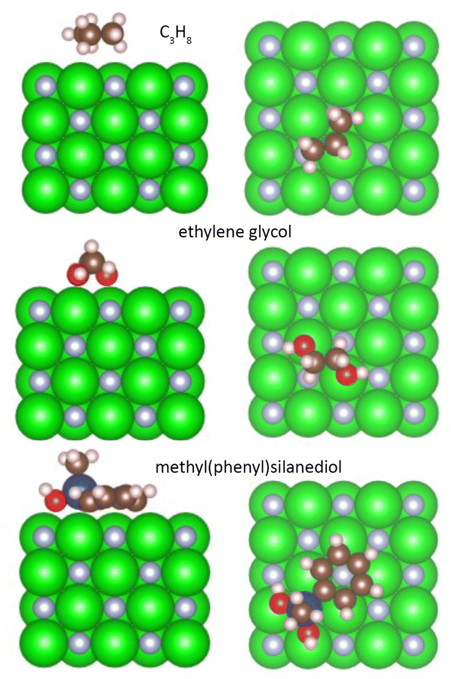 | ||
| Fig. 11 Relaxed interface geometries of propane, ethylene glycol, and methyl(phenyl)silanediol on the ZrN (100) surface. Left column is the side view, right column is the top view. | ||
| Parameter | C3H8 | OH–CH2–CH2–OH | C6H5–Si(CH3)–(OH)2 |
|---|---|---|---|
| E ads (ZrN) | −0.48 | −1.86 | −4.64 |
| E ads (Zr2NO) | −0.40 | −1.81 | −5.30 |
| Charge on molecule, e (ZrN) | −0.075 | −0.087 | −0.615 |
| Charge on molecule, e (Zr2NO) | −0.049 | −0.072 | −0.669 |
| Total bond order (ZrN) | 0.56 | 1.47 | 3.16 |
| Total bond order (Zr2NO) | 0.47 | 1.42 | 3.37 |
Aliphatic hydrocarbons promote the weakest interaction with ZrN, showing a total bond order of 0.56, Eads = −0.48 eV, and a small negative charge of −0.075 detected on the C3H8 molecule. In contrast, oxygen-containing molecules show a stronger interaction. Ethylene glycol interacts with ZrN primarily through the binding of hydroxyl oxygens to Zr atoms, which leads to a total bond order of 1.47 and Eads = −1.86 eV. Nevertheless, the charge transfer is not substantially larger compared to C3H8, with the charge on the ethylene glycol molecule reaching −0.087. The strongest interaction is found for methyl(phenyl)silanediol, which bears a phenyl ring and a siloxane linkage. Two oxygen atoms bind to Zr atoms on the surface, while the phenyl ring occupies an in-plane configuration and interacts with another Zr atom via the ortho-carbon. As a consequence, the total bond order increases to 3.16, Eads shows a large value of −4.64 eV, and the molecule bears a large negative charge of −0.615. The presence of the large charge on the analogue of PTT points to the formation of a strong dipole at the ZrN/molecular interface, whereas the dipoles in the case of paraffin and PEG are less prominent.
The same conclusions can be drawn if the oxidized Zr2NO surface is considered for molecular interactions. Relaxed interface geometries of the organic molecules on the Zr2NO (100) surface are shown in Fig. S4 of the ESI,† whereas the adsorption energy, charge on the molecule, and total bond order are given in Table 2. The addition of oxygen atoms to the surface enhances the difference in these parameters between the molecules in question. One can note, for example, that an even more negative charge of −0.669 is developed on methyl(phenyl)silanediol as compared to −0.072 for ethylene glycol and −0.049 for propane.
The noticeable result of the DFT calculations is that the charge on the organic molecules correlates in a specific way with the PL intensity in ZrN nanofluids. The large charge on PTT (strong interfacial dipole) is related to negligible changes in PL in both the CW and pulsed modes, whereas the small charge on PEG correlates with the enhancement of PL in both modes. For paraffin (with small molecular charge), the situation is controversial, as we do not observe significant changes in the CW mode, but we detect the PL enhancement under the pulsed excitation. This apparent discrepancy can be explained by a significant difference in the laser power density, which was 12 orders of magnitude higher in the case of the pulsed excitation. Thus, pulsed excitation produces much higher exciton populations compared to CW excitation, which was also observed in ref. 78.
Identical shapes and different intensities of the PL spectra of ZrN nanofluids and the blank solvents imply that the PL phenomena are related to the generation of hot carriers in ZrN due to the interband transitions, followed by relaxation, trapping, and escape of the carriers from ZrN to adjacent organic molecules. Thermalization of hot carriers in ZrN is non-radiative (no PL observed on dry NPs) but proceeds via electron–electron and electron–phonon scattering, the latter being the limiting factor with the hot carrier lifetime of 10 fs calculated in ref. 79 or about 1 ns measured on thin films in ref. 80. The mean free path of hot carriers in ZrN was calculated to be 10 nm (close to the Fermi level),79 which makes them accessible on the surface of our 22 nm sized NPs. For PEG and paraffin, a weak interfacial dipole does not introduce high energetic barriers to limit the transfer of energy from the NPs to the solvents. In contrast, the PL of ZrN/PTT is close to that of the blank PTT, pointing to a limited energy transfer because of a strong interfacial dipole.
It should be noted that enhanced PL from organic molecules has recently been reported for periodically arrayed ZrN thin films.81 The effect was attributed to LSPR-related phenomena, which were enhanced in the direction of the nanopattern plane. In our experiments, the concentration of ZrN NPs (30 μg ml−1) is sufficiently low to ensure that the mean distance between the NPs exceeds the size of the NPs by at least an order of magnitude. Considering also that the nanofluids were excited at λexc very distant from the position of the LSPR of ZrN, we find plasmonic coupling between the NPs highly unlikely. To conclude, we emphasize that our explanation of the observed PL effects is by far non-exhaustive, and more research should investigate the origin of the PL, including enhancement/quenching mechanisms.
Conclusions
ZrN NPs can be produced at the onset of the reactive mode of dc sputtering of the Zr target in a mixture of Ar and N2 under an elevated pressure of 50 Pa, without the use of aggressive chemicals and without additional annealing. NPs are characterized by a mean size of 22 ± 3 nm and have a cubic morphology, which is a derivative of their crystallinity: the XRD pattern perfectly matches the fcc phase (space group 225) of stoichiometric ZrN. The mean size of the crystalline domains is 14 nm, which indicates that NPs are formed by single crystallites with a minor contribution from the amorphous phase. The amorphous phase is present in the form of a 2 nm shell of oxynitride that appears as a result of post-deposition oxidation of NPs in air.The ZrN core has an electronic band structure corresponding to that of metals, whereas the oxynitride shell bears features of a semiconductor, with a bandgap of 2.2 eV and mid-gap states due to hybridization between the N and O p orbitals. Nevertheless, the oxynitride layer is too thin to interfere with the electric current flowing under the applied bias, and ZrN NPs are found to be electrically conductive.
Fluxes of ZrN NPs can be directed on the surface of vacuum-compatible liquids to produce nanofluids, in which the concentration of NPs is controlled by the deposition time. Three types of ZrN nanofluids were successfully prepared using three host liquids with different chemical compositions: polyethylene glycol (PEG), paraffin, and pentaphenyl trimethyl trisiloxane (PTT). The fluids are of bluish color, which is given by a broad LSPR positioned in the red/near-IR region and by strong absorption at λ < 500 nm due to interband transitions in ZrN. The nanofluids also demonstrate a complex photoluminescence (PL) behavior. ZrN NPs enhance the PL of PEG and paraffin, especially under more energetic pulsed excitation, whereas the PL of PTT remains almost invariable regardless of the excitation mode. DFT calculations revealed that changes in the PL correlate with the charge on organic molecules in contact with ZrN. For paraffin and PEG, the interaction with ZrN is weak, the molecular charge is small, and a low interfacial barrier for charge transfer results in the enhancement of the PL of the liquids. For strongly interacting PTT with the large charge on the molecule, the energetic barrier is too high and the PL is not affected. In summary, the results reported here provide the first evidence for highly crystalline, electrically conductive, and stoichiometric ZrN NPs produced by reactive dc sputtering and loaded into host liquids without extensive chemical pathways. On the basis of this approach, more complex nanofluids can be envisioned that may offer unique opportunities for fundamental and applied research.
Author contributions
Mariia Protsak – investigation, funding acquisition, methodology, validation, and writing; Kateryna Biliak – investigation and data curation; Daniil Nikitin – investigation and formal analysis; Pavel Pleskunov – investigation and software; Marco Tosca – investigation and validation; Suren Ali-Ogly – investigation and software; Jan Hanuš – investigation; Lenka Hanyková – investigation; Veronika Červenková – investigation and visualization; Anastasiya Sergievskaya – investigation; Stephanos Konstantinidis – investigation and resources; David Cornil – investigation, software, and writing; Jérôme Cornil – investigation, resources, and writing; Miroslav Cieslar – investigation; Tereza Košutová – investigation; Tomáš Popelář – investigation; Lukáš Ondič – investigation, resources, and writing; Andrei Choukourov – conceptualization, funding acquisition, investigation, project administration, resources, supervision, and writing.Conflicts of interest
There are no conflicts to declare.Acknowledgements
The work was supported by the Czech Science Foundation via the grant GACR 21-12828S. Mariia Protsak acknowledges the support from the Charles University via the student grant GAUK 372322. Students S. A.-O., K. B, and M. T. acknowledge the support from the Charles University via the grant SVV 260700-2023. The DFT calculations were supported by the Consortium des Équipements de Calcul Intensif (CÉCI), funded by the Fonds National de la Recherche Scientifique (F. R. S.-FNRS) under Grant No. 2.5020.11. J. C. and S. K. are FNRS research fellows. T. P. and L. O. acknowledge the support from the project Lumina Quaeruntur of the Czech Academy of Sciences. The authors thank Miquel Gamon Rodriguez for environmental XPS measurements.References
- U. Guler, G. V. Naik, A. Boltasseva, V. M. Shalaev and A. V. Kildishev, Appl. Phys. B: Lasers Opt., 2012, 107, 285–291 CrossRef CAS.
- G. V. Naik, V. M. Shalaev and A. Boltasseva, Adv. Mater., 2013, 25, 3264–3294 CrossRef CAS PubMed.
- U. Guler, A. V. Kildishev, A. Boltasseva and V. M. Shalaev, Faraday Discuss., 2015, 178, 71–86 RSC.
- A. Lalisse, G. Tessier, J. Plain and G. Baffou, Sci. Rep., 2016, 6, 1–10 CrossRef PubMed.
- S. Juneja and M. S. Shishodia, Opt. Commun., 2019, 433, 89–96 CrossRef CAS.
- P. Patsalas, Thin Solid Films, 2019, 688, 137438 CrossRef CAS.
- M. Dasog, Chem. Mater., 2022, 34, 4249–4258 CrossRef CAS.
- F. Yin, K. Takanabe, J. Kubota and K. Domen, J. Electrochem. Soc., 2010, 157, B240 CrossRef CAS.
- R. Chandiramouli and V. Nagarajan, Spectrochim. Acta, Part A, 2015, 136, 1018–1026 CrossRef CAS PubMed.
- Y. Yuan, J. Wang, S. Adimi, H. Shen, T. Thomas, R. Ma, J. P. Attfield and M. Yang, Nat. Mater., 2020, 19, 282–286 CrossRef CAS PubMed.
- A. Schlegel, P. Wachter, J. J. Nickl and H. Lingg, J. Phys. C: Solid State Phys., 1977, 10, 4889–4896 CrossRef CAS.
- S. A. Barnett, L. Hultman, J. E. Sundgren, F. Ronin and S. Rohde, Appl. Phys. Lett., 1988, 53, 400–402 CrossRef CAS.
- N. Farkas, G. Zhang, R. D. Ramsier, E. A. Evans and J. A. Dagata, J. Vac. Sci. Technol., A, 2008, 26, 297–301 CrossRef CAS.
- A. B. Mei, B. M. Howe, C. Zhang, M. Sardela, J. N. Eckstein, L. Hultman, A. Rockett, I. Petrov and J. E. Greene, J. Vac. Sci. Technol., A, 2013, 31, 061516 CrossRef.
- M. Gharib, M. J. Eshraghi and M. Bordbari, J. Mater. Sci.: Mater. Electron., 2020, 31, 21515–21527 CrossRef CAS.
- C. P. Mejía, H. S. Vanegas and J. J. Olaya, Coatings, 2022, 12, 754 CrossRef.
- M. S. El-Eskandarany and A. Ashour, J. Alloys Compd., 2000, 313, 224–234 CrossRef CAS.
- Y. Sun, B. Yao, Q. He, F. Su and H. Z. Wang, J. Alloys Compd., 2009, 479, 599–602 CrossRef CAS.
- Y. Gu, F. Guo, Y. Qian, H. Zheng and Z. Yang, Mater. Lett., 2003, 57, 1679–1682 CrossRef CAS.
- S. K. Lee, K. T. Park, H. Y. Ryu, H. H. Nersisyan, K. H. Lee and J. H. Lee, Korean J. Mater. Res., 2012, 22, 243–248 CAS.
- S. Zhao, J. Ma, R. Xu, X. Lin, X. Cheng, S. Hao, X. Zhao, C. Deng and B. Liu, Sci. Rep., 2019, 9, 1–9 CrossRef PubMed.
- O. A. Baturina, A. Epshteyn, A. C. Leff, A. P. Purdy, T. Brintlinger, B. S. Simpkins, E. Y. Santiago and A. O. Govorov, J. Electrochem. Soc., 2021, 168, 016503 CrossRef CAS.
- Y. Liu, X. Zhang, L. Lu, J. Ye, J. Wang, X. Li, X. Bai and W. Wang, Chin. Chem. Lett., 2022, 33, 1271–1274 CrossRef CAS.
- A. Reinholdt, R. Detemple, A. L. Stepanov, T. E. Weirich and U. Kreibig, Appl. Phys. B: Lasers Opt., 2003, 77, 681–686 CrossRef CAS.
- T. Avsievich, R. Zhu, A. P. Popov, A. Yatskovskiy, A. A. Popov, G. Tikhonowsky, A. I. Pastukhov, S. Klimentov, A. Bykov, A. Kabashin and I. Meglinski, Pharmaceutics, 2023, 15, 1046 CrossRef CAS PubMed.
- J. L. H. Chau and C. C. Kao, Mater. Lett., 2007, 61, 1583–1587 CrossRef CAS.
- D. Van Lam, H. Suematsu and T. Ogawa, J. Am. Ceram. Soc., 2017, 100, 4884–4892 CrossRef.
- S. Exarhos, A. Alvarez-Barragan, E. Aytan, A. A. Balandin and L. Mangolini, ACS Energy Lett., 2018, 3, 2349–2356 CrossRef CAS.
- R. A. Karaballi, G. Humagain, B. R. A. Fleischman and M. Dasog, Angew. Chemie, 2019, 131, 3179–3182 CrossRef.
- C. V. P. Vital, S. Farooq, R. E. de Araujo, D. Rativa and L. A. Gómez-Malagón, Appl. Therm. Eng., 2021, 190, 116799 CrossRef CAS.
- A. Habib, F. Florio and R. Sundararaman, J. Opt., 2018, 20, 064001 CrossRef.
- B. T. Diroll, S. Saha, V. M. Shalaev, A. Boltasseva and R. D. Schaller, Adv. Opt. Mater., 2020, 8, 2000652 CrossRef CAS.
- S. H. C. Askes and E. C. Garnett, Adv. Mater., 2021, 33, 2105192 CrossRef CAS PubMed.
- H. Biederman, V. Stelmashuk, I. Kholodkov, A. Choukourov and D. Slavínská, Surf. Coat. Technol., 2003, 174–175, 27–32 CrossRef CAS.
- A. Choukourov, J. Hanuš, J. Kousal, A. Grinevich, Y. Pihosh, D. Slavínská and H. Biederman, Vacuum, 2006, 80, 923–929 CrossRef CAS.
- Y. Pihosh, H. Biederman, D. Slavinska, J. Kousal, A. Choukourov, M. Trchova, A. Mackova and A. Boldyreva, Vacuum, 2006, 81, 32–37 CrossRef CAS.
- M. Drabik, J. Kousal, Y. Pihosh, A. Choukourov, H. Biederman, D. Slavinska, A. Mackova, A. Boldyreva and J. Pesicka, Vacuum, 2007, 81, 920–927 CrossRef CAS.
- A. Choukourov, P. Solar, O. Polonskyi, J. Hanus, M. Drabik, O. Kylian, E. Pavlova, D. Slavinska and H. Biederman, Plasma Processes Polym., 2010, 7, 25–32 CrossRef CAS.
- H. Haberland, M. Karrais and M. Mall, Z. Phys. D: At., Mol. Clusters, 1991, 20, 413–415 CrossRef CAS.
- P. Solař, O. Polonskyi, A. Choukourov, A. Artemenko, J. Hanuš, H. Biederman and D. Slavínská, Surf. Coat. Technol., 2011, 205, S42–S47 CrossRef.
- A. Choukourov, P. Pleskunov, D. Nikitin, V. Titov, A. Shelemin, M. Vaidulych, A. Kuzminova, P. Solař, J. Hanuš, J. Kousal, O. Kylián, D. Slavínská and H. Biederman, Beilstein J. Nanotechnol., 2017, 8, 2002–2014 CrossRef CAS PubMed.
- J. Kousal, A. Shelemin, M. Schwartzkopf, O. Polonskyi, J. Hanuš, P. Solař, M. Vaidulych, D. Nikitin, P. Pleskunov, Z. Krtouš, T. Strunskus, F. Faupel, S. V. Roth, H. Biederman and A. Choukourov, Nanoscale, 2018, 10, 18275–18281 RSC.
- A. Shelemin, P. Pleskunov, J. Kousal, J. Drewes, J. Hanuš, S. Ali-Ogly, D. Nikitin, P. Solař, J. Kratochvíl, M. Vaidulych, M. Schwartzkopf, O. Kylián, O. Polonskyi, T. Strunskus, F. Faupel, S. V. Roth, H. Biederman and A. Choukourov, Part. Part. Syst. Charact., 2020, 37, 1900436 CrossRef CAS.
- P. Pleskunov, T. Košutová, M. Vaidulych, D. Nikitin, Z. Krtouš, S. Ali-Ogly, K. Kishenina, R. Tafiichuk, H. Biederman, I. Gordeev, J. Drewes, I. Barg, F. Faupel, M. Cieslar, R. Yatskiv, Y. Pihosh, V. Nandal, K. Seki, K. Domen and A. Choukourov, Appl. Surf. Sci., 2021, 559, 149974 CrossRef CAS.
- J. Ilavsky and P. R. Jemian, J. Appl. Crystallogr., 2009, 42, 347–353 CrossRef CAS.
- https://www.sasview.org/ .
- Z. Matěj, R. Kužel and L. Nichtová, Powder Diffr., 2010, 25, 125–131 CrossRef.
- G. Kresse and J. Furthmüller, Phys. Rev. B: Condens. Matter Mater. Phys., 1996, 54, 11169–11186 CrossRef CAS PubMed.
- G. Kresse and D. Joubert, Phys. Rev. B: Condens. Matter Mater. Phys., 1999, 59, 1758–1775 CrossRef CAS.
- J. P. Perdew, K. Burke and M. Ernzerhof, Phys. Rev. Lett., 1996, 77, 3865–3868 CrossRef CAS PubMed.
- S. Grimme, J. Comput. Chem., 2006, 27, 1787–1799 CrossRef CAS PubMed.
- T. A. Manz and N. G. Limas, RSC Adv., 2016, 6, 47771–47801 RSC.
- N. G. Limas and T. A. Manz, RSC Adv., 2018, 8, 2678–2707 RSC.
- P. Das, B. Biswas, K. C. Maurya, M. Garbrecht and B. Saha, ACS Appl. Mater. Interfaces, 2022, 14, 46708–46715 CrossRef CAS PubMed.
- D. Shah, T. Roychowdhury, J. N. Hilfiker and M. R. Linford, Surf. Sci. Spectra, 2020, 27, 016001 CrossRef CAS.
- M. Ma, Q. Ai and M. Xie, Optik, 2022, 249, 168277 CrossRef CAS.
- X. Zhang, J. Qiu, X. Li, J. Zhao and L. Liu, Appl. Opt., 2020, 59, 2337 CrossRef CAS PubMed.
- K. Moutzouris, M. Papamichael, S. C. Betsis, I. Stavrakas, G. Hloupis and D. Triantis, Appl. Phys. B, 2014, 116, 617–622 CrossRef CAS.
- S. Ben Amor, B. Rogier, G. Baud, M. Jacquet and M. Nardin, J. Mater. Sci. Eng. B, 1998, 57, 28–39 CrossRef.
- H. Benia, M. Guemmaz, G. Schmerber, A. Mosser and J.-C. Parlebas, Appl. Surf. Sci., 2002, 200, 231–238 CrossRef CAS.
- P. Pleskunov, T. Košutová, M. Protsak, M. Tosca, K. Biliak, D. Nikitin, Z. Krtouš, J. Hanuš, J. Houška, M. Cieslar, S. Ali-Ogly, P. Kuš, O. Kylián and A. Choukourov, Appl. Surf. Sci., 2023, 639, 158235 CrossRef CAS.
- S. R. Kiahosseini, A. Afshar, M. M. Larijani and M. Yousefpour, J. Mater. Res., 2013, 28, 2709–2714 CrossRef CAS.
- J. Zhao, E. Baibuz, J. Vernieres, P. Grammatikopoulos, V. Jansson, M. Nagel, S. Steinhauer, M. Sowwan, A. Kuronen, K. Nordlund and F. Djurabekova, ACS Nano, 2016, 10, 4684–4694 CrossRef CAS PubMed.
- B. Zhu, J. Meng and Y. Gao, J. Phys. Chem. C, 2017, 121, 5629–5634 CrossRef CAS.
- M. Kumar, N. Umezawa, S. Ishii and T. Nagao, ACS Photonics, 2016, 3, 43–50 CrossRef CAS.
- A. Grillo and A. Di Bartolomeo, Adv. Electron. Mater., 2021, 7, 2000979 CrossRef CAS.
- E. Deylgat, E. Chen, M. V. Fischetti, B. Sorée and W. G. Vandenberghe, Solid-State Electron., 2022, 198, 108458 CrossRef CAS.
- A. Choukourov, D. Nikitin, P. Pleskunov, R. Tafiichuk, K. Biliak, M. Protsak, K. Kishenina, J. Hanuš, M. Dopita, M. Cieslar, T. Popelář, L. Ondič and M. Varga, J. Mol. Liq., 2021, 336, 116319 CrossRef CAS.
- K. Biliak, D. Nikitin, S. Ali-Ogly, M. Protsak, P. Pleskunov, M. Tosca, A. Sergievskaya, D. Cornil, J. Cornil, S. Konstantinidis, T. Košutová, Z. Černochová, P. Štěpánek, J. Hanuš, J. Kousal, L. Hanyková, I. Krakovský and A. Choukourov, Nanoscale Adv., 2023, 5, 955–969 RSC.
- A. Sergievskaya, H. Alem and S. Konstantinidis, Nanotechnology, 2023, 34, 265601 CrossRef PubMed.
- S. Magdi, Q. Gan and M. A. Swillam, in Frontiers in Optics 2016, OSA, Washington, D.C., 2016, p. JW4A.135 Search PubMed.
- S. Magdi and M. A. Swillam, J. Phys. D: Appl. Phys., 2017, 50, 385501 CrossRef.
- Y. E. Monfared and M. Dasog, Can. J. Chem., 2021, 99, 576–584 CrossRef.
- S. K. Ghosh and T. Pal, Chem. Rev., 2007, 107, 4797–4862 CrossRef CAS PubMed.
- C. Sun, X. Jiang, B. Li, S. Li and X. Z. Kong, ACS Sustainable Chem. Eng., 2021, 9, 5166–5178 CrossRef CAS.
- H. Zhang, Z. Zhao, P. R. McGonigal, R. Ye, S. Liu, J. W. Y. Lam, R. T. K. Kwok, W. Z. Yuan, J. Xie, A. L. Rogach and B. Z. Tang, Mater. Today, 2020, 32, 275–292 CrossRef CAS.
- Y. Wang, X. Bin, X. Chen, S. Zheng, Y. Zhang and W. Z. Yuan, Macromol. Rapid Commun., 2018, 39, 1800528 CrossRef PubMed.
- J. A. Smyder, A. R. Amori, M. Y. Odoi, H. A. Stern, J. J. Peterson and T. D. Krauss, Phys. Chem. Chem. Phys., 2014, 16, 25723–25728 RSC.
- A. Habib, F. Florio and R. Sundararaman, J. Opt., 2018, 20, 064001 CrossRef.
- H. Xia, X. Wen, Y. Feng, R. Patterson, S. Chung, N. Gupta, S. Shrestha and G. Conibeer, Sol. Energy Mater. Sol. Cells, 2016, 150, 51–56 CrossRef CAS.
- R. Kamakura, S. Murai, K. Fujita and K. Tanaka, ACS Photonics, 2018, 5, 3057–3063 CrossRef CAS.
Footnote |
| † Electronic supplementary information (ESI) available. See DOI: https://doi.org/10.1039/d3nr03999d |
| This journal is © The Royal Society of Chemistry 2024 |