
MXene-antenna electrode with collective multipole resonances†
Vahid
Karimi
 and
Viktoriia E.
Babicheva
*
and
Viktoriia E.
Babicheva
*
Department of Electrical and Computer Engineering, University of New Mexico, Albuquerque, New Mexico 87131, USA. E-mail: vbb@unm.edu
First published on 30th January 2024
Abstract
Two-dimensional transition metal carbides and nitrides (MXene-s) are the focus of extensive research due to their exceptional potential for practical applications. We study nanostructured MXene layers to design photodetector electrodes and increase their response through hot-electron generation. We demonstrate that the lattice arrangement plays a crucial role in exciting strong optical resonances in the nanostructured MXene, specifically Ti3C2Tx, despite its high loss and weak optical resonances in an isolated antenna. We use numerical simulations and analytical calculations with coupled dipole–quadrupole lattice sums for designing photodetector electrodes. We also provide proof-of-concept experimental demonstration of the enhanced resonances even for the case of lossy materials. We report on the excitation of strong lattice resonances of the MXene antenna array with enhanced absorption, resulting in a more efficient generation of hot electrons. Our findings reveal that a multi-period array of MXene antennas can improve narrowband and broadband photodetector functionality. We propose highly efficient absorbers based on MXene metasurfaces and transforming electrodes into hybrid photodetectors using MXene antennas to enhance their performance.
1. Introduction
Metasurfaces consisting of planar arrays of subwavelength antennas and operating in the optical spectral range have garnered considerable interest due to their relatively simple fabrication when compared to metamaterials. Additionally, metasurfaces have demonstrated a remarkable capability to manipulate optical waves with high energy concentration at subwavelength scales, further fueling the interest in this area of research. The potential for light manipulation and enhanced optical resonances in nanostructures and antenna clusters has been a subject of active research, driven by their promising applications in nanophotonic devices.1 Antenna resonances have been shown to significantly enhance light scattering and absorption, making them valuable for a range of applications such as photodetectors and solar cells,2,3 particle-array lasers,4 subwavelength resolution imaging,5 and sensors,6 VCSEL and wave-front engineering devices,7,8 among others. The aforementioned effects have also spurred the development of absorbers based on metasurfaces and metamaterials, which can lead to a higher level of energy-harvesting systems, including but not limited to photovoltaics,9 photothermal heat generation,10,11 thermoelectric detectors,12 and photodetectors.13Plasmonic absorbers are materials that can efficiently absorb light due to their unique properties at the nanoscale. These materials are often used in applications such as solar cells, photodetectors, and sensing devices. Full-spectrum solar cells are promising for enhancing solar light absorption using trapping structures and exciting surface plasmons, with recent research focusing on their effects on light absorption and photoelectronic conversion, and future studies are needed to better understand the underlying mechanisms, interface preparation, and composite structure stability.14 Two-dimensional layered materials show promise in next-generation optoelectronics but face challenges due to weak light absorption and limited spectral selectivity. Non-noble plasmonic optical antennas, including non-noble metal, heteroatom-doped semiconductor, non-stoichiometric semiconductor, and MXene antennas, aim to enhance these materials’ photodetectors by improving device structures, their realization, and enhancing the mechanisms of light absorption.15 Recent research has focused on surface plasmon resonances for highly sensitive, label-free biomarker detection, substrate structures, surface-plasmon-resonance imaging, and electrochemiluminescent biosensors, as well as surface materials for biosensing.16
Noble metals, such as gold17 and silver,18 are popular choices for plasmonic absorbers due to their high electron mobility and strong interaction with light. While copper, aluminum, and titanium have higher losses than noble metals, they have been used in plasmonic absorber designs that have demonstrated high absorption efficiency.19,20 However, designing subwavelength particles using lossy materials presents challenges in achieving strong optical resonances due to both radiative and nonradiative optical losses in the structures. Recently, there has been a growing interest in using refractory plasmonic compounds, such as titanium and zirconium nitrides,21,22 as highly efficient absorbers. Nanostructures incorporating transition metal dichalcogenides, graphene, and phosphorene have been developed for tunable23 and/or perfect absorption.24 However, achieving a large absorption bandwidth in metallic nanostructures requires a larger optical cross-section,25,26 highlighting the need for alternative materials with unique properties.
MXenes, a class of two-dimensional transition metal carbides and nitrides, have garnered significant attention in recent years due to their potential for a wide range of applications.27 The chemical formula for MXenes is Mn+1XnTx, where ‘M’ refers to the transition metal (e.g., Ti, Ta, Nb, Zr, Hf, Cr, or Mo), ‘X’ denotes either C and/or N, and ‘T’ represents the surface functional group.28–31 Titanium carbide Ti3C2Tx, a type of MXene, exhibits several desirable properties such as high electrical conductivity,32 broadband absorption,33 and potential applications in saturable absorbers for mode-locked lasing,34 transparent electrodes,35 high-performance photodetectors, and efficient light-to-heat conversion.36–38
The decay of plasmonic resonances can happen through two mechanisms: radiative decay, where a photon is re-emitted, and non-radiative decay, which results from electron–hole excitations.39 The extent of non-radiative decay is governed by the imaginary part of the permittivity.40 Electrons with high energy that are not in thermal equilibrium with the lattice are commonly known as hot electrons.41 When a photon is absorbed in a material, it can excite a hot carrier by accelerating an electron under a strong electric field.42 After the generation of hot electrons from plasmon decay, their energy is quickly transferred to other lower-energy electrons via electron–electron scattering processes, e.g., Auger transitions. The excess energy is then dissipated into the surroundings of the metallic structure through electron–phonon and phonon–phonon interactions, resulting in the heating of the material. Hence, the thermodynamic loss of energy during the generation, transport, and emission processes cannot be avoided (see, e.g., ref. 43 for the discussion about the efficiency of hot-electron generation). The efficiency of these processes is limited by the thermionic effect and tunneling currents.44 Additionally, inefficient transfer of hot carriers can occur due to high Schottky barriers and large band separations between metal and semiconductor. Despite these obstacles, non-equilibrium hot electrons can still play a crucial role in the functionality of photodetectors that operate based on sub-bandgap photons, especially in the near-infrared spectral range. The excitation of hot carriers can be further enhanced by the local electric field amplification induced by surface plasmon resonances in metallic structures.45,46
The proximity of planar metal surfaces and nanoparticles substantially enhances the generation of hot electrons due to the increased electric field. In addition, the thickness of metal films mainly defines hot-electron transport, and lower barrier height significantly enhances the emission process. However, a significant mismatch in material properties between planar metal surfaces and surrounding dielectric or semiconductor media can lead to high light reflection from the metal surface. As a result, light absorption inside the planar metal surfaces is not very efficient, and hot-electron generation is relatively poor in such planar surfaces. Optics-inspired designs suggest manipulating the electrons by nanostructuring the metal layer and transforming the metal contact into, for example, a plasmonic nanostripe antenna,47 grating-based hot-electron device,48 metamaterial perfect absorber hot-electron photodetector,13 or ultra-narrow band absorbers based on surface lattice resonances.49 For example, Mo2C multi-grating stripes have been shown to possess high sensitivity and broad spectral detection of light compared to conventional photodetectors.50 The work has demonstrated a higher absorption in a periodic stripe array and the possibility of its efficient use as an electrode in the near-infrared photodetector. In addition to the challenges mentioned above, the absorption spectral bandwidth of plasmonic dipole resonance in noble metals is relatively narrow, and better alternatives to plasmonic nanostructures ought to be sought.
We demonstrate the notable benefit of utilizing a nanostructured layer of MXene, specifically Ti3C2Tx, with a periodic pattern and excitation of lattice resonances (Fig. 1). We design the MXene metasurface with multipole excitations of strong collective resonances. Our analytical calculations, which involve coupled dipole–quadrupole equations, supply an explanation of the mechanisms of the multipole resonances excited in the array. In turn, we use full-wave numerical modeling to simulate a realistic design, which includes a few-layer MoS2 for efficient hot carrier channeling and a silica substrate to provide mechanical stability to the metasurface. The periodic arrangement of antennas in an array can effectively narrow down the multipole resonances and increase their magnitude, resulting in prominent features in the spectra. The strong collective effects exhibited by the MXene antenna array enable us to overcome the radiative losses that result from poor mode confinement and high material losses. The narrow collective resonances of the nanostructured MXene layer result in a stronger hot-electron generation compared to planar metal surfaces, and interconnected MXene antennas can be attached to stripe electrodes for electron transport. We show a test-model experimental demonstration of the collective resonances with a titanium antenna. We demonstrate the feasibility of using MXene metasurface as an electrode for a near-infrared photodetector.
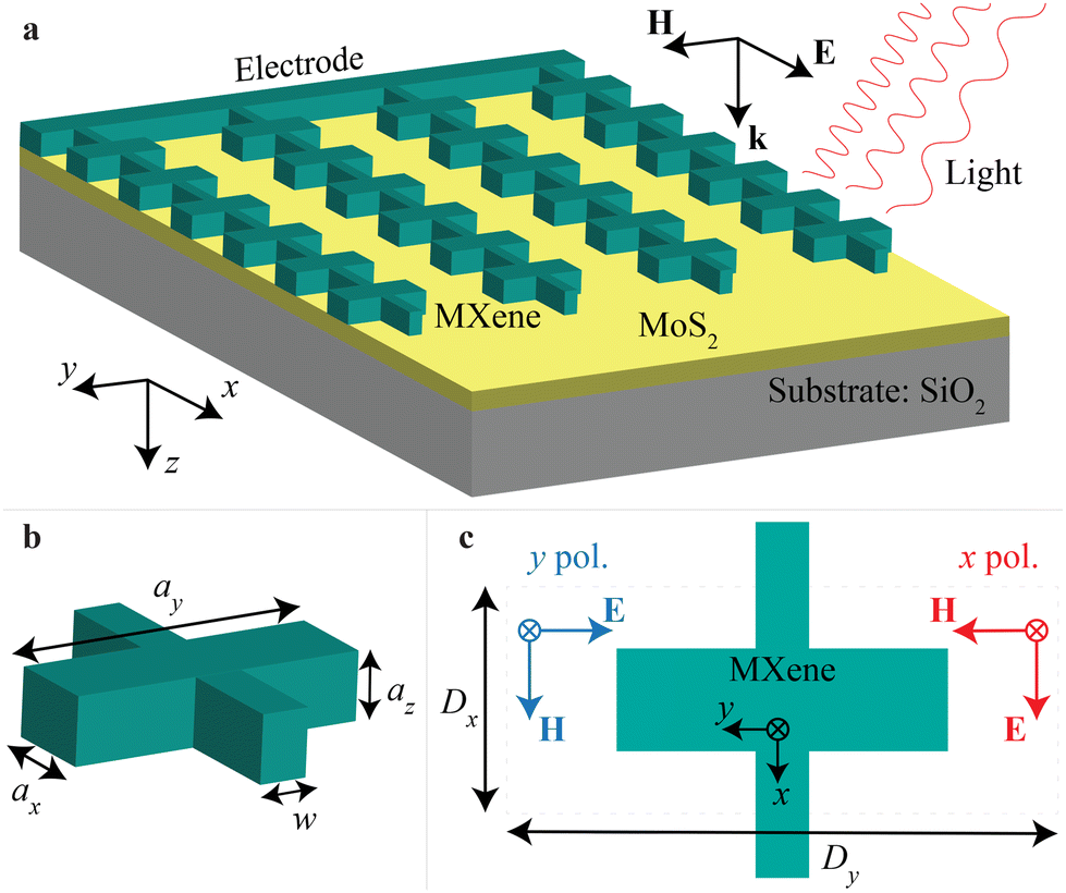 | ||
| Fig. 1 (a) Electrode schematic: MXene (Ti3C2Tx) resonant antennas (dark green) on the few-layer MoS2 (yellow) and the silica substrate (grey). The antennas are interconnected by the ‘bridge’ and attached to the electrode strip at one end, thus forming a metasurface. (b) Schematic of an array unit cell with MXene antenna considered in the numerical simulations. The dimensions of the cuboid particle are ax, ay, and az. (c) Top view of the unit cell simulated under two different light polarizations: the red arrows are for the x-polarization, and the blue arrows are for the y-polarization. Dx and Dy are the periodicities in the x- and y-directions, respectively. The ‘bridge’ connects metasurface antennas in the x-direction and has width w in the y-direction. | ||
2. MXene antennas and lattice resonances
Single antenna response
First, we calculate the optical cross-sections of an isolated MXene antenna using the Mie theory, see Methods.51 Because the real part of MXene permittivity is negative in the considered spectral range, and the light does not penetrate significantly into the antenna. The optical response of the MXene antennas resembles one of the other lossy plasmonic materials with a localized surface plasmon resonance mainly outside the antenna. We perform calculations of absorption and scattering cross-sections for each multipole separately, and because of the limitations of analytical calculations, we can only perform such calculations for spherical antennas in a uniform environment. We observe that the enhanced absorption covers a broad wavelength range of ∼2 μm, which includes visible and near-infrared regions (Fig. S1 in ESI†). For the MXene antenna, the electric dipole (ED) and electric quadrupole (EQ) cross-section efficiencies are significantly greater than those of the magnetic types and exhibit their peaks at sphere radii of around 100–200 nm and 250–450 nm, respectively. Magnetic resonances are relatively weak because of the insignificant penetration of the electromagnetic field inside the MXene antenna and the inability of the particle to support an electric current circulating inside.Collective multipole excitations
Next, we consider an array of Ti3C2Tx MXene antennas under normal illumination with a plane wave polarized in the x-direction. Collective resonances in periodic arrays of antennas occur when the electromagnetic waves interact with the array's periodic structure, causing the antennas to respond to these excitations in a coordinated manner.52,53 The collective resonances in periodic arrays of antennas are highly dependent on the array's geometry, size, and composition and can be tuned by adjusting these parameters to achieve specific optical properties.54 These resonances result in enhanced electromagnetic fields within the array, which can be exploited for a variety of applications, such as sensing, spectroscopy, and light harvesting.The lattice resonance can result in a narrow absorption peak and enhancement in electron photoemission from each MXene antenna in the array.2 Analytical models offer an unparalleled understanding of the mechanisms of resonant response that are excited in antenna arrays. By identifying the most robust multipole, analytical models can assist in designing metasurfaces that maximize their performance (see Methods). We calculate EQ extinction cross-section for various Dy while keeping Dx = 1500 nm (Fig. 2a). We see that EQ lattice resonance is excited in proximity to the Rayleigh anomaly and stays roughly unperturbed upon Dy changes. Excitation of EQ lattice resonance allows for a significant increase of absorption in an array of MXene antennas, which we explore next.
 | ||
| Fig. 2 Resonance response in the MXene-scatterer lattice: (a) EQ extinction cross-section, (b) Absorption, and (c) reflection. The data are acquired through the comprehensive numerical simulations of sphere antennas within the rectangular lattice. The results are shown for the changes in Dy and constant Dx = 1500 nm. The surrounding environment is free space with n = 1. The solid cyan lines ‘RA’ denote the Rayleigh anomaly wavelength in the free space (λRA = Dx, y). The sphere's size is R = 450 nm. Green circles denote the regions of enhanced absorption and generalized lattice Kerker effect in panels b and c, respectively. | ||
Absorption and Kerker effect
As previously stated, MXene antennas primarily support ED and EQ resonances, which can be amplified through the effective design of the antenna lattice. These two multipoles mainly define total absorption in the metasurface, and one can see a significant enhancement of absorption for Dy = 1500 nm (Fig. 2b).The mutual compensation of the ED and EQ multipole resonances, resulting in the suppression of reflection, is known as the generalized lattice Kerker effect.55 While ED resonance moves along with the Rayleigh anomaly upon Dy change, it crosses EQ resonance that is excited at λ ≈ 1500 nm. It results in a suppression of reflection for λ ≈ 1600–1700 nm and Dy < 1500 nm (Fig. 2c). Thus, we observe the generalized lattice Kerker effect because of the compensation of ED and EQ resonances. One can benefit from this reflection suppression and use it for efficient directional scattering and enhanced light absorption in the layer underneath the antenna metasurface. We choose to work with an array with Dx = Dy = 1500 nm in the further analysis of MXene antennas with a more realistic, lithographically defined shape on a substrate. In the following sections, we will employ a periodic configuration of MXene antennas to attain higher resonances and utilize this metasurface to create an electrode composed of MXene antennas.
3. Photodetector design
Hot-electron photodetector employing MXene as the material for photon absorption and MoS2 for electron conduction takes advantage of hot-electron generation when light photons are absorbed in MXene. This photodetector is designed based on the following principles. The process begins with the generation of hot electrons as a result of photon absorption in MXene, and the fundamental operation revolves around the absorption of light photons by the MXene layer. When these photons are absorbed, they impart their energy to electrons within MXene, creating what are known as hot electrons. These hot electrons possess significantly higher energy levels than their surrounding. To ensure that recombination is minimized, which can lead to the loss of hot electrons, the photodetector incorporates mechanisms such as a built-in electric field within the MXene material. In addition to that, the heterostructure that includes MoS2 layer plays a crucial role in directing the flow of hot electrons.MXene is chosen as the hot-electron generation and electrode material for its high absorption coefficient within the desired spectral range and its unique electronic properties. The separated hot electrons are effectively channeled to an electrode using the excellent electron-conducting properties of MoS2. This process results in the creation of a photocurrent, which is directly proportional to the number of hot electrons generated and, consequently, the intensity of the incident photons. To make the weak photocurrent generated by a limited number of hot electrons detectable, amplification techniques, such as electronic amplification or multiple stages of hot electron generation, need to be employed. Hot-electron photodetectors featuring MXene and MoS2 offer distinct advantages, particularly when incident photons have energies lower than the bandgap of traditional photodetectors, resulting in enhanced sensitivity and performance.
Above bandgap
The two-dimensional semiconductor molybdenum disulfide MoS2 belongs to the class of transition metal dichalcogenides. The broader detection range and better light absorption have made the few-layer MoS2 a great candidate for a high-performance photodetector. Compared to monolayer MoS2, few-layer MoS2 has better electric conductance and larger dark current.56 Typically, in a MoS2 photodetector, photocurrent is produced when the energy of incoming light exceeds the bandgap of MoS2. For a few-layer MoS2, the bandgap is at around 1.65 eV (wavelength ≈750 nm), and in general, it depends on the layer thickness.57,58 When illuminated with photons whose energy is lower than the bandgap, MoS2 does not undergo direct photon absorption. In the case of multilayer MoS2, it exhibits an indirect bandgap characteristic, which means that direct photon absorption does not occur, even when the photon energy exceeds the bandgap energy until the direct electronic transitions are reached. Due to the bandgap, the infrared spectral range does not generate significant photocurrent in MoS2.Below bandgap
As we discussed earlier, hot electrons can be ejected from metals illuminated by light and can play a crucial role in enhancing the functionality of photodetectors. Recently proposed photodetector designs include nanostructures with a channel layer adjacent to a metal surface that supports surface plasmon excitations. The non-radiative decay of plasmons results in the generation of hot electrons. The enhancement of the photocurrent in the photodetector is facilitated by the transfer of hot electrons from the metal to the channel layer over a Schottky barrier. More efficient transfer of hot electrons to the channel layer can be made possible by a smaller work function of the contact electrode and a lower Schottky barrier height, while the thermal effects negatively affect the efficiency. Despite being illuminated with light energy below its bandgap, the structure still generates photocurrent, and metal–semiconductor hybrid designs can further improve photodetector performance. Such hybrid photodetectors with a high-mobility two-dimensional semiconductor channel and plasmonic structured metal have extensively been studied and demonstrated high potential for practical applications.59,60We propose a photodetector electrode design based on an interconnected array of the MXene antennas (Fig. 1). The lattice effects play a crucial role in the excitation of strong resonances and enhancement of absorption in the periodic array of antennas. The two-dimensional semiconductor molybdenum disulfide MoS2 layer underneath MXene antennas is utilized for hot-electron transport further into the circuit, which results in a peak value in an internal photogain.61,62 The work functions of MoS2 and MXene materials have been reported earlier in the literature but with a significant discrepancy in the values.63–66 Here, we show that hot-electron generation can be significantly improved by using MXene antennas instead of a continuous stripe. Placement of MXene antennas in the regular array results in the lattice resonances that are essential in overcoming antenna losses and enhancing the structure resonances.
Electric field enhancement and hot-electron generation
The surface nature of MXene resonances limits the field penetration, resulting in weaker magnetic resonances in both theoretical calculations and simulations of electromagnetic field profiles. In contrast to dielectric particles, which confine Mie resonances within the particle, the field distribution of MXene antennas is mainly localized outside the particle. As a result, the surrounding medium's refractive index is crucial for controlling the resonances’ spectral positions and strength. This observation highlights the significant impact of the surrounding index on resonance control compared to antenna shape and size. Our analytical calculations reveal the conditions required for ED and EQ resonance excitation, and the numerical simulations confirm the electromagnetic fields’ primary localization outside the antenna (see Fig. S2 in the ESI†), in agreement with the above considerations.Owing to the gained kinetic energy, hot electrons can move into other surrounding materials over the potential barriers at the boundaries through injection or tunneling.42 Hot carriers are generated in a photodetector through both bulk and surface mechanisms, with the latter being more dominant in the near-infrared range.45 In the bulk mechanism, the hot-electron photoemission rate is proportional to the local absorption of light inside the particle, i.e.,
 | (1) |
In the surface mechanism, the photoemission rate is proportional to the square of the normal component of the electric field, i.e.,67,68
 | (2) |
4. Narrowband photodetector
Let's consider the design of the MXene electrode for a narrowband photodetector. In this part, we show how MXene resonant response changes upon transforming a continuous strip into an array of interconnected antennas. We use lattice excitations in the periodically arranged antennas to increase light absorption inside the electrode.Analytical calculations presented above provide an important insight into the properties of the MXene antenna array. They allow for the identification of the nature of each resonance (electric or magnetic, dipole or quadrupole) and provide a guideline for engineering electrode properties. However, the analytical calculations have been developed only for an infinite lattice of identical spherical particles in a uniform environment. In practice, the electrode must be based on lithographically-defined antennas (e.g., disk or cuboid) that rest on a substrate. To account for more realistic designs, we also need to include a thin MoS2 channel underneath antennas and employ full-wave numerical simulations for accounting for other properties of the realistic structure (see Methods).
We identify the regime for the largest excitation of resonances based on the array parameters and antenna shapes. We analyze the response of arrays of MXene antennas with lithographically-defined shapes but with other parameters close to those of the sphere arrays analyzed analytically. For the comparable array dimensions, the cube, cuboid, and disk arrays with the size of 700 nm have relatively greater absorption than the sphere with 2R = 900 nm, as shown in Fig. S3 in the ESI.†
To consider practically, lithographically-defined structure, we calculate the response of a cube array with sides of ax = ay = az = 700 nm, which are connected to each other in the x-direction (Fig. 3). The absorption spectra are obtained with full-wave numerical simulations. As previously discussed and illustrated by eqn (1), the photoemission volume mechanism is primarily determined by the total light absorption within the antenna. Thus, the spectral regions with increased absorption correspond to enhanced hot electron generation.
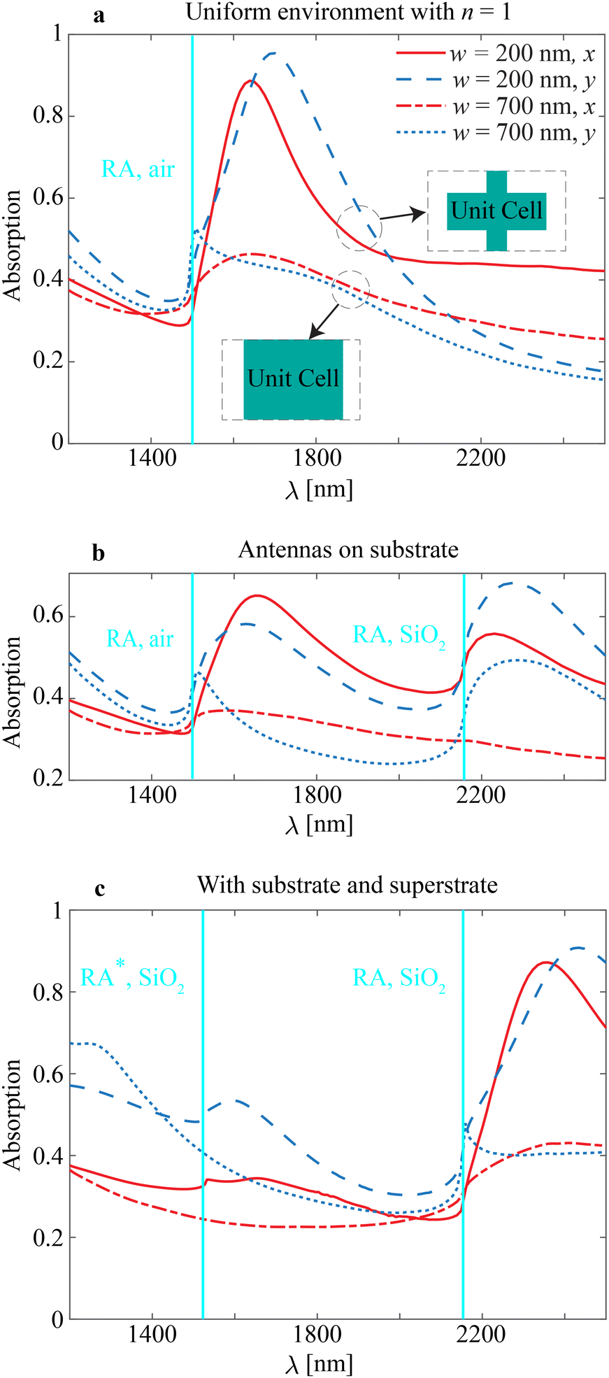 | ||
Fig. 3 Light absorption as a contribution to the volume mechanism of the hot-electron generation through resonant excitations in the interconnected MXene antennas arranged in the periodic array (metasurface): (a) antennas in the uniform surrounding with n = 1, (b) on a few-layer MoS2 and SiO2 substrate, and (c) on a few-layer MoS2 and SiO2 substrate with an index-matching superstrate. We consider MXene antennas of cube shape with ax = ay = az = 700 nm connected with ‘bridges’ with the width of w = 200 nm or 700 nm. The latter corresponds to the continuous stripes. Notations ‘x’ and ‘y’ correspond to the illumination of light with the x- or y-polarization (see Fig. 1c). The antennas are arranged into a periodic lattice with periods Dx = Dy = 1500 nm. The solid cyan lines denote the Rayleigh anomaly wavelengths: ‘RA, air’ denotes the Rayleigh anomaly in the free space (λRA, air = Dx, y), and ‘RA, SiO2’ denotes the Rayleigh anomaly in SiO2 (λRA, SiO2 = nSiO2Dx, y), correspondingly. ‘RA*, SiO2’ denotes a next-order Rayleigh anomaly at  . . | ||
In Fig. 3a, we show the response of the cube array interconnected in the x-direction with symmetric periodicities of Dx = Dy = 1500 nm under the illumination with light polarized either in the x- or y-directions. The first set of plots in Fig. 3a shows the resonance when the array elements are connected with bridges of w = 200 nm. The second set of plots shows that the absorption resonance weakens when the bridge width is extended to w = 700 nm. One can notice that maximum absorption occurs on the red side from the wavelength that corresponds to the Rayleigh anomaly in the free space (denoted as ‘RA, air’ in Fig. 3a). Resonant excitations in the interconnected MXene antennas for ‘bridges’ with the width of w = 100 to 700 nm by the step of 100 nm are shown in Fig. S4 in ESI.† One can see that the absorption peak decreases as the bridge width widens, and the resonance almost vanishes.
Next, we consider a more practical case and include a substrate and channel layer into account: we perform numerical simulations with a silica substrate and 3 nm-thick MoS2 layer (Fig. 3b). The real and imaginary parts of MoS2 and silica permittivity are obtained from the literature.71,72 The substrate introduces a half-space with a distinct refractive index beneath the antenna array. This distinct refractive index results in an additional Rayleigh anomaly that corresponds to diffraction order transition in the corresponding half-space. As a result, introducing the substrate and MoS2 layer results in additional spectral features. In particular, due to the substrate, we see an additional peak appearing spectrally close to the Rayleigh anomaly in SiO2 denoted as ‘RA, SiO2’ in Fig. 3b. Absorption peaks are diminished in comparison to the free-space case and get down to ≈0.6. The spectra on panel (b) are also affected by the 3 nm-thick MoS2 layer, but this inclusion does not result in additional Rayleigh anomaly because of the small layer thickness.
An asymmetric refractive-index environment has been known to reduce lattice resonances. Therefore, the most optimal structure for the excitation of lattice resonances includes not only substrate but also index-matching superstrate. In this study, we consider a superstrate with a refractive index of silica and keep all other array parameters as before. From Fig. 3c, we see that adding the silica superstrate enhances resonances in the proximity to ‘RA, SiO2’, and the peak values of array absorption reach 0.9. The structure is advantageous for designing photodetectors in the wavelength range of about 2.2–2.4 μm. The structures with index-matching superstrates also exhibit spectral features in the proximity to the next-order Rayleigh anomaly73 at  (denoted ‘RA*, SiO2’ in Fig. 3c).
We observe that a structured MXene layer enhances absorption several times in comparison to the continuous stripes. As a result, hot-electron generation from both surface and volume mechanisms can be significantly enhanced and enable the operation of the photodetector for the photon energies below the bandgap.
The MXene antennas form the photonic structure that is antisymmetric with respect to two lateral (in-plane) axes. Similar to the array of optical antennas made of noble metal,74 this structure can provide wavelength and polarization selectivity. The extensive design flexibility of the antenna array can be utilized to enhance the photodetector's optical properties. Having two different array periodicities, the photodetector can be designed to resonantly enhance photoresponse at two distinct target wavelengths, while each of them is determined by the orientation of the orthogonal polarization of the incoming light. This results in the photodetector's versatile capabilities for applications in spectrally selective and polarization-resolved imaging. Such an approach proves advantageous for advancing the development of ultracompact, cost-effective, and multi-functional optoelectronic sensors. The advantage of metamaterial-based polarization- and wavelength-selective designs has been demonstrated in ref. 74 for terahertz photodetector. Here, we demonstrate the properties of selectivity for the MXene-based photodetector in the near-infrared spectral range. In Fig. 3, we observe polarization-sensitive absorption, where the antenna array shows different responses to the x- and y-polarizations. This occurs because the collective effects responsible for the excitation of strong resonances depend on the array period in a specific direction. Specifically, when illuminated with x-polarization, ED is sensitive to the array periodicity in the y-direction, while EQ is sensitive to the array periodicity in the x-direction. Conversely, for y-polarized incident light, the sensitivity is reversed. These properties make the antenna array a functional element for polarization- and/or wavelength-selective photodetectors.
As discussed earlier, generation of hot electrons can be attributed to two competing causes of the photoelectric effect, namely surface and volume mechanisms. The efficiency of the volume mechanism is determined by the total loss of optical power in the antenna. Similarly, the enhancement of the normal electric field at the surface inside the antenna Eω,normal/E0, squared and averaged over the antenna surface immediately adjacent to the MoS2 defines the efficiency of the surface mechanism (see eqn (2), which primarily determines the photoemission rate). Absorption in the MXene antenna array in Fig. 3 predicts the efficiency of hot electron generation through the volume mechanism. As a counterpart, in Fig. 4a, we calculate the wavelength dependence of (Eω,normal/E0)2 averaged over the MXene/MoS2 interface in the arrays with two different bridges, w = 200 or 700 nm, either in the case of free-space surrounding or index-matching superstrate (here, Eω,normal = Ez).
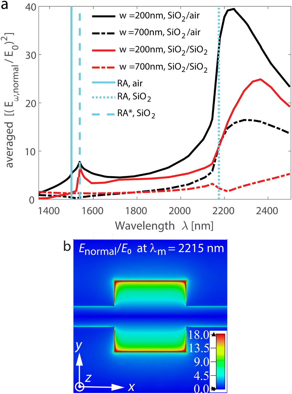 | ||
Fig. 4 Enhancement of the normal electric field at the surface of the particle. This field enhancement determines the surface mechanism of the hot-electron generation. (a) Eω, normal/E0, squared and averaged over the particle surface immediately adjacent to the MoS2. Antennas have a cuboid shape with ax = ay = az = 700 nm and bridge width w = 200 or 700 nm. Antennas are placed on a few-layer MoS2 and SiO2 substrate. Notations ‘SiO2/air’ and ‘SiO2/SiO2’ correspond to the case when antennas are uncovered (in free space) and covered with an index-matching superstrate (refractive index of glass SiO2), respectively. The array is illuminated with the y-polarized light. The antennas are arranged into a periodic lattice with periods Dx = Dy = 1500 nm. The vertical cyan lines denote the Rayleigh anomalies as follows: the solid line ‘RA, air’ is for the free space (λRA, air = Dx, y), the dotted line ‘RA, SiO2’ is for the silica (λRA, SiO2 = nSiO2Dx, y), and the dashed line ‘RA*, SiO2’ is for the next-order Rayleigh anomaly in silica at  . (b) Eω, normal/E0 distribution at the bottom surface of the unit cell. Antenna array parameters are ax = ay = az = 700 nm, w = 200 nm, Dx = Dy = 1500 nm, antennas are uncovered, and illuminated with y-polarized light (solid black line in panel a). The wavelength of the field distribution is λm = 2215 nm, which corresponds to the maximum of Eω, normal/E0 averaged over the antenna surface. . (b) Eω, normal/E0 distribution at the bottom surface of the unit cell. Antenna array parameters are ax = ay = az = 700 nm, w = 200 nm, Dx = Dy = 1500 nm, antennas are uncovered, and illuminated with y-polarized light (solid black line in panel a). The wavelength of the field distribution is λm = 2215 nm, which corresponds to the maximum of Eω, normal/E0 averaged over the antenna surface. | ||
The averaged enhancement of the normal electric field at the surface inside the antenna Eω,normal/E0 is up to 40 and the highest for the case of uncovered antennas with the narrow bridges of w = 200 nm (Fig. 4a). In agreement with absorption calculations, the field enhancement inside the MXene antenna decreases with an increase in the bridge width (compare solid and dash-dot lines), going down to ∼16 for uncovered antennas. Unlike the trend observed when analyzing absorption with and without an index-matching superstrate, uncovered antennas exhibit higher normal electric field values inside the antenna at the interface, as shown by the comparison of the black and red solid lines. Thus, the narrow bridge between antennas yields values no greater than 25. Eω,normal/E0 distribution at the bottom surface of the unit cell indicates that the strongest field enhancement is at the antenna boundaries, and it gradually decreases towards the center of the antenna (Fig. 4b). The enhancement of the electric field can be attributed to the reflection at the interface facilitated by the silica substrate and few-layer MoS2, which results in an increase in the field intensity. From Fig. 4a, we see that the field is substantially enhanced in the proximity to the Rayleigh anomalies in the silica (λRA,SiO2 = nSiO2Dx, y) for all but one cases. It indicates that the periodic arrangement and narrowing of the bridge play a key role in enhancing hot electron generation. Silica's contribution is more significant for the surface mechanism than for the volume mechanism. Since the uncovered array exhibits greater enhancement in the surface mechanism, we have chosen it for further experimental proof-of-concept demonstration.
Fig. 5 demonstrates the experimental resonant response of the periodic array of titanium antennas with cuboid shape, ax = ay = 600 nm and az = 400 nm dimensions, bridge width w = 200 nm, and array periodicities Dy = Dx = 1500 nm (see Methods). The spectrometer photodetector limit is 2.15 μm, thus determining the specter of the measurements. We observe a good agreement with numerical simulations and results for Ti3C2Tx. In practical scenarios, designing metasurfaces with thinner antennas is feasible and beneficial. However, it is essential to consider that using thinner antennas may impede the efficient excitation of quadrupole resonances in such metasurfaces.
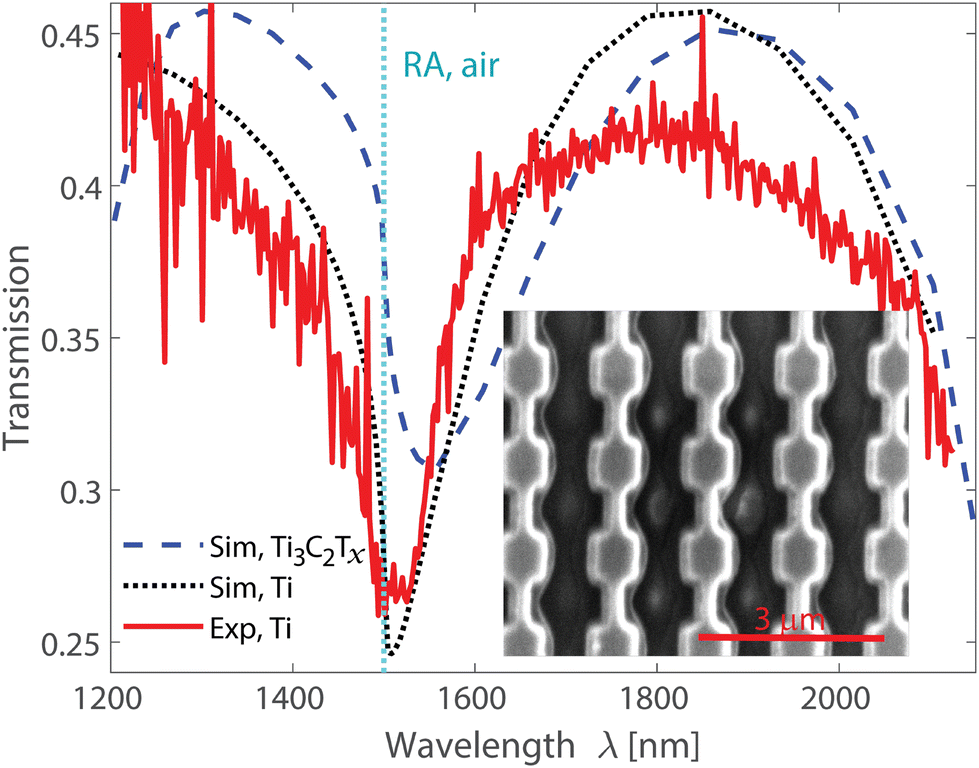 | ||
| Fig. 5 Proof-of-concept experimental characterization of the collective response in the lattice of lossy cuboids. Inset: scanning electron microscope image of the fabricated metasurface. Antennas have a cuboid shape with ax = ay = 600 nm, az = 400 nm, and bridge width w = 200 nm. Notations ‘Sim’ and ‘Exp’ correspond to the numerical simulation and experimental measurement, respectively. The metasurface is fabricated on a fused silica substrate. The metasurface is illuminated with the y-polarized light. The antennas are arranged into a periodic lattice with periods Dx = Dy = 1500 nm. The solid cyan line ‘RA, air’ denotes the Rayleigh anomaly in the free space (λRA, air = Dx, y). | ||
Antennas made of lossy materials typically exhibit many similarities in their properties, with the collective properties of the array mainly defining its overall response. As a result, the properties of individual antennas have less of an impact on the array's behavior.75,76 In the case of the Ti lattice, the measurements show a substantial transmission decrease next to the Rayleigh anomaly, corresponding to the collective resonances of the array. This phenomenon is caused by the constructive interference of the scattered fields from individual antennas. It is worth noting that the collective properties of lossy antennas can also give rise to various applications. Such metasurfaces can also be used as absorbers, with the collective resonances enhancing the absorption of incident light. MXene, due to its unique properties, such as high conductivity, high carrier mobility, and large surface area, can enhance absorption and carrier transport in photodetectors.
MXenes pose significant challenges in the process of fabricating lithographically-defined metasurfaces. Addressing these challenges is essential to determine whether the benefits of MXene metasurfaces justify the efforts required in their nanofabrication. Additionally, it is crucial to assess whether MXenes offer advantages over noble metals, titanium, and other lossy metals, making them a worthwhile pursuit in the field of metasurface research.
Finally, we note that for practical reasons outlined below, we use titanium for our proof-of-concept experimental characterization instead of other materials, such as nickel or chromium. One of the primary reasons for choosing titanium is its similarity to the MXene material in terms of permittivity values and conductivity. Titanium and MXene both exhibit lossy characteristics, which means they dissipate electromagnetic energy to a similar extent. This similarity ensures that the experimental results obtained using titanium are more representative of the behavior we expect from MXene, making the findings more directly applicable to our research objectives. Furthermore, from a practical point of view, recipes for the titanium nanofabrication procedure are readily available in our cleanroom, which made it a reasonable choice for our proof-of-concept experiments. Thus, the decision to use titanium for our proof-of-concept characterization is grounded in its similarity to MXene in terms of permittivity values and its practicality due to the ready availability of nanofabrication. By choosing titanium for the antenna material, we aim to ensure that the experimental results closely reflect the expected behavior of MXene.
5. Broadband photodetector
In the previous section, we show how the transformation of a non-resonant strip (conventional electrode) into a resonant electrode (array of interconnected antennas) can lead to significant changes in the spectral response. The periodic arrangement of the strip structuring and light confinement significantly enhances the absorption. The concept can be generalized to construct an MXene antenna array with varying periodicities, as shown in Fig. 6a. Each patch is part of an electrode with distinct periods Dx(n) and Dy(n), and the lattice resonance can be excited at a particular wavelength corresponding to that period. The complex resonant electrode of the two-dimensional multiple-period array of interconnected MXene antennas is designed to enhance photoemission across a broad spectrum due to the lattice resonances occurring at different wavelengths. | ||
| Fig. 6 (a) Schematic of the resonant electrode of a two-dimensional multiple-period interconnected array of the MXene antennas. Each color represents a patch with a distinct pitch based on periodicities of Dx(n) and Dy(n) from 1 to n. This electrode enables enhanced photoemission across a broad spectrum of wavelengths. (b) Resonant excitations in finite-size array consisting of the 7 × 7 = 49 interconnected MXene antennas. We consider MXene antennas of cube shape with ax = ay = az = 700 nm connected with ‘bridges’ with the width of w = 200 nm or 700 nm. The latter corresponds to the continuous stripes. Notations ‘x’ and ‘y’ correspond to the illumination of light with x- or y-polarization (see Fig. 1c). The cuboids are placed into a regular array with pitches Dy = Dx = 1500 nm. Antennas are in the uniform surrounding with n = 1. The absorption cross-section spectra are obtained with full-wave numerical simulations. The solid cyan line denotes the Rayleigh anomaly wavelengths: ‘RA, air’ denotes the Rayleigh anomaly in the free space (λRA, air = Dx, y). | ||
Earlier works have demonstrated that 49 (7 × 7) particles in a finite-size array are sufficient to excite spectral lattice features, similar to the case of an infinite array.75 In other words, the array of 7 × 7 particles can support resonances comparable to those in the infinite particle array, and we use it in further analysis. Fig. 6b shows the resonant excitations in a finite-size array of the interconnected MXene antennas. It is a finite-size version of Fig. 3a, which are similar qualitatively. While Fig. 3 shows an absorbed portion of light in the infinite array, Fig. 6b represents an absorption cross-section measured in μm2. Here, instead of analyzing absorption, we are investigating the absorption scattering cross-section. This is because absorption cannot be defined in the case of an array with a finite number of particles. Thus, a direct quantitative comparison is not possible. In this case, we observe that 7 × 7 antenna array supports the excitations of lattice resonances, and the similarity can be shown in other cases as well.
Collective resonances in infinite and finite periodic arrays are similar in that they arise due to the interaction between the periodic structure and the surrounding environment. The strength of collective resonances in infinite and finite periodic arrays can depend on various factors, such as the size of the periodic structure, the surrounding environment, and the frequency of excitation. In general, collective resonances in infinite arrays can exhibit stronger coupling with the environment and stronger field enhancement compared to finite arrays due to the absence of boundaries and the presence of an infinite number of resonators. However, the resonance strength can also be influenced by the specific parameters of the arrays and the desired application.
Within the engineered structure of the two-dimensional interconnected MXene antenna array, a complex resonant electrode has been designed to significantly boost photoemission across a wide spectrum of wavelengths. This enhancement is achieved by harnessing the lattice resonances that manifest at distinct wavelengths depending on the array periodicity. Each constituent patch within such a designed array represents a unique electrode. The uniqueness of this approach lies in its ability to selectively excite lattice resonances at precisely matching wavelengths corresponding to these individual periods. In essence, this means that each distinct period acts as a tuning mechanism for the array, allowing it to operate with exceptional efficiency across a broad range of wavelengths.
By using the lattice resonances, the interconnected MXene antenna array overcomes the limitations of traditional designs with single-period arrays. It becomes a powerful tool for harnessing and manipulating electromagnetic waves, making it particularly suitable for applications requiring broadband photoemission enhancement. Thus, the interconnected MXene antenna array, with its multiple periods and lattice-resonance-driven design, proves itself to be a practical solution for efficiently enhancing photoemission across a broad range of wavelengths.
6. Discussion
Our research focuses on nanostructured MXene layers, specifically tailored for designing photodetector electrodes and enhancing their response through hot-electron generation. Despite their potential in electronic applications, it is important to address concerns regarding the stability of MXene materials in ambient environments where practical applications would inevitably operate. Experimental investigations assessing material stability under various environmental conditions, such as humidity, temperature, and exposure to oxygen, are vital steps toward bridging the gap between theoretical predictions and realistic practical cases.In ref. 77, to achieve molecular bridging, an effective strategy employs tannic acid rich in oxygen ligands. Thus, the tannic acid self-polymerizes and forms bonds with terminal groups and exposed titanium atoms in Ti3C2Tx through hydrogen and coordination bonds. This enhances interlaminar interaction, rendering the MXene film resistant to oxidation, swelling, and mechanical fragility. In ref. 78, the environmental instability of MXene-Ti3C2Tx has been successfully overcome through an optimized synthetic route, which has included the synthesis of high-quality MAX phase (Ti3AlC2) and post-treatment of Ti3C2Tx. This optimization has yielded highly stable O-Ti3C2Tx. Notably, at the reduced concentrations of ∼0.1 mg mL−1, the dark green aqueous dispersion of monolayer O-Ti3C2Tx has shown no signs of oxidation or degradation. Furthermore, a cation assembly procedure has been shown in ref. 79 for the realization of exceedingly stable multilayered films using V2CTx and Ti2CTx MXenes, originating from their chemically unstable delaminated monolayer flakes. In short, various strategies, including cation-driven assembly and oxygen-rich molecular bridging, offer promising avenues for enhancing MXene stability, reaffirming its potential as a valuable material in the development of high-performance photodetectors.
7. Conclusion
We demonstrated the existence of collective resonances in an array of Ti3C2Tx MXene antennas and investigated the interplay between different multipole modes in the structures with varying periodicities. The periodic arrangement of antennas greatly enhances these multipole resonances, resulting in stronger light–matter interactions. We showed a significant enhancement in light absorption attributed to the periodic characteristics of the proposed MXene metasurface. The amplified absorption properties of the interconnected MXene antenna array enable the generation of hot electrons, making the proposed photodetector electrode composed of these antennas a viable option. We conducted nanofabrication procedures and performed proof-of-concept measurements to observe the resonant peak in the interconnected array of titanium antennas. Our experimental results are in good agreement with the full-wave numerical simulations. The utilization of this design enables the efficient generation of hot electrons upon exposure to light. This design offers significant advantages when the structure is exposed to photons with energies lower than the bandgap of the semiconductor used as the channel medium. Our analysis suggests that a two-dimensional multiple-period array of interconnected MXene antennas may enhance the functionality of hybrid plasmonic devices, widen the operational band, and augment sensitivity.8. Methods
Ti3C2Tx permittivity
Titanium carbide Ti3C2Tx has a complex permittivity with a large negative real part and a large imaginary part (Fig. S5 in ESI†). The material has losses, and it corresponds to a positive value of the imaginary part in our analytical model (i.e., we use eikr term for wave propagation).Analytical calculations
Absorption and scattering cross-sections were calculated using Mie theory, see ref. 51 and 80 for details. The analytical models for a periodic array of spherical particles have been developed in earlier works.55,75 Calculations of the optical response of the infinite lattice consisting of multipoles were derived through coupled dipole–quadrupole equations (schematic is shown in Fig. S6 in ESI†). The effective polarizabilities of each multipole were derived from lattice contribution using lattice sums. These calculations include single-particle polarizabilities derived from Mie theory up to magnetic quadrupole and effective particle polarizability accounting for the lattice sums and cross-multipole coupling.One can relate the effective polarizability of the particle in the array and intrinsic optical properties of the particle material (such as the real and imaginary parts of the permittivity). As discussed in the ESI (Fig. S7†), the effective polarizabilities of ED and EQ can be used to tune the multipole resonances to the desired spectral position. Such tuning the resonant response of the MXene antenna arrays and engineering array designs allows for achieving higher field enhancement and hot-electron generation.
Numerical simulations
We used a frequency-domain solver implemented in the commercial package CST Studio Suite. In the full-wave numerical simulations, we considered one particle in the unit cell, periodic boundary conditions in the x- and y-directions, perfectly matched layers in the z-direction, and normal incidence of light. MXene antenna, MoS2 layer, and silica substrate (if present) were considered dispersive.Uncertainty in MXene permittivity
The permittivity of MXenes materials changes depending on the number of layers in a few-layer case or the total thickness of the thicker layers. Considering possible variations in the Ti3C2Tx permittivity, we perform calculations for the different values and array parameters obtained above. We confirm that the absorption profiles of the structure do not alter drastically under variation of the permittivity (Fig. S5 in ESI†). The approach can be generalized to other shapes of antennas and other MXene materials.Nanofabrication
Fused silica sample of 1 cm × 1 cm was cleaned and spin-coated for e-beam exposure in the following way: HMDS was spin-coated at 2000 rpm; PMMA 950-A9 was spin-coated with 5000 rpm and baked at 180 °C for 3 min; PMMA 950-A9 was spin-coated, but this time with 3000 rpm and baked at 180 °C for 3 min; finally, ‘Discharge’ solution was spin-coated twice with 4000 rpm. This gives ∼2.8 μm-thick layer of e-beam resist. ‘Discharge’ is needed to increase the conductivity of the sample when working with non-conductive substrates, such as fused silica. Electron-beam exposure was performed with JEOL JBX 6300-FS, 60 μm aperture, 100 kV energy, and 1 nA current. These conditions give an e-beam spot down to ∼7.5 nm. The total array area is 900 μm × 900 μm, allowing sufficient area for measurement. After the exposure, the ‘Discharge’ layer was removed by rinsing in deionized water. The sample was developed in MIBK/IPA 1![[thin space (1/6-em)]](https://www.rsc.org/images/entities/char_2009.gif) :3 solution for 90 s and rinsed with IPA. Titanium deposition was performed with an electron gun (e-beam evaporator) with a 0.5 Å s−1 rate to the total thickness of 400 nm. The sample was kept in Remover PG heated to 78 °C for 2 h 30 min, and subsequently, the liftoff was performed by a thorough rinse with acetone, cleaning with an acetone gun, and a final quick rinse with IPA. The lateral dimensions of the antennas are taken with a scanning electron microscope. Out of the first 20 attempts, ten samples met the criteria for dimensions and measurement, and subsequent characterization of a few samples yielded consistent results (Fig. S8 in ESI†). The initial challenges related to e-beam exposure and resist thickness, as well as occasional issues with e-beam spin-coating uniformity, were overcome.
:3 solution for 90 s and rinsed with IPA. Titanium deposition was performed with an electron gun (e-beam evaporator) with a 0.5 Å s−1 rate to the total thickness of 400 nm. The sample was kept in Remover PG heated to 78 °C for 2 h 30 min, and subsequently, the liftoff was performed by a thorough rinse with acetone, cleaning with an acetone gun, and a final quick rinse with IPA. The lateral dimensions of the antennas are taken with a scanning electron microscope. Out of the first 20 attempts, ten samples met the criteria for dimensions and measurement, and subsequent characterization of a few samples yielded consistent results (Fig. S8 in ESI†). The initial challenges related to e-beam exposure and resist thickness, as well as occasional issues with e-beam spin-coating uniformity, were overcome.
Measurements
Transmission measurement was performed using a custom setup connected to Ocean Optics NIRQuest + 2.2 spectrometer operating in the range 0.9–2.15 μm with a resolution of ∼5.5 nm. The sample was illuminated with broadband light propagating through a series of optical elements and lenses for focusing on a spot down to ∼100 μm in diameter. A small aperture was placed between the last focusing lens and the sample to allow only light normal to the sample with not more than ∼1° deviation. Transmission through the array was normalized to the transmission through the sample spot without any antennas.Abbreviations
The following acronyms and abbreviations are used in this work:
| ED | Electric dipole |
| EQ | Electric quadrupole |
| MXene | Mn+1XnTx, ‘M’ is the transition metal, ‘X’ is either C and/or N, and ‘T’ is the surface functional group |
| RA | Rayleigh anomaly |
Conflicts of interest
There are no conflicts to declare.Acknowledgements
V. E. B. acknowledges the support from the University of New Mexico Research Allocations Committee (Award No. RAC 2023) and WeR1: Investing in Faculty Success Programs SURF and PERC. This work was performed, in part, at the Center for Integrated Nanotechnologies, an Office of Science User Facility operated for the U.S. Department of Energy (DOE) Office of Science by Los Alamos National Laboratory (Contract 89233218CNA000001) and Sandia National Laboratories (Contract DE-NA-0003525). The work was also supported by Contract DE-2375849.References
- A. D. Utyushev, V. I. Zakomirnyi and I. L. Rasskazov, Rev. Phys., 2021, 100051 CrossRef.
- S. V. Zhukovsky, V. E. Babicheva, A. V. Uskov, I. E. Protsenko and A. V. Lavrinenko, Plasmonics, 2014, 9, 283–289 CrossRef CAS.
- K. Baryshnikova, M. I. Petrov, V. E. Babicheva and P. A. Belov, Sci. Rep., 2016, 6, 1–11 CrossRef PubMed.
- W. Zhou, M. Dridi, J. Y. Suh, C. H. Kim, D. T. Co, M. R. Wasielewski, G. C. Schatz and T. W. Odom, Nat. Nanotechnol., 2013, 8, 506 CrossRef CAS PubMed.
- V. E. Babicheva, S. Gamage, M. I. Stockman and Y. Abate, Opt. Express, 2017, 25, 23935–23944 CrossRef CAS PubMed.
- P. Offermans, M. C. Schaafsma, S. R. Rodriguez, Y. Zhang, M. Crego-Calama, S. H. Brongersma and J. Gómez Rivas, ACS Nano, 2011, 5, 5151–5157 CrossRef CAS PubMed.
- V. Karimi and V. E. Babicheva, MRS Adv., 2021, 6, 234–240 CrossRef CAS.
- V. Karimi and V. E. Babicheva, Metamaterials, Metadevices, and Metasystems 2020, 2020, p. 114601F Search PubMed.
- S. Mubeen, J. Lee, W. Lee, N. Singh, G. D. Stucky and M. Moskovits, ACS Nano, 2014, 8, 6066–6073 CrossRef CAS PubMed.
- G. Baffou and R. Quidant, Laser Photonics Rev., 2013, 7, 171–187 CrossRef CAS.
- Z. J. Coppens, W. Li, D. G. Walker and J. G. Valentine, Nano Lett., 2013, 13, 1023–1028 CrossRef CAS PubMed.
- Y. Pan, G. Tagliabue, H. Eghlidi, C. Höller, S. Dröscher, G. Hong and D. Poulikakos, Sci. Rep., 2016, 6, 1–7 CrossRef PubMed.
- W. Li and J. Valentine, Nano Lett., 2014, 14, 3510–3514 CrossRef CAS PubMed.
- F. Qiao, Y. Xie, G. He, H. Chu, W. Liu and Z. Chen, Nanoscale, 2020, 12, 1269–1280 RSC.
- H. Yi, Y. Ma, Q. Ye, J. Lu, W. Wang, Z. Zheng, C. Ma, J. Yao and G. Yang, Adv. Sens. Res., 2023, 2, 2200079 CrossRef.
- Q. Wang, Z.-H. Ren, W.-M. Zhao, L. Wang, X. Yan, A.-s. Zhu, F.-m. Qiu and K.-K. Zhang, Nanoscale, 2022, 14, 564–591 RSC.
- C. M. Watts, X. Liu and W. J. Padilla, Adv. Mater., 2012, 24, OP98–OP120 CAS.
- C.-W. Cheng, M. N. Abbas, C.-W. Chiu, K.-T. Lai, M.-H. Shih and Y.-C. Chang, Opt. Express, 2012, 20, 10376–10381 CrossRef CAS PubMed.
- J. Hao, J. Wang, X. Liu, W. J. Padilla, L. Zhou and M. Qiu, Appl. Phys. Lett., 2010, 96, 251104 CrossRef.
- F. Ding, J. Dai, Y. Chen, J. Zhu, Y. Jin and S. I. Bozhevolnyi, Sci. Rep., 2016, 6, 1–9 CrossRef PubMed.
- W. Li, U. Guler, N. Kinsey, G. V. Naik, A. Boltasseva, J. Guan, V. M. Shalaev and A. V. Kildishev, Adv. Mater., 2014, 26, 7959–7965 CrossRef CAS PubMed.
- M. Chirumamilla, A. Chirumamilla, Y. Yang, A. S. Roberts, P. K. Kristensen, K. Chaudhuri, A. Boltasseva, D. S. Sutherland, S. I. Bozhevolnyi and K. Pedersen, Adv. Opt. Mater., 2017, 5, 1700552 CrossRef.
- H. Li, L. Wang and X. Zhai, Sci. Rep., 2016, 6, 1–8 CrossRef PubMed.
- Y. Long, L. Shen, H. Xu, H. Deng and Y. Li, Sci. Rep., 2016, 6, 1–8 CrossRef.
- W. Cai and V. M. Shalaev, Optical Metamaterials, Vol. 10( 6011), 2010 Search PubMed.
- S. A. Maier, Plasmonics: fundamentals and applications, Springer Science & Business Media, 2007 Search PubMed.
- M. Naguib, Nanomaterials Handbook, 2017, 2, 83–103 Search PubMed.
- J. Halim, S. Kota, M. R. Lukatskaya, M. Naguib, M.-Q. Zhao, E. J. Moon, J. Pitock, J. Nanda, S. J. May, Y. Gogotsi and M. W. Barsoum, Adv. Funct. Mater., 2016, 26, 3118–3127 CrossRef CAS.
- B. Anasori, M. R. Lukatskaya and Y. Gogotsi, Nat. Rev. Mater., 2017, 2, 1–17 Search PubMed.
- D. Zhang, D. Shah, A. Boltasseva and Y. Gogotsi, ACS Photonics, 2022, 9, 1108–1116 CrossRef CAS.
- K. Chaudhuri, Z. Wang, M. Alhabeb, K. Maleski, Y. Gogotsi, V. Shalaev and A. Boltasseva, in Optical Properties of MXenes, ed. B. Anasori and Y. Gogotsi, Springer International Publishing, Cham, 2019, pp. 327–346 Search PubMed.
- M. Alhabeb, K. Maleski, B. Anasori, P. Lelyukh, L. Clark, S. Sin and Y. Gogotsi, Chem. Mater., 2017, 29, 7633–7644 CrossRef CAS.
- K. Chaudhuri, M. Alhabeb, Z. Wang, V. M. Shalaev, Y. Gogotsi and A. Boltasseva, ACS Photonics, 2018, 5, 1115–1122 CrossRef CAS.
- Y. I. Jhon, J. Koo, B. Anasori, M. Seo, J. H. Lee, Y. Gogotsi and Y. M. Jhon, Adv. Mater., 2017, 29, 1702496 CrossRef PubMed.
- J. Halim, M. R. Lukatskaya, K. M. Cook, J. Lu, C. R. Smith, L.-Å. Näslund, S. J. May, L. Hultman, Y. Gogotsi, P. Eklund and M. W. Barsoum, Chem. Mater., 2014, 26, 2374–2381 CrossRef CAS PubMed.
- R. Li, L. Zhang, L. Shi and P. Wang, ACS Nano, 2017, 11, 3752–3759 CrossRef CAS PubMed.
- X. Zhang, J. Shao, C. Yan, X. Wang, Y. Wang, Z. Lu, R. Qin, X. Huang, J. Tian and L. Zeng, Mater. Des., 2021, 109850 CrossRef CAS.
- J. Zhu, H. Wang, L. Ma and G. Zou, Nano Res., 2021, 1–7 Search PubMed.
- C. Sönnichsen, T. Franzl, T. Wilk, G. von Plessen, J. Feldmann, O. Wilson and P. Mulvaney, Phys. Rev. Lett., 2002, 88, 077402 CrossRef PubMed.
- X. Li, D. Xiao and Z. Zhang, New J. Phys., 2013, 15, 023011 CrossRef CAS.
- Y. Dubi and Y. Sivan, Light: Sci. Appl., 2019, 8, 1–8 CrossRef CAS PubMed.
- M. L. Brongersma, N. J. Halas and P. Nordlander, Nat. Nanotechnol., 2015, 10, 25–34 CrossRef CAS PubMed.
- C. Zhang, G. Cao, S. Wu, W. Shao, V. Giannini, S. A. Maier and X. Li, Nano Energy, 2019, 55, 164–172 CrossRef CAS.
- W. Choi, M. Y. Cho, A. Konar, J. H. Lee, G.-B. Cha, S. C. Hong, S. Kim, J. Kim, D. Jena, J. Joo and S. Kim, Adv. Mater., 2012, 24, 5832–5836 CrossRef CAS PubMed.
- V. E. Babicheva, S. V. Zhukovsky, R. S. Ikhsanov, I. E. Protsenko, I. V. Smetanin and A. Uskov, ACS Photonics, 2015, 2, 1039–1048 CrossRef CAS.
- D. Bosomtwi, M. Osinski and V. E. Babicheva, Opt. Mater. Express, 2021, 11, 3232–3244 CrossRef CAS.
- H. Chalabi, D. Schoen and M. L. Brongersma, Nano Lett., 2014, 14, 1374–1380 CrossRef CAS.
- A. Sobhani, M. W. Knight, Y. Wang, B. Zheng, N. S. King, L. V. Brown, Z. Fang, P. Nordlander and N. J. Halas, Nat. Commun., 2013, 4, 1–6 Search PubMed.
- Z. Li, S. Butun and K. Aydin, ACS Nano, 2014, 8, 8242–8248 CrossRef CAS PubMed.
- J. Jeon, H. Choi, S. Choi, J.-H. Park, B. H. Lee, E. Hwang and S. Lee, Adv. Funct. Mater., 2019, 29, 1905384 CrossRef CAS.
- V. Karimi and V. E. Babicheva, Mie Calculations of Single Nanosphere Cross-Sections, 2021 Search PubMed.
- V. E. Babicheva and A. B. Evlyukhin, MRS Commun., 2018, 8, 712–717 CrossRef CAS.
- A. Han, J.V. Moloney and V. E. Babicheva, J. Chem. Phys., 2022, 156, 114104 CrossRef CAS PubMed.
- V. E. Babicheva, MRS Commun., 2018, 8, 1455–1462 CrossRef CAS.
- V. E. Babicheva and A. B. Evlyukhin, J. Appl. Phys., 2021, 129, 040902 CrossRef CAS.
- H. Wang, X. Wang, Y. Chen, S. Zhang, W. Jiang, X. Zhang, J. Qin, J. Wang, X. Li, Y. Pan, F. Liu, Z. Shi, H. Zhang, L. Tu, H. Wang, H. Long, D. Li, T. Lin, J. Wang, Y. Zhan, H. Shen, X. Meng and J. Chu, Adv. Opt. Mater., 2020, 8, 1901402 CrossRef CAS.
- H. S. Lee, S.-W. Min, Y.-G. Chang, M. K. Park, T. Nam, H. Kim, J. H. Kim, S. Ryu and S. Im, Nano Lett., 2012, 12, 3695–3700 CrossRef CAS PubMed.
- K. F. Mak, C. Lee, J. Hone, J. Shan and T. F. Heinz, Phys. Rev. Lett., 2010, 105, 136805 CrossRef PubMed.
- W. Luo, Y. Cao, P. Hu, K. Cai, Q. Feng, F. Yan, T. Yan, X. Zhang and K. Wang, Adv. Opt. Mater., 2015, 3, 1418–1423 CrossRef CAS.
- W. Wang, A. Klots, D. Prasai, Y. Yang, K. I. Bolotin and J. Valentine, Nano Lett., 2015, 15, 7440–7444 CrossRef CAS PubMed.
- S. Ghatak, A. N. Pal and A. Ghosh, ACS Nano, 2011, 5, 7707–7712 CrossRef CAS PubMed.
- O. Lopez-Sanchez, D. Lembke, M. Kayci, A. Radenovic and A. Kis, Nat. Nanotechnol., 2013, 8, 497–501 CrossRef CAS PubMed.
- J. You, C. Si, J. Zhou and Z. Sun, J. Phys. Chem. C, 2019, 123, 3719–3726 CrossRef CAS.
- H. Jing, H. Yeo, B. Lyu, J. Ryou, S. Choi, J.-H. Park, B. H. Lee, Y.-H. Kim and S. Lee, ACS Nano, 2021, 15, 1388–1396 CrossRef CAS PubMed.
- J. Jeon, Y. Yang, H. Choi, J.-H. Park, B. H. Lee and S. Lee, Nanophotonics, 2020, 9, 1831–1853 CrossRef CAS.
- B. Wang, S. Zhong, P. Xu and H. Zhang, Chem. Eng. J., 2020, 126336 Search PubMed.
- L. V. Besteiro, X.-T. Kong, Z. Wang, G. Hartland and A. O. Govorov, ACS Photonics, 2017, 4, 2759–2781 CrossRef CAS.
- E. Y. Santiago, L. V. Besteiro, X.-T. Kong, M. A. Correa-Duarte, Z. Wang and A. O. Govorov, ACS Photonics, 2020, 7, 2807–2824 CrossRef CAS.
- S. V. Zhukovsky, I. E. Protsenko, R. S. Ikhsanov, I. V. Smetanin, V. E. Babicheva and A. V. Uskov, Phys. Status Solidi RRL, 2015, 9, 570–574 CrossRef CAS.
- M. W. Knight, H. Sobhani, P. Nordlander and N. J. Halas, Science, 2011, 332, 702–704 CrossRef CAS PubMed.
- G. A. Ermolaev, Y. V. Stebunov, A. A. Vyshnevyy, D. E. Tatarkin, D. I. Yakubovsky, S. M. Novikov, D. G. Baranov, T. Shegai, A. Y. Nikitin, A. V. Arsenin and V. S. Volkov, npj 2D Mater. Appl, 2020, 4, 1–6 CrossRef.
- C. Tan, J. Non-Cryst. Solids, 1998, 223, 158–163 CrossRef CAS.
- V. E. Babicheva and J. V. Moloney, Nanophotonics, 2018, 7, 1663–1668 CrossRef.
- M. Chen, Y. Wang and Z. Zhao, ACS Nano, 2022, 16, 17263–17273 CrossRef CAS PubMed.
- V. E. Babicheva and J. V. Moloney, Laser Photonics Rev., 2019, 13, 1800267 CrossRef.
- V. Karimi and V. E. Babicheva, 2021 IEEE 21st International Conference on Nanotechnology (NANO), 2021, 429–432.
- Z. Hao, S. Zhang, S. Yang, X. Li, Y. Gao, J. Peng, L. Li, L. Bao and X. Li, ACS Appl. Energy Mater., 2022, 5, 2898–2908 CrossRef CAS.
- X. Li, X. Ma, H. Zhang, N. Xue, Q. Yao, T. He, Y. Qu, J. Zhang and X. Tao, Chem. Eng. J., 2023, 455, 140635 CrossRef CAS.
- A. VahidMohammadi, M. Mojtabavi, N. M. Caffrey, M. Wanunu and M. Beidaghi, Adv. Mater., 2019, 31, 1806931 CrossRef PubMed.
- V. E. Babicheva and A. B. Evlyukhin, Phys. Rev. B, 2019, 99, 195444 CrossRef CAS.
Footnote |
| † Electronic supplementary information (ESI) available. See DOI: https://doi.org/10.1039/d3nr03828a |
| This journal is © The Royal Society of Chemistry 2024 |