DOI:
10.1039/D3NR03768A
(Paper)
Nanoscale, 2024,
16, 1897-1905
A visible-near-infrared transparent miniaturized frequency-selective metasurface with a microwave transmission window
Received
31st July 2023
, Accepted 13th December 2023
First published on 16th December 2023
Abstract
In this work, we propose a meshed miniaturized frequency-selective metasurface (MMFSM), which is insensitive to the incidence microwave angle and has great optical imaging quality by extending the effective length of the aperture within the periodic unit and replacing large metal parts with different metallic meshes. Experimental results indicated that our MMFSM had an average normalized transmittance of 87.2% in the visible-near-infrared band, a passband loss of 1.446 dB, and an oblique incidence stabilization angle of 50° (the passband loss was less than 2.38 dB). These are excellent characteristics required for applications in the optics and communication fields.
1 Introduction
In recent years, with the rapid development of metamaterials1–4 and metasurfaces,5–9 artificial electromagnetic metamaterials have been widely employed to modulate electromagnetic waves,10–15 elastic waves,16–20 and acoustic waves.20–24 The construction of metasurfaces with frequency-selective characteristics is a great challenge in the field of satellite communication and antennas.25–29 Conventional frequency-selective surfaces (FSSs) are a planar periodic array of metal patches or their complementary structures, whose period is typically half the wavelength at a resonant frequency.30–33 The ideal FSS is an infinitely extended array structure; however, it is limited by the practical application size;34–37 only a finite number of FSS unit cells can be integrated on a fixed-area substrate, which makes it difficult for the FSS to achieve the ideal frequency-selective characteristics with insensitivity to the incident wave.37–43 In particular, the FSSs need to be optically transparent and have a small unit period in the field of optical windows,44–46 such as in the manufacture of aircrafts, optical detecting devices, and equipment.
To address the problem of large FSS period, the concept of miniaturized FSS is proposed, whose period is less than one-tenth of the wavelength at the resonant frequency. There are three main miniaturization methods: the first method is to utilize a convoluted structure,37–39,47 which changes the geometry structure by twisting, turning, or interweaving of the metal or aperture; this method can extend the effective length of the structure in the same period. The second method is to load lumped elements,48–51 such as resistors, inductors, and capacitors, and by introducing additional inductance or capacitance, the equivalent circuit parameters are changed, affecting the resonant frequency. The third method is coupled FSS technology, which makes it possible to reduce the resonant frequency of the FSS under the same unit period through the coupling effect of the inter-layer or standing-up structure, such as 2.5D,52–55 double-layer,34,35,41–43,56–58 and others.36,40,59 The three methods are effective in reducing the period at the same resonant frequency; however, owing to the difficulty of soldering transparent substrates and the opaqueness of the lumped elements, the second method is unsuitable for application in the field of optically transparent devices. For the third method, the complex structure of the coupled FSS not only makes the preparation challenging but also affects its transparency; moreover, the non-planar structure limits its practical applications. Consequently, the most widely used is the first method; however, the conventional convoluted structures do not possess a four-fold symmetry,38,39 which makes them sensitive to the polarization of the incident wave.
Similar to miniaturized FSSs, constructing transparent FSSs is also a great challenge; recently, researchers have primarily utilized two methods to synthesize transparent FSSs. The first method is to fabricate FSSs with transparent conductive materials (TCMs),60,61 such as indium tin oxide. This method is simple in design; however, the conductivity of TCMs is much lower than that of metals, resulting in a large passband loss for FSSs. Furthermore, in certain optical window applications, the windows must be transparent in both visible and near-infrared bands, whereas TCMs can only be transparent in the visible band. The other method is to replace the metal parts of the FSS with metallic meshes,58,62–64 which is called the meshed FSS. It can achieve broadband optical transparency and can work in harsh environments; however, the conventional mesh method is only suitable for regular FSS structures, whereas the miniaturized FSSs based on convoluted structures are too complex requiring a new mesh method. To date, there are few studies on transparent miniaturized FSSs.
To solve these critical issues, the fabrication of a meshed miniaturized frequency-selective metasurface (MMFSM) via artificial design is proposed, which can achieve both visible-near-infrared transparent and frequency-selective characteristics with low passband loss and good oblique incidence stability. By extending the top and middle of cross-arms of the traditional cross-loop apertured FSS (CAFSS) to both sides, the length of the aperture in the unit cell is effectively prolonged, enabling a period reduction of 62.167% in miniaturized frequency-selective metasurfaces (MFSMs) from 21.09% λ (CAFSS) to 7.98% λ, where λ refers to the wavelength at the resonant frequency. The shortened period and four-fold symmetric structure design render MFSMs insensitive to the incidence angle and polarization. Then, the metal parts of MFSMs are meshed with various metallic meshes to obtain MMFSMs, which not only enhance the optical transmittance, but also reduce the maximum high-order diffraction by 98.97% from −1.064 dB (MFSM) to −3.051 dB (MMFSM). The experimental results indicate that the MMFSM can achieve 87.2% average normalized transmittance from the visible to near-infrared band and 1.446 dB passband loss (16.4 GHz) simultaneously. Moreover, the MMFSM shows a low passband loss (<2.38 dB) within an oblique incidence angle up to 50°. Compared with the existing transparent FSS, the MMFSM has the minimum passband loss, maximum oblique incidence stabilization angle, and the widest optically transparent range. The proposed MMFSM enhances the crucial performance index of the FSS, which has tremendous applications in the communication and electromagnetic protection fields.
2 Design and analysis of MMFSMs
2.1 Design of MFSMs
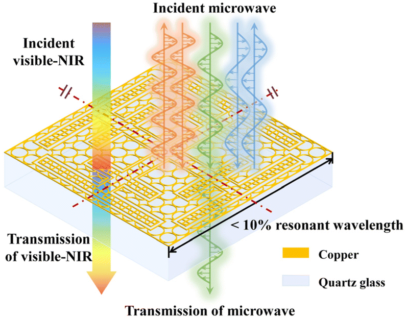
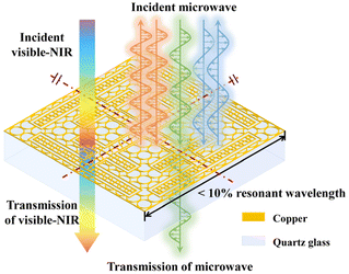
The structure of MMFSMs is shown in Fig. 1; copper-based frequency-selective metasurfaces (FSMs) are a two-dimensional periodic array on a quartz glass substrate. The dielectric constant of quartz glass is 3.75, and the thickness of copper and quartz glass is 300 nm and 500 μm, respectively. The quartz glass substrate is optically transparent from the visible to near-infrared band; owing to the low metal duty cycle, the MMFSM can achieve optical transparency in the same band, and the transparent band can be expanded if another substrate material is chosen. In the microwave band, the MMFSM is frequency selective, transmitting only at the demand frequency while cutting off at the non-demanding frequency. Furthermore, the unit cell period of the MMFSM needs to be less than 10% wavelength at the resonant frequency and its structure should show a four-fold symmetry for excellent oblique incidence stability and polarization insensitivity.
 |
| | Fig. 1 Schematic of the MMFSM. | |
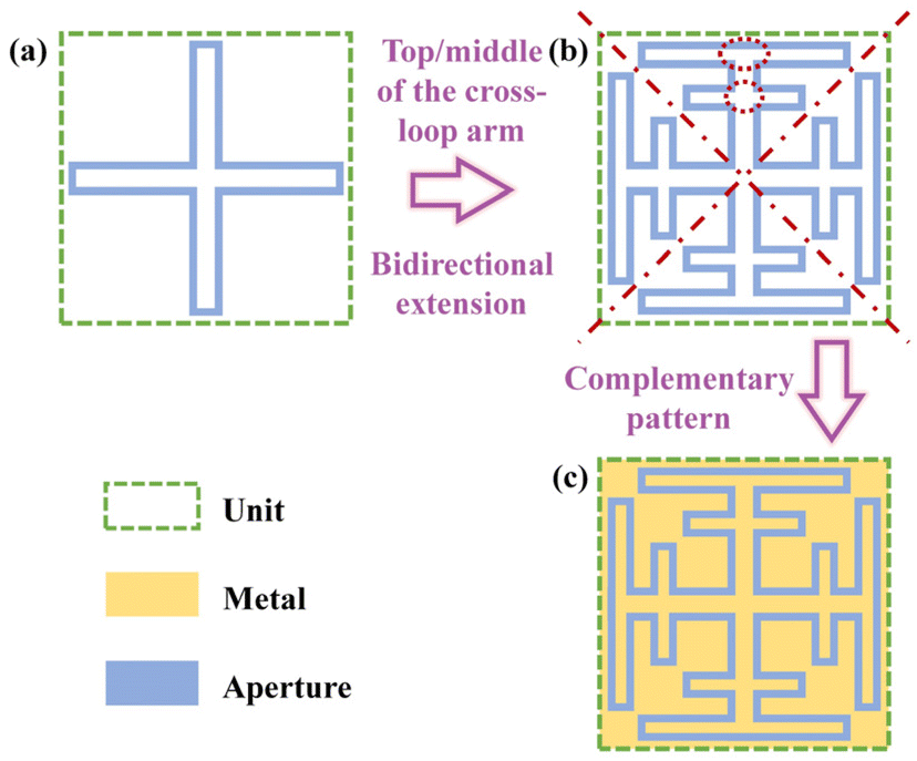
The period of the FSS based on the convoluted structure is smaller than that of the conventional FSS; however, those structures do not usually show a four-fold symmetry, which leads to FSS polarization sensitivity. The loop-apertures have a smaller unit period than that of other conventional apertures; based on this, the cross-loop aperture (Fig. 2(a)) has a four-fold symmetry and suitable to be the original structure for the symmetry-convoluted miniaturization method used in this work. The miniaturization process schematic is shown in Fig. 2, where the top and middle of the cross-loop arms bidirectionally extend to close to the diagonal of the unit cell. The complementary pattern of the miniaturized cross-loop aperture is the unit cell of the MFSM (Fig. 2(c)). The effective length of the aperture per unit is extended, which brings a lower resonant frequency under the same unit period. This means a smaller period can be achieved at the same resonant frequency. To verify this point, we adjusted the periods of the CLFSS and MFSM to achieve the same resonant frequency of 16.5 GHz. The periods of the MFSM and CLFSS are 1450 μm and 3800 μm, respectively, corresponding to 7.98% λ and 21.09% λ, where λ is the wavelength at the resonant frequency. After miniaturization, there is a 62.16% reduction in the period.
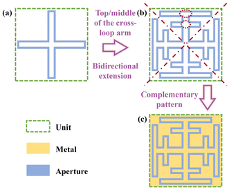 |
| | Fig. 2 Schematic of the miniaturization process based on CAFSS: (a) cross-loop aperture, (b) miniaturized cross-loop aperture, and (c) unit cell of MFSMs. | |
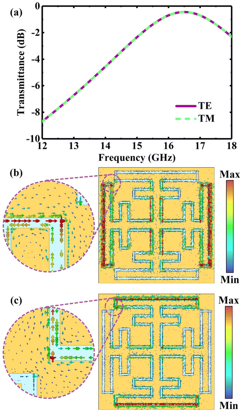
The simulated transmittance of the MFSM in the Ku band (12–18 GHz) at normal incidence is shown in Fig. 3(a); the resonant frequency, passband loss and 3 dB bandwidth is 16.50 GHz, 0.45 dB and 4.04 GHz, respectively. The transmittance under TE polarization almost overlaps with that under TM polarization, illustrating that the transmission of the MFSM is polarization insensitive at normal incidence. To further analyse the mechanism of miniaturization, the surface current densities of the MFSM for the resonant frequency (16.5 GHz) at normal incidence under TE and TM polarization are simulated and shown in Fig. 3(b) and (c). The surface current passes through the entire miniaturized cross-loop aperture, especially at the top extension arms, indicating that the length of the aperture is effectively extended within the unit period. Moreover, the current density is primarily concentrated at the left and right sides under TE polarization and at the top and bottom sides under TM polarization. Because the MFSM is four-fold symmetric, and the surface current density distributions under TE polarization corresponding to the x-axis and those under TM polarization corresponding to the y-axis are similar. This proves again that the MFSM is polarization insensitive at normal incidence.
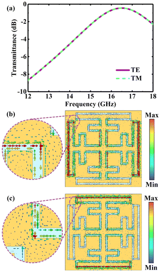 |
| | Fig. 3 (a) Simulated transmittance of the MFSM in the Ku band (12–18 GHz) at normal incidence under TE and TM polarization. (b and c) Simulated surface current density of the MFSM at its resonant frequency (16.5 GHz) under (a) TE polarization and (b) TM polarization. Insets in (b) and (c) are the amplified surface current density of the corresponding purple dotted circle regions. | |
2.2 Design of MMFSMs
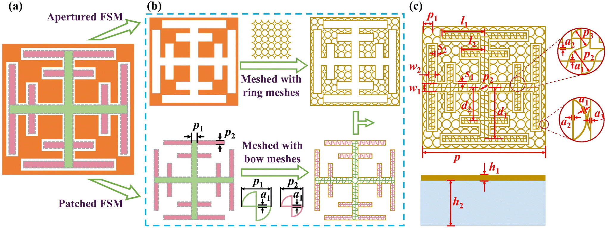
The designed MFSM possesses the characteristic of miniaturization, low passband loss and polarization insensitivity, but it has poor optical transparency. Therefore, the MFSM needs to be transparent to be available on the optical window. The transparent method utilized in this work is the mesh method shown in Fig. 4(a), and MFSMs can be divided into apertured FSMs and patched FSMs. The pattern of the patched FSM is simple and uniformly dispersed, whereas that of the apertured FSM is more complex. According to Fig. 3, the surface current density is more concentrated in the patched FSM than in the apertured FSM, and hence, the metallic mesh used for the meshed patched FSM needs a higher conductivity. Due to the differences in the pattern feature and metallic mesh conductivity requirements, if the patched FSM and apertured FSM are meshed with the same mesh structure, the optical transmission will cause an unnecessary decrease; consequently, different metallic meshes are used for meshed process. In addition, because the current density is primarily concentrated at the aperture parts, it is necessary to retain the metallic wires at the edge part of the aperture to maintain the edge shape features, which can prevent frequency selection characteristics from changing after the meshing of FSMs. As shown in Fig. 4, the apertured FSM is meshed with ring meshes featuring a larger aperture, whereas the patched FSS with a higher conductivity requirement is meshed with completely mixed bow meshes with an array of two structural parameters. The unit periods of the bow mesh are determined by the widths of the extension arm and cross-loop arm in the patched FSS. The overlapping area at the centre of the unit is replaced by a metallic ring. Combining the meshed apertured FSS and patched FSS, the unit cell layout of the MMFSM is depicted in Fig. 4(c). To ensure that the bow meshes are completely mixed, the length and width of the extension arms are optimized, and the structural parameters after co-design are the widths of cross-loop arms and extension arms are w1 = 100 μm and w2 = 75 μm, respectively. The lengths of the long and short extension arms are l1 = 500 μm and l2 = 275 μm, respectively. The distances between the center point of the long and short extension arms from the center point of the unit cell are d1 = 612.5 μm and d2 = 397.5 μm, respectively. The widths of the gap formed by the patched FSS and apertured FSS are s1 = 20 μm (parallel to the original cross-loop arms) and s2 = 30 μm (perpendicular to the original cross-loop arms) respectively. To ensure good optical transmittance, the line-width of meshes is a1 = 3.5 μm, the period of the ring meshes is p1 = 110 μm, and the periods of the bow meshes used in cross parts and extension arm parts are p2 = 100 μm and p3 = 75 μm, respectively. To ensure the frequency selection characteristics of the FSM, the width of metallic wires at the aperture edge part is a2 = 5 μm. The period of the unit cell is p = 1450 μm. After meshing, the optical transmission of the MMFSM improved from 20.7% (MFSM) to 85.9%, resulting in a decline of 82.2% in optical transmittance loss.
 |
| | Fig. 4 Schematic of the mesh process of the MFSM. (a) Schematic of the structure of the MFSM; the orange part denotes the apertured FSM, and green and pink parts denote the patched FSM. (b) Schematics of the specific meshed process of the apertured FSM and patched FSM. (c) Unit cell layout of the MMFSM. The dimensions are w1 = 100 μm, w2 = 75 μm, l1 = 500 μm, l2 = 275 μm, d1 = 612.5 μm, d2 = 397.5 μm, s1 = 20 μm, s2 = 30 μm, a1 = 3.5 μm, p1 = 110 μm, p2 = 100 μm, p3 = 75 μm, a2 = 5 μm, p = 1450 μm, h1 = 0.3 μm, h2 = 500 μm. | |
2.3 Diffraction distribution analysis
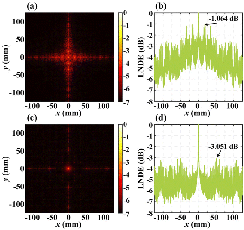
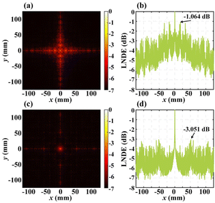
The application of FSMs to the optical window requires not only broadband optical transparency, but also a minimal impact on the imaging quality. Actually, in imaging and observation, the high-order diffraction concentration may cause deceptive targets, and hence, minimizing the maximum high-order diffraction energy can improve the image quality. To analysis the image quality before and after the mesh process, we used the Fourier transform model to evaluate the diffraction distributions and normalized diffraction energy for the MFSM and MMFSM under vertical irradiation. In simulation, the optical wavelength is 632.8 nm and the diffraction distributions shown in Fig. 5(a)–(c) are obtained 3-metre away from the FSM. Owing to the small normalized diffraction energy shown in Fig. 5(b)–(d), the logarithm coordinate is employed for vertical coordinates to enable a clearer visualization of the normalized high-order diffraction energy (NHDE). In Fig. 5(a), the high-order diffraction of MFSM is primarily distributed on the cross axes, with obvious concentration points on each axis, resulting in poor imaging quality; however, after the MFSM is meshed (MMFSM), the high-order diffraction is obviously homogenized (Fig. 5(c)) and uniformly distributed within a circle of 25 mm radius from the zero-order spot, and although it is slightly concentrated on the cross-axis in the range of 25–100 mm from the zero-order spot, the diffraction energy is much lower than that of the MSFM. As shown in Fig. 5(b) and (d), a quantitative comparison between the NHDE of the MFSM and MMFSM reveals that the maximum NHDE of MMFSM is only −3.051 dB (0.089%), representing a 98.97% decrease compared to −1.064 dB (8.630%) of the MFSM. Both the diffraction distribution analysis and quantitative NHDE decline demonstrate that the MMFSM effectively homogenizes the high-order diffraction. Due to the high optical transparency and uniform high-order diffraction distribution, the MMFSM is suitable for optical window applications.
 |
| | Fig. 5 Simulation results of diffraction distribution and normalized diffraction energy results for (a and b) MFSM and (c and d) MMFSM. | |
2.4 Microwave transmission analysis
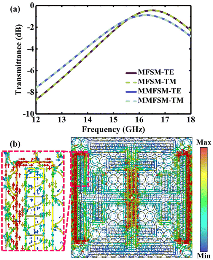
Microwave transmission is one of the most crucial properties of the MMFSM. Fig. 6(a) shows the simulated transmission of the MMFSM and MFSM in the Ku band at normal incidence. Compared with the MFSM, the MMFSM has a slightly lower passband frequency (16.268 GHz) and a broader 3 dB bandwidth (4.58 GHz), and the density of the MMFSM at its resonant frequency under TE polarization is shown in Fig. 6(b). The current density not only concentrates at the apertures, but also extends along the metallic mesh edge, extending the effective length of the aperture per unit, thus red-shifting the resonant frequency. Although the conductivity of metallic mesh is stronger than that of other TCMs, it is still lower than that of the pure metal, which leads to a slight increase in the passband loss.
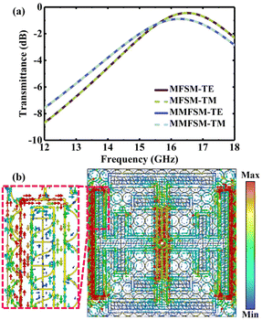 |
| | Fig. 6 (a) Comparison of the simulated transmittance for the MFSM and MMFSM under different polarizations. (b) Simulated surface current density of the MMFSM at its resonant frequency under TE polarization. Inset in (b) is the locally amplified surface current density of the red dotted box region. | |
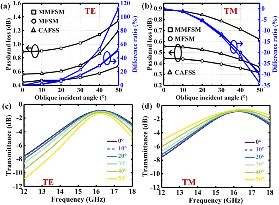
An important application of miniaturization is the oblique incidence stability of frequency selection characteristics; consequently, the transmission characteristics of the CAFSS, MFSM and MMFSM at different incidence angles under both TE and TM polarizations were simulated and analysed. The passband losses at the resonant frequency versus incidence angle are shown in Fig. 7(a) and (b), and the resonant frequency refers to the frequency with the minimum passband loss in the Ku band under normal incidence and is the demand frequency for practical applications. As the passband losses among various structures under normal incidence are not uniform, the difference ratio Rd is expressed for convenient comparison as follows:
| |  | (1) |
where
Rd is the difference ratio,
θ is the incidence angle,
TPL|θ=0 is the passband loss at resonant frequency under normal incidence, and
TPL|θ is the passband loss at the resonant frequency at the incidence angle
θ. As shown in
Fig. 7, the passband losses gradually increase with the increase in incidence angle under TE polarization. When the oblique incidence angle is less than 20°, the CAFSS, MFSM, and MMFSM demonstrate similar difference ratios, indicating that miniaturization has a negligible impact on the stability at small oblique incidence angles; however, as the oblique incidence angle increases beyond 20°, the difference ratio of CAFSS gradually surpasses that of the MFSM and MMFSM and even exceeds double the value (113.46%) compared to that of the MFSM (52.74%) under 50° oblique incidence angle, proving that miniaturization is more stable at large oblique incidence angles. Under TM polarization, the passband loss decreases as the incidence angle increases, and the difference ratio for the three structures is similar (∼30%@50°). Consequently, the main advantage of miniaturization is TE polarization.
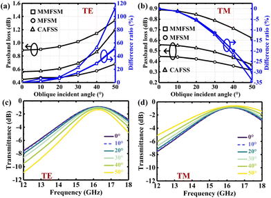 |
| | Fig. 7 (a)–(b) Passband loss and difference ratio versus incidence angle of CAFSS, MFSM, and MMFSM under (a) TE polarization and (b) TM polarization. (c)–(d) Simulated transmittance of the MMFSM for different incidence angles under (c) TE polarization and (d) TM polarization. | |
The simulated transmittance of the MMFSM under TE and TM polarizations at different incidence angles is shown in Fig. 7(c) and (d), respectively. The transmittance at normal incidence is essentially the same for both polarizations (passband loss ∼0.89 dB; 3 dB bandwidth ∼4.58 GHz). However, as the incidence angle increases, the passband loss of the MMFSM increases (1.35 dB@50°) and the 3 dB bandwidth decreases (3.14 GHz@50°) under TE polarization; in contrast, the passband loss of the MMFSM decreases (0.62 dB@50°) and the 3 dB bandwidth increases (6.52 GHz@50°) under TM polarization.
3 Results and discussion, experimental
3.1 Fabrication of MFSM and MMFSM samples
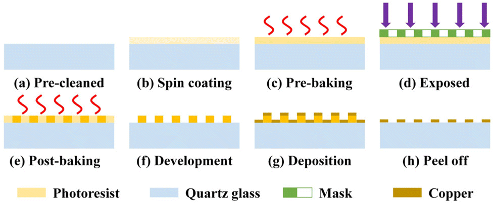
To verify and compare the optical and microwave characteristics of the designed FSMs, MFSM and MMFSM samples were fabricated via a lift-off process with thermal evaporation technique; the fabrication process is shown in Fig. 8. First, the surface of the quartz glass substrate (6.5 × 6.5 mm2) was pre-cleaned with alcohol and acetone, and after cleaning with pure water, a 1.2 μm-thick layer of AR4400-05 photoresist was spin-coated onto the substrate surface and subjected to pre-baking. The photoresist of the complementary part of the FSM pattern was exposed using vacuum contact lithography and a pre-prepared chromium mask. By controlling the temperature and duration time of post-baking, it was ensured that the exposed photoresist undergoes sufficient cross-linking reactions. Only the photoresist complementary to the FSM pattern remains on the substrate after development. Next, a 400 nm-thick copper film was deposited onto the prototype and substrate using a thermal evaporation technique. Subsequently, the remaining photoresist was removed using a remover, while the unneeded copper deposited on the photoresist was peeled off. Finally, the FSM samples were obtained after cleaning.
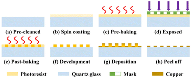 |
| | Fig. 8 Fabrication process of the FSM sample: (a) pre-cleaning; (b) spin coating; (c) pre-baking; (d) exposure; (e) post-baking; (f) development; (g) deposition; (h) peeling off. | |
3.2 Measured optical transmittance and diffraction distribution
Fig. 9(a) is the measured normalized optical transmittance of MFSM and MMFSM samples. In the visible to near-infrared band, the average normalized optical transmittance of the MFSM sample before the mesh process is only 20.6%, whereas that of the MMFSM sample after the mesh process reaches 87.2%; the meshed process brings an 83.9% decrease in the optical transmittance loss. Fig. 9(b) and (c) show the far-field diffraction distribution experimental images of the fabricated MFSM and MMFSM samples, respectively, which are consistent with the simulated results presented in Fig. 5(a)–(c). The high-order diffraction of the MFSM is primarily concentrated on the cross axes, whereas that of the MMFSM is uniformly distributed in the center with some concentrated on the cross axes besides the center. However, the diffraction energy of the MMFSM is significantly lower than that of the MFSM. It is demonstrated that the MMFSM exhibits a more uniform high-order diffraction distribution and is suitable for optical window applications.
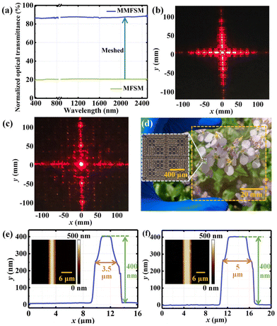 |
| | Fig. 9 Comparison of the optical properties of the MFSM and MMFSM samples and the characterization of MMFSM samples: (a) normalized optical transmittance of the MFSM and MMFSM samples; far-field diffraction distribution experimental images of the fabricated (b) MFSM and (c) MMFSM samples; (d) photograph of the fabricated MMFSM sample (insets in (d) are the micrographs of the MMFSM sample); and height profiles of metal wires of mesh parts (e) and aperture edge parts (f) in the MMFSM sample (insets in (e) and (f) are the corresponding AFM images). | |
The MMFSM sample maintains more than 85.8% optical transmission in the range of 380–2500 nm. The average optical transmission in the visible and near-infrared bands is 86.33% and 87.35%, respectively. Fig. 9(d) show the photograph of the MMFSM sample, with flowers clearly visible behind it, proving that the MMFSM sample exhibits high optical transparency. The insets in Fig. 9(d) are the micrographs of the MMFSM sample, which are consistent with the design structure. To measure the real linewidth and thickness of the sample, metal wires in mesh parts as well as aperture edge parts were characterized by atomic force microscopy (AFM), as shown in Fig. 9(e) and (f); the insets are the corresponding AFM images. The results indicate that the linewidths of the metal wires are 3.5 μm and 5 μm, respectively, which are in accordance with the design parameters. Additionally, both thicknesses are 400 nm, ensuring the strong conductivity of metal wires.
3.3 Measured microwave transmittance
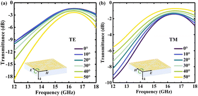
We also used a vector network analyzer combined with a Ku-band antenna to measure the transmission of the MMFSM sample under various polarizations and incidence angles. As shown in Fig. 10, under TE polarization, the passband loss of the MMFSM sample gradually increases and the 3 dB bandwidth gradually decreases as the incidence angle increases, whereas under TM polarization, the change trends of passband loss and 3 dB bandwidth are exactly opposite to those of TE polarization, which are consistent with the simulation trend. The transmission of the MMFSM sample under TE and TM polarization at normal incidence is almost uniform, with a passband loss of only 1.44 dB (16.4 GHz) and a 3 dB bandwidth of 4.62 GHz, experimentally demonstrating that the MMFSM sample is polarization insensitive. Even when the oblique incidence angle increases up to 50°, the passband loss at 16.4 GHz remains less than 2.38 dB under TE polarization, whereas it declines to 0.74 dB under TM polarization, proving that the proposed MMFSM has a stable frequency response with the oblique incidence angle up to 50°.
 |
| | Fig. 10 The measured transmittance of the MMFSM for various incidence angles under (a) TE polarization and (b) TM polarization. | |
Table 1 compares the MMFSM to the previously reported optically transparent FSS in terms of visible transmittance, near-infrared transmittance, relative unit period, passband loss, and angle stability. Although the visible transmittance of the MMFSM is comparable to that of other FSSs, it has the smallest relative cell period, minimum passband loss and maximum angle stability. Furthermore, there is rarely infrared transparent FSS yet; however, the MMFSM can achieve 87.35% transmission in the near-infrared band.
Table 1 Comparison of the MMFSM with the previous optically transparent FSS
| Ref. |
Visible transmittance (%) |
Near infrared transmittance (%) |
Relative unit period (% λa) |
Passband loss (dB) |
Angle stability (°) |
|
Wavelength at the resonant frequency of the frequency selective surface.
|
|
65
|
76.2 |
N/A |
20.00 |
N/A |
30 |
|
58
|
90.31 |
N/A |
11.87 |
−3.269 |
N/A |
|
63
|
87.5 |
N/A |
21.20 |
−2.00 |
N/A |
| This work |
86.33 |
87.35 |
7.86 |
−1.44 |
50 |
4 Conclusions
In summary, a meshed miniaturized frequency-selective metasurface with stable microwave transmission characteristics, low passband loss, and good optical imaging quality was proposed and fabricated in this work. The measurement results of the MMFSM indicated that the broadband average optical transmittance from the visible to near-infrared band reached 87.2%, and the passband loss was 1.446 dB. The fabricated MMFSM sample also has great oblique incidence stability (only 2.38 dB passband loss at 50° oblique incidence) and polarization insensitivity. In addition, the MMFSM has a uniform high-order diffraction distribution. We believe that our MMFSM has great application potential in the optical and microwave communication field.
Author contributions
Yilei Zhang: Conceptualization, investigation, methodology, writing-original draft. Bowen Zhang: Data curation, visualization, software. Zhengang Lu: Conceptualization, funding acquisition, validation, writing – review & editing. Heyan Wang: Formal analysis, methodology, supervision. Lin Han: Resources, investigation. Jiubin Tan: Project administration, supervision.
Conflicts of interest
There are no conflicts to declare.
Acknowledgements
This study was financially supported by the National Natural Science Foundation of China (NSFC) (Grant No. 61975046).
References
- Y. Li, Q. Zhang, Y. Hong and J. Yin, Adv. Funct. Mater., 2021, 31, 2105641 CrossRef CAS.
- C. Ma, Y. Chang, S. Wu and R. R. Zhao, ACS Appl. Mater. Interfaces, 2022, 14, 33892–33902 CrossRef CAS PubMed.
- R. Su, J. Chen, X. Zhang, W. Wang, Y. Li, R. He and D. Fang, Small, 2023, 19, 2206391 CrossRef CAS PubMed.
- P. Dawar, N. S. Raghava and A. De, Front. Inf. Technol. Electron. Eng., 2018, 18, 1883–1891 CrossRef.
- H.-H. Hsiao, C. H. Chu and D. P. Tsai, Small Methods, 2017, 1, 1600064 CrossRef.
- J. Kim, J. Seong, Y. Yang, S.-W. Moon, T. Badloe and J. Rho, Adv. Photonics, 2022, 4, 024001 CAS.
- M. Y. Shalaginov, S. An, Y. Zhang, F. Yang, P. Su, V. Liberman, J. B. Chou, C. M. Roberts, M. Kang, C. Rios, Q. Du, C. Fowler, A. Agarwal, K. A. Richardson, C. Rivero-Baleine, H. Zhang, J. Hu and T. Gu, Nat. Commun., 2021, 12, 1225 CrossRef CAS PubMed.
- J. Yang, S. Gurung, S. Bej, P. Ni and H. Lee, Rep. Prog. Phys., 2022, 85, 036101 CrossRef PubMed.
- Z. X. Wang, H. Yang, R. Shao, J. W. Wu, G. Liu, F. Zhai, Q. Cheng and T. J. Cui, Engineering, 2022, 17, 64–74 CrossRef.
- I. Fernandez-Corbaton, R. Griesmaier, M. Knöller and C. Rockstuhl, J. Comput. Phys., 2023, 475, 111854 CrossRef CAS.
- Z. Lu, Y. Liu, Y. Zhang, H. Wang and J. Tan, Adv. Mater. Technol., 2023, 8, 2202081 CrossRef CAS.
- X. Yuan, H. Zhou, X. Ye, R. Zhang, M. Chen, X. Zhang, W. Li, X. Chen, L. Li, Y. Huang, G. Wang and D. Fang, IEEE Trans. Antennas Propag., 2022, 70, 3489–3494 Search PubMed.
- J. Zhang, L. Shao, Z. Li, C. Zhang and W. Zhu, ACS Appl. Mater. Interfaces, 2022, 14, 31075–31084 CrossRef CAS PubMed.
- X. Wan, C. Xiao, H. Huang, Q. Xiao, W. Xu, Y. Li, J. Eisenbeis, J. Wang, Z. Huang, Q. Cheng, S. Jin, T. Zwick and T. Cui, Engineering, 2022, 8, 86–95 CrossRef.
- R.-y. Wu and T.-j. Cui, Front. Inf. Technol. Electron. Eng., 2020, 21, 4–26 CrossRef.
- Z. Tian, C. Shen, J. Li, E. Reit, Y. Gu, H. Fu, S. A. Cummer and T. J. Huang, Adv. Funct. Mater., 2019, 29, 1808489 CrossRef PubMed.
- H. Xue, Y. Yang, F. Gao, Y. Chong and B. Zhang, Nat. Mater., 2019, 18, 108–112 CrossRef CAS PubMed.
- Y. Zhou, J. Chen, L. Liu, Z. Fan and Y. Ma, NPG Asia
Mater., 2020, 12, 27 CrossRef.
- M. Gulzari and C. W. Lim, Arch. Comput. Methods Eng., 2021, 29, 1137–1198 Search PubMed.
- A. L. Chen, Y.-S. Wang, Y.-F. Wang, H.-T. Zhou and S.-M. Yuan, Appl. Mech. Rev., 2022, 74, 020801 CrossRef.
- L. Cao, Y. Zhu, S. Wan, Y. Zeng and B. Assouar, Int. J. Eng. Sci., 2022, 181, 103768 CrossRef.
- H.-W. Dong, S.-D. Zhao, M. Oudich, C. Shen, C. Zhang, L. Cheng, Y.-S. Wang and D. Fang, Phys. Rev. Appl., 2022, 17, 044013 CrossRef CAS.
- E. J. P. Miranda, E. D. Nobrega, A. H. R. Ferreira and J. M. C. Dos Santos, Mech. Syst. Signal Process., 2019, 116, 480–504 CrossRef.
- Q. Lu, X. Li, X. Zhang, M. Lu and Y. Chen, Engineering, 2022, 17, 22–30 CrossRef.
- H. Chen, H. Chen, X. Xiu, Q. Xue and W. Che, IEEE Antennas Wirel. Propag. Lett., 2021, 20, 2319–2323 Search PubMed.
- M. I. Hossain, N. Nguyen-Trong, K. H. Sayidmarie and A. M. Abbosh, IEEE Trans. Antennas Propag., 2020, 68, 8215–8220 Search PubMed.
- Y. Li, S.-W. Wong, S. Wang, J.-Y. Lin, B. Liu, L. Zhu and Y. He, IEEE Antennas Wirel. Propag. Lett., 2021, 20, 13–17 Search PubMed.
- H. Wakatsuchi, J. Long and D. F. Sievenpiper, Adv. Funct. Mater., 2019, 29, 1806386 CrossRef.
- Y. Youn, D. Kim, S. Chang, J. Choi and W. Hong, IEEE Trans. Antennas Propag., 2022, 70, 12387–12392 Search PubMed.
- S. Genovesi, F. Costa and A. Monorchio, IEEE Trans. Antennas Propag., 2012, 60, 2327–2335 Search PubMed.
- T. Hong, S. Guo, W. Jiang and S. Gong, IEEE Trans. Antennas Propag., 2022, 70, 3459–3468 Search PubMed.
- D. J. Kern, D. H. Werner, A. Monorchio, L. Lanuzza and M. J. Wilhelm, IEEE Trans. Antennas Propag., 2005, 53, 8–17 Search PubMed.
- M. Raspopoulos and S. Stavrou, IEEE Trans. Antennas Propag., 2011, 59, 2998–3005 Search PubMed.
- B.-Q. Lin, S.-h. Zhao, X.-y. Da, Y.-w. Fang, J.-j. Ma and Z.-H. Zhu, Microw. Opt. Technol. Lett., 2015, 57, 2572–2576 CrossRef.
- B.-q. Lin, S.-h. Zhou, X.-y. Da, Y.-w. Fang, Y.-j. Li and W. Li, Electron. Lett., 2015, 51, 883–884 CrossRef.
- W. Yin, H. Zhang, T. Zhong and X. Min, IEEE Trans. Electromagn. Compat., 2019, 61, 1234–1238 Search PubMed.
- C. Cheng-Nan and C. Keng-Ping, IEEE Antennas Wirel. Propag. Lett., 2009, 8, 1175–1177 Search PubMed.
- M. Yan, S. Qu, J. Wang, J. Zhang, A. Zhang, S. Xia and W. Wang, IEEE Antennas Wirel. Propag. Lett., 2014, 13, 639–641 Search PubMed.
- G. Yang, T. Zhang, W. Li and Q. Wu, IEEE Antennas Wirel. Propag. Lett., 2010, 9, 1018–1021 Search PubMed.
- M. Hussein, J. Zhou, Y. Huang and B. Al-Juboori, IEEE Antennas Wirel. Propag. Lett., 2017, 16, 2791 Search PubMed.
- H. Li, C. Yang, Q. Cao and Y. Wang, IEEE Antennas Wirel. Propag. Lett., 2017, 16, 341–344 Search PubMed.
- N. P. Lawrence, C. Fumeaux and D. Abbott, Microw. Opt. Technol. Lett., 2017, 59, 2479–2484 CrossRef.
- B. Li and R. Ne, Int. J. Electron. Commun., 2021, 130, 153580 CrossRef.
- y. Z. j. C. z. L. h. W. j. Tan, Front. Inf. Technol. Electron. Eng., 2021, 22, 1532–1540 CrossRef.
- Z. Lu, Y. Zhang, X. Lu, H. Wang and J. Tan, Opt. Laser Technol., 2021, 144, 107396 CrossRef CAS.
- Z. Lu, Y. Zhang, H. Wang, C. Xia, Y. Liu, S. Dou, Y. Li and J. Tan, Engineering, 2023, 29, 198–206 Search PubMed.
- K. Xue, H. Zhai, S. Li and Y. Shang, IEEE Antennas Wirel. Propag. Lett., 2020, 19, 24–28 Search PubMed.
- R. Martinez-Lopez, J. Rodriguez-Cuevas, A. E. Martynyuk and J. I. Martinez-Lopez, IEEE Trans. Antennas Propag., 2020, 68, 4668–4676 Search PubMed.
- Q. Chen, J. Bai, L. Chen and Y. Fu, IEEE Antennas Wirel. Propag. Lett., 2015, 14, 80–83 Search PubMed.
- Q. Chen, D. Sang, M. Guo and Y. Fu, IEEE Trans. Antennas Propag., 2019, 67, 1045–1052 Search PubMed.
- H. Liu, K. L. Ford and R. J. Langley, Electron. Lett., 2008, 44, 1054 CrossRef.
- A. Mathivanan and P. Saravanan, Microw. Opt. Technol. Lett., 2022, 64, 1991–1999 CrossRef.
- B. Hua, X. He and Y. Yang, Electron. Lett., 2017, 53, 1502–1504 CrossRef.
- Y. Li, G. Han, G. Cao, X. Zhang and Z. Zhang, J. Electromagn. Waves Appl., 2021, 36, 1212–1228 CrossRef.
- S. S. Sampath, R. Sivasamy and K. J. J. Kumar, IEEE Trans. Electromagn. Compat., 2019, 61, 1678–1681 Search PubMed.
- T. Hong, K. Peng and M. Wang, IEEE Antennas Wirel. Propag. Lett., 2019, 18, 2026–2030 Search PubMed.
- N. Liu, X. Sheng, C. Zhang, J. Fan and D. Guo, IEEE Antennas Wirel. Propag. Lett., 2017, 16, 2384–2387 Search PubMed.
- X. Lu, Y. Liu, Z. Lu, Y. Zhang, H. Wang, R. Ji and J. Tan, Opt. Lett., 2019, 44, 1253–1256 CrossRef CAS PubMed.
- J. Liang, Q. Cao, Y. Wang and Z. Wan, IEEE Antennas Wirel. Propag. Lett., 2021, 20, 2549–2553 Search PubMed.
-
Z. Lu, Y. Han, W. Zhang and B. Li, Presented in part at the 2020 International Conference on Microwave and Millimeter Wave Technology (ICMMT), 2020.
- C. Tsakonas, S. C. Liew, C. Mias, D. C. Koutsogeorgis, R. M. Ranson, W. M. Cranton and M. Dudhia, Electron. Lett., 2001, 37, 1464–1466 CrossRef.
- J. Li, L. Shi, H. Chen, L. Qu, Y. Yi, Q. Zhang, S. Fu, Y. Ma and J. Wang, Opt. Commun., 2023, 536, 129365 CrossRef CAS.
- Y. Han, Y. M. Liu, P. Jin, B. Liu, J. Ma and J. B. Tan, Electron. Lett., 2014, 50, 381–383 CrossRef.
- Y. Liu and J. Tan, Opt. Express, 2013, 21, 4228–4234 CrossRef PubMed.
- S. K. Sharma, D. Zhou, A. Luttgen and C. D. Sarris, IEEE Antennas Wirel. Propag. Lett., 2019, 18, 202–206 Search PubMed.
|
| This journal is © The Royal Society of Chemistry 2024 |
Click here to see how this site uses Cookies. View our privacy policy here. 
 *abc,
Heyan
Wang
bc,
Lin
Han
bc and
Jiubin
Tan
bc
*abc,
Heyan
Wang
bc,
Lin
Han
bc and
Jiubin
Tan
bc