
Aberrant photoelectric effect in the topological insulator/n-GaN heterojunction (Bi2Te3/n-GaN) under unpolarized illumination†
Faizan
Ahmad
a,
Kavindra
Kandpal
 b,
Roshani
Singh
c,
Rachana
Kumar
d and
Pramod
Kumar
*c
b,
Roshani
Singh
c,
Rachana
Kumar
d and
Pramod
Kumar
*c
aElectrical, Computer and Energy Engineering, Arizona State University, Tempe, AZ-85281, USA. E-mail: faizanash1986@gmail.com
bDepartment of Electronics and Communication Engineering, IIIT-Allahabad, Prayagraj, 211012, India
cSpintronics and Magnetic Materials Laboratory, Department of Applied Sciences, IIIT-Allahabad, Prayagraj, 211012, India. E-mail: pkumar@iiita.ac.in
dASSIST Division, CSIR-Indian Institute of Toxicology Research, Lucknow, Uttar Pradesh 226024, India
First published on 5th December 2023
Abstract
A topological insulator has a unique graphene-like Dirac cone conducting surface state, which is excellent for broadband absorption and photodetector applications. Experimental investigations on the Bi2Te3/n-GaN heterojunction exhibited an aberrant photoelectric effect under the influence of unpolarized light. Transport measurements of the Bi2Te3/n-GaN heterojunction revealed a negative photoconductance, with a sudden increase in resistance. This was consistent with the applied range of wavelength and power used for incident light while it was contrary to the usual gap-state transition model, which states that a negative conductance is due to the trapping of charge carriers. The observed aberrant photoelectric effect seen in Bi2Te3/n-GaN heterojunction devices was due to the polycrystalline nature of the Bi2Te3 topological insulator film, where the incident photon-induced bandgap in the Dirac cone surface state resulted in a negative photoelectric effect. This phenomenon opens the possibility for applications in highly sensitive photodetectors and non-volatile memories, along with employing the bandgap-opening concept in retinomorphic devices.
1. Introduction
Gallium nitride (GaN) as a semiconductor (SC) compound has been extensively used in electronics and optoelectronic applications.1 It is the wide and direct bandgap SC that is mostly employed in ultraviolet (UV) detectors.2,3 Its bandgap tunability from the infrared (0.8) to the ultraviolet (6.1 eV) makes this material fascinating for researchers.4–6 Devices involving different quantum confinement levels are also being realized with GaN, such as single-photon emitters and other nanophotonic devices.7,8 However, GaN-based photodetectors have limitations due to the defects and low conductivity of the material. Considering the low charge carrier mobility and the short carrier lifetime, the photosensitive area of the GaN photodiode is restricted to ∼0.1 mm2, which makes it less effective.9–11 The search for a more effective GaN-based photodiode for overcoming these limitations is thus imperative. The major efforts at this are aimed toward creating more efficient and multifunctional devices by growing another material on GaN.12,13 Ferromagnetic doping and the growth of other functional materials have also been realized with GaN14 to work in this direction. Topological insulators (TIs) are a fascinating class of materials due to their exotic gapless surface states and bulk bandgap. Their surface states make them unique materials,15 which are well protected from backscattering. Bismuth telluride (Bi2Te3), bismuth selenide (Bi2Se3), and antimony telluride (Sb2Se3) are some well-known three-dimensional (3D) TI materials, possessing a single Dirac cone on their surfaces.15 High-quality Bi2Se3, Bi2Te3, and Sb2Te3 TI films have been fabricated by employing various methods, e.g. physical vapour deposition (PVD) and chemical vapour deposition (CVD) techniques on sapphire,16 SrTiO3,17 Si,18 and GaN19 substrates. These differently grown TI film heterostructures with their unique properties find applications in spintronic devices, quantum computing, ultrafast transistors, and low-power electronic devices. Recent work in TIs is being focused on their optical study with the excellent response of their surface states to light. An enhanced performance with broadband photodetection from the infrared to the terahertz20 has been observed in TIs due to their Dirac surface states. The warping effect-induced optical absorption and the enhanced signal-to-noise ratio (SNR) in TIs makes them analogous to graphene in photodetector applications.21 Bi2Te3 is one of the interesting topological insulators22 as a narrow bandgap (0.17 eV)23 semiconductor, and an excellent thermoelectric material at room temperature.24 Further, the polycrystalline Bi2Te3 TI film has recently been observed with multifunctional properties that are interesting for photodetection.25 However, the Bi2Te3/n-GaN heterojunction has also been recognized as a good photovoltaic for mid-infrared detectors26 and its charge carrier dynamics is favourable for optoelectronics device applications.27 Therefore, Bi2Te3 and GaN seem to be appealing choices of materials for realizing heterojunctions for photodetector applications.We grew multiple Bi2Te3/n-GaN heterojunctions, with a polycrystalline TI thin film on a GaN template (on sapphire). We observed an aberrant photoelectric effect in our heterojunction devices under illumination with unpolarized light. This unconventional effect, involving the negative photoconductance (NPC) phenomenon,28,29 resulted in a reduction of the conductivity. Our results are contrary to the usual positive photoconductance (PPC) effect, where the conductivity increases with illumination. This NPC effect has been detected earlier in bulk semiconductors28,29 and in low-dimensional structures.30–33 However, defying all the previous explanations regarding NPC, the present aberrant effect in our heterojunction was due to the Dirac bandgap opening at the surface of the Bi2Te3 TI film. Further, this aberrant effect was found to be consistent for a range of optical wavelengths and powers of the incident unpolarized light. This study provides an important insight into the optical and transport study of TI-based heterojunctions for highly sensitive photodetector applications.34,35
2. Experimental details
An n-GaN template (thickness: 3.5 μm) on c-plane sapphire (thickness: 0.333 mm) was used as a substrate to make Bi2Te3/n-GaN heterojunctions. The carrier concentration in the n-GaN template was 1.9 × 1018 cm−3. The substrate was prior ultrasonically cleaned with acetone, isopropanol, and de-ionized (DI) water for 10 min. A solution of HCl![[thin space (1/6-em)]](https://www.rsc.org/images/entities/char_2009.gif) :H2O2 in the ratio of 1:2 was used to remove the constitutional oxides from the substrate followed by dipping in DI water and further drying by nitrogen gas (N2) purging. For synthesizing the Bi2Te3/n-GaN heterojunction, a thin TI film of Bi2Te3 was grown on top of the substrate with the n-GaN film applied by a thermal coating (Scientific & Analytical Instruments) technique under a high vacuum (base pressure of 10−6 Torr). A powdered precursor of Bi2Te3 material with a purity of 99.98% (on a metal basis) was used to grow the film and to realize the Bi2Te3/n-GaN heterojunction. The Bi2Te3 film was grown on half the n-GaN film substrate by using aluminium (Al) foil masking.36 A square molybdenum (Mo) boat was used to melt the precursor (powdered Bi2Te3) with the deposition parameters of current ∼60 A, time = 1 h. The crystalline phases of the TI film on the n-GaN substrate were studied using X-ray diffraction (XRD). Scanning electron microscopy (SEM) and atomic force microscopy (AFM) (Agilent Technologies, Model: 5500) were employed for studying the microstructure and morphology of the TI film grown on the GaN substrate. Raman spectroscopy was done to study the active modes of the TI film. Pump–probe spectroscopy was used to probe the transient dynamics of the charge carriers of the Bi2Te3 TI film grown on the n-GaN substrates. A titanium (Ti):sapphire laser amplifier with the specifications of 35 fs, 4 mJ per pulse,1 kHz, 800 nm, was used with a 410 nm pump wavelength and the probe was varied from the visible (VB) to near-infrared (NIR) range (400–1600 nm) at 7 fs time delay with the pump. The pump power was kept low at 35 μW to make it non-destructive. The p-type of charge carriers in the Bi2Te3 TI film was identified using Hall measurements (8400 series, Lake Shore CRYOTRONICS) by the four-probe van der Paw method.37 The thickness of the grown Bi2Te3 film was regulated by the inbuilt quartz crystal monitor in the coating unit, and confirmed by the ellipsometer (J. A. Wollam co. Inc.) to be ∼150 nm. A metallic shadow mask with the cavity dimensions: diameters ∼300 μm and inter distance of ∼600 μm was used to make contact (thickness: 150 nm) across the Bi2Te3/n-GaN heterojunction. Aluminium (Al) metallic wire (purity 99.999%) was used for making the contact by thermal coating under high vacuum (10−6 Torr) conditions. The closest contact across the Bi2Te3/n-GaN heterojunction was used as two probes for the electrical characterization (Keithley 4200SCS). A tuneable light source (NewPort TLS 300XU) was used to illuminate the measurement area with different wavelengths of light. A SemiProbe probing station was used for all the electrical I–V, C–V, and C–f, and optical characterizations through two model 4225 RPM/SMU amplifiers. The detailed flow diagram describing the fabrication of the Bi2Te3/n-GaN heterojunction device is shown in ESI Fig. S1.† A schematic of the Bi2Te3/n-GaN heterostructure device is shown in Fig. 1a.
:H2O2 in the ratio of 1:2 was used to remove the constitutional oxides from the substrate followed by dipping in DI water and further drying by nitrogen gas (N2) purging. For synthesizing the Bi2Te3/n-GaN heterojunction, a thin TI film of Bi2Te3 was grown on top of the substrate with the n-GaN film applied by a thermal coating (Scientific & Analytical Instruments) technique under a high vacuum (base pressure of 10−6 Torr). A powdered precursor of Bi2Te3 material with a purity of 99.98% (on a metal basis) was used to grow the film and to realize the Bi2Te3/n-GaN heterojunction. The Bi2Te3 film was grown on half the n-GaN film substrate by using aluminium (Al) foil masking.36 A square molybdenum (Mo) boat was used to melt the precursor (powdered Bi2Te3) with the deposition parameters of current ∼60 A, time = 1 h. The crystalline phases of the TI film on the n-GaN substrate were studied using X-ray diffraction (XRD). Scanning electron microscopy (SEM) and atomic force microscopy (AFM) (Agilent Technologies, Model: 5500) were employed for studying the microstructure and morphology of the TI film grown on the GaN substrate. Raman spectroscopy was done to study the active modes of the TI film. Pump–probe spectroscopy was used to probe the transient dynamics of the charge carriers of the Bi2Te3 TI film grown on the n-GaN substrates. A titanium (Ti):sapphire laser amplifier with the specifications of 35 fs, 4 mJ per pulse,1 kHz, 800 nm, was used with a 410 nm pump wavelength and the probe was varied from the visible (VB) to near-infrared (NIR) range (400–1600 nm) at 7 fs time delay with the pump. The pump power was kept low at 35 μW to make it non-destructive. The p-type of charge carriers in the Bi2Te3 TI film was identified using Hall measurements (8400 series, Lake Shore CRYOTRONICS) by the four-probe van der Paw method.37 The thickness of the grown Bi2Te3 film was regulated by the inbuilt quartz crystal monitor in the coating unit, and confirmed by the ellipsometer (J. A. Wollam co. Inc.) to be ∼150 nm. A metallic shadow mask with the cavity dimensions: diameters ∼300 μm and inter distance of ∼600 μm was used to make contact (thickness: 150 nm) across the Bi2Te3/n-GaN heterojunction. Aluminium (Al) metallic wire (purity 99.999%) was used for making the contact by thermal coating under high vacuum (10−6 Torr) conditions. The closest contact across the Bi2Te3/n-GaN heterojunction was used as two probes for the electrical characterization (Keithley 4200SCS). A tuneable light source (NewPort TLS 300XU) was used to illuminate the measurement area with different wavelengths of light. A SemiProbe probing station was used for all the electrical I–V, C–V, and C–f, and optical characterizations through two model 4225 RPM/SMU amplifiers. The detailed flow diagram describing the fabrication of the Bi2Te3/n-GaN heterojunction device is shown in ESI Fig. S1.† A schematic of the Bi2Te3/n-GaN heterostructure device is shown in Fig. 1a.
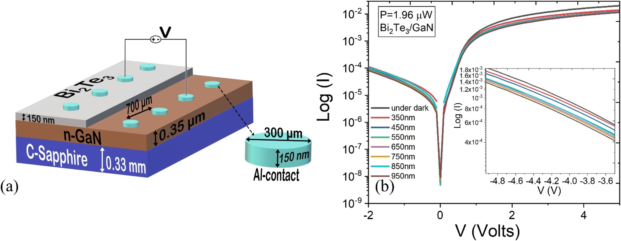 | ||
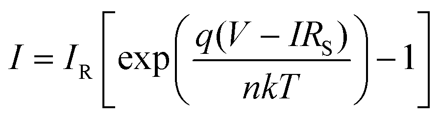
| Fig. 1 (a) Schematic of the device structure of Bi2Te3/n-GaN/S. (b) Plot of the semi-log (I–V) characteristics for the Bi2Te3/n-GaN heterojunction device under dark and illumination conditions when the wavelength of the irradiating wavelength of the light was varied from 350 nm to 950 nm at a constant incident light power of 1.96 μW; inset shows the reverse saturation current in the reverse bias (V) = −4.8 V to −3.6 V. | ||
3. Results and discussion
3.1 Material and microstructural study of the Bi2Te3 TI film grown on n-GaN
The detailed microstructural study of the Bi2Te3 TI film grown on n-GaN was done by XRD and SEM. The morphology and the vibration modes were studied using AFM and Raman spectroscopy. The material study of the Bi2Te3 TI film is discussed with the results provided in the ESI (refer to Fig. S2 and S3 in the ESI†).3.2 Electrical transport study
 | (1) |
 | (2) |
From eqn (S2) (refer to the ESI†) and by taking the slope of the semi-log (I–V) characteristics (Fig. S5 in the ESI†) at the saturation voltage, we get the ideality factor as n ≈ 3.88. The device area was 0.0049 cm2, while A* is the effective Richardson constant for n-GaN, which is 26.4 A cm−2 K−2,41 and φb is the barrier height. The barrier height calculated from the by I–V method using eqn (2) was thus determined to be 0.542 eV.
The contour of the photon energy of the incident light (E) was plotted against the electric current (I) at different driving voltages in Fig. 2a. The photon energy of incident light was calculated using eqn (3) as:
 | (3) |
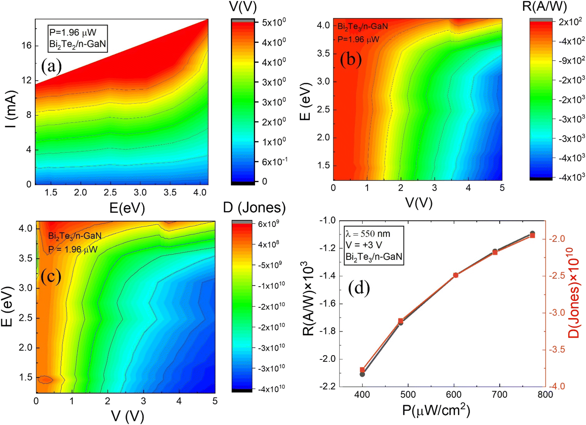 | ||
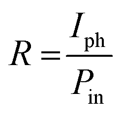
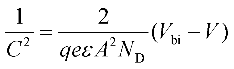
| Fig. 2 (a) Contour plot showing the current–energy (I–E) plot versus the driving voltage (V), measured for the voltage range from V = 0–5 V for the Bi2Te3/n-GaN heterojunction device, where E is the incident photon energy of the light having a wavelength (λ) varied from 350 nm to 950 nm at 1.96 μW incident power. Contour plots showing the relation between the (b) energy-responsivity (E–R) versus the driving voltage (V) and (c) energy–detectivity (E–D) versus the driving voltage (V) for the Bi2Te3/n-GaN heterojunction device, at constant 1.96 μW incident power. (d) Plot of the responsivity–power density (R–PD) (in black) and detectivity–power density (D–PD) (in red) at a constant driving voltage of 3 V and wavelength of incident light (λ) of 550 nm. | ||
It was imperative to inquire about how this aberrant behaviour would affect the performance parameters of Bi2Te3/n-GaN heterojunction devices. Therefore, the responsivity (R) and detectivity (D) were calculated using eqn (4) and (5):
 | (4) |
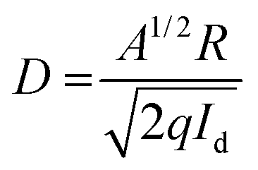 | (5) |
 | (6) |
51 for the Bi2Te3 TI film, the permittivity of free space (ε0) = 8.85 × 10⁻¹² F m−1, Vbi is the built-in potential, and ND is the carrier concentration in the film, while the barrier height (φb) of the heterojunction given by eqn (7) as: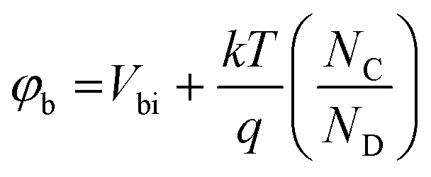 | (7) |
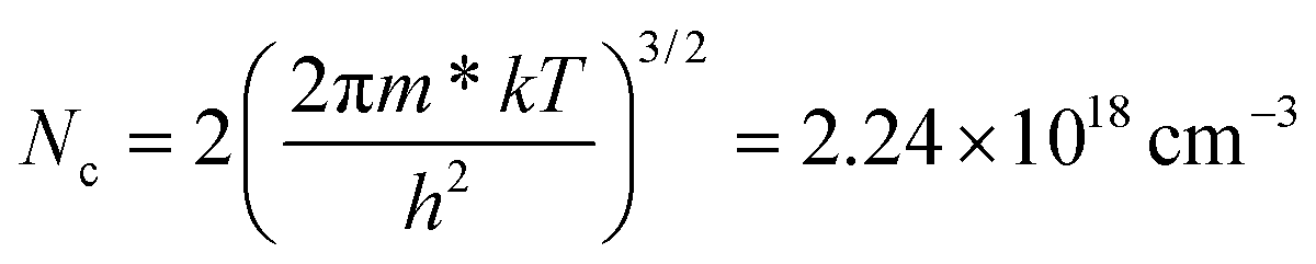 is the conduction band density of states at T = 300 K. Using eqn (6) and (7), the carrier concentration (ND) and the barrier height (φb) were calculated and found to be 3.89 × 1016 cm−3 and 1.80 eV. The barrier height obtained by the C–V measurement was comparatively higher than that measured by the I–V measurement. This discrepancy was primarily due to the surficial or interface defects, as observed in the C–V characteristics by the positive shift (Fig. 3a). This variation in barrier height might also be possible due to the image force and the barrier inhomogeneities as seen earlier.52
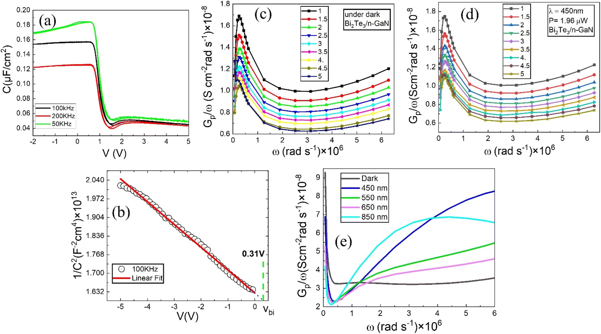 | ||
| Fig. 3 (a) Capacitance–voltage (C–V) characteristics for the Bi2Te3/n-GaN heterojunction under dark conditions at constant frequencies of 50, 100, and 200 kHz with the driving voltage from −2 V to +5 V. (b) Plot of 1/C2–V for the Bi2Te3/n-GaN heterojunction at 100 kHz frequency, with the intercept on the x-axis showing the built-in voltage (Vbi). (c) Plot of the conductance/radial frequency (Gp/ω) versus radial frequency (ω) for the Bi2Te3/n-GaN heterojunction, measured for the voltage biasing from +1 V to +5 V (interval of 0.5 V) under the dark conditions and (d) under light (λ = 450 nm, power = 1.96 W). (e) Conductance/radial frequency (Gp/ω) versus radial frequency (ω) plot for the Bi2Te3/n-GaN heterojunction at a constant positive bias of 0.5 V under the dark and illuminated conditions (∼450–850 nm, P = 1.96 μW). | ||
The 1/C2–V plot for the Bi2Te3/n-GaN heterojunction (Fig. 3b) showed a linear relation in the reverse bias of the Bi2Te3/n-GaN heterojunction. The good linear fitting in the reverse bias indicated the near absence of surface states, which affected the linearity of the 1/C2–V plot in the case of the charging and discharging of the traps.53 The capacitance–frequency (C–f) plot (refer to Fig. S7b in the ESI†) showed an almost linear decrease in the capacitance under reverse bias, without any major peak, confirming the negligible presence of traps in this region.53 To further study the trap characteristics, including the trap levels and the trap density, frequency (f) dependence conductance (Gp) measurements were performed. Here, Gp/ω versus the radial frequency (ω = 2πf) was plotted to study the trap density and trap response time.53 The Gp/ω–ω plot for the Bi2Te3/n-GaN heterojunction under the dark and under illuminated conditions in reverse bias was studied (refer to Fig. S7c and S7d in the ESI†), and it was observed that Gp/ω monotonically decreased without any peaks, with the least dependence on the negative biasing at a higher frequency. A similar behaviour for the heterojunction was observed by the Gp/ω–ω plot, under both dark and illuminated conditions (refer to Fig. S7c and d in the ESI†). The negative biasing reinforces the negligible charge and discharge of the trapping process. The Gp/ω–ω plot for the Bi2Te3/n-GaN heterojunction in positive bias is shown in Fig. 3c and d for the voltage range +1 V to +5 V (interval of 0.5 V), under both dark and illuminated conditions (λ = 450 nm, P = 1.96 μW). A single Gp/ω sharp peak at the same frequency (ω = 2.5 × 10⁶ rad s−1) was observed within the measured voltage bias. The peaks implied the presence of a trap state with a single discrete energy. The Gp/ω peaks here decreased with the increase in the applied positive bias. Here, the peaks in Gp/ω represented the trap density, which reduced with increasing the applied positive bias. The illuminated Bi2Te3/n-GaN heterojunction (λ = 450 nm, P = 1.96 μW) showed almost the same Gp/ω–ω characteristics without any shifting of the Gp/ω peaks. This similar peak pattern was also observed for all the measured ranges of incident light wavelength (λ) from 450–950 nm. A shift in the Gp/ω peaks was not observed, which was expected after the illumination due to the rise in temperature as observed in the previous study.53 The Gp/ω–ω characteristics for the Bi2Te3/n-GaN heterojunction at +0.5 V bias voltage are shown in Fig. 3e, under dark and illuminated conditions (λ = 450–850 nm, P = 1.96 μW). Interestingly, only a single Gp/ω minimum was observed at the frequency ω = 0.5 × 10⁶ rad s−1 when the wavelength was varied over the range from 450–850 nm, signifying the minimum density of traps. The illuminated Gp/ω minima peak, however, dipped more in comparison to the dark one, due to the decrease in the conductivity under illumination (Fig. 3e). This dip in the peak was consistent with a reduction in current seen in the I–V results of the Bi2Te3/n-GaN heterojunction (Fig. 1b). This reduction in current could also be observed from the (I–E) versus V contour plot at higher incident photon wavelength (Fig. 1b) due to the polycrystalline Bi2Te3 TI film in the Bi2Te3/n-GaN heterojunction.
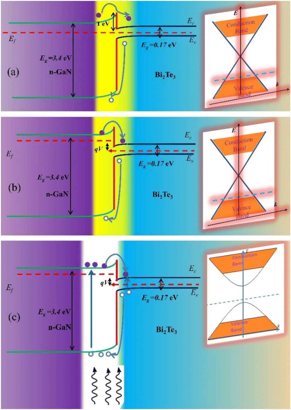 | ||
| Fig. 4 Energy band diagram of the Bi2Te3/n-GaN heterojunction at (a) thermal equilibrium, where a space charge region was created due to the diffusion of carriers at the junction resulting in built-in potential at the junction, (b) forward biasing under the dark conditions with the Dirac cone surface state of the polycrystalline Bi2Te3 TI film, and (c) forward bias under the influence of the light photons, where the shape of the Dirac cone changed with the opening of bandgap at the surface of the polycrystalline Bi2Te3 TI film under illumination. | ||
Conceptually, the opening of the bandgap of the Dirac cone was substantiated for graphene and TIs under the illumination with polarized light.45,47,48,55 These band openings under circularly polarized light have also been observed through experimental time and angle-resolved photoemission spectroscopy (ARPES) of Bi2Se3 TI thin films.49 However, contrary to the observation under polarized light, the phenomenon observed here was due to the unpolarized light, which makes it more interesting. The polycrystalline Bi2Te3 film has the same rhombohedral crystal structure as the single crystal in the space group D3d5 (R![[3 with combining macron]](https://www.rsc.org/images/entities/char_0033_0304.gif) m)56 with the time-reversal symmetry. Therefore, our polycrystalline had a similar Dirac cone-like structure as the single-crystal Bi2Te3 and behaved similarly under the influence of light with the opening of the bandgap. Due to the intrinsic defects present in the undoped Bi2Te3 films, their Fermi level lay in the conduction band of the bulk, giving the material a metallic nature, and therefore the thermal effect caused by the illumination could not be completely ignored. This thermal effect enhanced the resistance through electron–phonon scattering.46 Nevertheless, the instant positive resistance effect could not be seen in the Gp/ω–ω characteristics (Fig. 3c & d), where the peak shifting was not apparent. The thermal artefact was also not seen recently in a photodetection study of polycrystalline Bi2Te3 TI films due to the lack of a long tail in the transient response.46 Furthermore, a weak broadening of the topological surface state with the temperature and negligible anomalies in the dispersion of the state were observed for the Bi2Te3 TI recently.57 Therefore, this remarkably weak electron–phonon coupling in the Bi2Te3 films further excluded the thermal origin of the increase in the resistance in our experiment.
m)56 with the time-reversal symmetry. Therefore, our polycrystalline had a similar Dirac cone-like structure as the single-crystal Bi2Te3 and behaved similarly under the influence of light with the opening of the bandgap. Due to the intrinsic defects present in the undoped Bi2Te3 films, their Fermi level lay in the conduction band of the bulk, giving the material a metallic nature, and therefore the thermal effect caused by the illumination could not be completely ignored. This thermal effect enhanced the resistance through electron–phonon scattering.46 Nevertheless, the instant positive resistance effect could not be seen in the Gp/ω–ω characteristics (Fig. 3c & d), where the peak shifting was not apparent. The thermal artefact was also not seen recently in a photodetection study of polycrystalline Bi2Te3 TI films due to the lack of a long tail in the transient response.46 Furthermore, a weak broadening of the topological surface state with the temperature and negligible anomalies in the dispersion of the state were observed for the Bi2Te3 TI recently.57 Therefore, this remarkably weak electron–phonon coupling in the Bi2Te3 films further excluded the thermal origin of the increase in the resistance in our experiment.
The previously proposed model to describe the negative photoconductivity (NPC) effect28,58 explained the trapping of electrons by a vacant localized state of random fluctuations in the local potential barrier.46 According to this gap-state transition model, the negative photoconduction should be observed because of the trapping of the photoexcited electrons,33,34 with the occurrence of negative photoconduction at a particular photon energy. However, it was observed that the intrinsic negative photoconductivity response for our Bi2Te3 TI heterojunction devices prevailed over a broad range of incident light wavelengths and power. Therefore, based on our experimental evidence, we emphasize that the observed aberrant photoelectric effect in our Bi2Te3/n-GaN heterojunction devices was due to the intrinsic feature of the polycrystalline Bi2Te3 TI film under illumination. This new mechanism involved in our results was certainly due to the opening of the bandgap at the Dirac cone surface of the polycrystalline Bi2Te3 TI film under the influence of unpolarized light; thereby decreasing the surface charge mobility and increasing the resistance as compared to the dark current, and therefore resulting in an aberrant photoconduction in our Bi2Te3/n-GaN heterojunction devices. We observed a considerable negative photoresponse and high responsivity for our Bi2Te3/n-GaN heterojunction device. NPC devices have been lately employed for the fabrication of humidity and light sensors.59 Due to its high responsivity, our Bi2Te3/n-GaN device can likely find applications in highly sensitive photodetectors60 and non-volatile memories.61–63 Also, perhaps the bandgap-opening phenomenon in the presence of the unpolarized light can be employed in retinomorphic devices.64
4. Conclusion
The Bi2Te3/n-GaN heterojunction was realized by growing a thin polycrystalline Bi2Te3 TI film on an n-GaN template (on sapphire). The I–V characteristics confirmed the rectifying nature of the heterojunction device. The electrical properties of the heterojunction were studied by I–V, C–V, C–f, and Gp/ω–ω plots under both the dark and illuminated conditions. The optical study of the Bi2Te3/n-GaN heterojunction devices revealed an aberrant photoelectric effect under a broad range of incident light wavelengths and power. The negative photoconductance was observed in the I–V characteristics with an increase in resistance under the influence of unpolarized light in the forward bias. The good responsivity and detectivity of −3.8 × 10³ A W−1 and −3.86 × 10¹⁰ Jones were observed in the working range of the device. The observed aberrant photoelectric effect under unpolarized illumination was due to a photon-induced gap at the Dirac point on the polycrystalline Bi2Te3 TI film surface, resulting in negative photoconductivity. The observed aberrant photoelectric effect can be significant in realizing highly sensitive photodetectors and non-volatile memories; while the band gap opening can be employed in applications in retinomorphic devices with atypical ranges of operation.Author contributions
P. K. and F. A. conceived the initial research idea planned the study. P. K. and F. A. did the electrical analysis. F. A., K. K., P. K. wrote the manuscript. R. K. analyzed the ultrafast data.Conflicts of interest
No conflict of interest from any of the authors.Acknowledgements
The authors would like to thank DST, Govt. of India (CRG/2022/000070) for providing the financial support to carry out this work. VLSI Lab, Department of Electronics and Communication Engineering, IIIT Allahabad for electrical characterization. CIR, MNNIT-Allahabad for providing the material characterization facilities. My colleague Dr. Sanjay Sharma, Spintronics and Magnetic Materials Laboratory, IIIT Allahabad, for helping me with the technical drawing of the device schematic.References
- B. Zhang and Y. Liu, Chin. Sci. Bull., 2014, 59, 1251–1275 CrossRef CAS.
- B.-J. Kim, G. Yang, H.-Y. Kim, K. H. Baik, M. A. Mastro, J. K. Hite, C. R. Eddy, F. Ren, S. J. Pearton and J. Kim, Opt. Express, 2013, 21, 29025–29030 CrossRef PubMed.
- M. Kumar, H. Jeong, K. Polat, A. K. Okyay and D. Lee, J. Phys. D: Appl. Phys., 2016, 49, 275105 CrossRef.
- Y.-C. Yao, C.-Y. Huang, T.-Y. Lin, L.-L. Cheng, C.-Y. Liu, M.-T. Wang, J.-M. Hwang and Y.-J. Lee, Microelectron. Eng., 2015, 138, 1–6 CrossRef CAS.
- Y. Jiang, Y. Li, Y. Li, Z. Deng, T. Lu, Z. Ma, P. Zuo, L. Dai, L. Wang and H. Jia, Sci. Rep., 2015, 5, 1–7 CrossRef CAS.
- H. J. Chang, T. W. Chen, J. W. Chen, W. C. Hong, W. C. Tsai, Y. F. Chen and G. Y. Guo, Phys. Rev. Lett., 2007, 98, 136403 CrossRef CAS.
- L. Zhang, T. A. Hill, C.-H. Teng, B. Demory, P.-C. Ku and H. Deng, Phys. Rev. B: Condens. Matter Mater. Phys., 2014, 90, 245311 CrossRef.
- A. K. Viswanath, J. Nanosci. Nanotechnol., 2014, 14, 1253–1281 CrossRef CAS.
- C.-J. Lee, S.-B. Kang, H.-G. Cha, C.-H. Won, S.-K. Hong, B.-J. Cho, H. Park, J.-H. Lee and S.-H. Hahm, Jpn. J. Appl. Phys., 2015, 54, 06FF08 CrossRef.
- F. Lin, S.-W. Chen, J. Meng, G. Tse, X.-W. Fu, F.-J. Xu, B. Shen, Z.-M. Liao and D.-P. Yu, Appl. Phys. Lett., 2014, 105, 73103 CrossRef.
- A. Gundimeda, S. Krishna, N. Aggarwal, A. Sharma, N. D. Sharma, K. K. Maurya, S. Husale and G. Gupta, Appl. Phys. Lett., 2017, 110, 103507 CrossRef.
- M. Rais-Zadeh, V. J. Gokhale, A. Ansari, M. Faucher, D. Théron, Y. Cordier and L. Buchaillot, J. Microelectromech. Syst., 2014, 23, 1252–1271 CAS.
- M. Wu, Z. Gong, A. J. C. Kuehne, A. L. Kanibolotsky, Y. J. Chen, I. F. Perepichka, A. R. Mackintosh, E. Gu, P. J. Skabara and R. A. Pethrick, Opt. Express, 2009, 17, 16436–16443 CrossRef CAS PubMed.
- S. Dhar, O. Brandt, M. Ramsteiner, V. F. Sapega and K. H. Ploog, Phys. Rev. B, 2005, 72, 245203 CrossRef.
- Y. L. Chen, J. G. Analytis, J. H. Chu, Z. K. Liu, S. K. Mo, X. L. Qi, H. J. Zhang, D. H. Lu, X. Dai and Z. Fang, Science, 2009, 325, 178–181 CrossRef CAS PubMed.
- K. Zheng, L.-B. Luo, T.-F. Zhang, Y.-H. Liu, Y.-Q. Yu, R. Lu, H.-L. Qiu, Z.-J. Li and J. C. A. Huang, J. Mater. Chem. C, 2015, 3, 9154–9160 RSC.
- P. H. Le, K. H. Wu, C. W. Luo and J. Leu, Thin Solid Films, 2013, 534, 659–665 CrossRef CAS.
- Y. Li, G. Wang, X. Zhu, M. Liu, C. Ye, X. Chen, Y. Wang, K. He, L. Wang and X. Ma, Adv. Mater., 2010, 22, 4002–4007 CrossRef CAS.
- D. Minjiang, G. Hu, L. Li and Y. Zhang, Nano Energy, 2018, 50, 544–551 CrossRef.
- X. Zhang, J. Wang and S.-C. Zhang, Phys. Rev. B: Condens. Matter Mater. Phys., 2010, 82, 245107 CrossRef.
- J. M. Shao, H. Li and G. W. Yang, Nanoscale, 2014, 6, 3513–3517 RSC.
- J. Ma, K. Deng, L. Zheng, S. Wu, Z. Liu, S. Zhou and D. Sun, 2D Mater., 2019, 6, 32001 CrossRef CAS.
- E. Kioupakis, M. L. Tiago and S. G. Louie, Phys. Rev. B: Condens. Matter Mater. Phys., 2010, 82, 245203 CrossRef.
- I. T. Witting, T. C. Chasapis, F. Ricci, M. Peters, N. A. Heinz, G. Hautier and G. J. Snyder, Adv. Electron. Mater., 2019, 5, 1800904 CrossRef.
- J. D. Yao, J. M. Shao, S. W. Li, D. H. Bao and G. W. Yang, Sci. Rep., 2015, 5, 1–8 Search PubMed.
- M. Y. Pang, W. S. Li, K. H. Wong and C. Surya, J. Non-Cryst. Solids, 2008, 354, 4238–4241 CrossRef CAS.
- R. P. Prasankumar and A. J. Taylor, Optical techniques for solid-state materials characterization, CRC Press, 2016 Search PubMed.
- P.-C. Wei, S. Chattopadhyay, M.-D. Yang, S.-C. Tong, J.-L. Shen, C.-Y. Lu, H.-C. Shih, L.-C. Chen and K.-H. Chen, Phys. Rev. B: Condens. Matter Mater. Phys., 2010, 81, 45306 CrossRef.
- M. Liao, Y. Koide, J. Alvarez, M. Imura and J.-P. Kleider, Phys. Rev. B: Condens. Matter Mater. Phys., 2008, 78, 45112 CrossRef.
- A. S. Chaves and H. Chacham, Appl. Phys. Lett., 1995, 66, 727–729 CrossRef CAS.
- H. Nakanishi, K. J. M. Bishop, B. Kowalczyk and A. Nitzan, Nature, 2009, 460, 371–375 CrossRef CAS PubMed.
- X. Zhang, J. Jie, Z. Wang, C. Wu, L. Wang, Q. Peng, Y. Yu, P. Jiang and C. Xie, J. Mater. Chem., 2011, 21, 6736–6741 RSC.
- E. Baek, T. Rim, J. Schütt, C. Baek, K. Kim, L. Baraban and G. Cuniberti, Nano Lett., 2017, 17, 6727–6734 CrossRef CAS PubMed.
- Y. Yang, X. Peng, H.-S. Kim, T. Kim, S. Jeon, H. K. Kang, W. Choi, J. Song, Y.-J. Doh and D. Yu, Nano Lett., 2015, 15, 5875–5882 CrossRef CAS PubMed.
- G. Kim, I. G. Kim, J. H. Baek and O. K. Kwon, Appl. Phys. Lett., 2003, 83, 1249–1251 CrossRef CAS.
- F. Ahmad, K. Kandpal, N. Kumar, R. Kumar and P. Kumar, IEEE Trans. Electron Devices, 2020, 67(12), 5388–5395 CAS.
- F. Ahmad, S. Singh, S. K. Pundir, R. Kumar, K. Kandpal and P. Kumar, J. Electron. Mater., 2020, 1–8 Search PubMed.
- C.-Y. Chang, Y. K. Fang and S. M. Sze, Solid-State Electron., 1971, 14, 541–550 CrossRef CAS.
- Y. Liu , in IOP Conference Series: Materials Science and Engineering, IOP Publishing, 2020, vol. 738, p. 12007.
- F. Ahmad, R. Singh, P. K. Misra, N. Kumar, R. Kumar and P. Kumar, J. Electron. Mater., 2018, 47(12), 6972–6983 CrossRef CAS.
- N. N. K. Reddy and V. R. Reddy, Bull. Mater. Sci., 2012, 35, 53–61 CrossRef CAS.
- A. Turut, H. Doğan and N. Yıldırım, Mater. Res. Express, 2015, 2, 96304 CrossRef.
- P. Ghaemi, R. S. K. Mong and J. E. Moore, Phys. Rev. Lett., 2010, 105(16), 166603 CrossRef PubMed.
- B. Poudel, Y. Ma, Y. Lan, B. Yu, X. Yan, D. Wang, Z. Ren, Q. Hao, A. Minnich, A. Muto, D. Vashaee, X. Chen, G. Chen, J. Liu and M. S. Dresselhaus, Science, 2008, 320(5876), 634–638 CrossRef CAS.
- M. Busl, G. Platero and A.-P. Jauho, Phys. Rev. B: Condens. Matter Mater. Phys., 2012, 85, 155449 CrossRef.
- H. Zhang, J. Yao, J. Shao, H. Li, S. Li, D. Bao, C. Wang and G. Yang, Sci. Rep., 2014, 4, 1–5 Search PubMed.
- O. V. Kibis, Phys. Rev. B: Condens. Matter Mater. Phys., 2010, 81, 165433 CrossRef.
- Y. Zhou and M.-W. Wu, Phys. Rev. B: Condens. Matter Mater. Phys., 2011, 83, 245436 CrossRef.
- Y. H. Wang, H. Steinberg, P. Jarillo-Herrero and N. Gedik, Science, 2013, 342, 453–457 CrossRef CAS.
- S. M. Sze, Semiconductor devices: physics and technology, John Wiley & Sons, 2008 Search PubMed.
- J. Dheepa, R. Sathyamoorthy, A. Subbarayan, S. Velumani, P. J. Sebastian and R. Perez, Sol. Energy Mater. Sol. Cells, 2005, 88, 187–198 CrossRef CAS.
- I. Hussain, M. Y. Soomro, N. Bano, O. Nur and M. Willander, J. Appl. Phys., 2012, 112, 64506 CrossRef.
- Y. Shi, Q. Zhou, A. Zhang, L. Zhu, Y. Shi, W. Chen, Z. Li and B. Zhang, Nanoscale Res. Lett., 2017, 12, 1–6 CrossRef PubMed.
- F. Ahmad, R. Kumar, S. S. Kushvaha, M. Kumar and P. Kumar, npj 2D Mater. Appl., 2022, 6, 12 CrossRef CAS.
- B. M. Fregoso, Y. H. Wang, N. Gedik and V. Galitski, Phys. Rev. B: Condens. Matter Mater. Phys., 2013, 88, 155129 CrossRef.
- D. Hsieh, Y. Xia, L. Wray, D. Qian, A. Pal, F. Meier, J. Osterwalder, G. Bihlmayer, C. L. Kane and Y. S. Hor, Science, 2009, 323, 919–922 CrossRef CAS PubMed.
- Z.-H. Pan, A. V. Fedorov, D. Gardner, Y. S. Lee, S. Chu and T. Valla, Phys. Rev. Lett., 2012, 108, 187001 CrossRef.
- H. J. Stocker, Phys. Rev. Lett., 1967, 18, 1197 CrossRef CAS.
- J.-X. Qin, X.-G. Yang, C.-F. Lv, Y.-Z. Li, X. X. Chen, Z.-F. Zhang, J.-H. Zang, X. Yang, K.-K. Liu and L. Dong, J. Phys. Chem. Lett., 2021, 12, 4079–4084 CrossRef CAS PubMed.
- N. K. Tailor, C. A. Aranda, M. Saliba and S. Satapathi, ACS Mater. Lett., 2022, 4, 2298–2320 CrossRef CAS.
- Y. Dong, K. M. Dowling, S. P. Hau-Riege, A. Conway, L. F. Voss and S. Rakheja, J. Appl. Phys, 2022, 113, 134504 CrossRef.
- X. Lin, X. Huang, Q. Zhang, J. Yi, S. Liu and Q. Liang, Appl. Phys. Lett, 2023, 123(18), 180501 CrossRef CAS.
- E. Faella, K. Intonti, L. Viscardi, F. Giubileo, A. Kumar, H. T. Lam, K. Anastasiou, M. F. Craciun, S. Russo and A. Di Bartolomeo, Nanomaterials, 2022, 12, 1886 CrossRef CAS PubMed.
- Z. Zhang, S. Wang, C. Liu, R. Xie, W. Hu and P. Zhou, Nat. Nanotechnol., 2022, 17, 27–32 CrossRef CAS PubMed.
Footnote |
| † Electronic supplementary information (ESI) available. See DOI: https://doi.org/10.1039/d3nr03360k |
| This journal is © The Royal Society of Chemistry 2024 |