
 Open Access Article
 This Open Access Article is licensed under a
 Creative Commons Attribution 3.0 Unported Licence
Plasmonic Fabry–Pérot nanocavities produced via solution methods†
Stylianos
Kioumourtzoglou
a,
Robert
Berical-Vadell
a,
Vitor R.
Silveira
a,
Dan
Li
b,
Mikaela
Görlin
 b and
Jacinto
Sá
*ac
b and
Jacinto
Sá
*ac
aDepartment of Chemistry-Ångström, Physical Chemistry Division, Uppsala University, 751 20 Uppsala, Sweden. E-mail: Jacinto.sa@kemi.uu.se
bDepartment of Chemistry-Ångström, Structural Chemistry Division, Uppsala University, 751 20 Uppsala, Sweden
cInstitute of Physical Chemistry, Polish Academy of Sciences, 01-224 Warsaw, Poland
First published on 1st May 2024
Abstract
Plasmonic nanomaterials have garnered considerable attention in the scientific community due to their applicability in light-mediated technologies, owing to tunability, large optical cross-sections and scalability. Plasmonic nanoparticles with uniform morphology exhibit substantial optical cross-sections but limited energy absorption windows, reducing effectiveness for applications using polychromatic illumination like sunlight. Integrating plasmonics electrodes with a Fabry–Pérot nanocavity is a promising approach to broaden the absorption energy range of single morphology particles. Traditionally, the fabrication of these nanocavities involves clean room processes, posing scalability challenges and limiting the materials' scope. This study presents a successful approach for enhancing light absorption in a plasmonic photoelectrode system through a Fabry–Pérot nanocavity created using bottom-up solution methods. This approach technique overcomes some of the existing scalability issues while enabling the fabrication of a photocathode that can be rendered semitransparent or opaque. Such versatility opens up many application possibilities for these photosystems, from photocatalysis to optical devices.
Plasmonic materials have received considerable attention as a novel light-driven system for optoelectronics,1–5 photovoltaics,4,6,7 photocatalysis8–12 and others.1,13 Plasmonic nanoparticles absorb light through a unique photophysical process called localised surface plasmon resonance (LSPR). LSPR is associated with the collective oscillation of electrons in noble metal nanoparticles (such as gold and silver) when illuminated. The interaction between light and metal nanoparticles leads to the excitation of surface plasmons, which oscillate electrons at the metal surface, resulting in enhanced electromagnetic fields in those areas. The localised electromagnetic fields can be used for sensing, imaging and optoelectronics. The decoherence of the electron oscillations forms a non-Fermi–Dirac population of excited carriers (i.e. hot carriers), which can be leveraged for photocatalysis and photovoltaics. At the same time, the heat resultant from their recombination can be used for thermal catalysis and phototherapy.
LSPR occurs at the nanoscale and is highly sensitive to the nanoparticles' size, shape and surrounding environment. Despite their large optical cross-sections, a 2D electrode consisting of sub-monolayers of plasmonic nanoparticles with uniform morphology cannot efficiently harvest polychromatic light, such as sunlight.14–16 Photoelectrodes with three-dimensional architectures were developed and applied to improve light utilisation efficiency,17–20 but they are complex and challenging to scale. It is, therefore, paramount to develop approaches to increase 2D electrodes/devices' energy absorption range.
Shi et al.21 demonstrated a highly efficient broadband light-harvesting photoanode with a single plasmonic particle size. Their system consisted of an Au-film/TiO2/Au NPs (nanoparticles) structure. The device showed a strong coupling between the Fabry–Pérot nanocavity modes and LSPR, which they exploited to broaden their system absorption spectrum and increase the water-splitting quantum yield.
A Fabry–Pérot cavity22 is a fundamental optical structure named after the French physicists Charles Fabry and Alfred Pérot, who developed it in the late 19th century. Fabry–Pérot cavities are optical resonators or interferometers with two parallel and highly reflective surfaces (e.g. mirrors or other reflective structures). The basic Fabry–Pérot cavity configuration consists of an entrance mirror, a partially transmitting internal mirror, and an exit mirror. Light enters the cavity through the entrance mirror, reflects between the two mirrors multiple times, and then exits through the partially transmitting internal mirror. The interference of the reflected beams creates constructive and destructive interference patterns, forming a series of resonant optical modes within the cavity. The design and characteristics of Fabry–Pérot cavities make them versatile tools in optical systems and devices. Fabry–Pérot cavities are widely used in optics and photonics for various applications, including interferometry, laser cavities, etc.
The electrodes/devices are commonly produced via a top-down methodology requiring sophisticated equipment, often located in a clean room environment. Consequently, they are challenging to scale and adapt. Additionally, despite the advancements,23 top-down approaches limit the materials’ scope. Therefore, it is highly desirable to develop complementary bottom-up manufacturing of such systems that can be processed from solution. Bottom-up approaches can leverage a wider breadth of plasmonic nanoparticle morphologies and dielectric materials, consequently expanding the range of applications. Furthermore, bottom-up approaches are less costly and more versatile.
Herein, a methodology for preparing an electrode via bottom-up solution methods, which can be adapted and scaled, is presented. The electrode consisted of FTO/metal film/CuSCN/Au NPs. The electrodes significantly enhanced the energy absorption window while acting as a potential photo-cathode. The design can be made semitransparent or opaque, offering solutions to various applications. Since single plasmonic nanoparticle morphologies have characteristically narrow band absorption,24 our device was constructed as a Fabry–Pérot nanocavity resonator to broaden their absorption without changing their morphology. A significant aspect of the approach is that it can be adapted to any plasmonic nanoparticles since the dielectric layer contains selective anchoring groups to attach the plasmonic particles.
The experimental details associated with synthesising Au NPs can be found in the ESI.† We synthesised them via a method reported elsewhere.25 Fig. S1a (ESI†) shows the dynamic light scattering (DLS) spectrum of the Au NPs. The average particle size was estimated to be 8 ± 2 nm. The Au NPs monodispersity was confirmed by the single peak in the DLS spectrum and the low polydispersity index (PDI) of about 0.26. The average particle size and shape uniformity were further confirmed by SEM analysis, shown in Fig. 1 and Fig. S2 (ESI†). The images show a good distribution of particles in FTO with similar size (5–10 nm) and shape (spherical). The samples displayed a characteristic Au NPs LSPR peak centred at 515 nm with an intraband absorption tail below 500 nm (Fig. S1b, ESI†).
 | ||
| Fig. 1 Scanning electron microscopy (SEM) of the Au NPs deposited on high-resolution FTO glass to determine average particle size. | ||
The findings show that the starting plasmonic nanoparticles are homogeneous in morphology and size. Consequently, the devices manufactured from them are expected to have a narrow band absorption unless fabricated with a Fabry–Pérot nanocavity structure.15 This is noticeable by analysis of the UV-vis spectra in the absence of Fabry–Pérot nanocavity (Fig. S4, ESI†). Adding CuSCN to the FTO glass improved the transmission of the conductive glass by effectively reducing its reflectivity. Adding Au NPs increases the device absorption around the plasmonic resonance and intraband, consistent with the amount of Au NPs attached. Still, there was no significant optical enhancement in broadening the absorption energy range.
The Fabry–Pérot nanocavity fabrication steps are illustrated in Scheme 1. First, the FTO TEC 15 glass substrates (∼12–15 Ω sq−1) were cleaned by ultrasonication in a solution containing surfactant, double-deionized water, acetone and isopropanol. Then, the FTO substrates were treated with UV-ozone for 15 min. Three different categories of samples were fabricated: (i) samples with a reflective film on the backside of the FTO substrate (reference samples), (ii) samples with a semitransparent reflective film on top of the FTO substrate, and (iii) samples with a reflective film on top of the FTO substrate. The general structure of the nanocavity samples used was FTO/metallic film/CuSCN/Au NPs. The semitransparent metallic film consisted of 25 nm Au film, whereas the reflective film was a 100 nm Ag film. The metallic films were prepared by evaporation employing the LEICA EM MED202 (Leica Camera AG, Wetzlar, Germany).
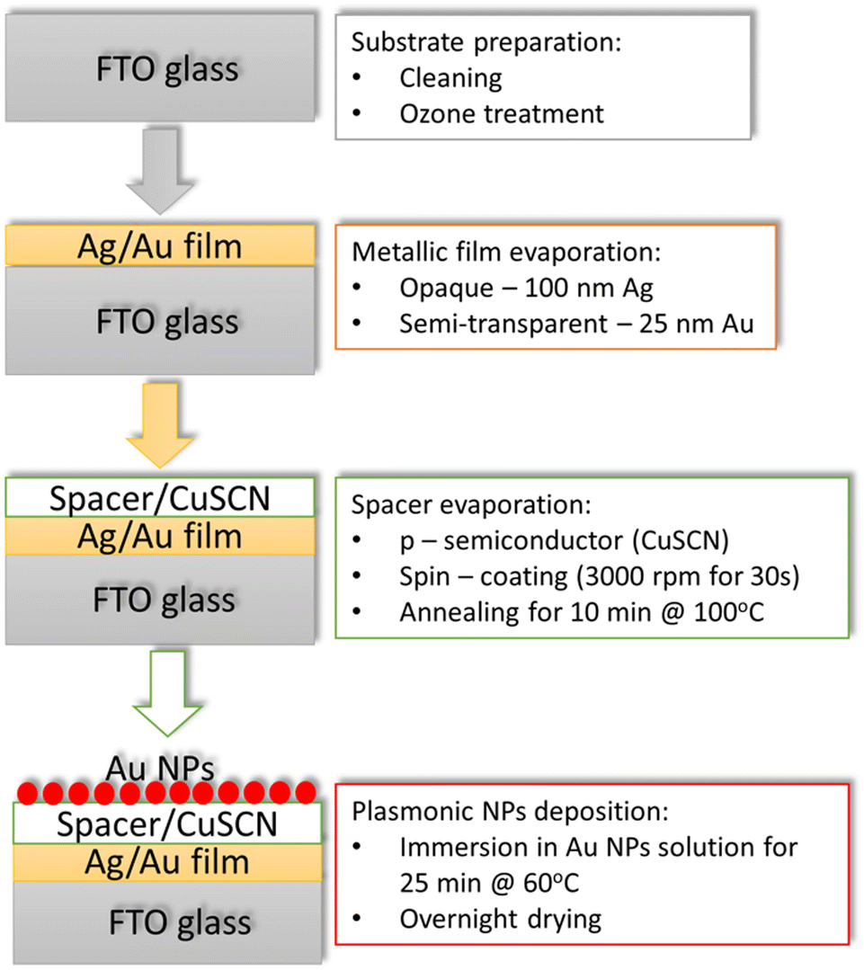 | ||
| Scheme 1 Schematic representation of the steps involved in the Fabry–Pérot nanocavity fabrication. | ||
In addition to broadening the device absorption energy range, we wanted to demonstrate that the system could act as a photo-cathode. Therefore, the dielectric layer should be a p-type semiconductor to extract hot holes from the plasmonic particles, which, in our case, was CuSCN. The CuSCN films were fabricated via spin coating using a precursor solution of 0.08 M of CuSCN powder diluted in diethyl sulfide (9.7 mg in 5 mL) to which we added 10 μL of 4-methoxy thiophenol that acts as a plasmonic attaching group via its S–H groups.26 The CuSCN layer was spin-coated onto the FTO substrates with a speed of 3000 rpm for 30 s and heated at 100 °C on a hotplate for 10 min, yielding CuSCN films about 30 nm thick.27 SEM analysis of the cross-section (Fig. S3, ESI†) revealed that the CuSCN layer has a thickness similar to the FTO layer on TEC15 glass, which is between 320–340 nm.28 A CuSCN layer between 250–300 nm fulfils the requirement that the dielectric layer thickness must be close to the light wavelength. The nanoparticle loading was then achieved by submerging the samples into an Au NPs solution (∼5 mM) for 25 min at 60 °C. After the Au NPs deposition, the samples were allowed to dry in air overnight.
Fig. 2 shows the optical absorption of the films. The reflectance spectra of the samples are shown in Fig. S5 (ESI†). The attachment of Au NPs to the CuSCN promoted by the 4-methoxy thiophenol molecules is observed by the appearance of an absorption peak centred at 609 nm. The shift in the LSPR peak is explained by the heterogenisation of the Au NPs and inhomogeneity in the dielectric layer thickness, consistent with previously published electrodes.29 Note that without the semitransparent 25 nm Au metal film, the absorption across the visible range never exceeded 0.4.
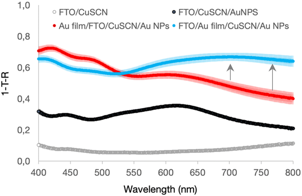 | ||
| Fig. 2 Electrodes optical absorption comparison. The trace shade represents the error originating from variability in sample fabrication. UV-vis spectra of the semitransparent samples: FTO/CuSCN (grey line), FTO/CuSCN/Au NPs (black line), Au film/FTO/CuSCN/Au NPs (red line) and FTO/Au film/CuSCN/Au NPs (blue line). The arrows indicate the gain in optical absorption due to the Fabry–Pérot nanocavity. | ||
The addition of the semitransparent 25 nm Au metal film significantly affected the electrode absorption, increasing the electrode absorption by about 0.3–0.5. However, when the Au film is on top of FTO and thus in an arrangement where the Fabry–Pérot nanocavity can occur, there is a further enhancement in the absorption between 550–800 nm, as highlighted by the arrows in Fig. 2, suggesting coupling of the Au NPs LSPR absorption with the Au film. This increase in absorption cannot be justified by changes in film morphology because, according to atomic force microscopy (AFM) analysis (Fig. S6, ESI†), this was not significantly affected. According to the AFM, the films' roughness decreased as additional layers were added, but not to the point that this could significantly affect the overall scattering.30 All films with CuSCN were very smooth with a roughness root mean square (RMS) of 4.98 nm, considering they were fabricated on FTO that has an RMS of 30.5 nm, which is a notably rough substrate, corroborating CuSCN properties to make thin and smooth films.26
Enhancements of plasmonic optical absorption in the presence of metallic films have been observed in gap mode plasmonic coupling with metal film31–33 and in Fabry–Pérot nanocavity structures.21 Gap mode devices enhance the optical absorption of the metallic film and the nanoparticles by inserting an ultrathin gap between the two structures, generally <10 nm. The gap can be a thin dielectric layer32,33 or simply a physical separation.31 Independently on how they are fabricated, the gap mode devices' optical spectra have a characteristic enhancement in the absorption peaks of the metal film and nanoparticles intensity but do not significantly broaden the peaks absorption. This is the most significant difference between the spectra compared to Fabry–Pérot nanocavity, which enhances the absorption of the individual components and broadens the absorption spectrum via shifting of the central absorption peak to the red and inducing a new absorption band to the blue of the LSPR peak.34,35 Therefore, the observed enhancement is consistent with forming a Fabry–Pérot nanocavity, which broadens light absorption in some parts by as much as 20%. The observation is also consistent with Shi et al. findings,21 where they observed the most significant optical absorption when the nanocavity modes overlap with the Au NPs LSPR absorption.
Because of the fabrication methods and FTO substrate roughness, it is reasonable to expect some inhomogeneity in the dielectric layer thickness. Inhomogeneity in the dielectric thickness can induce some broadening but is not the main culprit for the findings because the broadening in the nanocavity is much more considerable than what was observed when the Au NPs were deposited on the CuSCN with the semitransparent film, where inhomogeneity in the dielectric thickness is also expected.
The finding demonstrates that Fabry–Pérot nanocavities can be created from bottom-up solution-based methods, even on semitransparent electrodes. Semitransparent electrodes enable optical spectroscopic measurements in transmission mode,36 energy transfer processes, and photochemical reactions with back-side illumination (the most common, at least in academic settings).37 To validate the proposed strategy's relevance, it is essential to establish that (i) the presence of the nanocavity increases light absorption at different wavelengths and (ii) that more charge can be extracted from devices, in this case, hot holes.
Power-dependent light absorbance measurements were performed to substantiate the nanocavity optical absorption properties. Fig. 3 shows the absorbance of the FTO/Au NPs sample and FTO/Au film/CuSCN/Au NPs under different CW laser power at resonant (excitation at 532 nm) and non-resonant excitation (excitation at 630 nm). Note that the FTO/Au NPs (reference sample) have significantly higher Au NPs loading because the loading is not limited by the Au NPs attachment to the CuSCN; therefore, one is to expect a high signal when exciting Au NPs resonantly.
 | ||
| Fig. 3 Power-dependent light absorbance for the FTO/Au NPs sample (red trace) and FTO/Au film/CuSCN/Au NPs (blue trace). (a) Using the 532 nm CW laser (resonant excitation); and (b) employing the 635 nm CW laser (non-resonant excitation). | ||
Under resonant excitation (Fig. 3a), the presence of the cavity led to an increase of about 20% in light absorption, which is significant if one considers that the FTO/Au NPs device has a higher loading of Au NPs for the abovementioned reasons. When the experiments were performed using non-resonant excitation (Fig. 3b), the enhancement was about 40%. Noticeably, the light uptake for the sample with the nanocavity did not change significantly between the two excitation modes, corroborating that the nanocavity expands the optical absorption range.
To establish that the Fabry–Pérot nanocavity electrode can act as a photocathode over a broad energy range, we performed transient absorption spectroscopy (TAS). Optical excitation of the plasmon resonance widens its optical absorption peak, forming a bleach signal around the excitation wavelength and two positive winglets on either side of the bleach signal.38–41 Kinetic traces extracted at the maximum of the winglets or minimum of the bleach provide information on plasmon excitation efficiency (delta absorption (ΔA) at time zero) and hot carriers' lifetime. The latter includes information about charge extraction from the plasmonic material in the presence of a suitable acceptor,35,42 in the present case, CuSCN.
Experiments were performed resonantly (excitation at 550 nm) and non-resonantly (excitation at 650 nm) with the Au NP LSPR peak. Three samples were measured, more specifically, FTO/Au NPs (reference sample), Au film/FTO/CuSCN/Au NPs (all components but no nanocavity) and FTO/Au film/CuSCN/Au NPs (with nanocavity). Once again, the FTO/Au NPs (reference sample) have significantly more Au NPs because it is not limited by the Au NPs’ attachment to the CuSCN; therefore, one is to expect a high signal when exciting Au NPs resonantly. The outcome of the experiments is shown in Fig. 4. Before discussing the TAS data, it should be emphasised that the TAS experiments were performed using the same conditions for all devices regarding excitation fluency and illuminated area, enabling us to compare lifetime and signal intensity directly.
 | ||
| Fig. 4 TAS kinetic traces were extracted at the maximum of the winglet signal to the blue of the plasmonic transient bleach. (a) After excitation at 550 nm (resonant with Au NPs LSPR peak); and (b) after excitation at 650 nm (non-resonant with the Au NPs LSPR peak). | ||
Despite having considerably fewer Au NPs on the film, the ΔA of the nanocavity sample (blue trace) at time zero is still slightly higher than the FTO/Au NPs. The enhancement is clearly due to the presence of the nanocavity because its ΔA is double what was measured with the Au film/FTO/CuSCN/Au NPs sample. This demonstrates that even under resonant excitation, the presence of the nanocavity significantly enhances the plasmonic effect, permitting similar optical absorptions with much less Au NPs density. The nanocavity effect becomes even more pronounced when performing non-resonant excitation (Fig. 4b). It is evident that under non-resonant excitation, the ΔA at time zero for the FTO/Au NPs drops significantly, while the signal for the sample with the nanocavity remains almost the same. This corroborates the optical measurements, demonstrating that the nanocavity expands the absorption range without changing nanoparticle morphology.
Analysis of the kinetic traces permits extraction of electron–phonon (e–ph) lifetime, which is sensitive to the amount of charge in the resonance, i.e., a decrease in e–ph lifetime signifies charge transfer to a suitable acceptor.33,34The motivation to use CuSCN was first to enable the fabrication of a Fabry–Pérot cavity using bottom-up solution methods. However, CuSCN is a known p-type semiconductor able to accept hot holes and thus create a photo-cathode device,43 which, to our knowledge, has not been demonstrated so far.
A summary of the e–ph lifetimes extracted from the fitting of the kinetic traces following the methodology proposed elsewhere44 is presented in Table S1 (ESI†). The fittings show a significant decrease in the e–ph lifetime in the nanocavity when compared with Au on FTO glass. A reduction of e–ph lifetime is consistent with charge transfer from the plasmon to the semiconductor, which in the present case suggests hot hole transfer. A similar e–ph lifetime was observed when the sample was measured off-resonance from the Au NPs LSPR. Unfortunately, due to the low signal, the e–ph of the reference sample could not be determined. However, the e–ph lifetime is an intrinsic nanoparticle property; it is reasonable to assume that a similar level of hole extraction is attained when the sample is excited non-resonantly if fabricated into a nanocavity. The findings confirm that nanocavities can also be used to manufacture photo-cathodes, expanding the exciting portfolio.
Shi et al.21 optimised a nanocavity structure consisting of SiO2 glass/Au film {100 nm}/TiO2 {28 nm}/Au NPs {12 ± 5.5 nm} 14 nm inlaid into the TiO2. These opaque electrodes displayed a broad absorption across the visible range, with a dual absorption band. To demonstrate this could be achieved with the strategy proposed herein, nanocavities with the following architecture: FTO/Ag film {100 nm}/CuSCN {250 nm}/Au NPs {8 ± 2 nm} not inlaid were fabricated. By not inlaying the Au NPs in the semiconductor, one could reduce the workflow complexity while being conscious that that might affect the nanocavity efficacy in capturing the visible light.21 Similar electrodes were fabricated for comparison purposes but with Ag film on the backside of the FTO. These electrodes provide information about electrode layers' combined absorption and the impact of dual absorption due to back-reflectance without the nanocavity effect. The outcome of the experiments is shown in Fig. S5 (ESI†).
Adding the 100 nm Ag film to the electrode (backside of FTO) slightly improved the electrode's overall absorption. This is understandable since the Ag film back-reflects the light, enabling additional absorption by the Au NPs. When the Ag film was deposited on top of the FTO, a significant increase in absorption across the entire visible range was detected, which is noticeable in the optical photographs. The light uptake increased by as much as 30% and displayed dual absorption bands, in agreement with Shi et al.21 observations. They assigned the low energy absorption band to the cavity mode overlapping with the LSPR of the Au NPs, while the one at higher energy to the cavity mode attributed to the Au intraband transition. The findings corroborate that the methodology can be adapted to opaque films, where the optical absorption gains are even more substantial in light uptake and absorption energy range.
In conclusion, a simple bottom-up method for manufacturing plasmonic Fabry–Pérot nanocavities is reported. Fabry–Pérot nanocavities are promising devices to broaden the absorption energy range of the plasmonic photosystems, enabling efficient capture of polychromatic light, such as sunlight. The fabrication method is solution-based, making it adaptable and able to leverage the breadth of plasmonic morphologies and materials available. The designs could be made semitransparent or opaque, expanding the potential range of applications. TAS studies revealed that when the nanocavity is present, a larger fraction of hot holes can be extracted when excited at the LSPR resonance and non-resonantly, indicating that the devices produced could be used as photo-cathodes.
Author contributions
Conceptualisation, S. K. and J. S.; methodology, S. K. and J. S.; formal analysis, S. K. and. J. S.; investigation, S. K., R. B. V.,V. R. S. D. L. and M. G.; resources, J. S.; data curation, S. K. and J. S.; writing – original draft preparation, S. K. and J. S.; writing – review and editing, S. K. and J. S.; visualisation, S. K.; supervision, J. S.; project administration, S. K.; funding acquisition, J. S. All authors have read and agreed to the published version of the manuscript.Conflicts of interest
The authors declare that there are no conflicts to declare.Acknowledgements
Prof. Sá would like to acknowledge the ÅForsk foundation (grant no. 23-268) for the partial financial support. The authors thank Ms Keely-Marilyn Dodd-Clements for developing the protocol for attaching Au NPs to the CuSCN. The authors also thank Prof. Erik Johansson's group for providing access to the metal evaporator and Uppsala University for access to instrumentation.References
- M. L. Brongersma, N. J. Halas and P. Nordlander, Nat. Nanotech., 2015, 10, 25–34 Search PubMed.
- Y. Salamin, P. Ma, B. Baeuerle, A. Emboras, Y. Fedoryshyn, W. Heni, B. Cheng, A. Josten and J. Leuthold, ACS Photon., 2018, 5, 3291–3295 CrossRef CAS.
- X. Zou, R. B. Vadell, B. Cai, X. Geng, A. Dey, Y. Liu, A. Gudmundsson, J. Meng and J. Sá, J. Phys. Chem. Lett., 2023, 14, 6255–6262 CrossRef CAS PubMed.
- M. L. Brongersma, Proc. IEEE, 2016, 104, 2349–2361 CAS.
- R. B. Vadell, X. Zou, M. Drillet, H. Corvoysier, V. R. Silveira, S. J. Konezny and J. Sá, J. Phys. Chem. Lett., 2023, 14, 1007–1013 Search PubMed.
- C. Clavero, Nat. Photon, 2014, 8, 95–103 CrossRef CAS.
- X. Geng, M. Abdellah, R. B. Vadell, M. Folkenant, T. Edvinsson and J. Sá, Nanomaterials, 2021, 11, 3329 CrossRef CAS PubMed.
- S. Mubeen, J. Lee, N. Singh, S. Krämer, G. D. Stucky and M. Moskovits, Nat. Nanotech, 2013, 8, 247–251 CrossRef CAS PubMed.
- S. Linic, P. Christopher and D. B. Ingram, Nat. Mater., 2011, 10, 911–921 CrossRef CAS PubMed.
- T. Oshikiri, K. Ueno and H. Misawa, Angew. Chem., Int. Ed., 2014, 53, 9802–9805 Search PubMed.
- N. Zhang, C. Han, X. Fu and Y. J. Xu, Chem, 2018, 4, 1832–1861 CAS.
- R. B. Vadell, P. Sekar, Y. Patehebieke, X. Zou, N. Kaul, P. Broqvist, R. Lindblad, A. Lindblad, A. Arkhypchuk, C.-J. Walletin and J. Sá, Mater. Today Chem., 2023, 34, 101783 CrossRef.
- M. L. Brongersma and V. M. Shalaev, Science, 2010, 328, 440–441 Search PubMed.
- E. A. Coronado, E. R. Encina and F. D. Stefani, Nanoscale, 2011, 3, 4042–4059 Search PubMed.
- G. V. Hartland, Chem. Rev., 2011, 111, 3858–3887 Search PubMed.
- O. A. Douglas-Gallardo, M. Berdakin, T. Fauenheim and C. G. Sánchez, Nanoscale, 2019, 11, 8604–8615 RSC.
- A. Christ, S. G. Tikhodeev, N. A. Gippius, J. Kuhl and H. Giessen, Phys. Rev. Lett., 2003, 91, 183901 CrossRef CAS PubMed.
- D. Pei, E. Liang, G. Cai, W. Hu, C. Fan and Q. Xue, J. Opt., 2011, 13, 075005 CrossRef.
- P. Zeng, J. Cadusch, D. Chakraborty, T. A. Smith, A. Roberts, J. E. Sader, T. J. Davis and D. E. Gómez, Nano Lett., 2016, 16, 2651–2656 CrossRef CAS.
- C. Hägglund, G. Zeltzer, R. Ruiz, A. Wangperawong, K. E. Roelofs and S. F. Bent, ACS Photon., 2016, 3, 456–463 CrossRef.
- X. Shi, K. Ueno, T. Oshikiri, Q. Sun, K. Sasaki and H. Misawa, Nat. Nanotech., 2018, 13, 953–958 CrossRef CAS PubMed.
- A. Pérot and C. Fabry, Astrophys. J., 1899, 9, 87–115 CrossRef.
- D. Joseph, Y. S. Huh and Y.-K. Han, Sensor Actua. B Chem., 2019, 288, 120–126 CrossRef CAS.
- M. Dhiman, A. Maity, A. Das, R. Belgamwar, B. Chalke, Y. Lee, K. Sim, J.-M. Nam and V. Polshettiwar, Chem. Sci., 2019, 10, 6594–6603 RSC.
- J. Piella, N. G. Bastús and V. Puntes, Chem. Mater., 2016, 28, 1066–5463 Search PubMed.
- M. Makosch, W.-I. Lin, V. Bunbálek, J. Sá, J. W. Medlin, K. Hungerbühler and J. A. van Bokhoven, ACS Catal., 2012, 2, 2079–2081 Search PubMed.
- H. Wang, Z. Yu, J. Lai, X. Song, X. Yang, A. Hagfeldt and L. Sun, J. Mater. Chem. A, 2018, 6, 21435–21444 RSC.
- https://www.msesupplies.com/products/mse-pro-2-2-mm-12-15-Ohm-sq-fto-tec-15-coated-glass-substrates?variant=19974051588 (Accessed on 14/03/2024).
- Y. Hattori, S. G. Álvarez, J. Meng, K. Zheng and J. Sá, ACS Appl. Nano Mater., 2021, 4, 2052–2060 CrossRef CAS.
- C. T. Collier, E. Hesse, L. Taylor, Z. Ulanowski, A. Penttilä and T. Nousiainen, J. Quant. Spectrosc. Radiat. Transf., 2016, 182, 225–239 CrossRef CAS.
- D. Y. Lei, A. I. Fernádez-Domínguez, Y. Sonnerfraud, K. Appavoo, R. F. Haglund Jr, J. B. Pendry and S. A. Maier, ACS Nano, 2012, 6, 1380–1386 CrossRef CAS.
- M. Sani, V. Pachchigar, S. Augustine, U. K. Gaur, K. P. Sooraj and M. Ranjan, Surf. Interf., 2023, 41, 103263 Search PubMed.
- V. Devaraj, J.-M. Lee and J.-W. Oh, Nanomaterials, 2018, 8, 582 CrossRef.
- N. Maccaferri, G. Barbillon, A. N. Koya, G. Lu, G. P. Acuna and D. Garoli, Nanoscale Adv., 2021, 3, 633–642 RSC.
- E. Kokin, H. J. An, G. Koo, S. Han, K. Whang, T. Kang, I. Choi and L. P. Lee, Nano Lett., 2022, 22, 9861–9868 CrossRef CAS PubMed.
- F. Wu, D. Finkelstein-Shapiro, M. Wang, I. Rosenkampff, A. Yartsev, T. Pascher, T. C. Nguyen-Phan, R. Cogdell, K. Börjesson and T. Pullerits, Nat. Commun., 2022, 13, 6864 Search PubMed.
- V. R. Silveira, R. B. Vadell and J. Sá, J. Phys. Chem. C, 2023, 127, 5425–5431 Search PubMed.
- S. Link and M. A. El-Sayed, J. Phys. Chem. B, 1999, 103, 8410–8426 CrossRef CAS.
- S. Link, C. Burda, Z. L. Wang and M. A. El-Sayed, J. Chem. Phys., 1999, 111, 1255–1264 Search PubMed.
- S. Link and M. A. El-Sayed, Int. Rev. Phys. Chem. B, 2000, 19, 409–453 CrossRef CAS.
- G. Tagliabue, J. S. DuChene, M. Abdellah, A. Habib, D. J. Gosztola, Y. Hattori, W.-H. Cheng, K. Zheng, S. E. Canton, R. Sundararaman, J. Sá and H. A. Atwater, Nat. Mater., 2020, 19, 1312–1318 CrossRef CAS PubMed.
- D. C. Ratchford, A. D. Dunkelberger, I. Vurgaftman and J. C. Owrutsky, Nano Lett., 2017, 17, 6047–6055 CrossRef CAS PubMed.
- P. Pattanasattayavong, V. Promarak and T. D. Anthopoulos, Adv. Electron. Mater., 2017, 3, 1600378 Search PubMed.
- C.-K. Sun, F. Vallée, L. H. Acioli, E. P. Ippen and J. G. Fujimoto, Phys. Rev. B: Condens. Matter Mater. Phys., 1994, 50, 15337–15348 Search PubMed.
Footnote |
| † Electronic supplementary information (ESI) available. See DOI: https://doi.org/10.1039/d4nj02015d |
| This journal is © The Royal Society of Chemistry and the Centre National de la Recherche Scientifique 2024 |