
 Open Access Article
 This Open Access Article is licensed under a
 Creative Commons Attribution 3.0 Unported Licence
A brominated M3 based non-fullerene acceptor: synthesis, material and photovoltaic properties†
Elena
Zuccalà
 a,
Suman
Mallick
a,
Lea-Marie
Habich
a,
Heinz
Amenitsch
b,
Thomas
Rath
*a and
Gregor
Trimmel
*a
a,
Suman
Mallick
a,
Lea-Marie
Habich
a,
Heinz
Amenitsch
b,
Thomas
Rath
*a and
Gregor
Trimmel
*a
aInstitute for Chemistry and Technology of Materials, NAWI Graz, Graz University of Technology, Stremayrgasse 9, 8010 Graz, Austria. E-mail: thomas.rath@tugraz.at; gregor.trimmel@tugraz.at
bInstitute of Inorganic Chemistry, NAWI Graz, Graz University of Technology, Stremayrgasse 9, 8010 Graz, Austria
First published on 8th February 2024
Abstract
Molecular structure engineering has proved to be an efficient strategy to modify the properties of photoactive materials for organic solar cells. Several studies focused on the halogenation of donor and acceptor molecules, in order to tune the energy levels, the absorption properties or the molecular packing of the materials. In particular, bromination of small-molecule acceptors increases the film crystallinity of the bulk heterojunction, leading to higher charge carrier mobilities, and therefore, to a more efficient charge transport. In this study, we synthesized a mono-brominated non-fullerene acceptor derived from end-group modification of the M3 acceptor. This material showed slightly higher energy levels than M3 and a higher π–π stacking distance due to the larger size of bromine atoms compared to the fluorine atoms in M3. In addition, a second acceptor with non-halogenated rhodanine-based end groups was synthesized and investigated. While solar cells based on the latter NFA only showed negligible efficiencies, solar cells fabricated with the mono-brominated acceptor C1 and the conjugated polymer PM6 revealed power conversion efficiencies up to 11.6%.
Introduction
Organic solar cells have become a very attractive renewable energy conversion technology thanks to their great potential of being processed from solutions of π-conjugated polymeric or small-molecule compounds; moreover, the possibility of coating the organic semiconducting thin films on large flexible substrates is very promising for future applications, e.g. in the field of smart buildings, elements of urban design or smart clothing.1,2 Many efforts have been recently made to increase the power conversion efficiency (PCE) of organic photovoltaics, which has already crossed the threshold of 19% for single-junction solar cells.3,4 The achievement of this benchmark was made possible by the continuous development of new low bandgap non-fullerene acceptor (NFA) molecules in recent years.1,2,5–8 In fact, the manipulation of the physical and optical properties of NFAs can have a significant impact on the light absorption features of the materials, as well as on the molecular orientation and the intermolecular stacking behavior.6,9–11 This enables a better film morphology to be achieved that favors more efficient charge generation and transfer, resulting in higher device performances.12–15One effective way to change the molecular properties is the modification of the end groups, of which several classes have been already developed and implemented into widely used photoactive materials.16 In less recent studies, rhodanine-based end groups were used for the design of wide-bandgap NFAs showing efficiencies between 6% and 10%.17,18 A prominent example is represented by the 3-ethylrhodanine end group, which was included in the small-molecule NFA O-IDTBR.19 Moreover, the same end group can be found in acceptor molecules used as a third component in high-efficiency ternary systems with low trap density.20
More recently, the family of 2-(3-oxo-2,3-dihydroinden-1-ylidene)-malononitrile (IC) based end groups, which exhibit a prominent electron-withdrawing nature, became more and more widespread. In particular, the fluorinated end group IC-2F can be found in the structure of many highly efficient NFAs, such as IT-4F,21 Y6,5 or its derivate L8-BO.22
Halogenation of NFA materials is a good strategy to boost the PCE, as it allows to tune the energy levels, the molecular packing and the absorption range.23–25 For instance, the addition of fluorine atoms increases the electron-withdrawing nature of the end groups and downshifts the HOMO and the LUMO without inducing steric hindrance; in addition, it enhances the film crystallinity, thus leading to more efficient charge transport.23,26 Moreover, the degree of fluorination also affects the PCE: an increasing fluorine (F) density gradually improves the intermolecular π–π stacking and the vertical phase distribution within the bulk heterojunction, as previously reported by Zhang et al.27
Chlorination is also widely used in molecular engineering. The energy levels of chlorinated molecules usually experience a deeper downshift which might lead to lower open-circuit voltages (Vocs) in the solar cell devices,23 like in the case of IT-4F28vs. IT-4Cl.29 Nonetheless, substituting F with chlorine (Cl) atoms generates larger dipole moments, which enhance the intramolecular charge transfer and expand the absorption spectrum.30–32 Moreover, besides improving the blend morphology, the presence of chlorinated end groups extends the exciton diffusion length, which not only facilitates a more efficient exciton dissociation, but also reduces the charge recombination in the bulk heterojunction.33 Thanks to these beneficial factors, chlorinated NFAs have been often employed in highly efficient photoactive blends, sometimes even surpassing the PCEs of devices including their fluorinated counterparts.34–36
Still, only few studies have drawn their attention to the development and application of brominated NFAs. Nonetheless, the use of bromine (Br) can bring some advantages to the device performance of organic photovoltaics.37,38 First, varying the degree of bromination also serves the purpose of adjusting the HOMO/LUMO energy levels,39,40 like in the case of fluorination and chlorination.41–44 The presence of Br atoms can lead to higher crystallinity of the bulk heterojunction with respect to F, accounting for a higher charge carrier mobility.45,46 As a consequence, solar cells built with brominated compounds were able to reach comparable or even better efficiencies than the corresponding fluorinated or chlorinated photoactive blends.25,45–47 Moreover, mono-brominated small-molecule acceptors can be further polymerized and implemented in the fabrication of all-polymer solar cells.48,49
Based on these considerations, we synthesized a brominated derivative of the already known M3 small-molecule acceptor. M3 has an A–D–A type structure composed of a benzo[1,2-b:4,5-b′]bis(4-H-di-thieno[3,2-b:20,30-d]pyrrole) (BDTPT) core with four side chains branched to the π-conjugated central unit and two 2-(5,6-difluoro-3-oxo-2,3-dihydro-1H-inden-1-ylidene)malononitrile (IC-2F) end groups.50 In former studies, different modifications of the M3 structure have been investigated to study the behavior of the molecular packing. In 2020, Ma et al. demonstrated how the length of the side chains can impact the π–π stacking distance and, therefore, the charge carrier mobility in the bulk heterojunction.51 More recently, Ma et al. reported on the manipulation of the heteroatoms at the inner positions of the BDTPT core unit. It was observed that the addition of sulfur atoms as heteroatoms prevents excessive molecular aggregation and promotes the formation of a 3D network, which improves the morphology of the absorber layer and facilitates the charge transport.52 Wan et al. investigated the functionalization of the BDTPT core with end groups containing four Cl or Br atoms.53
In this work, we modified the end groups of the M3 acceptor by substituting the IC-2F end group with the mono-brominated IC-Br in order to obtain the brominated compound C1. Our interest was focused on the effects of the mono-bromination on the optoelectronic properties and the crystallinity of the material. For comparison of the molecular properties with a different class of terminal groups, we synthesized a second small molecule by substituting the IC-Br with 3-ethylrhodanine end groups. After characterization of the neat compounds by different techniques, such as UV-vis spectroscopy, cyclic voltammetry, and grazing-incidence wide-angle X-ray scattering, we investigated the performance of the synthesized NFAs in organic solar cells.
Results and discussion
An overview of the synthesis of the targeted non-fullerene acceptors, C1 and C2, is shown in Fig. 1a, and the detailed experimental procedure is described in the ESI.† The key molecule for the synthesis of both products is the donor dialdehyde core (compound A). A two-fold Knoevenagel condensation with the corresponding end groups (B1, and B2) with compound A resulted in the final products C1 and C2. After purification via flash column chromatography, C1 and C2 were obtained in yields of 73% and 85%, respectively. The structures were confirmed with 1H and 13C NMR spectroscopy and matrix assisted laser desorption ionization time of flight mass spectrometry (MALDI TOF-MS), as described in the ESI.† The properties of the synthesized materials are compared to the reference compound M3 (Fig. 1b) and for the evaluation of their performance in organic solar cells, bulk heterojunction absorber layers based on the respective NFAs and the conjugated polymers PM6 or PBDB-T (for the chemical structure, see Fig. 1c) are applied. | ||
| Fig. 1 (a) Synthetic route for the acceptor molecules C1 and C2, structures of (b) the reference acceptor M3 and (c) the donors PM6 and PBDB-T. | ||
Fig. 2a shows the normalized absorption spectra of the reference compound M3 as well as C1 and C2. In solution, the maxima of the absorption peaks were found at 742 nm, 744 nm and 603 nm, respectively. In solid state, the three peaks were shifted towards higher wavelengths, reaching the maximum at 779 nm for M3, 797 nm for C1 and 624 nm for C2 thin films. Furthermore, the optical bandgap EoptG was determined for the three acceptors from the onset of the solid-state absorption spectrum via the tangent method. M3 and C1 reveal an EoptG of 1.43 eV and 1.41 eV, while C2 has a significantly higher optical bandgap of 1.83 eV. Comparing M3 and C1, the slightly steeper absorption edge of C1 indicates an increased order in the molecular packing of the pristine C1 film, which is in line with the 2D GIWAXS images in Fig. S1 (ESI†).25,54
 | ||
| Fig. 2 (a) Normalized absorption spectra in solution and in thin film on glass substrates and (b) cyclic voltammetry (CV) data of the reference acceptor M3 as well as C1 and C2 (a magnified view of the reduction peaks can be found in Fig. S3 in the ESI†). (c) Energy level diagram showing the EHOMO,CV and ELUMO,opt levels of the three acceptors and the conjugated polymers (donors) PM6 and PBDB-T. The HOMO and LUMO values of PM6 and PBDB-T are taken from a previous work by Fürk et al.,57 in which the CV measurements for both donors were acquired with the same experimental setup used in this study. | ||
The frontier molecular orbital energies were determined by cyclic voltammetry (CV) (Fig. 2b and Fig. S3, ESI†). M3 and the synthesized acceptors were dissolved in chloroform and applied as thin films by drop casting on a platinum disk working electrode. The energies for the highest occupied molecular orbital (HOMO) were calculated from the oxidation onset in correlation to the ferrocene reference (EHOMO,CV) (ESI,† eqn (S1)). The lowest unoccupied molecular orbital (LUMO) was determined by the HOMO energy and the optical bandgap (ELUMO,opt), as well as by the reduction onset (ELUMO,CV) (ESI,† eqn (S2) and (S3)), except in the case of C2, for which the reduction peak could not be clearly detected. The difference between ELUMO,opt and ELUMO,CV is approximately 200 meV and originates from redox kinetics and solvent effects involved in the CV characterization. The resulting HOMO/LUMO energies for M3, C1 and C2 were −6.13/−4.70, −6.09/−4.68 and −5.92/−4.09 eV, respectively (Table 1).
| λ max (sol.) (nm) | ε (l mol−1 cm−1) | λ max (th. f.) (nm) |
E
optG![[thin space (1/6-em)]](https://www.rsc.org/images/entities/char_2009.gif) a (eV) a (eV) |
E HOMO,CV (eV) | E LUMO,CV (eV) | E LUMO,opt (eV) | E CVG (eV) | |
|---|---|---|---|---|---|---|---|---|
| a Optical bandgap calculated with the tangent method from the thin film absorption spectra of the three acceptors. b Values of energy levels determined from the CV measurements. c LUMO values calculated from EHOMO,CV and the optical bandgap. d Value of molar absorption coefficient taken from Ma et al.50 | ||||||||
| M3 | 742 | 2.35 × 10⁵d |
779 | 1.43 | −6.13 | −4.49 | −4.70 | 1.64 |
| C1 | 744 | 2.20 × 10⁵ | 797 | 1.41 | −6.09 | −4.48 | −4.68 | 1.63 |
| C2 | 603 | 1.19 × 10⁵ | 624 | 1.83 | −5.92 | — | −4.09 | — |
As observed in Fig. 2c, the brominated acceptor C1 exhibited slightly upshifted HOMO and LUMO levels with respect to M3, which is due to the decreasing electronegativity of Br compared to F. Even though the HOMO level offset between M3 or C1 and the conjugated polymer PM6 is low, we expect based on a review of the HOMO energy offsets of reported data that the offset is high enough for efficient charge transfer.2 The values of the rhodanine-based compound C2 are more distinctly upshifted due to the significantly lower accepting character of the 3-ethylrhodanine end groups in the A–D–A NFA structure. This also implies that the HOMO and LUMO levels do not match with the energy levels of PM6 regarding both the electron and hole transfer. The energy levels of the non-fluorinated PM6 derivative PBDB-T are upshifted, however, while the LUMO offset between PBDB-T and C2 is large enough, the HOMO offset is still negative, which will impede efficient charge transfer. Since PBDB-T is already one of the materials with the highest lying HOMO levels among conjugated polymers applied in efficient organic solar cells, we still investigated the photovoltaic performance of this absorber material combination. In this context, it is worth noting that moderate PCEs have been reported for donor:acceptor combinations showing a slightly negative HOMO offset.55,56
To evaluate the photovoltaic performance of the synthesized materials, we fabricated solar cells in the conventional architecture glass/ITO/PEDOT:PSS/donor:acceptor/PNDIT-F3N-Br/Ag (Fig. 3a). In addition, we built solar cells with M3-based photoactive blends as a reference system. The NFA M3 and the brominated compound C1 were blended with the polymeric donor PM6 (Fig. 1c), while the donor PBDB-T (Fig. 1c) was chosen for the compound C2 with 3-ethylrhodanine end groups. In both cases the donor:acceptor weight ratios in the bulk heterojunction absorber layer were 1:1. The chemical structures of PEDOT:PSS and PNDIT-F3N-Br are depicted in Fig. S4 (ESI†).
 | ||
| Fig. 3 (a) Device architecture of the solar cells fabricated for this work; (b) normalized absorption spectra of thin films on glass substrates of the donor:acceptor blends used for the absorber layer of the solar cells. | ||
Fig. 3b shows the normalized absorption spectra of PM6:M3, PM6:C1 and PBDB-T:C2 thin films spin coated from solutions in chloroform onto glass substrates. The PM6:M3 and PM6:C1 layers reveal a broad absorption over the visible wavelength range, while in the PBDB-T:C2 thin film, the spectra of the single components largely overlap, which significantly reduces the overall absorption range, and the absorption onset is found at around 700 nm.
Fig. 4a displays the current–voltage (J–V) curves acquired under dark and illuminated conditions of the best cell for each donor:acceptor blend. More characteristic data for PM6:M3 based devices with different fabrication parameters (variations in film thickness and donor:acceptor ratio) are listed in Tables S1 and S2 (ESI†). The PM6:M3 system delivered an open-circuit voltage of 0.894 V, a short-circuit current density (Jsc) of 22.4 mA cm−2, a fill factor (FF) of 71.9% and a PCE of 14.4% under optimized active layer thickness around 100 nm and an annealing temperature for the absorber layer of 90 °C. The solar cells based on the mono-brominated acceptor C1, in blend with PM6, were prepared with the parameters optimized for the PM6:M3 blend and reached PCE values of 11.6%, with only a small decrease in the Jsc compared to PM6:M3. Since the HOMO and LUMO levels of C1 are shifted upwards compared to the energy levels of M3, the PM6:C1 based devices could benefit from a slightly higher Voc of 0.914 V. However, the PM6:C1 based devices reveal lower shunt resistances (Rsh) and higher series resistances (Rs) with respect to PM6:M3, which leads to the lower FF. In fact, solar cells based on C1-containing photoactive blends had a Rsh of 450 Ω cm2 and a Rs of 5 Ω cm2, against a Rsh value of 800 Ω cm2 and a Rs of 4 Ω cm2 for PM6:M3 solar cells. The parameters of these solar cells are summarized in Table 2. As expected from the negative HOMO level offset discussed above, PBDB-T:C2 solar cells only reached a moderate PCE of 0.17%, with generated photocurrent densities close to 0.2 mA cm−2 at short circuit, despite a maximum Voc of 0.71 V (Fig. S5 and Table S3, ESI†). Thus, we did not further optimize solar cells with C2.
 | ||
| Fig. 4 (a) Bright (solid lines) and dark (dashed lines) J–V characteristics, (b) EQE spectra and integrated short-circuit current densities, (c) light intensity dependent behavior of Voc and Jsc, (d) Jphvs. Veff plot of solar cells built with the photoactive blends PM6:M3 and PM6:C1. | ||
| V oc (V) | J sc (mA cm−2) | FF (%) | PCE (%) | Calc. Jsc (EQE) (mA cm−2) | R s, Rsh (Ω cm2) | |
|---|---|---|---|---|---|---|
| PM6:M3 | 0.894 (best) | 22.4 | 71.9 | 14.4 | — | 4, 800 |
| (0.885 ± 0.010) (av.) | (21.4 ± 0.5) | (71.5 ± 1.7) | (13.5 ± 0.3) | 21.1 | — | |
| PM6:C1 | 0.914 | 20.6 | 62.3 | 11.6 | — | 5, 450 |
| (0.913 ± 0.005) | (19.5 ± 0.6) | (62.2 ± 1.9) | (11.0 ± 0.4) | 20.1 | — |
Fig. 4b illustrates the external quantum efficiency (EQE) spectra of typical PM6:M3 and PM6:C1 solar cells. Both blends achieved high EQE values (∼80% for PM6:M3; ∼78% for PM6:C1 in the range of the maximum absorption). The PM6:C1 based solar cells show a slightly broader response at higher wavelengths than PM6:M3, which is well in line with the comparison of the blend absorption spectra in Fig. 3b. From the integration of both EQE spectra over the covered wavelength interval, we calculated the respective short-circuit current densities, which were in good agreement with the Jsc values measured by J–V analysis (see Table 2).
To investigate the recombination properties of the PM6:M3 and PM6:C1 photoactive blends, we conducted light intensity dependent J–V measurements (Fig. 4c). From the relation between the Voc and the natural logarithm of the incident irradiance Pin, we could extrapolate the ideality factor n by performing a linear regression of the slope, which was then set equal to nkBT/q (ESI,† eqn (S4)). Similarly, from the power law Jsc ∝ Pαin we could derive the α factor by plotting Jscvs. Pin in a double-logarithmic scale and fitting the experimental data points to a linear regression. We found that optimized PM6:M3 and PM6:C1 solar cells had similar ideality factors of 1.50 and 1.54, respectively. This indicates that the PM6:C1 blend is only slightly more affected by trap-assisted recombination under open-circuit conditions than the PM6:M3 blend (Table 3). On the other hand, the α factor is equal to 1 for both blends, implying that at short circuit the bimolecular recombination is very weak for M3 and C1 based devices (Table 3). Two further parameters were calculated to gain more information about the charge generation and transport within the studied blends: the exciton dissociation probability (ndiss) and the charge collection efficiency (ncoll). For this, the photogenerated current density Jph was plotted against the effective voltage Veff in log–log scale (Fig. 4d). ndiss is given by the ratio between Jsc and the saturation current density Jsat, whereas ncoll results from the ratio Jmpp/Jsat, where Jmpp is the current density at the maximum power point. Solar cells with M3 and C1 based absorber layers exhibited comparable ndiss of 98%, showing an efficient exciton dissociation. By contrast, the charge collection efficiency did not reach high values, compared to e.g. PM6/Y6 based solar cells (ncoll > 84% for devices processed with 1-chloronaphthalene as solvent additive),58 as ncoll was around 78% for M3 and 75% for C1 based devices.
| n | α | n diss | n coll | μ e (×10−4 cm2 V−1 s−1) | μ h (×10−4 cm2 V−1 s−1) | μ e/μh | |
|---|---|---|---|---|---|---|---|
| PM6:M3 | 1.50 | 1.0 | 0.98 | 0.78 | 2.90 ± 0.17 | 3.64 ± 0.18 | 0.80 |
| PM6:C1 | 1.54 | 1.0 | 0.98 | 0.75 | 5.16 ± 0.42 | 4.02 ± 0.23 | 1.28 |
Furthermore, the electron and hole mobilities μe and μh were determined by using the space-charge-limited current (SCLC) method, in which the mobility values can be extrapolated from the slope of the J1/2vs. V plot for electron- and hole-only devices (Fig. S6, ESI†), according to the Mott–Gurney law (ESI,† eqn (S6) and (S7)). PM6:M3 blend films revealed μe and μh values of 2.90 × 10⁻⁴ cm2 V−1 s−1 and 3.64 × 10⁻⁴ cm2 V−1 s−1 on average, respectively. In PM6:C1 devices, μh was slightly higher than the value of the reference system, while μe reached 5.16 × 10⁻⁴ cm2 V−1 s−1 which is significantly higher than μe in PM6:M3 devices. The increased electron mobility of the PM6:C1 blend is in slight contradiction to the lower charge collection efficiency, while the recombination properties and the ndiss values are not showing pronounced differences in both samples. This might originate from small differences in the donor:acceptor morphology formed on the ZnO ETL, which is used in the electron-only devices, compared to the absorber layers of the solar cells as well as hole-only devices, which were spin coated on PEDOT:PSS films.
With atomic force microscopy (AFM) we gained more insights about the topography and surface morphology of the photoactive layers based on M3 and C1. The PM6:M3 blend showed a finer interpenetrating network with smaller domains (Fig. 5a and c) compared to PM6:C1. On the contrary, the latter blend displayed a coarser film morphology with a more defined phase separation (Fig. 5b and d), as indicated by the higher phase contrast. This hints at a more pronounced crystallinity in the PM6:C1 photoactive layer, which is also reflected in a slightly higher root-mean-square roughness (RRMS) of 1.36 nm, against 1.16 nm for PM6:M3, both measured over a surface of 2 × 2 μm2. So, the presence of Br atoms in the acceptor molecule contributes to the formation of more crystalline films, which can promote higher charge carrier mobilities, as it emerged from the study on SCLC devices (Table 3).
 | ||
| Fig. 5 AFM height (a) and (b) and phase (c) and (d) images of the PM6:M3 (a) and (c) and PM6:C1 (b) and (d) photoactive blends. | ||
The molecular orientation of the NFAs in the blends with PM6 was characterized via 2D GIWAXS measurements. The GIWAXS images and the line-cuts in in-plane and out-of-plane direction are presented in Fig. 6. In the PM6:M3 as well as the PM6:C1 films, contributions of both neat materials are observed, which reveals that crystalline domains of the donor57 and acceptor materials (see Fig. S1, ESI†) are present in the bulk heterojunction films. The pronounced features in both films at 3.0 nm−1 and 17.1 nm−1 stem from PM6 and correspond to a lamellar stacking with a d-spacing of 2.1 nm and π–π stacking with a distance of 0.37 nm. The π–π stacking distance of M3 (see Fig. S2, ESI†) is similar to the one of PM6, leading to an overlap of the peak at around 17.1 nm−1 (out of plane) in the GIWAXS image. Due to the slightly higher π–π stacking distance in C1 (∼0.40 nm), the corresponding peak is separately visible in the GIWAXS pattern of the PM6:C1 film and recognizable as a shoulder (at approx. 15.5 nm−1) in the corresponding out-of-plane line-cut.
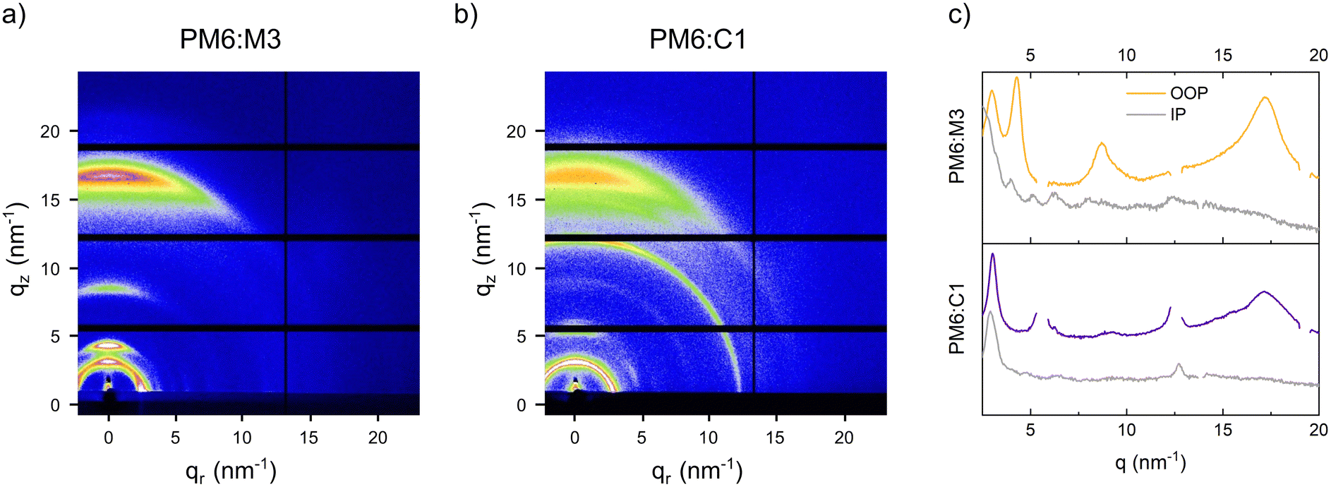 | ||
| Fig. 6 2D GIWAXS images of (a) PM6:M3, (b) PM6:C1 bulk heterojunction films and (c) the corresponding line-cuts in out-of-plane (colored) and in-plane (grey) direction. | ||
Furthermore, when comparing the widths of the lamellar stacking peaks of both samples at 3.0 nm−1 in out-of-plane direction (Fig. 6c), we observe that it is smaller in the PM6:C1 sample, which indicates an increased crystalline coherence length and matches well with the slightly coarser phase separation in the PM6:C1 blend found in the AFM phase images (Fig. 5d). In addition, the extension of the pronounced out-of-plane feature at around 12.5 nm−1 to the in-plane direction reveals a lower degree of preferred face-on orientation in the PM6:C1 sample compared to the PM6:M3 blends. This is also supported by the fact that the lamellar stacking peak at 3.0 nm−1 in the PM6:C1 sample (Fig. 6b) is visible as a semicircle with almost constant radial intensity distribution.
Conclusion
In summary, we synthesized a mono-brominated M3 derivative (C1) and studied the correlations of electrochemical, optical and structural material properties with their photovoltaic performance in comparison to the M3 non-fullerene acceptor. Moreover, a second acceptor with the same BDTPT core and non-halogenated rhodanine-based end groups was synthesized (C2), which showed significantly upshifted energy levels being non-beneficial for their application in organic solar cells in combination with conventionally used high efficiency conjugated donor polymers. Solar cells with PM6:C1 absorber layer blends reached efficiencies up to 11.6%, with a higher open-circuit voltage of 0.914 V compared to PM6:M3 based solar cells (0.894 V) due to the upshifted LUMO level of C1. PM6:M3 and PM6:C1 based devices showed equally high exciton dissociation probability, but the PM6:C1 sample exhibited lower charge collection efficiency with respect to the reference system PM6:M3. Moreover, AFM phase images revealed a coarser phase separation for the C1 based blend films. In future research, we plan to polymerize the herein presented mono-brominated molecule C1 and to investigate its properties in all-polymer organic solar cells. Polymerizing the acceptor bears a further possibility of tuning the donor/acceptor phase separation by the molecular weight of the acceptor, and additionally an easy processability, also in large scale, as well as a good stability of the absorber layer morphology are expected.Experimental methods
The experimental procedures of the materials synthesis and details regarding their characterization are included in the ESI.†The solar cells analyzed in this work were built in the conventional architecture ITO|PEDOT:PSS|donor:acceptor|PNDIT-F3N-Br|Ag. For this, ITO pre-patterned glass substrates (15 × 15 × 1.1 mm3, 15 Ω □−1, Lumtec) were wiped with distilled water and acetone. They were then kept for 60 minutes in an ultrasonic bath at 40 °C and dried with a N2 flow. The PEDOT:PSS (Clevios 4083, Heraeus) hole transport layer (HTL) was spin coated onto the glass/ITO substrates (after oxygen plasma treatment at 99 W for 3 minutes) at 3500 rpm for 40 s and annealed in inert atmosphere at 150 °C for 15 minutes.
All the solutions for the photoactive layers were prepared in chloroform (purity: 99.5%) and 0.5% (v%) 1-chloronaphthalene (total concentration: 13 mg ml−1). They were stirred for 3 hours at 50 °C and overnight without heat. The NFAs M3 and C1 were blended with the polymeric donor PM6 in a D:A weight ratio of 1:1, while the acceptor C2 was blended with the donor PBDB-T, also in a 1:1 weight ratio. Each substrate was coated with 90 μl of solution at 5000 rpm for 45 s, then all the substrates were thermally annealed at 90 °C for 5 minutes.
For the ETL solution, the PNDIT-F3N-Br polymer was dissolved in methanol with a concentration of 0.5 mg ml−1 and stirred overnight. The ETL was deposited on top of the active layer by spin coating 50 μl of solution per substrate at 2000 rpm for 30 s. Lastly, 100 nm of silver were deposited via thermal evaporation onto the substrates at high vacuum (<10−5 mbar) with a rate of 1 Å s−1. The fabricated solar cells had an active area of 9 mm2.
Author contributions
E. Z.: investigation (physical characterization, solar cell characterization, morphological characterization), data curation, formal analysis, methodology, visualization, writing – original draft, writing – review & editing. S. M.: conceptualization, formal analysis, investigation (synthesis, structural analysis), writing – original draft, writing – review & editing. L.-M. H.: investigation (synthesis, physical characterization, solar cell characterization), data analysis, writing – review & editing. H. A.: investigation (GIWAXS), data analysis, resources, writing – review & editing. T. R.: conceptualization, funding acquisition, data analysis, writing – original draft, writing – review & editing. G. T.: conceptualization, funding acquisition, supervision, resources, project administration, writing – review & editing.Conflicts of interest
There are no conflicts of interest to declare.Acknowledgements
The CERIC-ERIC consortium is gratefully acknowledged for the access to experimental facilities (Austrian SAXS beamline at Elettra Sincrotrone Trieste) and financial support. Moreover, the authors acknowledge the use of the Somapp Lab, a core facility supported by the Austrian Federal Ministry of Education, Science and Research, the Graz University of Technology, the University of Graz and Anton Paar GmbH. In addition, the authors thank Karin Bartl, Bettina Schlemmer and Marco Sigl for their experimental support.References
- G. Zhang, F. R. Lin, F. Qi, T. Heumüller, A. Distler, H.-J. Egelhaaf, N. Li, P. C. Y. Chow, C. J. Brabec, A. K.-Y. Jen and H.-L. Yip, Renewed Prospects for Organic Photovoltaics, Chem. Rev., 2022, 122, 14180–14274 CrossRef CAS PubMed.
- B. Schweda, M. Reinfelds, P. Hofstadler, G. Trimmel and T. Rath, Recent Progress in the Design of Fused-Ring Non-Fullerene Acceptors - Relations between Molecular Structure and Optical, Electronic, and Photovoltaic Properties, ACS Appl. Energy Mater., 2021, 4, 11899–11981 CrossRef CAS PubMed.
- L. Zhu, M. Zhang, J. Xu, C. Li, J. Yan, G. Zhou, W. Zhong, T. Hao, J. Song, X. Xue, Z. Zhou, R. Zeng, H. Zhu, C.-C. Chen, R. C. I. MacKenzie, Y. Zou, J. Nelson, Y. Zhang, Y. Sun and F. Liu, Single-Junction Organic Solar Cells with over 19% Efficiency Enabled by a Refined Double-Fibril Network Morphology, Nat. Mater., 2022, 21, 656–663 CrossRef CAS PubMed.
- M. Zhou, C. Liao, Y. Duan, X. Xu, L. Yu, R. Li and Q. Peng, 19.10% Efficiency and 80.5% Fill Factor Layer-by-Layer Organic Solar Cells Realized by 4-Bis(2-Thienyl)Pyrrole-2,5-Dione Based Polymer Additives for Inducing Vertical Segregation Morphology, Adv. Mater., 2023, 35, 2208279 CrossRef CAS PubMed.
- J. Yuan, Y. Zhang, L. Zhou, G. Zhang, H.-L. Yip, T.-K. Lau, X. Lu, C. Zhu, H. Peng, P. A. Johnson, M. Leclerc, Y. Cao, J. Ulanski, Y. Li and Y. Zou, Single-Junction Organic Solar Cell with over 15% Efficiency Using Fused-Ring Acceptor with Electron-Deficient Core, Joule, 2019, 3, 1140–1151 CrossRef CAS.
- W. Liu, X. Xu, J. Yuan, M. Leclerc, Y. Zou and Y. Li, Low-Bandgap Non-fullerene Acceptors Enabling High-Performance Organic Solar Cells, ACS Energy Lett., 2021, 6, 598–608 CrossRef CAS.
- D. Luo, X. Lai, N. Zheng, C. Duan, Z. Wang, K. Wang and A. K. K. Kyaw, High-Performance and Low-Energy Loss Organic Solar Cells with Non-Fused Ring Acceptor by Alkyl Chain Engineering, Chem. Eng. J., 2021, 420, 129768 CrossRef CAS.
- D. Luo, Z. Jiang, W. Yang, X. Guo, X. Li, E. Zhou, G. Li, L. Li, C. Duan, C. Shan, Z. Wang, Y. Li, B. Xu and A. K. K. Kyaw, Dual-Functional Ambipolar Non-Fused Ring Electron Acceptor as Third Component and Designing Similar Molecular Structure between Two Acceptors for High-Performance Ternary Organic Solar Cells, Nano Energy, 2022, 98, 107186 CrossRef CAS.
- F. Zhao, H. Zhang, R. Zhang, J. Yuan, D. He, Y. Zou and F. Gao, Emerging Approaches in Enhancing the Efficiency and Stability in Non-Fullerene Organic Solar Cells, Adv. Energy Mater., 2020, 10, 2002746 CrossRef CAS.
- J. Hou, O. Inganäs, R. H. Friend and F. Gao, Organic Solar Cells Based on Non-Fullerene Acceptors, Nat. Mater., 2018, 17, 119–128 CrossRef CAS PubMed.
- G. Zhang, J. Zhao, P. C. Y. Chow, K. Jiang, J. Zhang, Z. Zhu, J. Zhang, F. Huang and H. Yan, Nonfullerene Acceptor Molecules for Bulk Heterojunction Organic Solar Cells, Chem. Rev., 2018, 118, 3447–3507 CrossRef CAS PubMed.
- C. Li, J. Zhou, J. Song, J. Xu, H. Zhang, X. Zhang, J. Guo, L. Zhu, D. Wei, G. Han, J. Min, Y. Zhang, Z. Xie, Y. Yi, H. Yan, F. Gao, F. Liu and Y. Sun, Non-Fullerene Acceptors with Branched Side Chains and Improved Molecular Packing to Exceed 18% Efficiency in Organic Solar Cells, Nat. Energy, 2021, 6, 605–613 CrossRef CAS.
- Y. Cui, H. Yao, J. Zhang, K. Xian, T. Zhang, L. Hong, Y. Wang, Y. Xu, K. Ma, C. An, C. He, Z. Wei, F. Gao and J. Hou, Single-Junction Organic Photovoltaic Cells with Approaching 18% Efficiency, Adv. Mater., 2020, 32, 1908205 CrossRef CAS PubMed.
- X. Zhao, Q. An, H. Zhang, C. Yang, A. Mahmood, M. Jiang, M. H. Jee, B. Fu, S. Tian, H. Y. Woo, Y. Wang and J.-L. Wang, Double Asymmetric Core Optimizes Crystal Packing to Enable Selenophene-based Acceptor with over 18% Efficiency in Binary Organic Solar Cells, Angew. Chem., Int. Ed., 2023, 62, e202216340 CrossRef CAS PubMed.
- C. Yang, Q. An, H.-R. Bai, H.-F. Zhi, H. S. Ryu, A. Mahmood, X. Zhao, S. Zhang, H. Y. Woo and J.-L. Wang, A Synergistic Strategy of Manipulating the Number of Selenophene Units and Dissymmetric Central Core of Small Molecular Acceptors Enables Polymer Solar Cells with 17.5% Efficiency, Angew. Chem., Int. Ed., 2021, 60, 19241 CrossRef CAS PubMed.
- H. Yao, J. Wang, Y. Xu and J. Hou, Terminal Groups of Nonfullerene Acceptors: Design and Application, Chem. Mater., 2023, 35, 807–821 CrossRef CAS.
- A. Tang, B. Xiao, Y. Wang, F. Gao, K. Tajima, H. Bin, Z. I.-G. Zhang, Y. Li, Z. Wie and E. Zhou, Simultaneously Achieved High Open-Circuit Voltage and Efficient Charge Generation by Fine-Tuning Charge-Transfer Driving Force in Nonfullerene Polymer Solar Cells, Adv. Funct. Mater., 2018, 28, 1704507 CrossRef.
- Q. Zhang, B. Kan, F. Liu, G. Long, X. Wan, X. Chen, Y. Zuo, W. Ni, H. Zhang, M. Li, Z. Hu, F. Huang, Y. Cao, Z. Liang, M. Zhang, T. P. Russell and Y. Chen, Small-Molecule Solar Cells with Efficiency over 9%, Nat. Photonics, 2015, 9, 35–41 CrossRef CAS.
- S. Holliday, R. S. Ashraf, A. Wadsworth, D. Baran, S. A. Yousaf, C. B. Nielsen, C.-H. Tan, S. D. Dimitrov, Z. Shang, N. Gasparini, M. Alamoudi, F. Laquai, C. J. Brabec, A. Salleo, J. R. Durrant and I. McCulloch, High-Efficiency and Air-Stable P3HT-Based Polymer Solar Cells with a New Non-Fullerene Acceptor, Nat. Commun., 2016, 7, 11585 CrossRef CAS PubMed.
- Y. Zhang, G. Cai, Y. Li, Z. Zhang, T. Li, X. Zuo, X. Lu and Y. Lin, An Electron Acceptor Analogue for Lowering Trap Density in Organic Solar Cells, Adv. Mater., 2021, 33, 2008134 CrossRef CAS PubMed.
- W. Zhao, S. Li, H. Yao, S. Zhang, Y. Zhang, B. Yang and J. Hou, Molecular Optimization Enables over 13% Efficiency in Organic Solar Cells, J. Am. Chem. Soc., 2017, 139, 7148–7151 CrossRef CAS PubMed.
- C. Li, J. Zhou, J. Song, J. Xu, H. Zhang, X. Zhang, J. Guo, L. Zhu, D. Wei, G. Han, J. Min, Y. Zhang, Z. Xie, Y. Yi, H. Yan, F. Gao, F. Liu and Y. Sun, Non-Fullerene Acceptors with Branched Side Chains and Improved Molecular Packing to Exceed 18% Efficiency in Organic Solar Cells, Nat. Energy, 2021, 6, 605–613 CrossRef CAS.
- Y. Zhang, H. Yao, S. Zhang, Y. Qin, J. Zhang, W. Li, Z. Wei, F. Gao and J. Hou, Fluorination vs. Chlorination: A Case Study on High Performance Organic Photovoltaic Materials, Sci. China Chem., 2018, 61, 1328–1337 CrossRef CAS.
- X. Li, I. Angunawela, Y. Chang, J. Zhou, H. Huang, L. Zhong, A. Liebman-Pelaez, C. Zhu, L. Meng, Z. Xie, H. Ade, H. Yan and Y. Li, Effect of the Chlorine Substitution Position of the End-Group on Intermolecular Interactions and Photovoltaic Performance of Small Molecule Acceptors, Energy Environ. Sci., 2020, 13, 5028–5038 RSC.
- C. He, Y. Pan, Y. Ouyang, Q. Shen, Y. Gao, K. Yan, J. Fang, Y. Chen, C.-Q. Ma, J. Min, C. Zhang, L. Zuo and H. Chen, Manipulating the D:A Interfacial Energetics and Intermolecular Packing for 19.2% Efficiency Organic Photovoltaics, Energy Environ. Sci., 2022, 15, 2537–2544 RSC.
- D. Deng, Y. Zhang, J. Zhang, Z. Wang, L. Zhu, J. Fang, B. Xia, Z. Wang, K. Lu, W. Ma and Z. Wei, Fluorination-Enabled Optimal Morphology Leads to over 11% Efficiency for Inverted Small-Molecule Organic Solar Cells, Nat. Commun., 2016, 7, 13740 CrossRef CAS PubMed.
- X. Zhang, G. Li, S. Mukherjee, W. Huang, D. Zheng, L.-W. Feng, Y. Chen, J. Wu, V. K. Sangwan, M. C. Hersam, D. M. DeLongchamp, J. Yu, A. Facchetti and T. J. Marks, Systematically Controlling Acceptor Fluorination Optimizes Hierarchical Morphology, Vertical Phase Separation, and Efficiency in Non-Fullerene Organic Solar Cells, Adv. Energy Mater., 2022, 12, 2102172 CrossRef CAS.
- W. Li, L. Ye, S. Li, H. Yao, H. Ade and J. Hou, A High-Efficiency Organic Solar Cell Enabled by the Strong Intramolecular Electron Push–Pull Effect of the Nonfullerene Acceptor, Adv. Mater., 2018, 30, 1707170 CrossRef PubMed.
- H. Zhang, H. Yao, J. Hou, J. Zhu, J. Zhang, W. Li, R. Yu, B. Gao, S. Zhang and J. Hou, Over 14% Efficiency in Organic Solar Cells Enabled by Chlorinated Nonfullerene Small-Molecule Acceptors, Adv. Mater., 2018, 30, 1800613 CrossRef PubMed.
- D. Luo, Z. Jiang, C. Shan, L. Li, C. Duan, Q. Liu, Z. Wang, K. Wang, B. Xu and A. K. K. Kyaw, Simultaneous Tuning of Alkyl Chains and End Groups in Non-fused Ring Electron Acceptors for Efficient and Stable Organic Solar Cells, ACS Appl. Mater. Interfaces, 2022, 14, 24374–24385 CrossRef CAS PubMed.
- Q. Zhao, J. Qu and F. He, Chlorination: An Effective Strategy for High-Performance Organic Solar Cells, Adv. Sci., 2020, 7, 2000509 CrossRef CAS PubMed.
- H. Yao, J. Wang, Y. Xu, S. Zhang and J. Hou, Recent Progress in Chlorinated Organic Photovoltaic Materials, Acc. Chem. Res., 2020, 53, 822–832 CrossRef CAS PubMed.
- D. Luo, L. Zhang, J. Zeng, W. Chi, J. Zhou, E. Zhou, L. Li, T. Iwahashi, T. Michinobu, Y. Ouchi, B. Xu and A. K. K. Kyaw, Revealing the Effect of Halogenation Strategy on the Regulation of Crystallization Kinetics and Molecular Packing for High-Performance Organic Solar Cells, Adv. Funct. Mater., 2023, 2311736 CrossRef.
- Y. Cui, H. Yao, J. Zhang, T. Zhang, Y. Wang, L. Hong, K. Xian, B. Xu, S. Zhang, J. Peng, Z. Wei, F. Gao and J. Hou, Over 16% Efficiency Organic Photovoltaic Cells Enabled by a Chlorinated Acceptor with Increased Open-Circuit Voltages, Nat. Commun., 2019, 10, 2515 CrossRef PubMed.
- Y. Chen, R. Ma, T. Liu, Y. Xiao, H. K. Kim, J. Zhang, C. Ma, H. Sun, F. Bai, X. Guo, K. S. Wong, X. Lu and H. Yan, Side-Chain Engineering on Y-Series Acceptors with Chlorinated End Groups Enables High-Performance Organic Solar Cells, Adv. Energy Mater., 2021, 11, 2003777 CrossRef CAS.
- Y. Zou, H. Chen, X. Bi, X. Xu, H. Wang, M. Lin, Z. Ma, M. Zhang, C. Li, X. Wan, G. Long, Y. Zhaoyang and Y. Chen, Peripheral Halogenation Engineering Controls Molecular Stacking to Enable Highly Efficient Organic Solar Cells, Energy Environ. Sci., 2022, 15, 3519–3533 RSC.
- A. Romo-Gutiérrez, Z. N. Cisneros-García and J. G. Rodríguez-Zavala, Improvement of Photovoltaic Related Parameters Through Bromination and the Role of Chlorine, Bromine, Iodine, and Dehalogenation in the Fluorinated Y6 Small Molecule, Mol. Phys., 2022, 120, e2135466 CrossRef.
- H. Wang, T. Liu, J. Zhou, D. Mo, L. Han, H. Lai, H. Chen, N. Zheng, Y. Zhu, Z. Xie and F. He, Bromination: An Alternative Strategy for Non-Fullerene Small Molecule Acceptors, Adv. Sci., 2020, 7, 1903784 CrossRef CAS PubMed.
- S.-S. Wan, C. Chang, J.-L. Wang, G.-Z. Yuan, Q. Wu, M. Zhang and Y. Li, Effects of the Number of Bromine Substitution on Photovoltaic Efficiency and Energy Loss of Benzo[1,2-b:4,5-b]diselenophene-based Narrow-Bandgap Multibrominated Nonfullerene Acceptors, Sol. RRL, 2019, 3, 1800250 CrossRef.
- Y. Liu, Y. Zhao, S. Lu, K. Zhu, Q. Wang, X. Kang, L. Yu, S. Dai and M. Sun, Effects of Brominated Terminal Groups on the Performance of Fused-Ring Electron Acceptors in Organic Solar Cells, Dyes Pigm., 2021, 194, 109652 CrossRef CAS.
- L. Wang, Q. An, L. Yan, H.-R. Bai, M. Jiang, A. Mahmood, C. Yang, H. Zhia and J.-L. Wang, Non-Fullerene Acceptors with Hetero-Dihalogenated Terminals Induce Significant Difference in Single Crystallography and Enable Binary Organic Solar Cells with 17.5% Efficiency, Energy Environ. Sci., 2022, 15, 320–333 RSC.
- L. Yan, H. Zhang, Q. An, M. Jiang, A. Mahmood, M. H. Jee, H.-R. Bai, H.-F. Zhi, S. Zhang, H. Y. Woo and J.-L. Wang, Regioisomer-Free Difluoro-Monochloro Terminal-based Hexa-Halogenated Acceptor with Optimized Crystal Packing for Efficient Binary Organic Solar Cells, Angew. Chem., Int. Ed., 2022, 61, e202209454 CrossRef CAS PubMed.
- Q. Yang, D. Hu, M. Kumar, H. Dong, S. Ahmed, P. Huang, Z. Xiao and S. Lu, Effects of Mixed Halogenation on the Performance of Nonfullerene Acceptors in All-Small Molecule Organic Solar Cells, Sol. RRL, 2023, 7, 2201062 CrossRef CAS.
- H. Yu, Y. Wang, X. Zou, H. Han, H. K. Kim, Z. Yao, Z. Wang, Y. Li, H. M. Ng, W. Zhou, J. Zhang, S. Chen, X. Lu, K. S. Wong, Z. Zhu, H. Yan and H. Hu, Effects of Halogenation of Small-Molecule and Polymeric Acceptors for Efficient Organic Solar Cells, Adv. Funct. Mater., 2023, 33, 2300712 CrossRef CAS.
- D. Mo, H. Chen, Y. Zhu, H.-H. Huang, P. Chao and F. He, Effects of Halogenated End Groups on the Performance of Nonfullerene Acceptors, ACS Appl. Mater. Interfaces, 2021, 13, 6147–6155 CrossRef CAS PubMed.
- C. Zhang, T. Liu, J.-L. Wang, K.-K. Liu, C. Yang, H.-J. Zhang, R. Ma and H. Yan, Tetrabromination versus Tetrachlorination: A Molecular Terminal Engineering of Nonfluorinated Acceptors to Control Aggregation for Highly Efficient Polymer Solar Cells with Increased Voc and Higher Jsc Simultaneously, Sol. RRL, 2020, 4, 2000212 CrossRef CAS.
- F. Yang, C. Li, W. Lai, A. Zhang, H. Huang and W. Li, Halogenated Conjugated Molecules for Ambipolar Field-Effect Transistors and Non-Fullerene Organic Solar Cells, Mater. Chem. Front., 2017, 1, 1389–1395 RSC.
- J. Jia, Q. Huang, T. Jia, K. Zhang, J. Zhang, J. Miao, F. Huang and C. Yang, Fine-Tuning Batch Factors of Polymer Acceptors Enables a Binary All-Polymer Solar Cell with High Efficiency of 16.11%, Adv. Energy Mater., 2022, 12, 2103193 CrossRef CAS.
- H. Fu, Y. Li, Z. Wu, F. R. Lin, H. Y. Woo and A. K.-Y. Jen, Side-Chain Substituents on Benzotriazole-Based Polymer Acceptors Affecting the Performance of All-Polymer Solar Cells, Macromol. Rapid Commun., 2022, 43, 2200062 CrossRef CAS PubMed.
- Y. Ma, M. Zhang, S. Wan, P. Yin, P. Wang, D. Cai, F. Liu and Q. Zheng, Efficient Organic Solar Cells from Molecular Orientation Control of M-Series Acceptors, Joule, 2021, 5, 197–209 CrossRef CAS.
- Y. Ma, D. Cai, S. Wan, P. Yin, P. Wang, W. Lin and Q. Zheng, Control over π–π Stacking of Heteroheptacene-Based Nonfullerene Acceptors for 16% Efficiency Polymer Solar Cells, Natl. Sci. Rev., 2020, 7, 1886–1895 CrossRef CAS PubMed.
- Y. Ma, R. Sun, Z. Chen, S. Zhang, D. Cai, S. Wan, W. Lin, S.-Q. Zhang, Q. Tu, W. Ma, J. Min, X. Hao and Q. Zheng, 17% Efficiency for Linear-Shaped ADA-Type Nonfullerene Acceptors Enabled by 3D Reticulated Molecular Packing, Nano Energy, 2023, 107, 108116 CrossRef CAS.
- S. Wan, Y. Ma, D. Cai, W. Lin, P. Wang, J. Wang and Q. Zheng, Enhancing the Photovoltaic Performance of Ladder-Type Heteroheptacene-based Nonfullerene Acceptors by Incorporating Halogen Atoms on Their Ending Groups, Adv. Funct. Mater., 2021, 31, 2010436 CrossRef CAS.
- S. Liu, J. Yuan, W. Deng, M. Luo, Y. Xie, Q. Liang, Y. Zou, Z. He, H. Wu and Y. Cao, High-Efficiency Organic Solar Cells with Low Non-Radiative Recombination Loss and Low Energetic Disorder, Nat. Photonics, 2020, 14, 300–305 CrossRef CAS.
- Y. Cai, H. Zhang, L. Ye, R. Zhang, J. Xu, K. Zhang, P. Bi, T. Li, K. Weng, K. Xu, J. Xia, Q. Bao, F. Liu, X. Hao, S. Tan, F. Gao, X. Zhan and Y. Sun, Effect of the Energy Offset on the Charge Dynamics in Nonfullerene Organic Solar Cells, ACS Appl. Mater. Interfaces, 2020, 12, 43984–43991 CrossRef CAS PubMed.
- S. Li, L. Zhan, C. Sun, H. Zhu, G. Zhou, W. Yang, M. Shi, C.-Z. Li, J. Hou, Y. Li and H. Chen, Highly Efficient Fullerene-Free Organic Solar Cells Operate at Near Zero Highest Occupied Molecular Orbital Offsets, J. Am. Chem. Soc., 2019, 141, 3073–3082 CrossRef CAS PubMed.
- P. Fürk, S. Mallick, T. Rath, M. Reinfelds, M. Wu, E. Spiecker, N. Simic, G. Haberfehlner, G. Kothleitner, B. Ressel, S. Holler, J. B. Schaubeder, P. Materna, H. Amenitsch and G. Trimmel, The Challenge with High Permittivity Acceptors in Organic Solar Cells: A Case Study with Y-Series Derivatives, J. Mater. Chem. C, 2023, 11, 8393–8404 RSC.
- J. Lv, H. Tang, J. Huang, C. Yan, K. Liu, Q. Yang, D. Hu, R. Singh, J. Lee, S. Lu, G. Li and Z. Kann, Additive-Induced Miscibility Regulation and Hierarchical Morphology Enable 17.5% Binary Organic Solar Cells, Energy Environ. Sci., 2021, 14, 3044–3052 RSC.
Footnote |
| † Electronic supplementary information (ESI) available. See DOI: https://doi.org/10.1039/d3nj05560d |
| This journal is © The Royal Society of Chemistry and the Centre National de la Recherche Scientifique 2024 |