DOI:
10.1039/D4NH00245H
(Communication)
Nanoscale Horiz., 2024,
9, 1557-1567
Mechanical regulation to interfacial thermal transport in GaN/diamond heterostructures for thermal switch†
Received
30th May 2024
, Accepted 5th July 2024
First published on 8th July 2024
Abstract
Gallium nitride offers an ideal material platform for next-generation high-power electronics devices, which enable a spectrum of applications. The thermal management of the ever-growing power density has become a major bottleneck in the performance, reliability, and lifetime of the devices. GaN/diamond heterostructures are usually adopted to facilitate heat dissipation, given the extraordinary thermal conduction properties of diamonds. However, thermal transport is limited by the interfacial conductance at the material interface between GaN and diamond, which is associated with significant mechanical stress at the atomic level. In this work, we investigate the effect of mechanical strain perpendicular to the GaN/diamond interface on the interfacial thermal conductance of heterostructures using full-atom non-equilibrium molecular dynamics simulations. We found that the heterostructure exhibits severe mechanical stress at the interface in the absence of loading, which is due to lattice mismatch. Upon tensile/compressive loading, the interfacial stress is more pronounced, and the strain is not identical across the interface owing to the contrasting elastic moduli of GaN and diamond. In addition, the interfacial thermal conductance can be notably enhanced and suppressed by tensile and compressive strains, respectively, leading to a 400% variation in thermal conductance. More detailed analyses reveal that the change in interfacial thermal conductance is related to the surface roughness and interfacial bonding strength, as described by a generalized relationship. Moreover, phonon analyses suggest that the unequal mechanical deformation under compressive strain in GaN and diamond induces different frequency shifts in the phonon spectra, leading to an enhancement in phonon overlapping energy, which promotes phonon transport at the interface and elevates the thermal conductance and vice versa for tensile strain. The effect of strain on interface thermal conductance was investigated at various temperatures. Based on the mechanical tunability of thermal conductance, we propose a conceptual design for a mechanical thermal switch that regulates thermal conductance with excellent sensitivity and high responsiveness. This study offers a fundamental understanding of how mechanical strain can adjust interface thermal conductance in GaN/diamond heterostructures with respect to mechanical stress, deformation, and phonon properties. These results and findings lay the theoretical foundation for designing thermal management devices in a strain environment and shed light on developing intelligent thermal devices by leveraging the interplay between mechanics and thermal transport.
New concepts
GaN/diamond heterostructures exhibit superb transport properties that have enormous potential to improve the thermal management of high-power electronic devices. However, the thermal transport performance is limited by the thermal conductance at the interface between GaN and diamond, which is associated with significant interfacial mechanical stress at the atomic level. Using full-scale molecular dynamics simulations, we report that the thermal boundary conductance of a GaN/diamond heterostructure with ±5% external mechanical loading can achieve 400% variation without damaging the interface. The external mechanical loading can notably alter the thermal boundary conductance due to the mechanically tunable interface morphology and phonon resonance. Furthermore, a general regulation law between the thermal boundary conductance and the overall surface roughness with various strain states is, for the first time, established to quantitatively describe the interfacial thermal transport of GaN/diamond heterostructures in a mechanical strain environment. A conceptual design of a “mechanical thermal switch” is proposed, which effectively regulates the heat flux across the interface under external tensile and compressive loading. These results and findings lay the theoretical foundation for designing thermal management devices in a strain environment and shed light on developing intelligent thermal devices by leveraging the interplay between mechanics and thermal transport.
|
Introduction
As one of the most promising materials for the 3rd-generation semiconductors,1,2 gallium nitride (GaN) exhibits a collection of unique electronics properties, including high electron mobility,3,4 low losses,5,6 high breakdown voltage,7 high saturation drain current,8 low on-resistance,9,10 and a wide direct bandgap of ∼3.4 eV, which lead to broad applications in high-performance electronic devices like solar inverters, AC–DC power rectifiers, and power amplifiers.11,12 However, the evergrowing power density in GaN devices is associated with an elevated heat flux density beyond 300 kW cm−2,13,14 which causes enormous temperature rise and unwanted emergence of hot spots in the device,15,16 limiting the performance and reliability of the device.17,18 Therefore, efficient thermal management is of critical importance in the development of future electronic devices.
The intrinsic thermal conductivity of GaN, 200 W m K−1, is limited compared to those of other 3rd-generation semiconductor materials like SiC, AlN, and ZnO, imposing enormous challenges on heat dissipation.3,19 Diamond possesses the highest thermal conductivity among all natural materials, making it an excellent heat dissipation substrate. GaN devices fabricated using a diamond substrate exhibit the highest maximum drain current and the lowest surface temperature.20 Therefore, GaN/diamond heterostructures are widely utilized in the thermal management of high-power and high-frequency electronic devices.21–23 Due to the severe lattice mismatch ratio between GaN and diamond, as well as the crystal structure changes and surface morphology differences caused by defects and surface roughness, they are usually bonded with a transition/adhesion layer to the interface.20,24,25 However, the presence of an intermediate layer introduces two additional interfaces with enhanced phonon boundary scattering, which suppresses the overall thermal boundary conductance (TBC).26,27 In contrast, the surface activation bonding method can produce GaN/diamond heterostructures with covalent bonding interfaces, leading to improved TBC.28,29 Nonetheless, this method cannot avoid the interfacial stresses introduced by the apparent difference in the lattice constants between the two species.30 In addition, due to the difference in the coefficient of thermal expansion between diamond and GaN, interfacial thermal stress is inevitably induced during the manufacturing process.31–33 At the nanoscale, the thermal transport properties of heterostructures are very sensitive to internal or external mechanical effects.34–39 The interfacial stresses, defects, and surface roughness that affect interface morphology and quality become the main factors limiting TBC. Typically, defects and high surface roughness change the interfacial crystal structure and surface morphology, reduce the interface bonding strength, and intensify phonon localization, leading to enhanced phonon scattering at the interface, thereby decreasing the TBC.40,41 The presence of defects and high surface roughness is expected to introduce additional interfacial stresses compared to the state without both. These factors have the potential to further influence the interplay between the mechanics and thermal transport. However, the correlation between the TBC and interfacial stress remains unexplored for the GaN/diamond heterostructures, which is essential for the thermal management of GaN-based devices.
In the present work, using full-atom nonequilibrium molecular dynamics (MD) simulations, we elucidate that the TBC of GaN/diamond heterostructures is highly sensitive to tensile/compressive strain perpendicular to the interface. A ±5% strain can induce a 400% variation in the TBC without damaging the interface. Such mechanical tunability is closely related to the behavior of stress and interface morphology. Analysis of the stress distribution of the GaN/diamond heterostructures reveals that the lattice mismatch induces interfacial stress at the 20 GPa level. Upon strain loading, a significant stress concentration occurs at the interface, which remains until the failure/collapse. Compressive/tensile strain can generally decrease/increase the surface roughness, thereby improving/suppressing the interfacial interaction, which enhances/reduces the TBC. A general regulation law can be established between the TBC and the surface roughness at various stress states. In addition, the compressive loading causes unequal deformation in GaN and diamond, which increases the phonon overlap energy and enhances the TBC. The efficacy of compressive strain in improving the TBC is further validated at various temperatures. Based on the mechanical tunability of TBC, we propose a conceptual design for a mechanical thermal switch with further MD simulations. The mechanical thermal switch can regulate interfacial thermal transport with its adjustable TBC. With a prescribed heat flux, the thermal switch can achieve a 400-K variation in the temperature drop between the hot and cold ends. This work provides numerical insight into the cooling of GaN-based electronic devices in mechanical environments. The thermal–mechanics coupling mechanisms explored in the current study lay the theoretical foundation for developing intelligent thermal devices by leveraging the interplay between mechanics and thermal transport.
Results and discussion
Stress induced by internal lattice mismatch and external loading
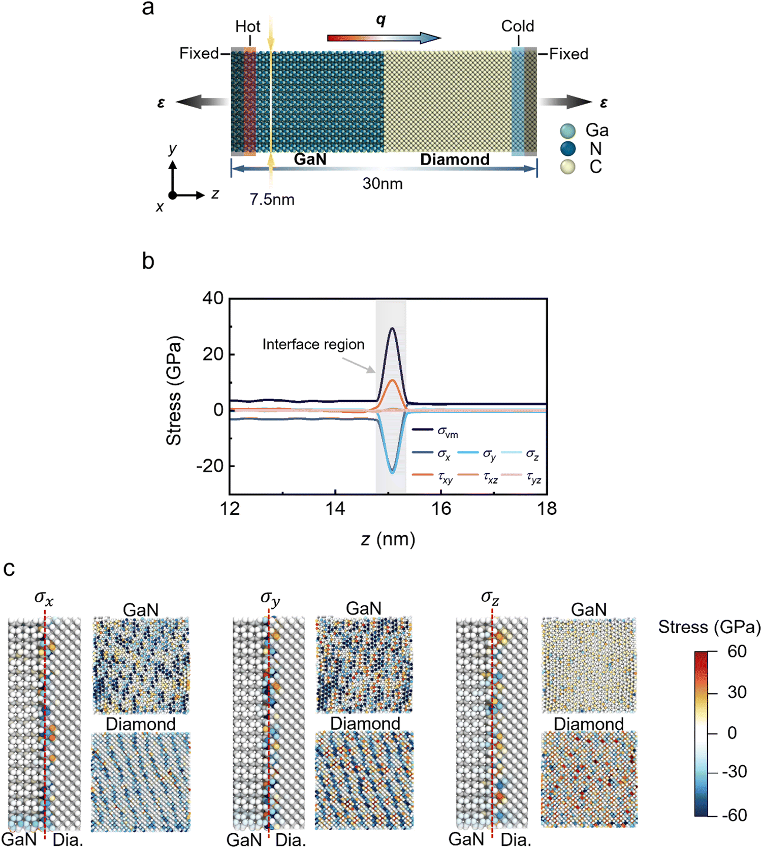
Fig. 1b presents the one-dimensional distribution of multiple stress components in the absence of external mechanical loading (ε = 0%), where σx, σy and σz represent the normal stresses, τxy, τxz, and τyz represent the shear stresses, and σvm is the von Mises stress. The stress components maintain a relatively low level in both GaN and diamond away from the interface while significant peaks in σx, σy and τxy emerge at the interface, which are parallel to the interface of the heterostructure. Fig. 1c displays the y–z and x–y planar distribution of atomic stresses σx, σy and σz at the interface between GaN and diamond. The atomic stress is more pronounced in GaN than in diamond, indicating that the peaks in the stress profile are predominantly contributed by GaN rather than diamond. The contrasting stress levels in the two constituents of the heterostructures are due to the fact that the elastic modulus of diamond is much higher than that of GaN. The enormous stress at the GaN interface is characterized by periodic patterns and can be attributed to the lattice mismatch between GaN and diamond. The lattice mismatch is quantified by the lattice mismatch ratio λ = (|aDiamond − aGaN|)/aGaN, where aGaN and aDiamond are the lattice constants of GaN and diamond, respectively. The lattice constants of GaN in the x- and y-directions are 3.189 and 5.532 Å, respectively (Fig. S2a and b, ESI†), and the lattice constant of diamond is 3.567 Å (Fig. S2c, ESI†). The lattice mismatch ratios λ in the x and y directions are evaluated as λx = 0.119 and λy = 0.354. Owing to a higher λ in the y-direction, the magnitude of σy is greater than that of σx. In addition, the lattice mismatch in the x–y plane also induces shear stress τxy, as shown in Fig. S3 (ESI†). In contrast, σz, τxz and τyz are not affected by the lattice mismatch, as they are perpendicular to the interface. Based on the distribution of stress on the z-axis, an interface region can be recognized as the location where the stress components in the x–y plane deviate from the values in the bulk region.
 |
| | Fig. 1 Computational model of the GaN/diamond heterostructure and its initial stress distribution. (a) Schematic of the GaN/diamond heterostructure; heat flux is achieved along the z-direction, perpendicular to the interface of the heterostructure, and a uniaxial tensile/compressive strain ε is applied in the z-direction. The ends are set to the fixed regions, and thoseclosest to the fixed region are selected as the hot and cold reservoirs, respectively. (b) The one-dimensional distribution of multiple stress components in the absence of external mechanical loading (ε = 0%). (c) The y–z and x–y planar distributions of atomic stresses σx, σy and σz at the interface between GaN and diamond. | |
Fig. 2a shows the nominal stress–strain (σ–ε) curve of the heterostructure subjected to external tensile loading (gray curve), accompanied by the stress–strain curves of diamond (light blue) and GaN (dark blue) for comparison. For all three materials, the stress σ increases linearly when the nominal strain is less than 3%, followed by a nonlinear monotonic increase until failure. At a specific ε, the σ–ε curve of the heterostructure lies between that of GaN and diamond. By performing linear regression on the σ–ε data within the linear range, the elastic moduli of diamond, GaN, and the heterostructure are 0.976, 0.331, and 0.541 TPa, respectively. The values of the failure strain of diamond and GaN are 16.30% and 22.48%, respectively, indicated by the abrupt drop in the stress values in the σ–ε curves. Surprisingly, the failure strain of the heterostructure is 6.96%, which is lower than those of both bulk materials. The enormous reduction in the failure strain is due to the significant interfacial stress, which contributes to early failure at the interface, as illustrated by the snapshots of the fracture in Fig. S4a (ESI†). Fig. 2b presents the nominal compressive stress–strain curves of the three materials. Under compressive strain, the nominal stress in the bulk diamond exhibits a linear increase with nominal strain. Crushing does not occur for a compressive strain of up to 20%, which has been reported in previous studies,42,43 withstanding larger compressive strains without being crushed. In contrast, bulk GaN exhibits an earlier stress increase and crushing behavior at ε = −8.09%. The interface of the heterostructure could absorb a compressive strain of ∼1% before the increase in compressive stress, resulting in crushing under ε = −11.16%. The snapshots of the crushing behavior at the interface of the heterostructure are shown in Fig. S4b (ESI†).
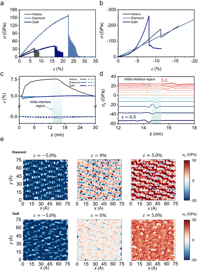 |
| | Fig. 2 Uniaxial nominal stress–strain curves for bulk GaN, bulk diamond and the heterostructure, and strain/stress variation at the interface of the heterostructure. (a) Uniaxial tensile nominal stress–strain curves for the three materials. (b) Uniaxial compression nominal stress–strain curves for the three materials. (c) Strain distribution along the z-direction of bulk GaN, bulk diamond, and the heterostructure under tensile/compressive strain. The solid line represents the tensile strain and the dotted line represents the compressive strain, and the initial interface region represents the interface position of the heterostructure at ε = 0%. (d) The stress σz distribution under different tensile/compressive strains. (e) The magnitude and distribution of atomic stress σz under ε = ±5% and ε = 0% on diamond and GaN at the interface. The red region represents the tensile stress, and the blue region represents the compressive stress. The darker the color, the greater the stress value. | |
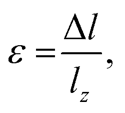
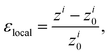
In order to elucidate the deformation mechanism of the heterostructure under tensile/compressive strain, the local strain εlocal of the ith atom in the system was evaluated as
| |  | (1) |
where
zi and
zi0 represent the
z coordinate of the
ith atom with and without external loading, respectively.
Fig. 2c displays the distribution of
εlocal in the heterostructure along the
z-direction at
ε = ±5% (gray curves), which is lower than the strain that leads to failure or crushing. The green-shaded region marks the initial interface region identified by stress distribution (
Fig. 1b). The results for bulk GaN (dark blue) and diamond (light blue) with the same size are also plotted for comparison. For bulk materials, the
εlocal values are almost homogeneous. As for the heterostructure, the compressive strain also leads to a homogeneous distribution of
εlocal, suggesting that the deformations in the GaN and diamond regions are almost identical, which is due to the close stress values and compressive elastic moduli in the GaN and diamond at
ε = −5%.
43,44 In contrast, the homogeneity in
εlocal is broken when the heterostructure is under tensile loading. The maximum value is 7.57% and emerges at the interface to accommodate the external tensile loading, which also indicates that the heterojunction possesses a lower bonding strength than the constituent materials. In addition,
εlocal is generally higher in GaN than in diamond since the elastic modulus of GaN is lower than that of diamond. The unequal deformation in GaN and diamond can also be reflected by the distribution of stress along the
z-direction as shown in
Fig. 2d. The distributions of
σx and
σy are presented in Fig. S5a and b (ESI
†), respectively. The stress distributions with various nominal strain values are characterized by a notable variation close to
z = 15 nm, which is attributed to the stress caused by the lattice mismatch. Under external tensile/compressive loading, unequal deformation in the materials shifts the location of the interface to the right/left. Moreover, the interface experiences more significant stress peaks under a larger tensile/compressive strain compared to the bulk parts, indicating the presence of stress concentration.
Fig. 2e shows the planar distribution of σz in the x–y plane at the interface with various nominal strains of 0, −5%, and 5%. The stress distributions in diamond and GaN are shown in the upper and lower columns, respectively. When ε = 0%, the interfacial stress in diamond is notably higher than that in GaN and exhibits periodic patterns. The patterns are related to the atomic arrangement of the diamond parallel to the interface, where the locations of tensile and compressive stresses are arranged in an alternating fashion. On the contrary, the patterns of the stress distribution in GaN are less ordered. Under tensile or compressive strain, the patterns in the diamond remain, which suggests that the arrangement of carbon atoms at the interface is highly stable against loading due to the outstanding mechanical strength of the diamond. The variations in σx and σy are less significant compared to those in σz, as illustrated by the planar distributions in Figs. S6a and b (ESI†).
Influence of strain on the thermal boundary conductance of the heterostructure
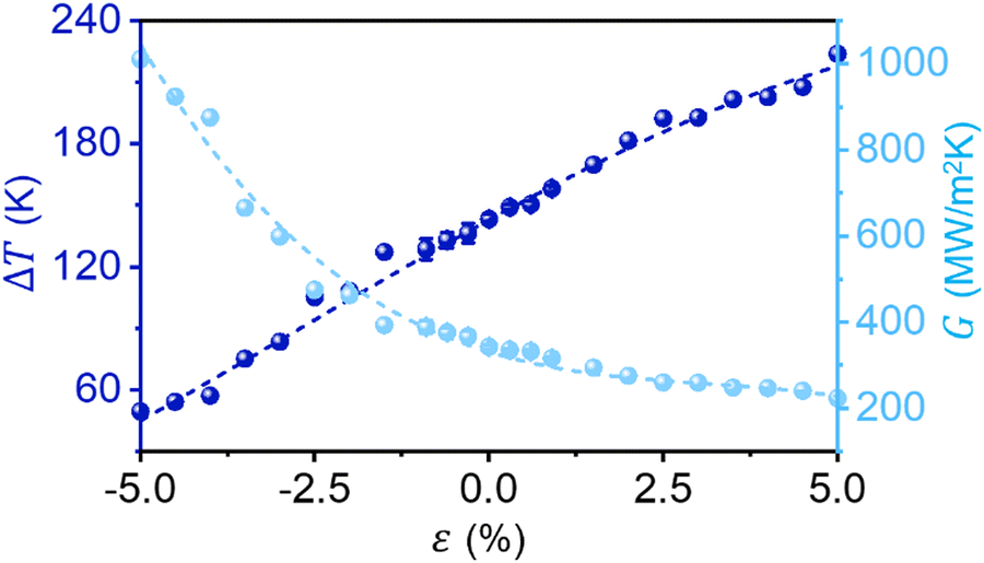
The mechanical loading and the behavior of the stress level also introduce significant variations in G at the interface, as shown in Fig. 3. The calculated TBC values are approximately ∼340 MW m−2 K−1, which is consistent with the TBC data (∼330 MW m−2 K−1) predicted by the diffusion mismatch model (DMM) for GaN/diamond composites at room temperature.14 With a constant heat flux from GaN to diamond across the interface (Fig. 1), the nominal strain of ±5% leads to the variation in G from 223.4 (with 5% tensile strain) to 1010.4 MW m−2 K−1 (with 5% compressive strain), demonstrating a tuning range of nearly ∼400%. Correspondingly, the temperature drop at the interface (ΔT) is altered between 229.66 and 50.77 K. The reduction in the TBC due to tensile strain is less severe with a larger ε and diminishes it at ε = 5%. Conversely, compressive strain results in an increasing trend in TBC. This suggests that the responsiveness of the TBC to compressive strain is higher than that to tensile strain. The different responses of G to tensile and compressive strains are due to the fact that compression generally enhances the atomic interaction as it reduces the separation between atoms; tensile strain increases the separation of atoms and weakens atomic interactions.
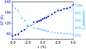 |
| | Fig. 3 Influence of strain on thermal boundary conductance of the heterostructure. The vertical axis on the left is the ΔT at the interface. The vertical axis on the right is the thermal boundary conductance G. | |
To elucidate the mechanical tunability of the TBC, we investigate the surface morphology and roughness Ra of diamond and GaN at the interface of the heterostructure, as shown in Fig. 4. The surface roughness Ra was evaluated using  , where n is the number of atoms at the surface of diamond or GaN at the interface, h is the difference between the z coordinates of the ith atoms at the interface, and hi is the mean value of the z coordinates
  . The atoms in the first layer closest to the interface are employed to calculate Ra; the detailed layering scheme is illustrated in Fig. S7 (ESI†). RaDia and RaGaN represent the surface roughness of the diamond and GaN at the heterostructure interface, respectively. When ε = 0%, RaDia and RaGaN are 0.407 and 0.408 Å, respectively, which are almost identical. Additionally, the peaks in |h| are finer and denser in diamond than in GaN, which can be attributed to the higher elastic modulus of diamond. External tensile/compressive strain enhances/suppresses deformation at the interface, which generally increases/decreases Ra in both GaN and diamond. With a specific value of ε, Ra is systematically lower in diamond than in GaN due to the smaller deformation in diamond.
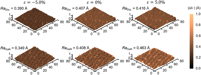 |
| | Fig. 4 The surface morphology and roughness Ra of diamond and GaN at the interface of the heterostructure. The surface morphology images of diamond (top) and GaN (bottom) are provided separately for compressive ε = 5% (left), ε = 0% (middle), and tensile ε = 5% (right). The corresponding surface roughness Ra values for each section are presented. | |
The variation in Ra contributes to the drastic change in the TBC, as presented in Fig. 5, which displays a general relationship between the TBC and the overall interfacial roughness Raint that depends on both RaDia and RaGaN. Specifically, 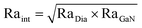 . The general relationship in Fig. 5 is obtained by quadratic fitting and validated by data points with various strain states. The application of tensile strain induces an increase in the surface roughness disparity between the diamond and GaN, thereby reducing the actual contact area at the interface. Moreover, based on the red lines in Fig. S5 (ESI†), the tensile strain alleviates the σx and σy induced by the lattice mismatch. This weakens the interatomic interactions, leading to a reduction in TBC. In contrast, compressive strain mitigates the surface roughness disparity between the diamond and GaN at the interface, thereby increasing the interfacial contact area, and amplifying the σx and σy induced by lattice mismatch, as shown by the blue lines in Fig. S5 (ESI†). This enhances the interatomic interactions at the interface, leading to a substantial increase in TBC.
 |
| | Fig. 5 A general relationship between the TBC and overall interfacial roughness. The general relationship is obtained by quadratic fitting and validated by data points with various strain states. | |
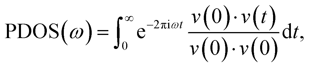
Besides, to elucidate the underlying phonon mechanism, the phonon density of states (PDOS) of the GaN and diamond at the heterostructure interface are investigated. The PDOS was obtained by the Fourier transform of the atomic velocity autocorrelation function (VACF) as follows:
| | 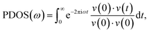 | (2) |
where
ω is the frequency, and
v(
t) is the atomic velocity vector and represents the time average.
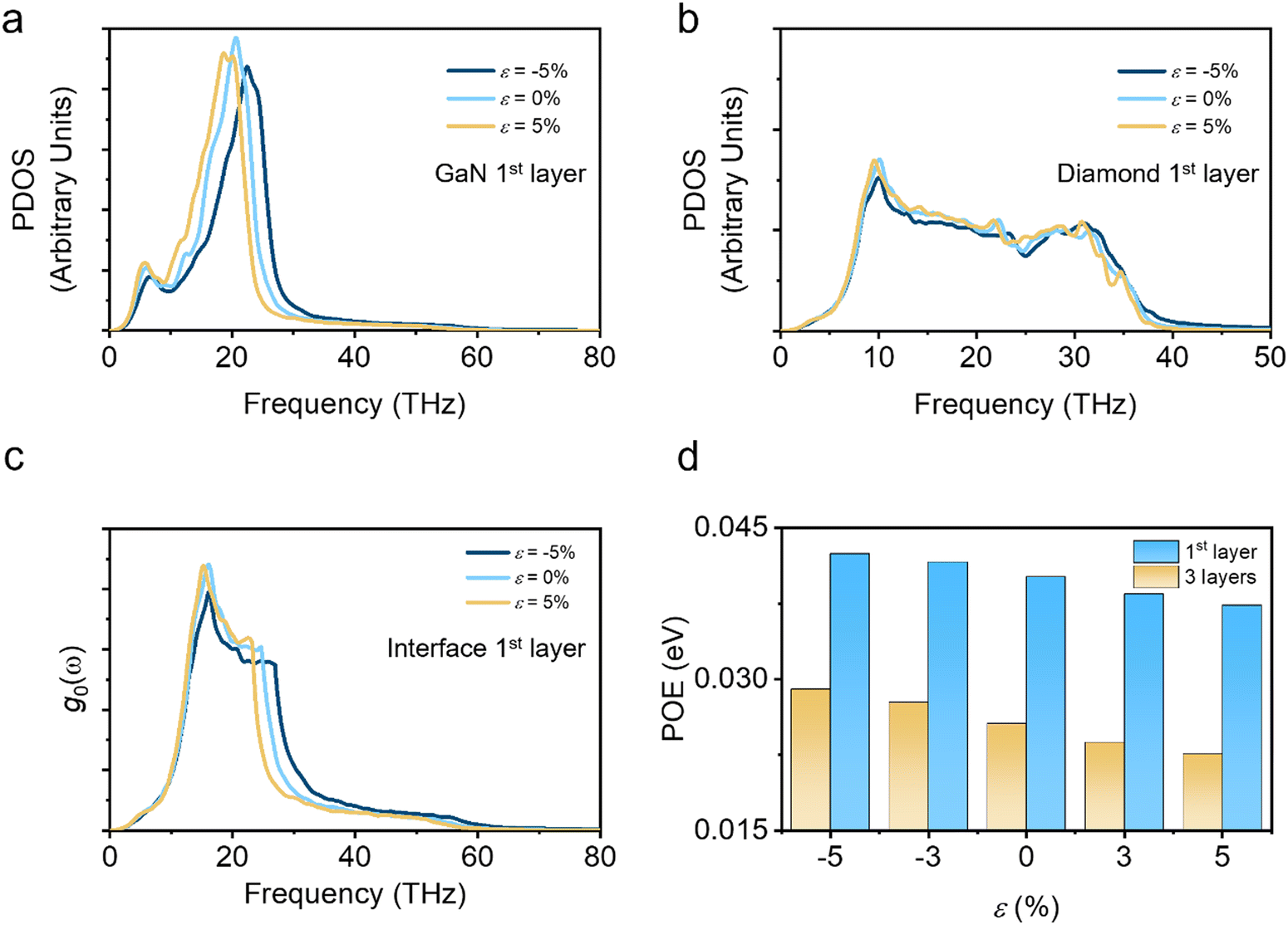
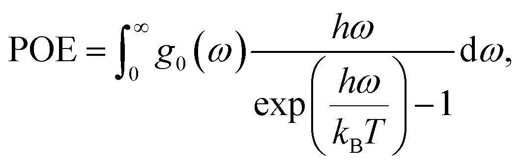
45,46Fig. 6a and b shows the PDOS of the first-layer atoms on the surface of GaN and diamond at the interface, respectively. The PDOS of GaN exhibits a frequency range of up to ∼40 THz, which is characterized by a pronounced phonon peak at 20 THz. Compared to the spectrum at
ε = 0% (light blue curve), both tensile (yellow curve) and compressive (dark blue curve) strains suppress the peak at 20 THz. Moreover, the tensile strain induces a red shift in GaN PDOS, whereas the compressive strain causes a blue shift. In contrast to GaN, the PDOS in diamond is less sensitive to strain. The different phonon responses to strain in GaN and diamond are associated with unequal deformation. Specifically, the effective strain is larger in GaN than in diamond, leading to more significant changes in the phonon spectra. In a similar vein, an analysis was also performed on the PDOS of diamond and GaN in the stress variation region (comprising three layers) at the interface, and the behavior of the corresponding phonon spectra was similar, as shown in Fig. S8 (ESI
†).
 |
| | Fig. 6 Phonon density of states, overlap regions and phonon overlap energy at the GaN/diamond interface under various external mechanical loadings. (a) Phonon density of states of the 1st layer atom on the surface of GaN at the interface. (b) Phonon density of states of the 1st layer atom on the surface of diamond at the interface. (c) The overlap region of phonon density of states between GaN and diamond at the interface. (d) The phonon overlap energy is obtained with one (blue) and three (yellow) layers of atoms closest to the interface. | |
The response of the phonon spectra to mechanical strain alters the overlap region g0(ω) of the PDOS and phonon overlap energy (POE). The overlap region of the PDOS was calculated as follows47: g0(ω) = min{PDOSDia(ω), PDOSGaN(ω)}, where PDOSDia(ω) and PDOSGaN(ω) are the PDOS of diamond and GaN, respectively. Fig. 6c shows the overlap region of the PDOS between the diamond and GaN. The compressive strain extends the overlapping region of the spectra, while the tensile strain reduces the overlap. Moreover, the POE was evaluated to quantify the impact of the variation in g0(ω) on TBC, calculated as follows:
| |  | (3) |
where
h is Planck's constant,

is the Boltzmann distribution,
kB is the Boltzmann constant, and
T is the temperature.
47Fig. 6d presents the POE obtained with one and three layers of atoms closest to the interface and various
ε. As the strain is incrementally increased from −5% to +5%, the POE at the interface exhibits a monotonic decrease. This trend holds for the results obtained with either the atoms at the interface or the atoms throughout the stress variation region (three layers). The greater the phonon overlap energy, the higher the phonon resonance, which corresponds to an enhancement in the TBC.
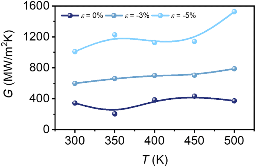
Moreover, the positive impact of compressive strain on TBC at varying temperatures T is also investigated. Fig. 7 shows the relationship between G and T with various magnitudes of compressive strain. For a given T, compressive strain can systematically enhance TBC at different temperatures between 300 and 500 K, and such enhancement is more significant than the variation in G due to temperature.
 |
| | Fig. 7 The relationship between G and T for various magnitudes of compressive strain. | |
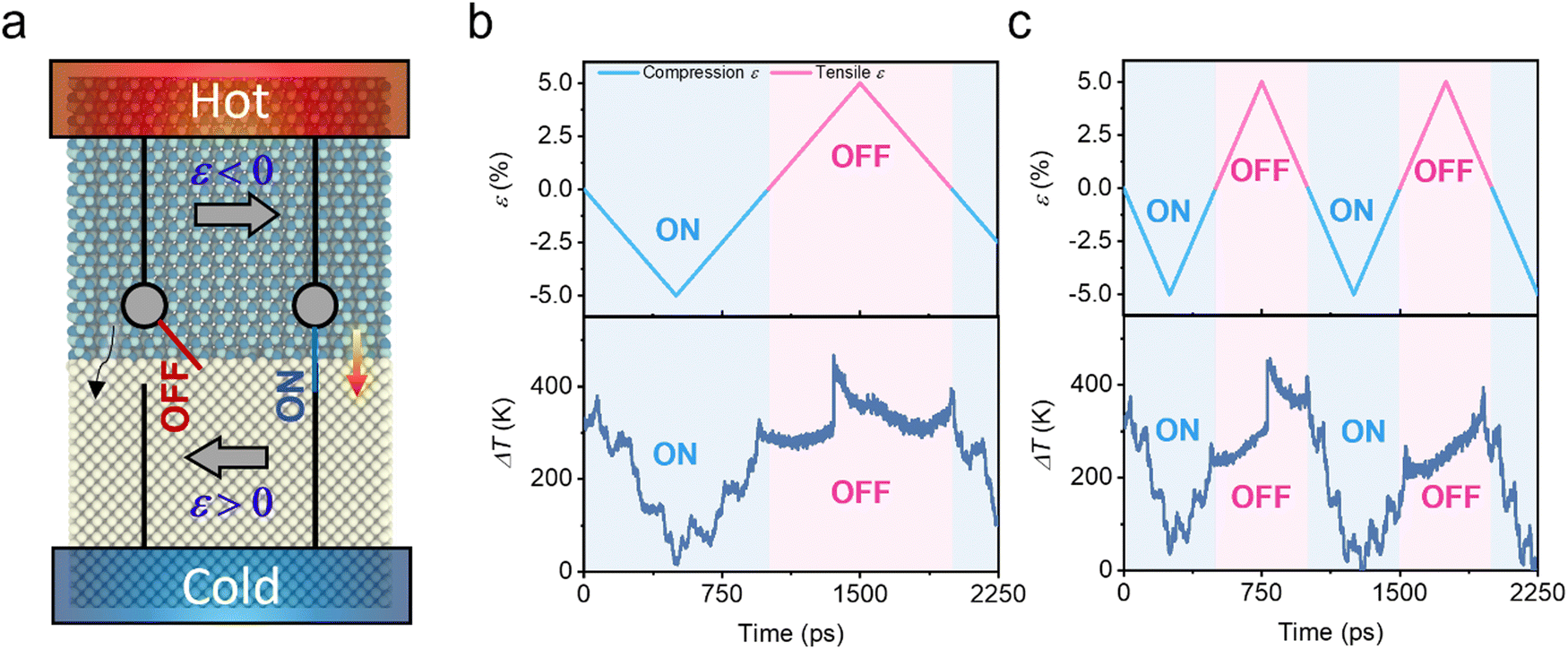
Conceptual design of a mechanical thermal switch
Based on the large tunability in G of almost 400% with respect to mechanical strain, we propose a conceptual design of the “mechanical thermal switch”. Fig. 8a shows a schematic diagram of the mechanical thermal switch and its working principle. A mechanical thermal switch can be utilized to regulate the heat conduction across the interface of GaN and diamond, which serve as the hot and cold ends, respectively. Mechanical loading on the current heterostructure can be achieved by integrating deformable materials in the structural design and applying external mechanical stimulation.39,48 With external tensile strain (ε > 0), the switch is turned “off” (left), which limits the heat conduction across the interface. In contrast, if compressive strain is exerted on the thermal switch, it is turned “on” (right), facilitating heat transfer at the interface. It is worth noting that the “on” and “off” states can be dynamically shifted as long as the magnitude of loading is below the yielding point, and the deformation is reversible. If a constant heat flux is applied across the interface, the thermal switch can adjust the temperature drop ΔT.
 |
| | Fig. 8 A conceptual design of the mechanical thermal switch. (a) Schematic diagram of the mechanical thermal switch and working principle. With an external tensile strain (ε > 0), the switch is turned “off” (left). In contrast, if compressive strain is exerted on the thermal switch, it is turned “on” (right). (b) and (c) The regulation function of the mechanical thermal switch. The upper plot shows the applied mechanical strain, which varies between ±5%, switching the “on” (blue) and “off” (red) states. The temporal durations of the blue and red regions are 1 ns. The corresponding evolution of ΔT is displayed in the lower plot. | |
Fig. 8b shows the regulation function of the mechanical thermal switch, where a constant heat flux J of 50 GW m−2 is imposed across the interface and generates an initial temperature drop of 300 K. The upper plot shows the applied mechanical strain, which varies between ±5%, switching the “on” (blue) and “off” (red) states. The temporal durations of the blue and red regions are 1 ns. The corresponding evolution of ΔT is displayed in the lower plot, where the locations of the major peaks and valleys are highly consistent with the maximum and minimum values of ε. This agreement suggests that the regulation function with continuously varying strain is effective without a notable delay. The mechanical thermal switch can achieve a 400 K variation in the temperature drop between the hot and cold ends. Fig. 8c presents another demonstration with similar settings but a loading rate twice that shown in Fig. 8b. Likewise, ΔT at an elevated loading rate also exhibits a fast response to mechanical loading. This mechanical thermal switch can be used in high-power electronic devices, heat dissipation, thermal storage systems, and thermal management applications.49,50
Conclusions
In summary, we have demonstrated that external mechanical loading can notably alter the thermal boundary conductance of a GaN/diamond heterostructure with a variation range close to ∼400% due to the mechanically tunable interface morphology and phonon resonance. The mechanical tunability of the thermal boundary conductance remains constant at various temperatures. Molecular dynamics simulations reveal that the lattice mismatch between GaN and diamond results in a severe atomic stress at the bonding interface. The stress distribution is characterized by periodic patterns that remain with external mechanical loading. In addition, the lattice mismatch induces stress concentration when subjected to external loading, reducing the mechanical strength at the interface of the heterostructure. Therefore, failure and crushing due to tensile and compressive strain generally occur at the interface. The tensile/compressive strain at the interface enhances/reduces the surface roughness, promotes/suppresses the interaction strength, and hence, increases/decreases the interfacial thermal conductance. A general regulation law can be established between the TBC and the overall surface roughness under various stress states. Besides, mechanical loading leads to unequal deformation of GaN and diamond due to their contrasting elastic moduli. The effective strain in GaN is always higher than that in diamond. The analyses of the phonon spectra indicate that the red/blue shifts of phonon peaks in GaN are more pronounced than those in diamond subjected to external tensile/compressive loading, leading to enhanced/reduced overlapping regions in the phonon spectra. The variation in overlapping regions of the phonon spectra is related to the change in the phonon overlap energy, which alters the phonon transmission across the interface, and the thermal boundary conductance. Based on the correlation between the thermal boundary conductance and external mechanical loading, we proposed a conceptual design of a “mechanical thermal switch”, which effectively regulates the heat flux across the interface with external tensile and compressive loading. For a constant heat flux of 50 GW m−2, the temperature drop at “on” and “off” states can be adjusted by 400 K without a notable temporal delay. This work offers a fundamental understanding of the atomic-level interfacial thermal transport in GaN/diamond heterostructures subjected to mechanical loading. The results and underlying mechanisms are critical for the thermal management of next-generation high-power electronic devices. The interplay between nanoscale thermal transport and mechanics sheds light on the design and development of downsized thermal and energy devices with mechanically tunable performances.
Methods
Atomistic modeling
The atomistic model of the GaN/diamond heterostructure adopted in the MD simulations consists of bulk diamond and GaN, as displayed in Fig. 1a. The dimensions of the heterostructure are 7.5 (in x) × 7.5 (in y) × 30.0 nm (in z), and diamond and GaN possess the same size of 15.0 nm in the z-direction. Diamond and GaN have a diamond cubic lattice structure and a wurtzite crystal structure, respectively, with lattice constants of adiamond = 3.567 Å and aGaN = 3.189 Å. The (001) and (0001) crystallographic planes are selected as the x–y plane of the diamond and GaN layers, respectively, and the c-axes of the diamond and GaN are aligned in the z-direction. Periodic boundary conditions were applied in the x- and y-directions, and a nonperiodic boundary condition was used in the z-direction.
Molecular dynamics simulations
All classic MD simulations were conducted using the open-source platform LAMMPS (large-scale atomic molecular massively parallel simulator).51 A three-body Tersoff potential was utilized to describe the interactions between carbon, gallium, and nitrogen atoms in the system, including the interface of the heterostructures. The Tersoff potential has been widely used to investigate the mechanical and thermal properties of similar hybrid systems.40,52 The time step was 1 fs. The neighbor skin was set to 2.0 with the bin style, and the neighbor list was updated every 500 steps to ensure the accuracy of the thermal calculations. After the initial minimization, the system was relaxed at 300 K with a constant temperature and pressure (NPT) for 500 ps, followed by another 500 ps of relaxation in the canonical (NVT) ensemble. After relaxation, the atoms within 10 Å from both ends were treated as fixed regions.
The tensile/compressive strain was introduced by remapping the z-coordinate of atoms uniformly in every step. The equivalent strain rate was 108 s−1, which is usually adopted to study the quasi-static mechanical behavior of similar systems.53,54 Under such a loading rate, the structure of the system can be rearranged to reflect the unequal deformation in diamond and GaN of the heterostructure. The nominal strain ε was determined as
| |  | (4) |
where Δ
l and
lz are the applied deformation and the original dimensions of the system in the
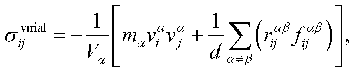
z-direction, respectively. After exerting the displacement loading, the structure was relaxed with the NVT ensembles for 200 ps before calculating the stress and thermal properties. The stress tensor for the atom
α was calculated according to
| | 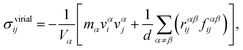 | (5) |
where
α and
β represent atoms,
V is the atomic volume,
m is the atomic mass,
v is the atomic velocity,
r is the inter-atomic distance and
f is the inter-atomic force. The index
d = 2, 3 represents two-body, three-body interactions. The subscripts
i and
j take on values
x,
y, and
z to generate the components of the tensor.
55,56 The values in 200
![[thin space (1/6-em)]](https://www.rsc.org/images/entities/char_2009.gif)
000 steps were used to compute the average stress values to ensure the accurate mapping of stress distributions.
The thermal computation was conducted using a microcanonical (NVE) ensemble. The reverse non-equilibrium molecular dynamics (RNEMD) method was adopted to introduce a constant heat flux in the z-direction by continuously supplying/subtracting the kinetic energy in the hot/cold reservoir.57 The system was divided into 100 slabs in the z-direction, and the three slabs closest to the fixed region at each end were selected as the hot and cold reservoirs. In accordance with GaN-on-diamond high-power devices, where heat accumulation occurs in GaN, the hot and cold reservoirs are set in the GaN and diamond domains, respectively. After a parametric study, the magnitude of the heat flux J was determined to be 50 GW m−2, which typically generates a temperature drop of ∼150 K at the interface of the heterostructure. Such a temperature difference can suppress the uncertainty in thermal calculations and is usually adopted in previous studies.52,58,59 A stable temperature profile can be established after 600 ps, and the temperature results were averaged over 100 ps to reduce the random error against the thermodynamic noise. The thermal boundary conductance TBC (denoted as G) was determined as follows:
| |  | (6) |
where Δ
T is the temperature drop obtained from the temperature profiles within the interface region (see Fig. S1, ESI
†).
60
Author contributions
Y. G. conceived and designed the project. Y. G. and X. Y. planned the computational methods. X. Y and Y. L performed the simulation and analyzed the data. R. C. provided the computational resource. Y. G., B. X. and R. C. supervised the project. X. Y., Y. L., R. C., B. X., and Y. G. wrote the first draft of the manuscript. All authors participated in the discussion and revision of this manuscript.
Data availability
The authors declare that the data supporting the findings of this study are available within the paper.
Conflicts of interest
The authors declare no competing interests.
Acknowledgements
This work was financially supported by the Overseas Outstanding Youth Foundation of the National Natural Science Foundation of China (Grant No. 0214100234). Y. G. acknowledges the support from the Knowledge Innovation Program of Wuhan – Basic Research. R. C. acknowledges the support from the National Key R&D Program of China (Grant No. 2022YFF1500400) and the New Cornerstone Science Foundation through the XPLORER PRIZE.
References
- T. Feng, H. Zhou, Z. Cheng, L. S. Larkin and M. R. Neupane, ACS Appl. Mater. Interfaces, 2023, 15, 29655–29673 CrossRef CAS.
- H. Mashiko, K. Oguri, T. Yamaguchi, A. Suda and H. Gotoh, Nat. Phys., 2016, 12, 741–745 Search PubMed.
- M. Meneghini, C. De Santi, I. Abid, M. Buffolo, M. Cioni, R. A. Khadar, L. Nela, N. Zagni, A. Chini and F. Medjdoub, J. Appl. Phys., 2021, 130, 181101 CrossRef CAS.
- X. Hong, Y. Huang, Q. Tian, S. Zhang, C. Liu, L. Wang, K. Zhang, J. Sun, L. Liao and X. Zou, Adv. Sci., 2022, 9, 2202019 CrossRef CAS.
- L. Nela, N. Perera, C. Erine and E. Matioli, IEEE Trans. Power Electron., 2020, 36, 7412–7416 Search PubMed.
- A. Jafari, M. S. Nikoo, N. Perera, H. K. Yildirim, F. Karakaya, R. Soleimanzadeh and E. Matioli, IEEE Trans. Power Electron., 2020, 35, 12595–12600 Search PubMed.
- N. Ikeda, Y. Niiyama, H. Kambayashi, Y. Sato, T. Nomura, S. Kato and S. Yoshida, Proc. IEEE, 2010, 98, 1151–1161 CAS.
- U. K. Mishra, L. Shen, T. E. Kazior and Y.-F. Wu, Proc. IEEE, 2008, 96, 287–305 CAS.
- L. Gill, S. DasGupta, J. Neely, R. Kaplar and A. Michaels, IEEE Trans. Power Electron., 2024, 39, 517–537 Search PubMed.
- Y. Yin and K. B. Lee, IEEE Electron Device Lett., 2022, 43, 533–536 CAS.
- L. Zhao, C. Liu and K. Wang, Small, 2022, 18, 2106757 CrossRef CAS.
- B. N. Pushpakaran, A. S. Subburaj and S. B. Bayne, J. Electron. Mater., 2020, 49, 6247–6262 CrossRef CAS.
- T. Kim, C. Song, S. I. Park, S. H. Lee, B. J. Lee and J. Cho, Int. Commun. Heat Mass Transfer, 2023, 143, 106682 CrossRef CAS.
- Y. Won, J. Cho, D. Agonafer, M. Asheghi and K. E. Goodson, IEEE Trans. Compon., Packag., Manuf. Technol., 2015, 5, 737–744 CAS.
- J. H. Leach and H. Morkoc, Proc. IEEE, 2010, 98, 1127–1139 CAS.
- Z. Yan, G. Liu, J. M. Khan and A. A. Balandin, Nat. Commun., 2012, 3, 827 CrossRef PubMed.
- J. Millan, P. Godignon, X. Perpiñà, A. Pérez-Tomás and J. Rebollo, IEEE Trans. Power Electron., 2013, 29, 2155–2163 Search PubMed.
- J. P. Kozak, R. Zhang, M. Porter, Q. Song, J. Liu, B. Wang, R. Wang, W. Saito and Y. Zhang, IEEE Trans. Power Electron., 2023, 38, 8442–8471 Search PubMed.
- Q. Zheng, C. Li, A. Rai, J. H. Leach, D. A. Broido and D. G. Cahill, Phys. Rev. Mater., 2019, 3, 014601 CrossRef CAS.
- R. Kagawa, Z. Cheng, K. Kawamura, Y. Ohno, C. Moriyama, Y. Sakaida, S. Ouchi, H. Uratani, K. Inoue, Y. Nagai, N. Shigekawa and J. Liang, Small, 2024, 20, 2305574 CrossRef CAS.
- Y. Zhou, J. Anaya, J. Pomeroy, H. Sun, X. Gu, A. Xie, E. Beam, M. Becker, T. A. Grotjohn, C. Lee and M. Kuball, ACS Appl. Mater. Interfaces, 2017, 9, 34416–34422 CrossRef CAS PubMed.
- J. Isberg, J. Hammersberg, E. Johansson, T. Wikström, D. J. Twitchen, A. J. Whitehead, S. E. Coe and G. A. Scarsbrook, Science, 2002, 297, 1670–1672 CrossRef CAS PubMed.
- R. Soleimanzadeh, M. Naamoun, A. Floriduz, R. A. Khadar, R. van Erp and E. Matioli, ACS Appl. Mater. Interfaces, 2021, 13, 43516–43523 CrossRef CAS PubMed.
- K. Wang, K. Ruan, W. Hu, S. Wu and H. Wang, Scr. Mater., 2020, 174, 87–90 CrossRef CAS.
- D. E. Field, J. A. Cuenca, M. Smith, S. M. Fairclough, F. C. Massabuau, J. W. Pomeroy, O. Williams, R. A. Oliver, I. Thayne and M. Kuball, ACS Appl. Mater. Interfaces, 2020, 12, 54138–54145 CrossRef CAS.
- T. Matsumae, Y. Kurashima, H. Takagi, Y. Shirayanagi, S. Hiza, K. Nishimura and E. Higurashi, Scr. Mater., 2022, 215, 114725 CrossRef CAS.
- M. Malakoutian, D. E. Field, N. J. Hines, S. Pasayat, S. Graham, M. Kuball and S. Chowdhury, ACS Appl. Mater. Interfaces, 2021, 13, 60553–60560 CrossRef CAS.
- T. Matsumae, S. Okita, S. Fukumoto, M. Hayase, Y. Kurashima and H. Takagi, ACS Appl. Nano Mater., 2023, 6, 14076–14082 CrossRef CAS.
- F. Mu, R. He and T. Suga, Scr. Mater., 2018, 150, 148–151 CrossRef CAS.
- J. Liang, A. Kobayashi, Y. Shimizu, Y. Ohno, S. W. Kim, K. Koyama, M. Kasu, Y. Nagai and N. Shigekawa, Adv. Mater., 2021, 33, 2104564 CrossRef CAS.
- B. L. Hancock, M. Nazari, J. Anderson, E. Piner, F. Faili, S. Oh, D. Twitchen, S. Graham and M. Holtz, Appl. Phys. Lett., 2016, 108 Search PubMed.
- F. Mu, B. Xu, X. Wang, R. Gao, S. Huang, K. Wei, K. Takeuchi, X. Chen, H. Yin and D. Wang, J. Alloys Compd., 2022, 905, 164076 CrossRef CAS.
- E. Brusaterra, E. B. Treidel, F. Brunner, M. Wolf, A. Thies, J. Würfl and O. Hilt, IEEE Electron Device Lett., 2023, 44, 388–391 CAS.
- J. W. Pomeroy, M. Bernardoni, D. C. Dumka, D. M. Fanning and M. Kuball, Appl. Phys. Lett., 2014, 104, 083513 CrossRef.
- Y. Gao, Q. Liu and B. Xu, ACS Nano, 2016, 10, 5431–5439 CrossRef CAS.
- Y. Gao and B. Xu, ACS Nano, 2018, 12, 11254–11262 CrossRef CAS PubMed.
- Y. Gao and B. Xu, ACS Appl. Mater. Interfaces, 2017, 9, 34506–34517 CrossRef CAS.
- Y. Gao, W. Yang and B. Xu, Carbon, 2016, 96, 513–521 CrossRef CAS.
- Y. Zhou, Z.-Y. Dong, W.-P. Hsieh, A. F. Goncharov and X.-J. Chen, Nat. Rev. Phys., 2022, 4, 319–335 CrossRef CAS.
- C. Yang, J. Wang, D. Ma, Z. Li, Z. He, L. Liu, Z. Fu and J.-Y. Yang, Int. J. Heat Mass Transfer, 2023, 214, 124433 CrossRef CAS.
- X. Zhao and W. Hu, Surf. Interfaces, 2024, 104178 CrossRef CAS.
- Y. Zhang, H. Sun and C. Chen, Physical Review B: Condens. Matter Mater. Phys., 2006, 73, 144115 CrossRef.
- X. Luo, Z. Liu, B. Xu, D. Yu, Y. Tian, H.-T. Wang and J. He, J. Phys. Chem. C, 2010, 114, 17851–17853 CrossRef CAS.
- Y. Qian, F. Shang, Q. Wan and Y. Yan, AIP Adv., 2017, 7, 095312 CrossRef.
- J. Dickey and A. Paskin, Phys. Rev., 1969, 188, 1407 CrossRef CAS.
-
M. P. Allen and D. J. Tildesley, Computer simulation of liquids, Oxford university press, 2017 Search PubMed.
- V. Panneerselvam, A. Anandakrishnan and S. P. Sathian, Phys. Chem. Chem. Phys., 2023, 25, 6184–6193 RSC.
- B. R. Ram, V. Malik, B. K. Naik and K. S. Patel, Heat Transfer Eng., 2023, 44, 1789–1802 CrossRef CAS.
- Y. Zeng, B. Zhang, Y. Fu, F. Shen, Q. Zheng, D. Chalise, R. Miao, S. Kaur, S. D. Lubner and M. C. Tucker, Nat. Commun., 2023, 14, 3229 CrossRef CAS.
- J. B. Puga, B. D. Bordalo, D. J. Silva, M. M. Dias, J. H. Belo, J. P. Araújo, J. C. Oliveira, A. M. Pereira and J. Ventura, Nano Energy, 2017, 31, 278–285 CrossRef CAS.
- A. P. Thompson, H. M. Aktulga, R. Berger, D. S. Bolintineanu, W. M. Brown, P. S. Crozier, P. J. in’t Veld, A. Kohlmeyer, S. G. Moore and T. D. Nguyen, Comput. Phys. Commun., 2022, 271, 108171 CrossRef CAS.
- L. Tao, S. Theruvakkattil Sreenivasan and R. Shahsavari, ACS Appl. Mater. Interfaces, 2017, 9, 989–998 CrossRef CAS.
- S. C. Chowdhury and J. W. Gillespie Jr, Composites, Part B, 2022, 237, 109877 CrossRef CAS.
- L. Lv, M. Yang, Y. Long and J. Chen, Appl. Surf. Sci., 2021, 557, 149823 CrossRef CAS.
- D. M. Heyes, Physical Review B: Condens. Matter Mater. Phys., 1994, 49, 755 CrossRef CAS.
- A. P. Thompson, S. J. Plimpton and W. Mattson, J. Chem. Phys., 2009, 131, 154107 CrossRef.
- P. Wirnsberger, D. Frenkel and C. Dellago, J. Chem. Phys., 2015, 143, 124104 CrossRef CAS.
- Z. Wang, F. Sun, Z. Liu, L. Zheng, D. Wang and Y. Feng, ACS Appl. Mater. Interfaces, 2023, 15, 16162–16176 CrossRef CAS.
- A. Petkov, A. Mishra, J. W. Pomeroy and M. Kuball, Appl. Phys. Lett., 2023, 122, 031602 CrossRef CAS.
- S. Plimpton, J. Comput. Phys., 1995, 117, 1–19 CrossRef CAS.
|
| This journal is © The Royal Society of Chemistry 2024 |
Click here to see how this site uses Cookies. View our privacy policy here. 
 a,
Yifan
Li
a,
Renjie
He
a,
Yanwei
Wen
a,
Yifan
Li
a,
Renjie
He
a,
Yanwei
Wen

 , where n is the number of atoms at the surface of diamond or GaN at the interface, h is the difference between the z coordinates of the ith atoms at the interface, and hi is the mean value of the z coordinates
  . The atoms in the first layer closest to the interface are employed to calculate Ra; the detailed layering scheme is illustrated in Fig. S7 (ESI†). RaDia and RaGaN represent the surface roughness of the diamond and GaN at the heterostructure interface, respectively. When ε = 0%, RaDia and RaGaN are 0.407 and 0.408 Å, respectively, which are almost identical. Additionally, the peaks in |h| are finer and denser in diamond than in GaN, which can be attributed to the higher elastic modulus of diamond. External tensile/compressive strain enhances/suppresses deformation at the interface, which generally increases/decreases Ra in both GaN and diamond. With a specific value of ε, Ra is systematically lower in diamond than in GaN due to the smaller deformation in diamond.
 . The general relationship in Fig. 5 is obtained by quadratic fitting and validated by data points with various strain states. The application of tensile strain induces an increase in the surface roughness disparity between the diamond and GaN, thereby reducing the actual contact area at the interface. Moreover, based on the red lines in Fig. S5 (ESI†), the tensile strain alleviates the σx and σy induced by the lattice mismatch. This weakens the interatomic interactions, leading to a reduction in TBC. In contrast, compressive strain mitigates the surface roughness disparity between the diamond and GaN at the interface, thereby increasing the interfacial contact area, and amplifying the σx and σy induced by lattice mismatch, as shown by the blue lines in Fig. S5 (ESI†). This enhances the interatomic interactions at the interface, leading to a substantial increase in TBC.
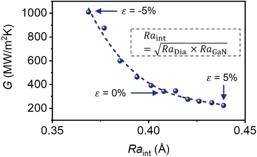
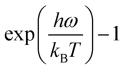 is the Boltzmann distribution, kB is the Boltzmann constant, and T is the temperature.47Fig. 6d presents the POE obtained with one and three layers of atoms closest to the interface and various ε. As the strain is incrementally increased from −5% to +5%, the POE at the interface exhibits a monotonic decrease. This trend holds for the results obtained with either the atoms at the interface or the atoms throughout the stress variation region (three layers). The greater the phonon overlap energy, the higher the phonon resonance, which corresponds to an enhancement in the TBC.