
Two-dimensional layered material photodetectors: what could be the upcoming downstream applications beyond prototype devices?
Yuhang
Ma†
ab,
Huanrong
Liang†
ab,
Xinyi
Guan
 a,
Shuhua
Xu
a,
Meiling
Tao
a,
Xinyue
Liu
*c,
Zhaoqiang
Zheng
*d,
Jiandong
Yao
*ab and
Guowei
Yang
ab
a,
Shuhua
Xu
a,
Meiling
Tao
a,
Xinyue
Liu
*c,
Zhaoqiang
Zheng
*d,
Jiandong
Yao
*ab and
Guowei
Yang
ab
aState Key Laboratory of Optoelectronic Materials and Technologies, Nanotechnology Research Center, School of Materials Science & Engineering, Sun Yat-sen University, Guangzhou 510275, Guangdong, P. R. China. E-mail: yaojd3@mail.sysu.edu.cn
bGuangzhou Key Laboratory of Flexible Electronic Materials and Wearable Devices, Sun Yat-sen University, Guangzhou 510275, Guangdong, P. R. China
cGuangdong Provincial Key Laboratory of Nanophotonic Manipulation, Institute of Nanophotonics, Jinan University, Guangzhou 511443, China. E-mail: liuxinyue8@jnu.edu.cn
dSchool of Materials and Energy, Guangdong University of Technology, Guangzhou 510006, Guangdong, P. R. China. E-mail: zhengzhq5@mail2.sysu.edu.cn
First published on 24th July 2024
Abstract
With distinctive advantages spanning excellent flexibility, rich physical properties, strong electrostatic tunability, dangling-bond-free surface, and ease of integration, 2D layered materials (2DLMs) have demonstrated tremendous potential for photodetection. However, to date, most of the research enthusiasm has been merely focused on developing novel prototype devices. In the past few years, researchers have also been devoted to developing various downstream applications based on 2DLM photodetectors to contribute to promoting them from fundamental research to practical commercialization, and extensive accomplishments have been realized. In spite of the remarkable advancements, these fascinating research findings are relatively scattered. To date, there is still a lack of a systematic and profound summarization regarding this fast-evolving domain. This is not beneficial to researchers, especially researchers just entering this research field, who want to have a quick, timely, and comprehensive inspection of this fascinating domain. To address this issue, in this review, the emerging downstream applications of 2DLM photodetectors in extensive fields, including imaging, health monitoring, target tracking, optoelectronic logic operation, ultraviolet monitoring, optical communications, automatic driving, and acoustic signal detection, have been systematically summarized, with the focus on the underlying working mechanisms. At the end, the ongoing challenges of this rapidly progressing domain are identified, and the potential schemes to address them are envisioned, which aim at navigating the future exploration as well as fully exerting the pivotal roles of 2DLMs towards the practical optoelectronic industry.
 Yuhang Ma | Yuhang Ma obtained his BS degree from Sun Yat-sen University in 2022. He is now studying for his MA degree under the supervision of Prof. Jiandong Yao at the State Key Laboratory of Optoelectronic Materials and Technologies, School of Materials Science & Engineering, Sun Yat-sen University. His current research focuses on pulsed-laser deposition synthesis of low-dimensional materials, design and fabrication of novel photodetectors, and their applications based on optoelectronic properties. |
 Huanrong Liang | Huanrong Liang graduated from Sun Yat-sen University and received his BS degree in materials chemistry in 2023. He continues his graduate study under the supervision of Prof. Jiandong Yao at the School of Material Science & Engineering, Sun Yat-sen University. His research interests include the synthesis of high-quality two-dimensional materials by pulsed-laser deposition, the exploration of their photoelectric properties, as well as the fabrication of high-performance devices and their further applications. |
 Xinyue Liu | Xinyue Liu received her BS degree in Materials Physics from School of Physics Science & Engineering, Sun Yat-sen University in 2015 and her PhD degree in Condensed Matter Physics from School of Physics, Sun Yat-sen University in 2020 under the supervision of Prof. Guowei Yang. Currently, she is an Assistant Professor at the Institute of Nanophotonics, Jinan University. Her research interests include the synthesis of 2D materials and all-dielectric nanomaterials, as well as their applications in nanophotonics and working principles. |
 Zhaoqiang Zheng | Zhaoqiang Zheng received his BS degree in Hunan University (2011) and PhD degree in Sun Yat-sen University (2017). Then, he joined the School of Materials and Energy, Guangdong University of Technology and currently is an Associate Professor. His research interests are the design, synthesis and photodetection applications of novel 2D materials and their heterostructures. |
 Jiandong Yao | Jiandong Yao received his BS degree in Materials Physics in 2013 from School of Physics Science & Engineering, Sun Yat-sen University and his PhD degree in Condensed Matter Physics in 2018 from School of Physics, Sun Yat-sen University under the supervision of Prof. Guowei Yang. Then, he joined the School of Materials Science & Engineering, Nanyang Technological University as a Research Fellow. Currently, he is an Associate Professor in School of Materials Science & Engineering, Sun Yat-sen University. His research interests include the controllable synthesis of low-dimensional materials and their application in optoelectronics. |
1. Introduction
Photodetectors represent functional electronic devices that can convert light signals into electrical signals.1–5 These devices can respond to light irradiation by absorbing incident photons and stimulating electron–hole pairs, thereby generating additional electrical signals that are easily processed in circuits. To date, photodetectors have been exploited in extensive domains, including communications,6,7 imaging,8,9 clinical diagnostics,10 artificial photonic nociceptors,11etc. With the continual progress of science and technology, the application scope of photodetectors is also constantly expanding, bringing more convenience, opportunities, and possibilities to people's lives and work.Traditional optoelectronic devices have mainly relied on bulk covalent semiconductors such as silicon, germanium, gallium arsenide, lead sulfide, mercury cadmium telluride, etc. The constituent atoms of these materials are interconnected through strong covalent bonds along any direction, which makes the preparation and processing of the corresponding photodetectors quite complex and costly. In addition, these bulk materials suffer from high brittleness, making it difficult for them to be competent for wearable forms that need to undergo bending, folding, and stretching. Furthermore, traditional covalent photosensitive materials are easily degraded by environmental factors such as temperature and humidity on account of their interceptive surfaces terminated with a large number of active dangling bonds, resulting in unstable photosensitive performance and easy aging/degradation, especially under low-dimensional conditions (i.e. high surface-to-volume ratio). Meanwhile, the numerous interfacial defect states can lead to high background noise and low photosensitivity for the optoelectronic devices based on these materials, thus requiring complex peripheral circuits/noise reduction systems (such as cooling devices) to improve the detection performance of related devices. In consideration of the above formidable challenges, it is essential to search for alternative materials.
Two-dimensional layered materials (2DLMs) are a new family of low-dimensional phase represented by graphene (Gr) and MoS2. This category of materials is composed of a single monolayer or a few self-passivated monolayers. The interactions between the monolayers are weak van der Waals (vdW) forces, while the interactions between atoms within the same monolayer are usually strong covalent bonds.12–16 Compared to traditional bulk covalent semiconductors, 2DLMs manifest a handful of unique advantages. Firstly, due to the extremely thin thickness, 2DLMs exhibit excellent flexibility and conformability. These characteristics allow them to be flexibly integrated on various surfaces, greatly expanding their potential application scenarios and making them widely applicable in wearable devices. Meanwhile, the low-dimensional properties of 2DLMs warrant excellent electrostatic tunability, providing a substantial degree of freedom for device performance modulation. Secondly, the surface of 2DLMs is free of dangling bonds, which markedly reduces the interfacial defects, contributing to suppressing device noise and improving the transport characteristics of charge carriers, thereby improving the photosensitivity of the devices. Meanwhile, such unique structural characteristics allow the construction of 2DLM based heterojunctions to be unconstrained by the lattice-matching conditions.17–32 Therefore, theoretically, the manipulation of photocarrier dynamics and multifunctional photodetection can be achieved through the stacking and synergy of various atomically thin functional layers. On the whole, 2DLMs possess a variety of unique advantages in the field of photodetection, which can overcome the critical shortcomings of traditional bulk materials and bring unprecedented opportunities for the development and application of the next-generation advanced optoelectronic devices. Taking advantage of their abundant and excellent physical properties, researchers have developed various types of photodetectors based on a host of 2DLMs, including elemental semimetals/semiconductors,33–36 post-transition metal chalcogenides,37–41 transition metal chalcogenides,42–51 multi-elemental 2DLMs,52–70 as well as related van der Waals heterostructures.19–22,27,71–87 Inspiringly, these emerging photodetectors have exhibited highly competitive device performance. For example, in 2016, Huang et al. achieved a remarkably high responsivity of 4.3 × 10⁶ A W−1 based on a photoconductive-type black phosphorus nanosheet photodetector,36 far exceeding those of the recently reported metal–semiconductor–metal (MSM) photodetectors built of conventional covalent semiconductors (e.g., Ge (0.572 A W−1),88 GaN (4.23 A W−1),89 SiC (29 mA W−1),90 GaAs (99.01 A W−1)91). In 2019, Sun et al. demonstrated that a flexible MSM photodetector with monolayer MoS2 serving as the light-sensing channel can be durable for up to 10![[thin space (1/6-em)]](https://www.rsc.org/images/entities/char_2009.gif) 000 bending cycles.51 In contrast, flexible photodetectors based on conventional covalent semiconductors commonly suffer from severe degradation after bending treatments (e.g., a degeneration of 56% in photocurrent over 100 bending cycles for a CdSxSe1−x MSM photodetector).92 In 2022, Zeng et al.93 revealed that the response time of a MoS2/WSe2 heterojunction was down to 4 ps, which was substantially shorter than those of Ge/Si (≈ 850 ps)94 and InP/ZnO (≈ 5.8 ns)95 photodiodes. In another study, Schall et al. demonstrated a >76 gigahertz (GHz) MSM photodetector based on graphene,96 which far exceeds those of state-of-the-art MSM photodetectors built of conventional semiconductors (e.g., Si (7.5 GHz),97 GeSn (1.26 GHz),98 InGaAs (2.03 GHz)99). Similarly, Flöry et al. reported a graphene/MoTe2 heterojunction photodetector with a bandwidth up to 50 GHz,100 which was also superior to many of the previous heterojunction photodetectors such as Si/Ge (40 GHz),101 Ge/GaAs (9.3 GHz),102 and InGaAs/InP (3 GHz).103
000 bending cycles.51 In contrast, flexible photodetectors based on conventional covalent semiconductors commonly suffer from severe degradation after bending treatments (e.g., a degeneration of 56% in photocurrent over 100 bending cycles for a CdSxSe1−x MSM photodetector).92 In 2022, Zeng et al.93 revealed that the response time of a MoS2/WSe2 heterojunction was down to 4 ps, which was substantially shorter than those of Ge/Si (≈ 850 ps)94 and InP/ZnO (≈ 5.8 ns)95 photodiodes. In another study, Schall et al. demonstrated a >76 gigahertz (GHz) MSM photodetector based on graphene,96 which far exceeds those of state-of-the-art MSM photodetectors built of conventional semiconductors (e.g., Si (7.5 GHz),97 GeSn (1.26 GHz),98 InGaAs (2.03 GHz)99). Similarly, Flöry et al. reported a graphene/MoTe2 heterojunction photodetector with a bandwidth up to 50 GHz,100 which was also superior to many of the previous heterojunction photodetectors such as Si/Ge (40 GHz),101 Ge/GaAs (9.3 GHz),102 and InGaAs/InP (3 GHz).103
Taking advantage of the fascinating properties, in recent years, researchers have explored a series of emerging optoelectronic applications by using these 2DLM photodetectors as the core functional components. For example, in 2019, Polat et al. successfully exploited a hybrid PbS quantum dots/graphene photodetector for wearable fitness monitoring spanning heart rate, arterial oxygen saturation, and respiratory rate.104 In 2022, Lu et al. reported on multiplexing optical communications based on an O–WS2/WS2 photodetector by using the polarization state and the light intensity as independent transmission channels.105 Most recently, Gao et al. constructed a transparent ZnO/MoS2 photodetector array and harnessed it for an electronic eye consolidating double-sided imaging capabilities.106 These advancements all demonstrate the enormous advantages of 2DLMs in the next-generation optoelectronic industry.
Despite significant progress, these research works are relatively fragmented. Thus far, in spite of the appearance of numerous reviews/tutorials/perspectives regarding 2DLM photodetectors, these literature reports have been largely focused on the materials, devices, effective spectrum, and performance optimization.107–120 Some researchers have recently paid attention to the downstream applications but only focused on a relatively small domain such as infrared imaging.121 To date, to our knowledge, there is still no systematical review regarding the extensive downstream applications of 2DLM photodetectors. This seriously prevents researchers from having a quick, timely, and comprehensive inspection of this fascinating domain and also prevents the further advancement of 2DLM optoelectronic devices from fundamental research to practical production and commercialization. In response to this, in the current review, the emerging downstream applications of 2DLM photodetectors in extensive fields, including imaging, health monitoring, target tracking, optoelectronic logic operation, ultraviolet monitoring, optical communications, automatic driving, and acoustic signal detection, have been systematically summarized, with the focus on the underlying principles. In the end, the ongoing challenges of this rapidly progressing domain have been summarized, and the potential schemes to address them have been envisioned, which aim at navigating the future exploration as well as fully exerting the pivotal role of 2DLMs towards the practical optoelectronic industry.
2. Photoelectric imaging
Optoelectronic imaging is a powerful technology that capitalizes on optoelectronic systems to obtain image information. Basically, it converts the reflected/transmitted light signals from the target into electrical signals, which are then processed to reproduce the morphology of the target in the form of images. Photoelectric imaging technology is of great significance to the breakthrough and extension of human visual ability in terms of sensitivity, spatial resolution, response rate, effective spectral domain, etc. Thus far, optoelectronic imaging technology has entered both civilian and military fields such as photography, medical diagnosis, security monitoring, aerospace, remote sensing, and national defense.Currently, the traditional optoelectronic materials and devices still face a series of insurmountable challenges in imaging applications, including large device volume, low integration level, large weight, narrow effective bandwidth, slow response speed, and strict operating conditions. In recent years, 2DLMs have emerged as promising candidates to take the place of traditional optoelectronic materials. These competitors have excellent electrical and optoelectronic properties, such as high carrier mobility, tunable bandgap, excellent immunity to the short-channel effects, and outstanding light absorption ability. Most notably, the surface of 2DLMs is free of dangling bonds, making it flexible for integration of 2DLMs with complementary properties to achieve ground-breaking performance beyond individuals. These fascinating characteristics have provided 2DLMs with extremely high application value in next-generation optoelectronic imaging applications.
As an example, in 2023, Yi and collaborators constructed a SnS2/MoS2 van der Waals heterostructure photodetector (Fig. 1(a)) and exploited it for a visible imaging application.27 As shown in Fig. 1(b), on account of the distinct bandgap values (≈1.75 eV for MoS2 and ≈1.96 eV for SnS2), the photoresponse of SnS2 and MoS2 is well complementary, enabling the SnS2/MoS2 heterojunction to realize high-performance photosensitivity across a broad visible spectral range. This is understandable since the photoresponse of the SnS2/MoS2 heterojunction photodetector comes from the contributions of both constituent components. In addition, the SnS2/MoS2 heterojunction photodetector exhibits a good reversible photoresponse to the periodic illumination, simultaneously hosting relatively low dark current, large photocurrent, and high on/off ratio (Fig. 1(c)). Furthermore, the rise/decay time is as short as 1.38/0.6 ms. The comprehensive properties make the SnS2/MoS2 heterojunction photodetector highly amenable to visible imaging application. On this basis, the device has been further used as the light-sensing unit in a single-pixel imaging application. As shown in Fig. 1(d), in principle, the light illuminating onto a target will be partially blocked, and the transmitted portion is detected by the SnS2/MoS2 heterojunction photodetector. As a consequence, the outline of the target can be obtained by the photocurrent distribution information. Fig. 1(e) shows the photocurrent mapping images extracted by the SnS2/MoS2 heterojunction photodetector upon red, green, and blue violet light illuminations. Distinct profiles of “SYSU” with relatively sharp margin have been successfully obtained, demonstrating the excellent imaging capability. Thus far, photodetectors built of various 2DLMs and related heterostructures, such as PbI2,122 CuInP2Se6,123 WS2/GaN,124 (PEA)2PbI4/SnP2S6,55 1T′-MoTe2/GaN,125 PbI2/InGaO,126 and In2O3/PbI2,127 have been developed for ultraviolet to visible imaging application, attesting to the prodigious potency of 2DLMs in the imaging field.
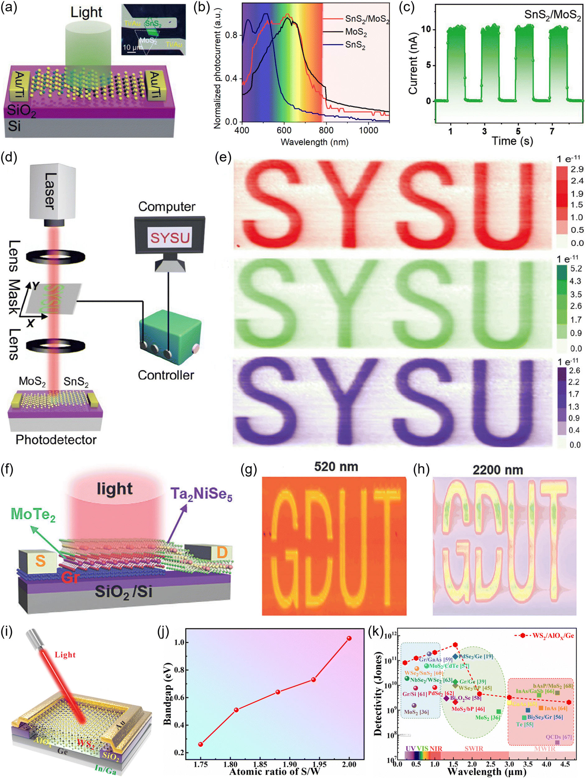 | ||
| Fig. 1 (a) Schematic diagram of a SnS2/MoS2 heterojunction photodetector. The inset presents an optical microscopy image. (b) Spectral photoresponse of the SnS2, MoS2, and SnS2/MoS2 heterojunction photodetectors. (c) Photoswitching curve upon periodic 520 nm illumination. (d) Schematic illustration of the experimental configuration for the single-pixel photoelectric imaging. (e) The imaging profiles for an “SYSU” pattern by using 671 (red), 532 (green), and 405 nm (blue-violet) light as the light source. Reproduced from ref. 27 with permission from Science China Press, copyright 2023. (f) Schematic diagram of a Ta2NiSe5/MoTe2/graphene heterojunction photodetector. (g) and (h) The imaging profiles of a “GDUT” pattern by using 520 (green) and 2200 nm (infrared) light as the light source. Reproduced from ref. 128 with permission from John Wiley and Sons, Inc., copyright 2024. (i) Schematic diagram of a WS2−x/AlOx/Ge heterojunction photodetector. (j) Bandgap value as a function of the S/W ratio of WS2−x. (k) A summary of the detectivity values of the WS2−x/AlOx/Ge heterojunction photodetector under various wavelengths. The detectivity values of other reported 2DLM based devices have also been provided for comparison. Reproduced from ref. 129 with permission from American Chemical Society, copyright 2021. | ||
Despite encouraging research advances, the afore-mentioned studies still face a key challenge of relatively narrow effective spectral range. Compared to ultraviolet and visible light, infrared light has a more excellent penetration ability due to the long wavelength, and it is thus less susceptible to the environmental interference such as haze and smoke. Therefore, in theory, infrared optoelectronic imaging technology possesses a strong anti-interference ability and can be potentially applied in harsh working environments. In addition, due to the benefit of infrared optoelectronic imaging technology being able to utilize the infrared radiation emitted by the targets themselves (any object above 0 K will emit infrared light) for imaging, it theoretically does not rely on external light sources and can thus work normally at night or under weak-light conditions, with excellent night vision ability. On the basis of the above background, exploring new infrared imaging systems based on 2DLMs is an attractive research topic.
As an example, most recently, Zhang et al. have constructed a Ta2NiSe5/MoTe2/Gr van der Waals heterostructure photodetector (Fig. 1(f)) and harnessed this device for ultra-broadband photoelectric imaging application.128 In this device, the top small-bandgap Ta2NiSe5 layer and the middle moderate-bandgap MoTe2 layer serve as light-absorbing layers and form a heterojunction with a built-in electric field facilitating spatial separation of photocarriers, while the bottom graphene layer enables high-efficiency carrier collection. Benefiting from the relatively small bandgap value of Ta2NiSe5, the Ta2NiSe5/MoTe2/Gr device demonstrates a broadband photoresponse across 520 to 2200 nm. Specifically, upon 2200 nm illumination under room temperature, the device realizes a high responsivity of 5.79 A W−1 and an excellent detectivity of 1010 Jones. By exploiting the Ta2NiSe5/MoTe2/graphene heterostructure photodetector as the sensing pixel, visible to near-infrared photoelectric imaging has been demonstrated by accurately reproducing the “GDUT” pattern with clear and distinct boundaries separating the pattern from the background (Fig. 1(g) and (h)). Of note, the effective spectral range of the heterostructured device far exceeds those of human vision (≈ 400–760 nm) and commercial Si-based devices (<1100 nm), thereby manifesting intriguing prospects for future visual systems. Similarly, Zeng et al. fabricated PtTe2/Si heterojunction photodetectors and demonstrated room-temperature visible to far-infrared imaging.130 On the whole, these studies depict a flexible way to achieve infrared imaging by integrating 2DLMs with small bandgap values or gapless band structures. To date, infrared imaging has been realized based on a wealth of 2DLM based photodetectors, including graphene,131 black phosphorus,132 black phosphorus/MoS2,133 PdSe2/Si,134 graphene/PdSe2/Ge,135 PtSe2/Bi2Te3/Si,136etc.
Defect engineering is an effective means of regulating the band structure of low-dimensional materials by tailoring their defects. Therefore, apart from integrating small-bandgap 2DLMs, defect engineering is also one of the potential approaches to realize broadband optoelectronic imaging. In 2021, Wu et al. constructed an ultra-broadband photodetector built of S-deficient WS2 (WS2−x), an AlOx interfacial passivation layer, and Ge (Fig. 1(i)).129 As shown in Fig. 1(j), the bandgap value of WS2 decreases monotonously with increasing sulfur vacancies. Specifically, the estimated bandgap of WS2−x reaches 0.51/0.26 eV for an x value of 0.19/0.25, corresponding to the absorption edge of 2437/4781 nm. On account of the narrow bandgap of WS2−x induced by the vacancy defects, the WS2−x/AlOx/Ge device demonstrates a room-temperature ultra-wide spectral photoresponse spanning from deep ultraviolet (200 nm) to mid-wave infrared (MWIR, 4.6 µm) (Fig. 1(k)). As a consequence, by using the WS2−x/AlOx/Ge heterojunction photodetector as the light-sensing unit, mid-infrared imaging for the “LIGHT” pattern at 4.6 µm has been realized. As a demonstration of the practical application value of infrared imaging, Yu et al. have recently exploited S-deficient ZrS3 infrared photodetectors for imaging a heating tube behind a silicon wafer.48 It was determined that the invisible heating tube can be precisely identified by the eye using the S-deficient ZrS3 infrared photodetector, demonstrating the great potential for non-invasive inspection.
Terahertz waves represent electromagnetic radiation that lies between microwave and infrared light, with unique physical characteristics, making terahertz detection have significant advantages in a variety of fields. For example, the high-resolution characteristics of terahertz waves enable a terahertz radar to detect smaller targets or provide more accurate positioning compared to traditional low-frequency radar. In addition, compared to ultraviolet, visible, and infrared light, terahertz waves have stronger penetration capabilities and can thus efficiently, conveniently, and non-destructively detect hidden explosives, weapons, and other prohibited items. Therefore, terahertz detection has become an important research field. 2D topological semimetals, including Weyl and Dirac semimetals, have raised broad research enthusiasm on account of their special energy band structure containing a Weyl/Dirac cone, which provides these materials with an unlimited light absorption range. As a consequence, these building blocks exhibit great potency in the field of terahertz detection and imaging.
As an example, in 2020, Guo et al. successfully demonstrated a terahertz photodetector based on the type II topological semimetal PdTe2 (0.04–0.3 THz) and successfully harnessed this device for imaging application.137 As shown in Fig. 2(a), the device is composed of a PdTe2 flake as well as symmetrically distributed drain and source electrodes. It exhibits a stable and rapid photoresponse in the frequency range of 0.04–0.3 THz (Fig. 2(b)), showing the tremendous potential for broadband detection. This benefits from the gapless band structure (inset of Fig. 2(a)). As shown in Fig. 2(c), the photoresponse increases linearly with increasing bias voltage. This is because the bias voltage can break the symmetrical plane, making the nonequilibrium carriers move laterally along the electric field. Benefiting from the fast and stable photoresponse, the PdTe2 device is further developed for terahertz imaging application. Fig. 2(d) presents the imaging result for a fresh leaf. The distribution of veins can be clearly identified, which is reasonable as water exhibits strong absorption of terahertz waves. Similarly, the profile of a key can also be well extracted by terahertz imaging (Fig. 2(e)), as metal manifests a strong shielding effect for terahertz waves.
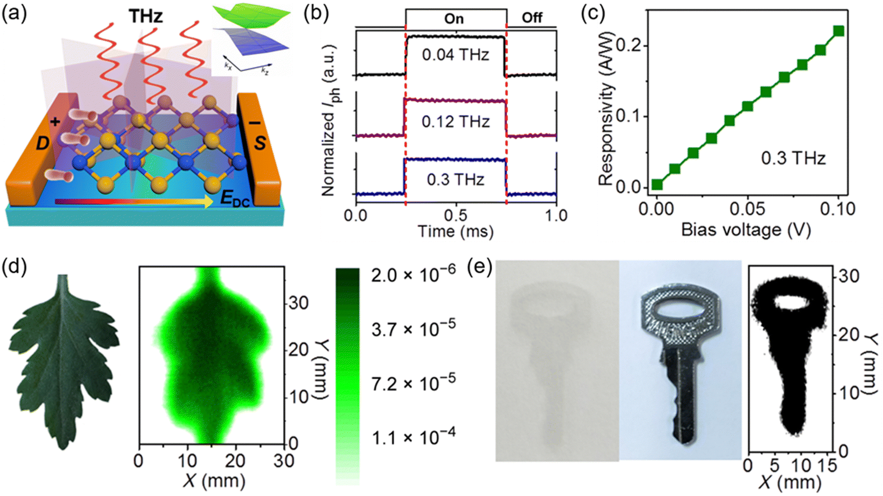 | ||
| Fig. 2 (a) Schematic illustration of the device structure of the PdTe2 photodetector in the biased mode. The inset shows the projection of the Dirac cone along the kx–kz plane. (b) Typical photoswitching curves of the PdTe2-based device under illumination with different photon frequencies. (c) Responsivity as a function of bias voltage upon 0.3 THz illumination. (d) and (e) Results of terahertz imaging for a fresh leaf (0.12 THz) and a hidden key (0.3 THz) by using the PdTe2 photodetector as the sensing pixel. Reproduced from ref. 137 with permission from American Association for the Advancement of Science, copyright 2020. | ||
Thus far, in addition to PdTe2, a series of topological 2D van der Waals materials and related heterostructures, including graphene,138 Bi2Se3,139 Bi2Te2.2Se0.8,140 PtTe2,141 MnBi2Te4,142 NbIrTe4,143 1T-CoTe2,144 ZrGeSe,145 MnBi2Te4/graphene,146 NiTe2/graphene,147 and NbIrTe4/graphene,148 have been harnessed for terahertz sensing. However, in the current stage, there are still some critical issues to be addressed. Firstly, the photosensitivity of the state-of-the-art 2D topological material based terahertz photodetectors still needs to be further improved. In previous studies, due to the relatively high electrical conductivity of semimetallic materials, these devices typically suffer from severe background noise, thereby requiring lock-in amplifiers or low operating temperatures to assist in reading out the photocurrent signals. This will significantly increase the volume, complexity, weight, and cost of the optoelectronic systems, while reducing their portability and integratability in practical applications. Secondly, the vast majority of 2D topological material based terahertz optoelectronic devices have been produced based on cumbersome mechanical exfoliation and stacking techniques.138,139,141 Nevertheless, the device yield of these preparation techniques is quite low. In addition, the lateral size of the exfoliated 2DLMs is substantially limited (≈ tens of micrometers), which curtails their further application in integrated chips demanding arrayed devices. Therefore, it is challenging for these building blocks to meet the needs of practical applications. Finally, many previously studied 2D topological materials, such as PdTe2, PtTe2, TaIrTe4, NbIrTe4, etc., suffer from issues such as complex crystal structures, environmentally unfriendly compositions, low crust reserves, or high material costs, which are not conducive to large-scale commercial applications.
Despite significant research progress, most of the preceding optoelectronic imaging applications have been based on single-pixel modes, which is highly inefficient as the signals have to be extracted in a step-by-step way. As for practical applications, it is often necessary to construct device arrays with small device-to-device variation to significantly improve the efficiency of optoelectronic imaging. As a rule, the key difficulty in preparing device arrays is to achieve scalable preparation of high-quality 2DLMs.
In response to the above predicament, in 2020, Zeng et al. developed a simple two-step growth process to achieve large-scale preparation of 2DLMs.130 As shown in Fig. 3(a), a large-area Pt nanofilm is firstly deposited on the substrate using a magnetron sputtering method. Then, by tellurizing the Pt nanofilm at a relatively high temperature, a large-area PtTe2 nanofilm can thus be obtained. Inspiringly, this technique allows the direct synthesis of a 2D PtTe2 layer on a 2-inch substrate. As shown in Fig. 3(b), PtTe2 nanofilms with different thicknesses can be flexibly prepared by controlling the thickness of the original Pt nanofilms. By combining photolithography technology, arrayed Si windows can be produced by selectively etching away the oxide layer of the SiO2/Si substrate, and PtTe2 nanofilm is subsequently deposited on them to prepare a 4 × 4 PtTe2/Si heterojunction photodetector array and graphene layer is transferred atop to serve as the charge collecting electrode (Fig. 3(c) and (d)). The PtTe2/Si devices exhibit an ultrabroadband photoresponse from ultraviolet to far-infrared (Fig. 3(e)), benefiting from the ultra-wide light absorption of PtTe2 enabled by the gapless band structure (Fig. 3(f)). On this basis, the PtTe2/Si heterojunction photodetector array has been successfully used as the sensing pixels to achieve ultrabroadband multi-pixel optoelectronic imaging applications (Fig. 3(g)). On the whole, this study provides a convenient route to prepare large-area continuous 2DLM nanofilms. In 2023, by tellurizing a pre-deposited Mo nanofilm, Wu et al. achieved the wafer-scale preparation of 1T′-MoTe2 nanofilm.149 Similarly, an 8 × 8 1T′-MoTe2/Si heterojunction photodetector array has been fabricated and multi-pixel imaging for a “heart” pattern has been realized. In another study, by depositing a Pt nanofilm and performing post-selenization treatment, Ye et al. achieved the preparation of centimeter-scale PtSe2 nanofilms.150 On this basis, a 9 × 9 PtSe2/Si heterojunction photodetector array has been constructed and multi-pixel imaging for the “Z”, “J”, and “U” patterns has been realized.
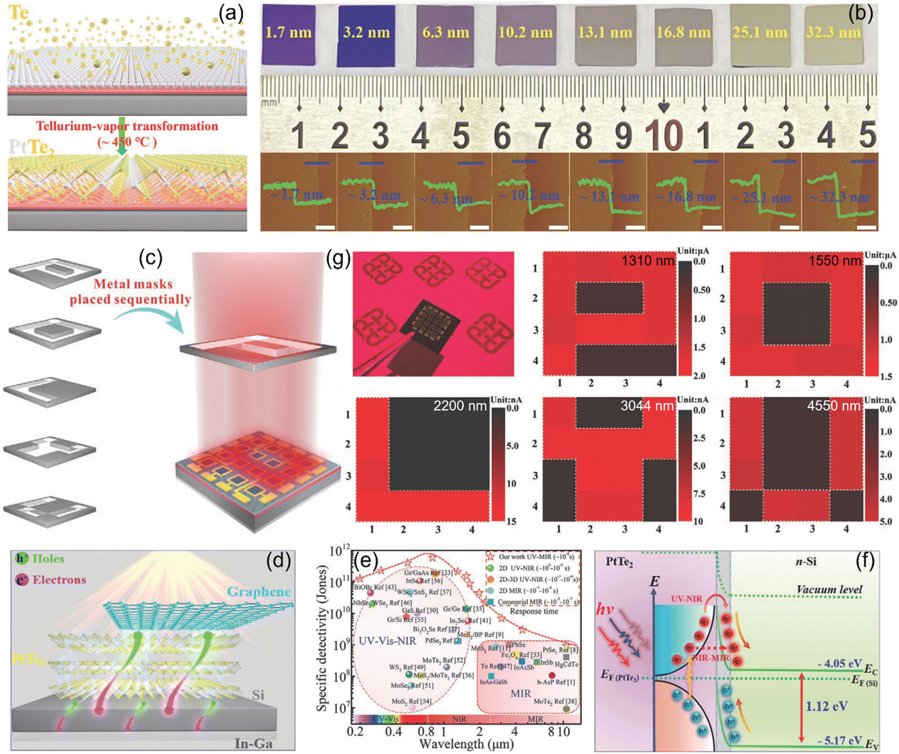 | ||
| Fig. 3 (a) Schematic illustration of the preparation process for producing large-scale PtTe2. (b) Digital photographs and AFM thickness profiles of the PtTe2 nanofilms of different thicknesses. (c) Schematic illustration of the optoelectronic imaging based on an array of PtTe2/Si heterojunction photodetectors. (d) Schematic diagram of the device structure. (e) Spectral photoresponse. (f) Energy band diagram illustrating the working mechanism. (g) Photocurrent mapping images upon 1310 (“P”), 1550 (“O”), 2200 (“L”), 3044 (“Y”), and 4550 (“U”) nm illuminations, respectively. Reproduced from ref. 130 with permission from John Wiley and Sons, Inc., copyright 2020. | ||
To date, in addition to the two-step growth method mentioned above, researchers have also developed other techniques, such as molecular beam epitaxy (MBE),151,152 pulsed-laser deposition (PLD),153,154 and metal–organic chemical vapor deposition (MOCVD),155 to achieve large-scale growth of continuous 2DLMs. These techniques lay a solid foundation for the implementation of multi-pixel optoelectronic imaging application. In the upcoming future, more advancements on multi-pixel optoelectronic imaging can be expected.
Despite the remarkable research progress, most of the 2DLM based optoelectronic imaging research has been based on rigid optoelectronic devices, which greatly limits their practical application scopes. Compared to rigid devices, flexible optoelectronic imaging devices have a series of outstanding advantages. Firstly, flexible optoelectronic imaging devices have excellent bending, twisting and folding capabilities, which enable them to adapt to various complex surfaces. In contrast, it is cumbersome for the rigid optoelectronic imaging devices to adapt to diverse application environments due to their fixed shape. Secondly, flexible optoelectronic imaging devices are usually lighter and thinner than the rigid ones, which makes them more portable. As a result, these devices have extremely high application value in fields requiring strict weight control, such as aerospace and wearable devices. Furthermore, upon external shocks, flexible optoelectronic imaging devices can better buffer external forces through deformation, thus exhibiting better shock resistance. Most importantly, flexible optoelectronic imaging devices can better match different illumination conditions and imaging targets through deformation, providing an additional modulation degree for improving the imaging quality. However, thus far, the research regarding the optoelectronic imaging system of flexible 2DLM photodetectors is still rather limited, predominantly due to the lack of low-temperature synthesis technology for preparing 2DLMs, whereas most flexible substrates are not resistant to high temperature. As such, most flexible 2DLM photodetectors have been fabricated based on manual transfer techniques,156–159 which is impractical for actual applications.
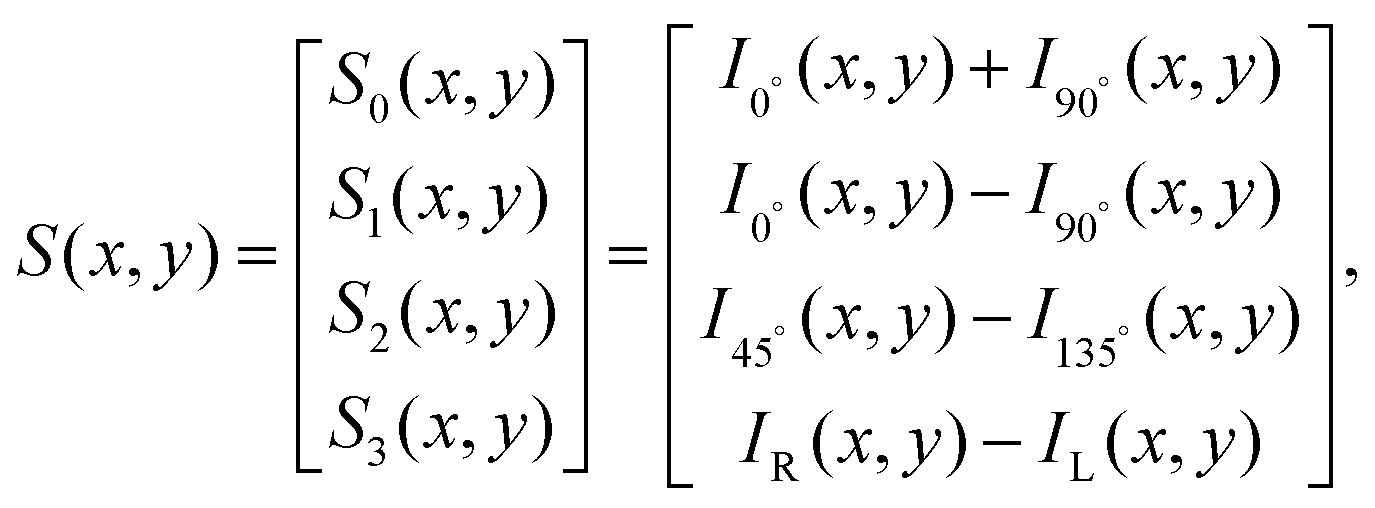
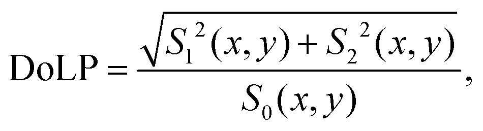
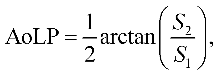
To address this issue, in 2023, Gao et al. developed a spray coating technique for the construction of flexible hybrid MoS2/ZnO photodetectors and successfully exploited them for electronic eyes.106 Specifically, the MoS2 nanosheets are produced using an intercalation-based ultrasonic exfoliation technique. Then, they are composited with ZnO nanoparticles and used for spray coating on flexible transparent poly(vinylalcohol) substrates with prepatterned Ag electrodes (Fig. 4(a)). As shown in Fig. 4(b), the MoS2/ZnO device is well reproducible and has a fast photoresponse. The rise/decay time is as short as 100/250 ms, which can meet the high-speed data acquisition requirements. Therefore, the devices have been further harnessed for e-eye application (Fig. 4(c)). Compared to conventional rigid imagers, the bendable imager can adapt its photosensing area into a curved surface to match the field curvature (Fig. 4(d)). As a consequence, the photocurrent of each imaging pixel can be optimized for image reconstruction, and the imaging for the “E” (Fig. 4(e)) and cross shape (Fig. 4(f)) patterns have been realized. Moreover, with the advantage of the high transparency, imaging from the back side illumination has been demonstrated (Fig. 4(g)), functioning as the insect compound eyes.
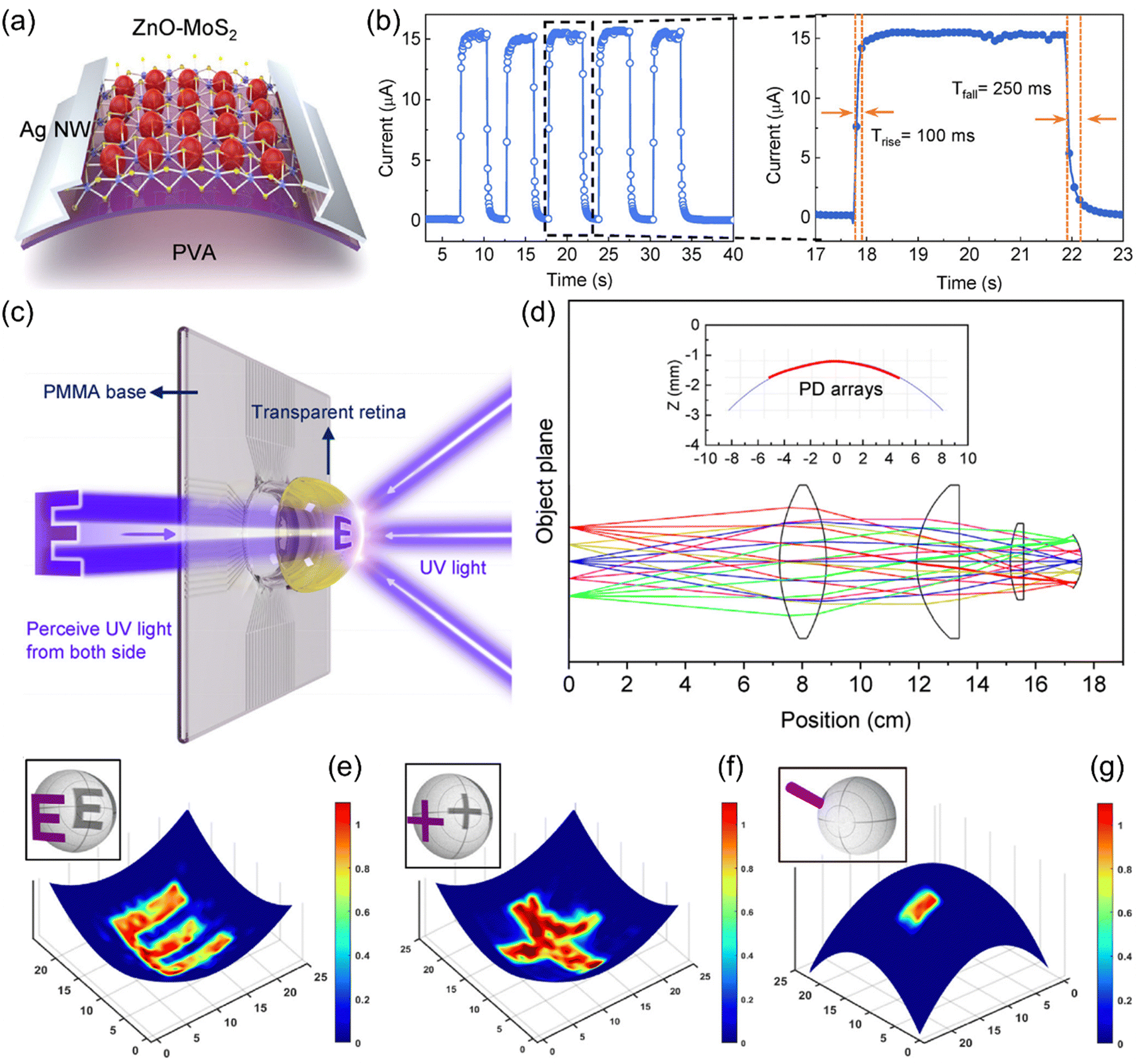 | ||
| Fig. 4 (a) Schematic diagram of a flexible MoS2/ZnO photodetector. (b) Photoswitching curve (left) and an enlarged photoswitching cycle (right). (c) Schematic illustration of an e-eye system based on the flexible MoS2/ZnO photodetectors. (d) Ray-tracing simulation of the lens set-up. Inset: The matched curvature of the photodetector array with the focal plane. (e) and (f) Reconstructed images of the letter “E” and cross shape based on an electronic eye with forward illumination. (g) Reconstructed image of one point based on an electronic eye with backward illumination. Reproduced from ref. 106 with permission from Elsevier, copyright 2023. | ||
In sum, this study provides a unique pathway for the economical and high-efficiency preparation of 2DLM based flexible optoelectronic imaging systems. However, in the current stage, it still suffers from some critical issues. On one hand, although the liquid phase exfoliation technology can be performed at room temperature, the produced photosensitive materials usually suffer from high defect density and interfacial contamination, which seriously plagues the further improvement of device properties. On the other hand, the thin films deposited by spray coating technology are commonly relatively loose, and the long-range stability of the corresponding devices still needs further improvement.
On consideration of these tangible challenges, in recent years, researchers have been devoted to exploring the potential technologies for low-temperature in situ synthesis of 2DLMs directly on flexible substrates.160–164 As an example, in 2017, Zheng et al. demonstrated the direct synthesis of the Mo0.5W0.5Se2 nanofilms on polyimide (PI) substrates by using PLD.161 The low-temperate synthesis probably benefits from the energetic species enabled by the high-energy focused pulsed laser beam. Importantly, the PLD-derived photodetector exhibits a largely unchanged photoresponse over 100 bending cycles. In addition, the growth conditions also play a critical role in the deposition temperature. For example, in 2017, Gong et al. achieved the low-temperature synthesis of MoS2 by optimizing the reaction precursors.162 In this study, (NH4)2MoO4 is used as the Mo source and the deposition temperature is lowered to 450 °C. The mechanism for low-temperature synthesis can be well explained as follows. In the thermodynamic viewpoint, the decomposition of (NH4)2MoO4 to MoO3, H2O, and NH3 can lower the system's overall energy. From the dynamic viewpoint, the MoO3 species from the decomposed (NH4)2MoO4 is more energetic than the MoO3 powder. In addition, the gas produced during the decomposition process can bring the MoO3 molecule out to enable more efficient reaction. As a consequence, the reaction is thermodynamically and kinetically favored. In 2023, Zhang et al. achieved the synthesis of PtSe2 under merely 200 °C by using a plasma-assisted selenization process.164 In principle, the bombardment of Ar plasma can efficiently ionize Se atoms to produce active Se radicals with high chemical reactivity, which is conducive to transforming the Pt nanofilm into the PtSe2 nanofilm. In summary, the above technologies provide highly promising means for the future preparation of high sensitivity flexible optoelectronic imaging systems.
While conventional imaging techniques are highly effective in many situations, in certain specific applications, polarization imaging offers more valuable information and solutions, thus it has been the subject of intensive research. By merging the spatial, spectral, and polarization information of targets, polarization imaging technology not only increases the amount of information obtained from the targets but also enhances the detection capability. With the expanding application scope of polarization imaging in fields such as agriculture, medicine, engineering, atmospheric science, and astronomy, it certainly exhibits broad application prospects in the future. With the requirements for miniaturization and flexibility, 2DLMs offer an important avenue. These materials demonstrate outstanding inherent advantages in being easily integrated into micro/nano optoelectronic devices/systems. Moreover, the high in-plane anisotropy of the crystal structures of a wealth of 2DLMs, including black phosphorus,165 violet phosphorus,166 AsP,167 SiP,168 ReS2,169 ReSe2,170 and PdPSe,171 results in intrinsically anisotropic optical properties. As a consequence, the necessity for integrated optical components has been exempted by constructing polarized photodetectors built of these 2DLMs, reducing simultaneously the processing complexity, volume, and cost.
In 2023, Kong et al. demonstrated contrast-enhanced polarization imaging under scattering illumination based on a 1T′ MoTe2/MoS2 van der Waals heterojunction photodetector (Fig. 5(a)).172 As shown in Fig. 5(b) and (c), the crystal structure of 1T′ MoTe2 exhibits strong in-plane anisotropy. As a consequence, the MoTe2/MoS2 heterojunction device demonstrates pronounced polarization-discriminating photosensitivity. Specifically, the anisotropic ratios are calculated to be 1.77, 1.98, 1.83, and 2.07 upon 852, 915, 1300, and 1550 nm illuminations, respectively. In this study, the MoTe2/MoS2 photodetector is used as a single-pixel imaging sensor and the scattering medium consists of a water solution with 5% volume of milk (Fig. 5(d)). To improve the contrast of imaging results in a scattering environment, traditional light intensity parameters are replaced by a polarization parameter. In theory, the polarization state of an electromagnetic wave can be described using the Stokes vector. The Stokes vector is a 4D vector and can be defined as:
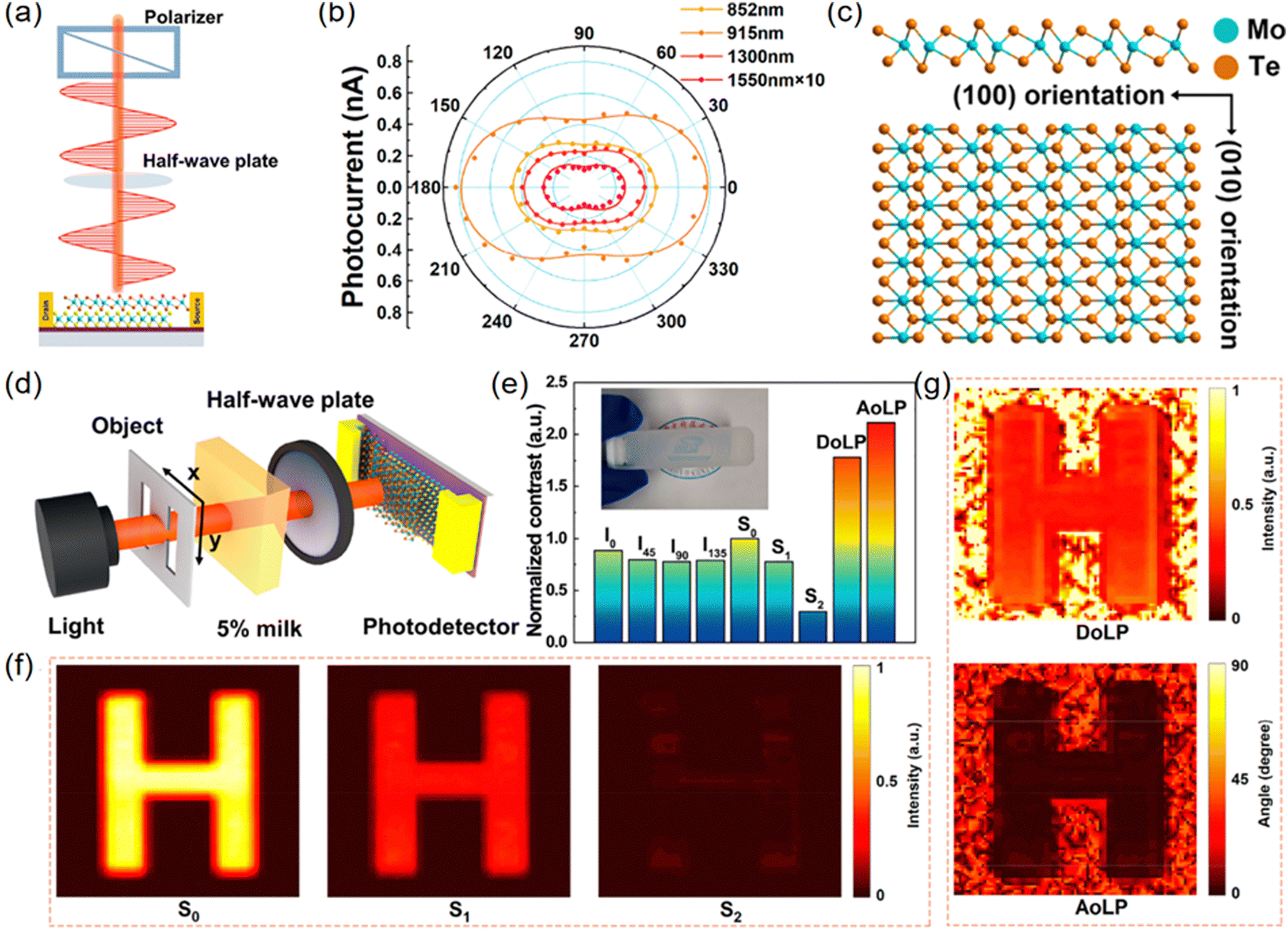 | ||
| Fig. 5 (a) Schematic diagram of polarization detection based on a MoTe2/MoS2 photodetector. (b) Polar plots depicting the photocurrent as a function of polarization angle under 852, 915, 1300, and 1550 nm illuminations. (c) Schematic diagrams of the side view (top) and top view (bottom) of 1T′ phase MoTe2. (d) Schematic of the polarization imaging system in a scattering environment. (e) A summary of the normalized imaging contrast values of various parameters. (f) The imaging results of S0, S1, and S2 under 915 nm light illumination. (g) The imaging results of DoLP and AoLP. Reproduced from ref. 172 with permission from American Chemical Society, copyright 2023. | ||
As shown in Fig. 5(e), the contrast ratio of the output images under various parameters is calculated using the 8-neighbors contrast calculation method and the corresponding imaging results are depicted in Fig. 5(f) and (g). Significantly, the contrast ratios of DoLP and AoLP are 78% and 112% higher than S0, demonstrating that the device has potential for enhanced-contrast polarization imaging. Overall, this study depicts an avenue for increasing the imaging quality based on anisotropic 2DLMs.
In the end, it is to be emphasized that the response rate of photodetectors is one of the key ingredients dominating the imaging efficiency. In the above research work by Kong et al.,172 the response/recovery time of the MoTe2/MoS2 heterojunction photodetectors exceeds 100 µs, which is adverse to the rapid image acquisition. This is probably originated from the unreasonable device design. In a lateral 2DLM heterostructure, the photocarriers need to drift a long distance prior to being collected by the electrodes after these additional charges are separated by the built-in electric field. Fortunately, vertically constructed heterostructures exhibit great potency to overcome this issue.173,174 For example, by using graphene as the top and bottom electrodes, Yan et al. prepared a vertical Gr/GaSe/InSe/Gr heterojunction photodetector.173 Profiting from the shortened transport path and the efficient collection of photocarriers by high-mobility graphene electrodes, the response/recovery time of the device is as short as 1.85/2.05 µs.
3. Health monitoring
Photoplethysmography (PPG), a newly emerged technique relying on photodetection, has been widely used as a non-invasive physiological signal perception technology in the wearable health monitoring field. In principle, PPG utilizes the light scattering/absorption characteristics of tissues and blood for identification of physiological signals. When the heart contracts, the amount of blood in the vessels increases, causing a change in the degree of light reflectance/absorption, finally resulting in a pulsating signal. By processing and analyzing this signal, many useful physiological parameters such as heart rate (HR), blood oxygen saturation (SpO2), and respiratory rate (RR) can be extracted. When using PPG technology for physiological signal identification, photodetectors are usually placed on the skin surface to extract parameters like HR and RR. Under this working condition, the flexibility of the materials/devices is essential. If rigid materials are used, the contact between the sensor and the skin surface may be inadequate, which will lead to a decrease in signal quality. Additionally, rigid materials may make the devices less comfortable to wear and could potentially degrade their durability and reliability. Therefore, it is imperative to consider the use of flexible building blocks to achieve intimate contact quality and comfort level. In this consideration, on account of the atomic-level thickness, 2DLMs exhibit excellent mechanical properties, which enable them to be highly flexible while also possessing favorable optical and electrical characteristics.164,175–177 As a result, these building blocks possess tremendous potential for advancing the field of wearable health monitoring industry.In order to achieve this purpose, in 2019, Polat et al. developed a flexible graphene/PbS quantum dot (GQD) heterojunction photodetector constructed on a bendable polymer substrate and the designed prototype device successfully achieved a series of health monitoring functions (Fig. 6(a)).104 In this study, Au/Ti electrode pads were pre-deposited on a polyethylene naphthalate (PEN)/polyethylene terephthalate (PET) film using thermal evaporation and electron-beam evaporation. Chemical vapor deposition (CVD)-grown graphene was then transferred onto the substrate using polymethyl methacrylate (PMMA). The graphene channels were further patterned using photolithography and oxygen plasma etching processes, and PbS colloidal quantum dots were subsequently spin-coated onto the graphene channels. Fig. 6(b) and (c) show the digital photographs of the GQD photodetectors constructed on the PET substrate and integrated in a bracelet, demonstrating excellent bendability, conformability, and wearability. As shown in Fig. 6(d)–(h), the GQD prototype device can be operated in two distinct modes: transmission PPG and reflectance PPG. In the reflectance mode, an LED light source is integrated. After passing through the skin and interacting with the underneath tissues/blood vessels, a portion of the incident light will be reflected and identified by the GQD photodetector, and then converted into specific electrical signals, which are finally sent to an external processor for further analysis and processing. With each heartbeat, the blood vessels expand or contract in response, causing a change in their volume. This change affects the reflectance of light by the blood vessels, leading to variation in the output electrical signal of the GQD photodetector. Accordingly, analyzing the measured electrical signal can provide relevant information about blood flow. The transmission mode works in a similar principle, except that it detects the ambient light signal passing through the blood vessels/tissues underneath the skin, which is enabled by the broadband photosensitivity of the GQD photodetector. As shown in Fig. 6(i), by wirelessly transmitting the data of a GQD photodetector to a smartphone via a Bluetooth module, real-time health monitoring can be realized.
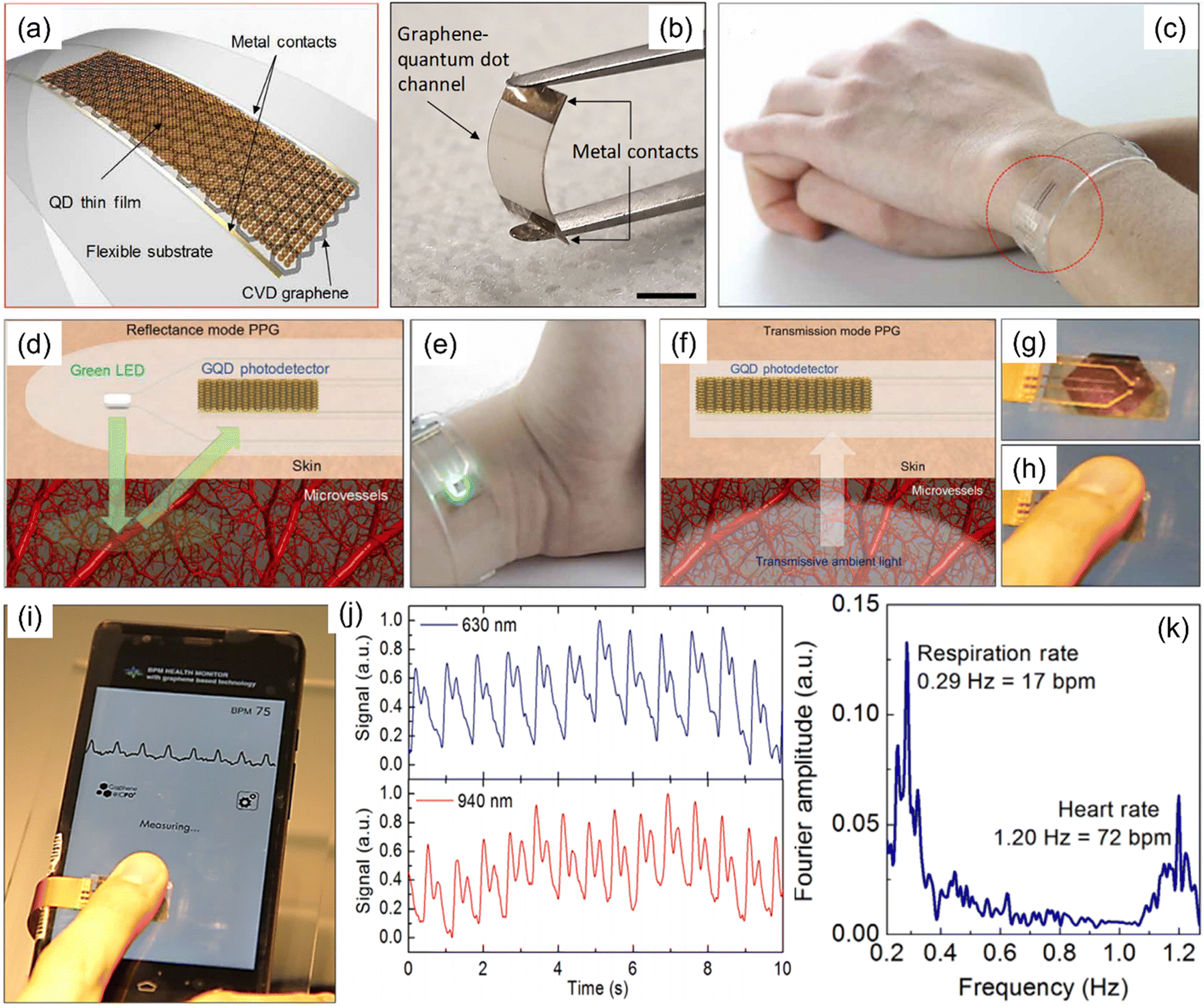 | ||
| Fig. 6 Wearable health monitoring application based on flexible GQD photodetectors. (a) Schematic diagram of a GQD photodetector integrated on a flexible substrate. (b) Photograph of a GQD photodetector on a PET substrate. Scale bar: 5 mm. (c) Photograph of a wearable GQD prototype device integrated on a wristband. (d) Schematic illustration of the reflectance mode for PPG. The change in the microvascular volume leads to variation in the intensity of the reflected light signal received by the GQD photodetector. (e) Photograph of the health monitoring wristband operated in reflectance mode. (f) Schematic illustration of the transmission mode for PPG. Ambient light as the light source passes through a finger and reaches the GQD photodetector on the other side. (g) and (h) Photographs of the GQD health patch operated in transmission mode. (i) Photograph showing the real-time monitoring of the PPG based on a GQD health patch paired with a mobile phone. (j) Typical PPG results extracted under 633 nm and 940 nm illuminations, respectively. (k) Fourier transformation of a PPG reading to extract the characteristic frequencies of HR and RR. The peaks located at 0.29 Hz and 1.20 Hz indicate the RR and HR of an individual. These frequencies correspond to a breathing rate of 17 breaths per minute and a heart rate of 72 beats per minute, respectively. Reproduced from ref. 104 with permission from American Association for the Advancement of Science, copyright 2019. | ||
Hemoglobin in erythrocyte plays an important physiological role in transporting oxygen by binding with O2. SpO2 serves as a vital clinical indicator for diagnosing diseases, especially hypoxemia. On account of the low absorption of red light and high absorption of infrared light, blood with high oxygenated hemoglobin levels appears distinctly bright red in color. In contrast, non-oxygenated hemoglobin commonly appears dark red, showing high absorption of red light and low absorption of infrared light. As a consequence, the difference in light absorption between oxygenated hemoglobin and non-oxygenated hemoglobin in the blood is comparatively significant at ≈633 nm and ≈940 nm (Fig. 6(j)). Consequently, the PPG reading under these two wavelengths is extracted to measure SpO2.
Due to the dynamic light absorption by blood and constant absorption by other biological tissues, the signal obtained from a PPG record can be divided into two parts: direct current (DC) signal and alternating current (AC) signal. The AC signal in PPG, which contains only the blood flow information, can be exploited for frequency analysis to obtain information about HR and RR by performing Fourier transformation. As shown in Fig. 6(k), the peaks at higher frequencies represent the inherent frequency of heartbeats, while the peaks at lower frequencies represent the RR manifested as a periodic modulation of heartbeats emanated from respiration. Moreover, a Bland-Altman plot analysis has been conducted by comparing this work with a clinically advanced PPG technology. A consistency correlation coefficient of 0.98 is extracted, demonstrating the high reliability of the GQD device.
Currently, in spite of the pioneering success, there is still much room for further improvement for the 2DLM photodetector-based health monitoring devices in term of accuracy, reliability, and application fields. Firstly, effectively separating the physiological signals from the environmental optical noise is still quite challenging, especially for the transmission working mode. In addition, most of the 2DLM based photodetectors suffer from a sub-linear photoresponse (i.e., small linear dynamics range).160,178 This will seriously curtail the accurate extraction of physiological information. In the future, machine learning algorithms can be exploited to improve the accuracy of signal reading. Furthermore, the linear dynamic range of 2DLM based photodetectors can be further extended through rational device design.179 Moreover, conventional 3D metal contacts have been used as the electrodes in this study, which will suffer from severe cracks/wrinkles after repeated bending treatments, leading to degenerated photosensitivity.180 Therefore, in the future, novel 2D electrodes such as Bi2Te3, VS2, NbS2, and PtBi2 can be integrated for further improving the flexibility.181–184 In the end, recent studies have shown that photodetectors can also be used to monitor the states of human organs, such as the extruded states.185 Further development is needed for the application of 2DLMs in this burgeoning field.
4. Target photoelectric tracking
Micro-area target photoelectric tracking is an emerging technology that utilizes photoelectric sensors and image processing technology to identify, monitor, and track the position and motion trajectory of tiny targets in real time. This technology usually exploits high-resolution photoelectric sensors to identify the motion of targets at the microscopic scale, and extracts the features and motion parameters through image processing algorithms. Micro-area target photoelectric tracking has a series of advantages such as high spatial resolution, non-destructive monitoring, as well as high speed, and this technique thus has potential application value in a variety of domains, including observation of microorganisms, handwriting recording, drug delivery, etc. In the past decade, 2DLMs have shown prominent advantages in high-speed and highly integrated optoelectronic devices due to their excellent compatibility with commercial micro/nano manufacturing techniques, ease of integration, strong light-harvesting capability, and high carrier mobility. Therefore, these newly emerged competitors have broad application prospects in the field of micro-area target photoelectric tracking. However, relevant research has still been relatively scarce in recent years.To this end, in 2020, Luo and collaborators prepared a γ-In2Se3/GaAs heterojunction photodetector array (1 × 10) and successfully exploited it for the trajectory tracking of a light spot.186 The preparation of the γ-In2Se3/GaAs photodetector array is achieved through patterning technique assisted magnetron sputtering deposition (Fig. 7(a)). Specifically, photolithography patterning process assisted selective-area solution etching technology is firstly used to prepare exposed GaAs windows on the Al2O3/GaAs substrate. Afterwards, magnetron sputtering deposition of a γ-In2Se3 thin film on the bare GaAs windows is carried out to construct the γ-In2Se3/GaAs heterojunctions. As confirmed by the sharp peaks of the X-ray diffraction pattern, the γ-In2Se3 nanofilm grown by magnetron sputtering exhibits relatively high crystallinity. By utilizing the photovoltaic effect, the γ-In2Se3/GaAs device can be operated under self-powered conditions, which greatly suppresses its dark current. Under 660 nm irradiation, the on/off ratio, responsivity, and detectivity reach 1.29 × 10⁴, 0.25 A W−1, and 7.34 × 10¹² Jones, respectively. More importantly, the device demonstrates a fast response rate with a response/recovery time of 23.6/146.7 µs (Fig. 7(b)). Meanwhile, the device array exhibits high uniformity with reliable device-to-device variation (Fig. 7(c)). The preceding characteristics have jointly provided the γ-In2Se3/GaAs heterojunction photodetector array with tremendous potential for application in micro-area target photoelectric tracking. The researchers have used this photodetector array for real-time tracking of a moving light spot. As shown in Fig. 7(d) and (e), the arrayed γ-In2Se3/GaAs sensing units respond sequentially to the light simulation, verifying their target motion tracking function.
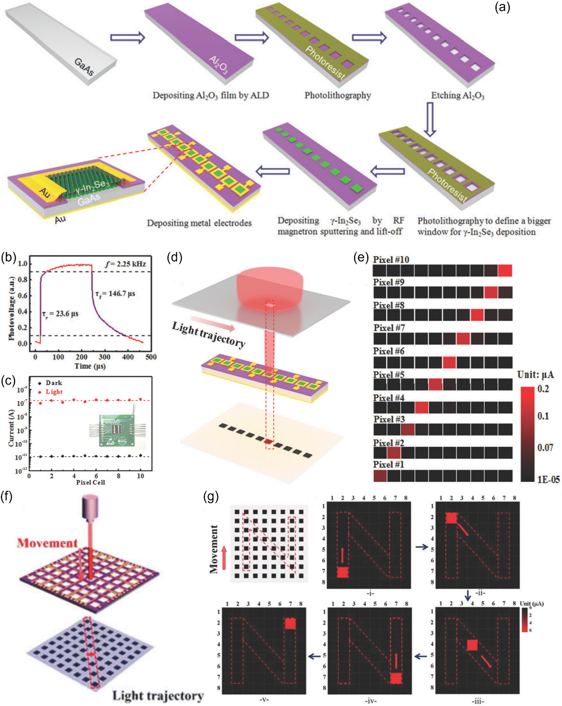 | ||
| Fig. 7 (a) Schematic illustration of the fabrication process for constructing the linear γ-In2Se3/GaAs heterojunction photodetector array. (b) The temporal photoresponse of a γ-In2Se3/GaAs photodetector. (c) The channel current in the dark and under illumination of the γ-In2Se3/GaAs heterojunction photodetectors in the array. (d) Schematic diagram of the real-time light spot trajectory tracking. (e) Variation of the photocurrent of each pixel when the light spot moves through the array. Reproduced from ref. 186 with permission from the Royal Society of Chemistry, copyright 2020. (f) Schematic diagram of the real-time light spot trajectory tracking based on a planar PtSe2/Si photodetector array. (g) Schematic diagram illustrating the light spot movement in an “N”-shaped trajectory and 2D current contrast maps showing the variation of the terminal current when the light spot moves through the array. Reproduced from ref. 187 with permission from Royal Society of Chemistry, copyright 2021. | ||
Due to the linear arrangement of the photoelectric sensor array in the above study, it can only be used to track the linear motion of the target. To address this deficiency, in a subsequent study, researchers from the same group have prepared a 8 × 8 PtSe2/Si heterojunction photodetector array.187 Importantly, the PtSe2/Si device manifests a short rise/decay time of 14.7/17.5 µs. Taking a step further, they use the planar device array to monitor the in-plane motion of a light spot and successfully achieve the monitoring of the “N” shape scanning trajectory (Fig. 7(f) and (g)), demonstrating the indisputable potency of 2DLM-based photodetectors in the field of micro-area target photoelectric tracking.
To date, the application and development of 2DLM based photodetectors in the field of photoelectric tracking of the micro-area target are still in the very initial stage. There are still a series of critical issues that need to be further addressed prior to their practical commercialization. On one hand, the spatial resolution of the optoelectronic target tracking system still needs to be further improved to enable more precise location and motion trajectory monitoring. On the other hand, as the preliminary exploration, the different device units in the above device arrays are electrically interconnected on account of the immature device design and manufacturing technology, which can result in undesirable crosstalk among different device units. To address the preceding issues, it is necessary to develop high-precision, non-destructive micro/nano processing technology for patterning 2DLMs and perform reasonable circuit design for signal readout in the upcoming future.
5. Optoelectronic logic operation
Optoelectronic logic devices combine photoelectric sensing and logic operations to achieve feature extraction and direct processing of incident optical information, significantly improving the efficiency of information identification and processing. These devices can markedly reduce the amount of data transmission and thus improve the response speed of the optoelectronic system. In addition, the development of optoelectronic logic devices will also promote the integration and innovation of optoelectronic technology, injecting new vitality into the domain of optoelectronics, which is of great significance for the progress of modern information technology. Profiting from the easy integration, excellent photosensitivity, and outstanding electrostatic controllability, 2DLM based photodetectors have shown considerable application prospects in the field of optoelectronic logic devices.In 2022, Yang et al. prepared a Gr/h-BN/MoS2 heterojunction photodetector with diverse photoresponse characteristics and achieved a series of reconfigurable non-volatile optoelectronic logic operations.188Fig. 8(a) shows the structure of the device, with MoS2 as the transport channel and Gr as the floating gate. As shown in Fig. 8(b), the transport state of the device can be significantly adjusted by the gate voltage pulse. When a negative gate pulse is applied, the device turns to the low-resistance state (erase state), since electrons are pushed from graphene to MoS2, leading to a positive float gate. When a positive gate pulse is applied, the device turns to a high-resistance state (program state), since electrons are driven from MoS2 to graphene, leading to a negative float gate. As shown in Fig. 8(c), the device exhibits a bipolar photoresponse, depending on the initial conduction state. Starting from the program state, the photoresponse is positive, since the photogenerated holes are driven from MoS2 to graphene. This will weaken the float-gate effect, and the channel current thus increases. In contrast, starting from the erase state, the photoresponse is negative, since the photogenerated electrons are driven from MoS2 to graphene. This will also weaken the float-gate effect, and the channel current thus decreases. Subsequently, the device is used as the core functional component of Boolean logic operations. Logic inputs are the gate voltage and incident light, and the logic output is the source–drain current. By setting different initial states and inputting different signals at the input ends, “AND”, “OR”, “NAND”, and “NOR” logic operations can be successfully achieved (Fig. 8(d)–(g)). Specifically, starting from the program state, neither small negative gate bias or weak light illumination can lead to a significant increase in the electrical conductance, whereas the simultaneous input can lead to a high output current, corresponding well to the “AND” logic function (Fig. 8(d)). Starting from the program state, either large negative gate bias or strong light illumination can lead to a significant increase in the electrical conductance, corresponding well to the “OR” logic function (Fig. 8(e)). Starting from the erase state, neither small positive gate bias or weak light illumination can lead to a significant decrease in the electrical conductance, whereas the simultaneous input can lead to low output current, corresponding well to the “NAND” logic function (Fig. 8(f)). Starting from the erase state, either large positive gate bias or strong light illumination can lead to a significant decrease in the electrical conductance, corresponding well to the “NOR” logic function (Fig. 8(g)). Overall, this study presents a flexible strategy for realizing multiple logic operations based on a single 2D vdWM photodetector with diverse photoresponse characteristics. Most recently, by using ultraviolet (UV) and blue illuminations as the input signals and using the SiC/graphene UV-visible dual-band photodetector as the sensing component, Zhang et al. have realized an “AND” optoelectronic logic gate, where the output signal is “1” only when both UV and visible illuminations are inputted.189
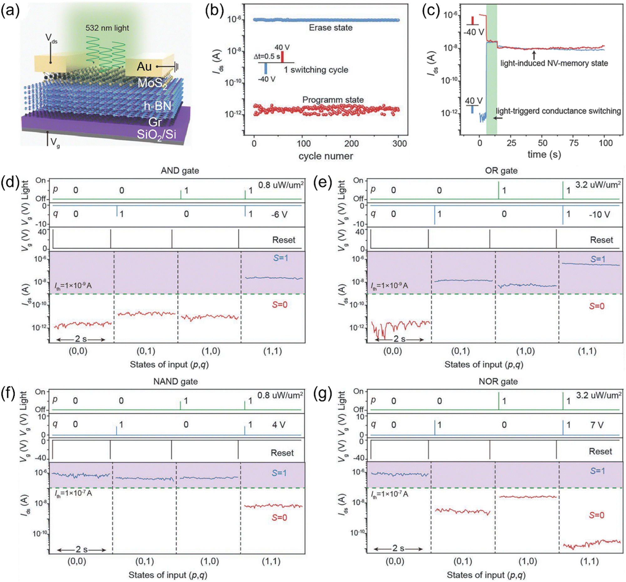 | ||
| Fig. 8 (a) 3D schematic diagram of a Gr/h-BN/MoS2 photodetector. (b) Program and erase states during multiple operation cycles. (c) Output current under various gate pulse and light pulse conditions. (d) AND, (e) OR, (f) NAND, and (g) NOR logic operations. Reproduced from ref. 188 with permission from John Wiley and Sons, Inc., copyright 2022. | ||
6. Ultraviolet monitoring
A radiation dosimeter is a kind of device that capitalizes on photoelectric conversion to monitor the surrounding radiation level. It is of great importance in a wealth of domains ranging from functional clothing, personal health, cosmetics, to medical treatment. Radiation dosimeter can remind people to prevent themselves from surrounding harmful radiation such as the fierce sunburn as well as X-ray in time, and thus help people avoid absorbing excessive radiation that can potentially damage their health. In the past decade, 2DLMs have demonstrated extensive advantages in radiation sensing, including high sensitivity, fast response rate, and ease of integration. In addition, the atomically thin nature of 2DLMs can endow the related optoelectronic devices with high transparency, excellent flexibility, and light weight, making them competitive in wearable devices. Accordingly, the photoelectric sensors made of 2DLMs are promising candidates for radiation monitoring.Lee et al. developed a real-time, wireless, and wearable UVA monitoring patch based on porous reduced graphene oxide (pRGO) paper in 2022.190 Compared to pristine graphene with a gapless band structure, the bandgap of reduced graphene oxide can be significantly opened,191 which can prevent the photocarriers from recombining in an efficient way. In addition, the bandgap can be widely manipulated from 1.0 eV to 3.5 eV through tuning the reduction level,192 providing a flexible approach to meet a targeted application. Impressively, the photocurrent of the pRGO paper photodetector largely remains invariable under both compressive and tensile bending treatments with a bending radius down to 2.0 mm (Fig. 9(a)). In addition, this pRGO device exhibits excellent anti-fatigue performance. Specifically, the photocurrent remains consistent even after 5000 bending cycles, as depicted in Fig. 9(b). As shown in Fig. 9(c), the distinct photoswitching characteristics has also been well maintained under bending operating conditions. This outstanding flexibility enables the pRGO devices to be flexibly integrated on various surfaces (Fig. 9(d)), without experiencing notable degradation in device properties, which substantially broadens the potential application scope in daily life. As such, the device has been further exploited for wearable real-time UVA monitoring. To achieve real-time and continuous ultraviolet radiation measurement, the device has been integrated with several components, including a flexible and bendable pRGO sensor, a microcontroller for real-time signal processing, a bluetooth module for wireless signal transmission, a lithium polymer battery for power supply, and a graphical user interface (GUI) designed to display and alert about the UV radiation levels (Fig. 9(e)). To validate the function, two sets of experiments have been conducted, one performed outdoors and the other in a synthetic laboratory under controlled exposure to ultraviolet radiation with a wavelength of 365 nm and an intensity of 27.9 mW cm−2. As shown in Fig. 9(f) and (g), real-time varying photocurrent reflecting the UVA level has been successfully recorded, verifying the outstanding UVA radiation monitoring capability of the pRGO patch.
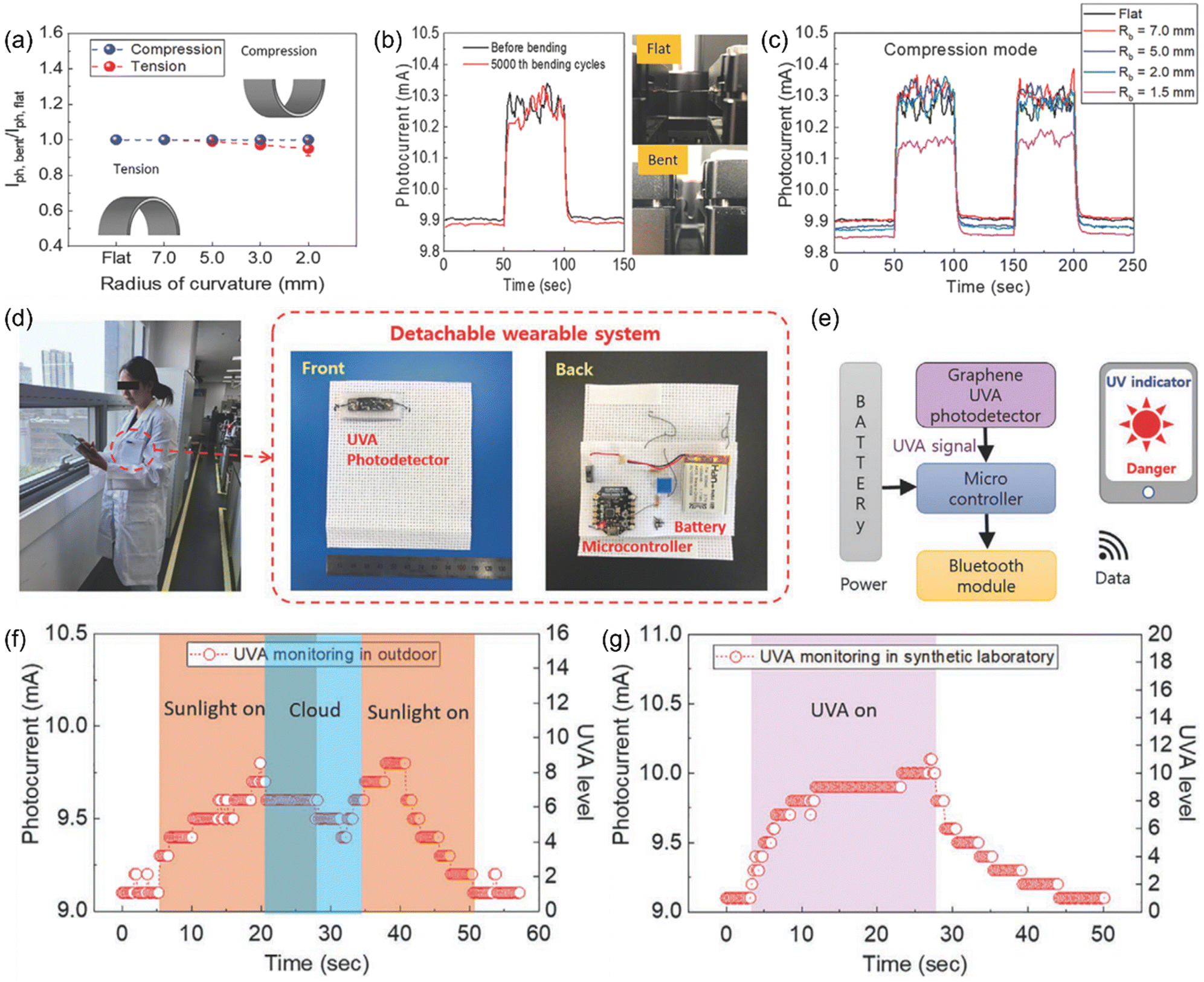 | ||
| Fig. 9 Flexible pRGO photodetector and its application in a UVA dosimeter. (a) Normalized photocurrent as a function of the bending curvature radius upon compressive strain (blue dots) and tensive strain (red dots). (b) Photoswitching curves before bending (black line) and after 5000 bending cycles (red line). (c) Photoswitching curves upon bending treatments with various bending radii. (d) Photograph of a wireless pRGO UVA monitoring system attached onto a researcher (left). Photographs of the front view and the rear view of the detachable wearable system (right). (e) Functional block diagram of the wearable pRGO system. (f) Real-time UVA levels measured outdoor. The orange region and blue region represent sunny and cloudy conditions, respectively. (g) Real-time UVA levels measured in an indoor synthetic laboratory. The pink region represents UVA on. Reproduced from ref. 190 with permission from John Wiley and Sons, Inc., copyright 2022. | ||
As the expensive and complex manufacturing processes such as photolithography, high-temperature treatment and etching have been circumvented, the above wearable UVA monitoring system is cost-effective. However, due to the presence of a lithium-polymer battery for the power supply, its volume and weight exceed those of many commercial portable systems. To solve this problem, Polat and collaborators have developed a UV skin exposure monitoring patch with a wireless power supply.104 Specifically, the UV monitoring patch has integrated a flexible ultraviolet-sensitive GQD photodetector with a commercially available flexible near-field communication (NFC) circuit board, allowing wireless transmission of both power and data between the photodetectors and a smartphone. This design ensures battery-free operation for sensing the environmental UV index. In addition, a flexible short-pass light filter has been specifically designed to block the undesired light spectrum (>400 nm) and offers extra protection against mechanical strain.
Presently, the development and application of 2DLM-based photodetectors in UV radiation monitoring are still in the very initial stage. Several critical issues need further research attention. Firstly, the use of active devices will significantly increase the volume and reduce their integration capability. Although the wireless power transmission strategy has been developed, additional power consumption emerges as a derivative problem due to the low conversion efficiency. In recent years, van der Waals heterostructures such as MoS2/WSe2,193 MoS2/AsP,194 and WSe2/graphene195 have been successfully developed as solar cells. In the upcoming future, these atomically thin solar cells can be used as the power sources for the radiation dosimeters to enable self-powered operation, which is conducive to further reducing the device's volume and weight. In addition, the previously reported devices have broadband photoresponse. Therefore, in practical application, light filters are commonly needed to isolate surrounding visible and infrared light to prevent false alarm. This will increase the complexity of device design and preparation. Of note, large-bandgap materials have an inherent anti-interference ability for visible and near-infrared light. Fortunately, there have emerged a series of large-bandgap photosensitive 2DLMs, including NiPS3,196 GeSe2,197α-MoO3,198 AsSbO3,199 GaPS4,200 and h-BN,201 which are promising candidates for filter-free UV radiation dosimeters in the future.
7. Optical communication
Optical communication is a modern communication mode that uses light waves as the medium for information transmission.202,203 The basic principle of optical communication is to convert the transmitted information into modulated optical signals, transmit them to the terminal through a medium such as optical fiber, and then convert the optical signals into electrical signals by the optical receiver, and finally restore them to the original information with the processor. Optical communication technology manifests a series of advantages, including low transmission loss, large transmission capacity, and strong resistance to electromagnetic interference, making it widely used in civil and military fields.Currently, the light-sensing components of the modern optical communication systems are being confronted with a wealth of predicaments. Firstly, with the rapid development of modern information technology, the transmission distance of optical communications is constantly increasing, which inevitably leads to the attenuation of optical signals and the increase of noise level. Therefore, higher sensitivity and signal-to-noise ratio have always been anticipated to achieve reliable information transmission over longer distance. Secondly, modern information technology has been putting forward increasingly high demands for communication capacity, requiring a higher bandwidth, which demands a higher response rate for light-sensing devices. In addition, the optical communication systems are commonly subject to various forms of extrinsic interference, which may lead to a decrease in the signal quality and an increase of the transmission error rate. Accordingly, the light-sensing components need to possess a stronger anti-interference ability. Furthermore, in practical applications, the light-sensing components should also have characteristics such as low cost, environmentally friendly composition, and long lifetime to ensure large-scale, distributed, long-term, and stable optical communications, which are difficult to achieve with traditional materials. To address the afore-mentioned challenges, it is thus impending to explore new optoelectronic sensing candidate materials.
In this context, Lei and collaborators recently prepared high-performance Ta2NiSe5/GaN heterojunction photodetectors (Fig. 10(a)) and successfully exploited them for proof-of-concept optical information transmission.204 Impressively, the on/off ratio of the device reaches ≈107, which is of great significance for achieving a low error rate. The optimal responsivity and detectivity reach 1.22 × 10⁴ A W−1 and 1.3 × 10¹⁶ Jones, respectively (Fig. 10(b)). Meanwhile, the response/recovery time is as short as 1.22/3.16 ms (Fig. 10(c)). Fig. 10(d) shows the typical experimental configuration of free space optical information transmission. In principle, the transmitted ASCII information is used to control the chopper, where “1” represents unblocked light and “0” represents blocked light. As a consequence, the generated light pulses will carry the required information for transmission. The light pulses are subsequently detected by the photodetector in the receiving end, generating two sets of states: high current state and low current state, representing “1” and “0” of the binary, respectively. After processing by the processor, the original information can be reproduced. As shown in Fig. 10(e), the Ta2NiSe5/GaN heterojunction photodetector has successfully achieved the accurate transmission of “LJP”, verifying the important potential of 2DLM based photodetectors in the optical communication industry.
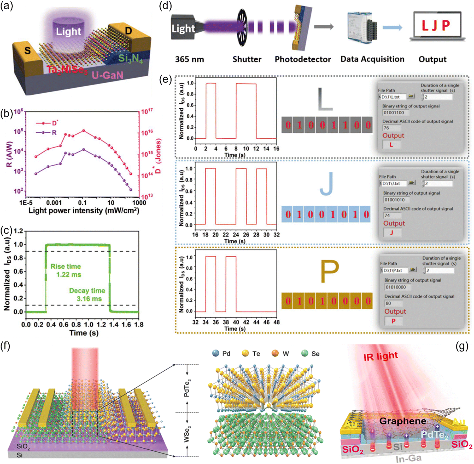 | ||
| Fig. 10 (a) 3D schematic diagram of a Ta2NiSe5/GaN heterojunction photodetector. (b) Responsivity and detectivity as a function of light power intensity. (c) Response rate. (d) Schematic illustration of the experimental configuration for optical communications. (e) Proof-of-concept application demonstrating the successful transmission of the ASCII code of “LJP”. Reproduced from ref. 204 with permission from Science China Press, copyright 2024. (f) 3D schematic diagram of a PdTe2/WSe2 heterojunction photodetector. Reproduced from ref. 205 with permission from John Wiley and Sons, Inc., copyright 2023. (g) 3D schematic diagram of a graphene/PdTe2/Si heterojunction photodetector. Reproduced from ref. 206 with permission from American Chemical Society, copyright 2023. | ||
As for practical applications, optical fibers have been extensively used as the transmission mediums for optical communications because of their large communication capacity, low transmission loss, strong resistance to electromagnetic interference, excellent confidentiality, rich source materials, light weight, and good flexibility. In fiber optic communications, the loss of optical signals during transmission in optical fibers is an imperative element to consider. Generally, the most suitable wavelengths for fiber optic communications are 850 nm, 1310 nm, and 1550 nm, where the transmission loss is the lowest and the transmission distance is thus the longest.207 However, the effective spectral window of many 2DLMs, such as the most commonly studied transition metal dichalcogenides (e.g., MoS2, WS2), cannot cover the most suitable wavelengths for the fiber optical communications mentioned above.208 Therefore, it is urgent to explore new 2DLMs that can respond to the infrared bands and exploit them for optical information transmission applications. To this end, Zhang et al. prepared PdTe2/WSe2 heterojunction photodetectors and achieved optical information communication applications at 850 nm and 1310 nm (Fig. 10(f)).205 Similarly, Zeng et al. prepared a graphene/PdTe2/Si heterojunction photodetector and successfully achieved optical information transmission at 1550 nm (Fig. 10(g)).206 Most recently, Xiong et al. constructed a β-In2Se3/Te broadband photodetector and harnessed it for optical communications at 1310 and 1550 nm.209
Although the above studies have achieved initial encouraging success, the high cost of the noble metal containing building blocks has severely hindered further large-scale practical applications. In recent years, a series of noble-element-free small-bandgap 2DLMs and their heterojunctions, such as black phosphorus,210 In1.75Sb0.25Se3,211 Sb2Te3,212 Bi2Se3,213 Bi2Te3/Si,214 WS2/Bi2Te3,215 WSe2/Bi2Te3,216 Bi2O2Se/Bi2Se3,217 MoS2/graphene/perovskite,218 and WSe2/Ta2NiSe5/WSe2,219 have been harnessed for infrared light sensing. These materials have enormous potential application value in the field of optical communications and they are worthy of further exploration in the upcoming future.
To this end, in 2023, Ye et al. constructed a high-temperature-resistant photodetector (Fig. 11(a)) by using a large-bandgap AgInP2S6 nanosheet as the photosensitive channel and successfully harnessed it for high-temperature optical communication.66 Research has found that AgInP2S6 photodetectors have excellent high-temperature resistance performance. Specifically, as the operating temperature increases from 24 °C to 160 °C, the device can maintain distinct optical switching characteristics (Fig. 11(b)). When the temperature returns to the initial temperature, the optical response of the device also roughly returns to the initial value. In addition, even when heated continuously at 150 °C for 10 hours, the device can still respond quickly and repetitively to periodically changing incident light (Fig. 11(c)). On this basis, the AgInP2S6 device was used as the optical signal receiving component to achieve the transmission of optical information at a working temperature of 160 °C. The obtained signal waveform is consistent with the results at room temperature (Fig. 11(d)).
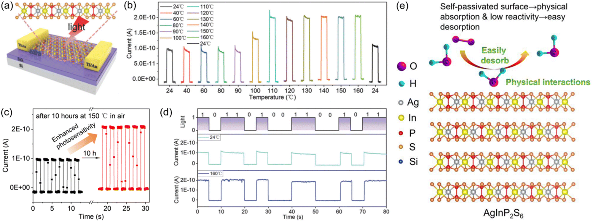 | ||
| Fig. 11 (a) 3D schematic diagram of a AgInP2S6 photodetector. (b) Photoswitching curves under various working temperatures (24 to 160 °C). (c) Photoswitching curves of the AgInP2S6 photodetector before and after 10-hours of heating treatment in air at 150 °C. (d) Results of optical communications by using the AgInP2S6 photodetector as a light signal receiver under 24 and 160 °C. (e) Schematic illustration of the high stability of AgInP2S6 against the ambient species enabled by the self-passivated surface. Reproduced from ref. 66 with permission from John Wiley and Sons, Inc., copyright 2023. | ||
The excellent immunity to high temperature of the AgInP2S6 devices is attributed to the synergy of multiple ingredients. Firstly, the bandgap of AgInP2S6 reaches ≈1.94 eV, which can significantly mitigate the intrinsic thermal excitation. Secondly, the covalent bonding between the atoms of AgInP2S6 is quite strong, which can suppress the decomposition caused by thermal disturbance. Finally, AgInP2S6 possesses a self-passivated surface, greatly suppressing its surface reactivity (Fig. 11(e)). On the whole, the above research has demonstrated that large-bandgap 2DLMs have enormous potential for application in high-temperature-proof optical communications. Thus far, researchers have discovered a series of large-bandgap 2DLMs, including InTeClO3,220 SnP2S6,55 and GeSe2.221 In the future, the resistance to high temperature of these candidate materials and their application in high-temperature optical communications will be in need of further exploration.
In addition to power intensity, propagating light also carries other information such as polarization state and phase. The identification of these additional degrees can be exploited to further improve the efficiency of optical information transmission.222,223 To this end, in 2022, Lu et al. prepared O–WS2/WS2 heterojunction photodetectors by using selective oxidation treatment, which was realized by e-beam lithography-assisted oxygen plasma irradiation.105 With the advantage of the lowered geometric symmetry, the O–WS2/WS2 device exhibits a distinct polarization-dependent photoresponse, where the photoresponse reaches the maximum/minimum value upon illumination with perpendicular (90°)/parallel (0°) polarization. On this basis, proof-of-concept multiplexing optical communication application has been proposed and achieved by using this O–WS2/WS2 device as the optical signal receiving component (Fig. 12(a)). Specifically, the light intensity and polarization state are simultaneously used as independent information transmission channels. Strong light represents “1” of the binary signal, and weak light represents “0”. In addition, perpendicular polarization represents “1”, and parallel polarization represents “0”. Since the output signal of the O–WS2/WS2 photodetector depends on both light intensity and polarization state, there are a total of four levels of output photocurrent when the binary signals are transmitted through the two channels, which are denoted as level “4”, level “3”, level “2”, and level “1” from high to low, corresponding to “strong light & perpendicular polarization”, “strong light & parallel polarization”, “weak light & perpendicular polarization”, and “weak light & parallel polarization”, respectively. In this study, the binary signal of “10101010” is used to program the light intensity, while a binary signal of “11011010” is used to program the polarization state (Fig. 12(b)). As shown in Fig. 12(c), the output photocurrent signal is “42324141”, which can be decoupled into “1010101011011010” as per the preceding established relationship (Fig. 12(d)), successfully transmitting 16 signals in 8 readout cycles. Most recently, Pan et al. achieved the transmission of 32 binary signals in 16 readout cycles by taking use of the anisotropy-enabled quaternary outputs of a polarization-resolved ReSe2/SnSe2 photodetector.170 On the whole, these studies provide new pathways for high-efficiency optical information transmission systems using 2DLM polarization-discriminating photodetectors as the light receiving components.
 | ||
| Fig. 12 (a) Schematic illustration of the mechanism for multiplexing optical communications. (b) Schematic illustration of the binary signals used for programming the light intensity and the polarization state. (c) The corresponding output current. (d) The decoupled binary signals according to the established relationship among output current, light intensity and polarization state. Reproduced from ref. 105 with permission from American Chemical Society, copyright 2022. | ||
Apart from the information transmission efficiency, another imperative consideration for optical communications is the confidentiality of the transmitted data. Optical communications, serving as one of the most popular ways of modern information transmission, will deal with a substantially large amount of sensitive and confidential information. If transmitted without encryption, the information can be easily wiretapped, which may cause severe security risks. Encryption technology can effectively warrant data confidentiality, ensuring that the information will not be illegally accessed during transmission.224 Therefore, encryption of optical communications plays an irreplaceable role in maintaining information security and ensuring communication reliability.
In 2023, Zhang et al. prepared a Gr/GaN heterojunction photodetector with a bipolar photoresponse (Fig. 13(a)) and demonstrated proof-of-concept encrypted optical communications by using this device as the light signal receiver.225 Impressively, upon UV illumination, the device exhibits a negative photoresponse, whereas the photoresponse becomes positive upon red light illumination. The working mechanism of the bipolar photoresponse can be well explained using energy band diagrams. As shown in Fig. 13(b), under UV irradiation, a large number of photoexcited electron–hole pairs are generated in GaN. Under the drive of the interfacial built-in electric field, electrons flow into graphene (p-type), thereby increasing its Fermi level and reducing its conductivity (i.e., giving rise to negative photoresponse). As shown in Fig. 13(c), under red light irradiation, intrinsic excitation can hardly occur, but electrons from the valence band can be excited to the mid-gap states. As the number of trapped electrons increases, the interfacial potential barrier decreases, and holes thus inject into graphene, thereby lowering its Fermi level and leading to a positive photoresponse. Subsequently, the bipolar Gr/GaN photodetector is further applied to encrypted optical communications. As shown in Fig. 13(d), the red light channel is used as the signal channel, while the ultraviolet light channel is used as the key channel. In the signal channel, interfering items will be inserted, which are labeled by the dark state of the key channel. As shown in Fig. 13(e), there are a total of four output modes depending on the two channels’ inputs, namely “00”, “01”, “10”, and “11”, corresponding to “Red off & UV on”, “Red on & UV on”, “Red off & UV off”, and “Red on & UV off”. Fig. 13(f) presents the output result. According to Fig. 13(e) and (f), the input signals of the signal channel and the key channel are “110010” and “100111”, respectively, resulting in an unencrypted signal of “1010” (Fig. 13(g)). On the whole, this study depicts a paradigm for the implementation of encrypted optical communications based on 2DLM photodetectors with a bipolar photoresponse.
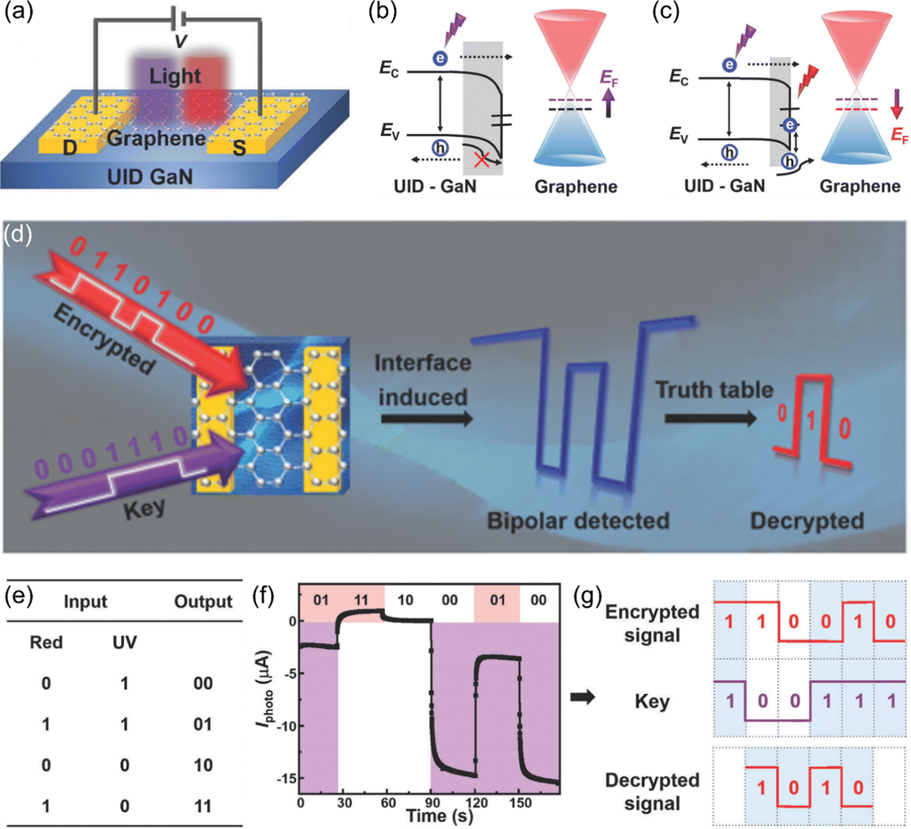 | ||
| Fig. 13 (a) 3D schematic diagram of the Gr/GaN photodetector. (b) and (c) Energy band diagrams of the Gr/GaN photodetector upon UV and red light illuminations, respectively. (d) Schematic illustration of the encrypted optical communications by using the bipolar Gr/GaN photodetector as the light receiver. (e) The one-to-one logical relationship between photocurrent levels and states of incident light. (f) The output photocurrent. (g) The decoupled channel signal, the key, as well as the decoded signal. Reproduced from ref. 225 with permission from John Wiley and Sons, Inc., copyright 2023. | ||
Another pivotal factor determining the potential for application in optical communications is the response rate. Thus far, the response time of the majority of 2DLM based photodetectors has still been relatively long, mostly in the millisecond to microsecond range, which is disadvantageous to the data transmission efficiency. Fortunately, device structure optimization has proven to be an effective strategy for improving response rate. For example, by constructing vertical Gr/WSe2/Gr photodetectors, Massicotte et al. achieved a response time as short as 5.5 ps.226 In another research work, by using graphene as the bottom electrode to enable vertical carrier transport, Dai et al. increased the response rate of the Au/InSe Schottky junction photodetector by approximate three orders of magnitude.227 In the future, more device optimization schemes should be designed to accelerate the transport and collection of photocarriers, finally shortening the response time of various 2DLM based photodetectors.
8. Automatic driving
Automatic driving is an emerging intelligent technology that capitalizes on advanced sensing systems and image processing algorithms to achieve unmanned operation. Lidar is one of the core components of automatic driving technology, which is a device that uses laser beams to identify targets. Basically, when an emitted laser beam is irradiated on a target, some of the light will be reflected. The light receiver detects the reflected light signal and restores it to an electrical signal. Through signal processing, various information about the target, including distance, motion direction, speed, shape, etc., can be obtained. In this consideration, photodetectors are the core components of LiDAR, serving as the “eyes”. Currently, the light-sensing components of LiDAR has been facing a series of tricky challenges, including large volume, low sensitivity, and high cost. Therefore, it is urgent to explore new potential materials. 2DLMs have the advantages of thin thickness, light weight, and strong interaction with light, thus manifesting important application potential in LiDAR next-generation technology.As a pioneering attempt, in 2023, Luo et al. prepared a high-performance WSe2/WS2/WSe2 dual-junction phototransistor (Fig. 14(a)) and successfully implemented an automatic driving function by exploiting it as the light signal receiver.228 The optimal responsivity and detectivity of the device reached 35.4 A W−1 and 1.9 × 10¹⁴ Jones, respectively (Fig. 14(b)). In addition, the response/recovery time of the device is as short as 3.2/2.5 ms (Fig. 14(c)). Further investigation has determined that the device can accurately identify light signals reflected back from different distances. As shown in Fig. 14(d), as the reflection distance decreases, the photoresponse gradually increases, laying a solid foundation for recognizing the distance of the target. Finally, the WSe2/WS2/WSe2 photodetector is used as an optical signal receiver for LiDAR and successfully implements the proof-of-concept automatic braking function (Fig. 14(e) and (f)). In a subsequent research work, the same research group has used an In2Se3/h-BN/CsPb(Br/I)3 heterostructure photodetector as the optical signal sensing component to achieve the proof-of-concept automatic obstacle avoidance function.229 The preceding studies have fully portended the enormous potential of 2DLM based photodetectors in automatic driving applications.
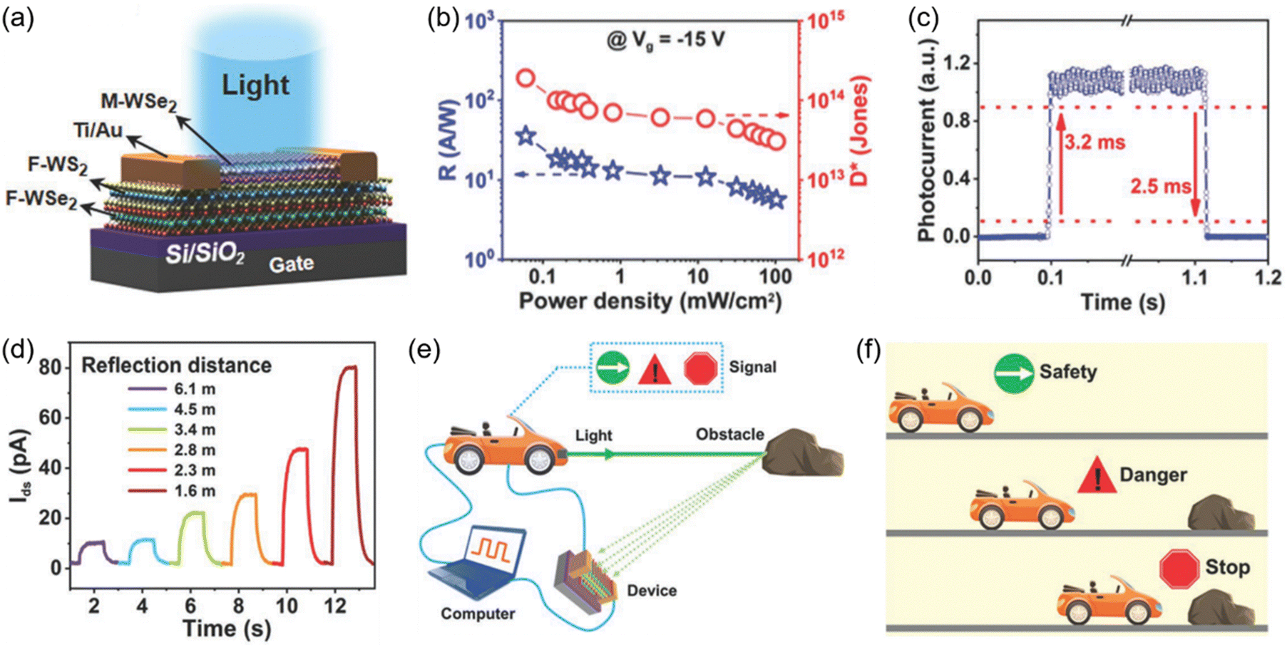 | ||
| Fig. 14 (a) 3D schematic diagram of a WSe2/WS2/WSe2 dual-junction photodetector. (b) Responsivity and detectivity as a function of light power density. (c) Temporal photoresponse. (d) Photoswitching curves upon illumination with various reflectance distances. (e) and (f) Schematic illustration on the working principle of the automatic driving system by using the WSe2/WS2/WSe2 photodetector as the light signal receiver. Reproduced from ref. 228 with permission from John Wiley and Sons, Inc., copyright 2022. | ||
Nevertheless, the above-mentioned studies have mainly focused on the visible band. In practical applications, infrared lights (e.g., 905 nm,230 1550 nm231) are much more favorable. On one hand, infrared light will not interfere with human vision. Meanwhile, it causes little radiation damage to the human eye. On the other hand, it has an excellent anti-interference ability and can accurately capture and measure targeted objects in complex environments (e.g., foggy day, hazy day). In the future, more research efforts should be focused on intelligent driving technology using 2DLM based infrared photodetectors as the optical signal sensing units.
9. Acoustic signal detection
Voiceprint detection is a technique that utilizes individual features contained in voice signals for identity recognition. The acoustic characteristics of each individual are unique, because there are slight differences in their vocal organs and language habits, which can lead to changes in the airflow of their voice, thereby resulting in differences in sound quality and timbre. Voiceprint detection has potential application value in a variety of critical fields, such as information security and non-contact control, which can improve security and efficiency, and promote the development of social informatization and intelligence. Recently, the perception of acoustic vibrations through light sensing has been demonstrated, especially using invisible light to augment detection confidentiality. This approach has significant advantages. For example, it offers a unique opportunity for amalgamating the detection process of visual and auditory stimuli. Compared with other commonly used devices, such as capacitive sensors and piezoelectric sensors, photodetectors prepared with 2DLMs have a higher response speed.Most recently, Fu et al. designed a vertically stacked graphene/Ge (Gr/Ge) hybrid field-effect phototransistor and harnessed it for the acquisition and modulation of auditory signals.232 By controlling the gate voltage, the interplay of source–drain current (Ids) and gate leakage current (Ig) in this device results in continuously tunable positive photocurrent (PPC) and negative photocurrent (NPC). As shown in Fig. 15(a), when the gate voltage falls below the threshold voltage, the Gr/Ge heterojunction appears to be forward-biased. In this case, the graphene channel and the Gr/Ge junction can be regarded as two resistors. When the device is illuminated, photocarriers are generated, reducing their resistance. Since the directions of Ids and Ig are consistent, the two flows will cooperate with each other to generate PPC. In contrast, when Vbg > Vth, the Gr/Ge junction is reverse-biased. Under illumination, the graphene's resistance is reduced and the heterojunction depletion layer is shrunk. Therefore, the Gr/Ge junction becomes a low-resistance resistor, and Ids and Ig are opposite. As a result, the two flows will compete with each other to produce NPC. Following the realization of the tunable photoresponse, the Gr/Ge hybrid field-effect phototransistor is used to detect auditory signal by leveraging the high responsivity and fast response speed. The experimental configuration is schematically shown in Fig. 15(b). A 1550 nm laser beam is directed onto a reflector in front of the sound source, after which it is reflected and detected by the Gr/Ge field-effect phototransistor. In principle, the acquisition and recording of the voice signal are realized by adjusting the laser's path. When the acoustic pressure interacts with the reflective mirror, it will make it move. The reflected light's position and the energy reaching the active area of the photodetector change accordingly (Fig. 15(c)). Consequently, the output photocurrent changes, recording the “shape” of the corresponding sound waves. Fig. 15(d) and (e) present the note signals captured by the Gr/Ge field-effect phototransistor at different gate voltages. Apparently, different notes generate different shapes of the I–t signals, laying a solid foundation for voiceprint detection. More importantly, the signal intensity recorded at a gate voltage of –1 V is higher than that recorded at +2 V, demonstrating the capacity of gate voltage modulation to amplify or attenuate sound waves, resembling the regulation mechanism of the human auditory system. On the whole, this study depicts an attractive paradigm for realizing voiceprint detection based on 2DLM photodetectors.
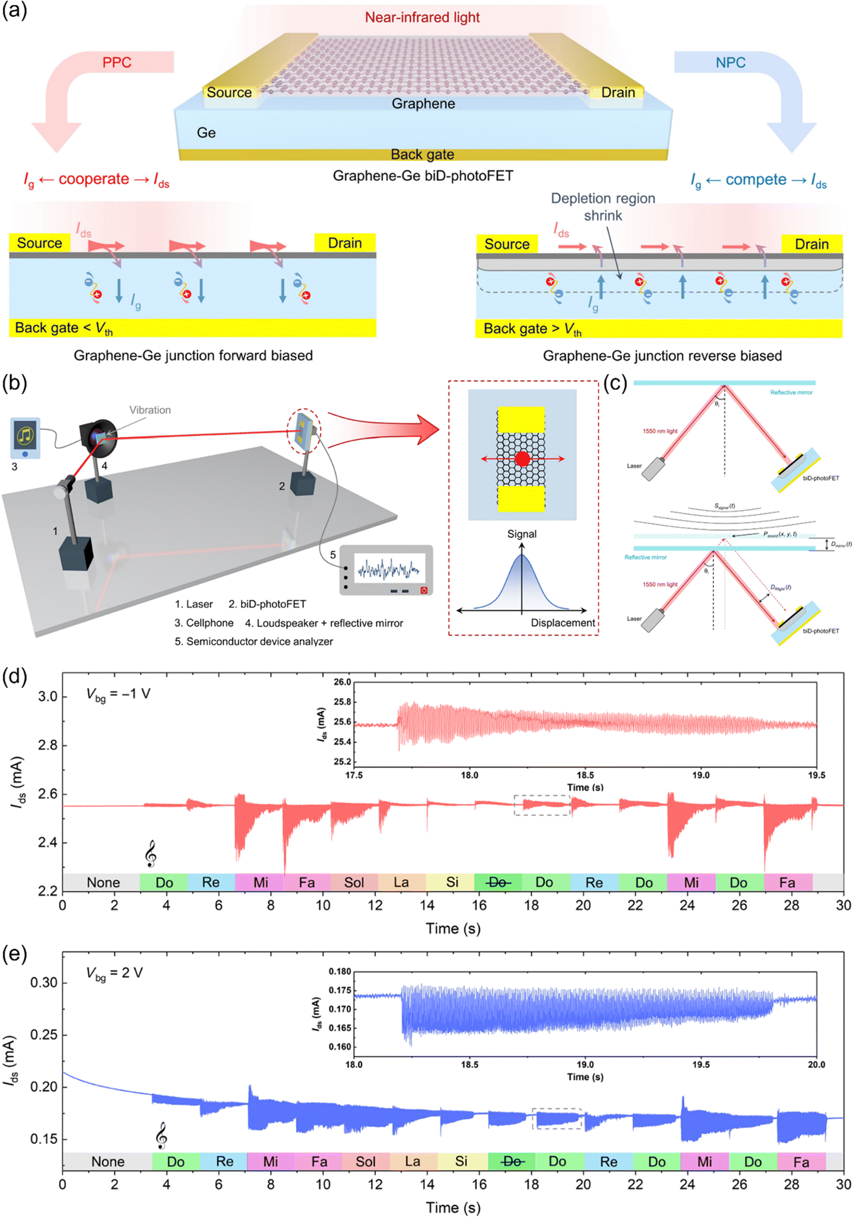 | ||
| Fig. 15 (a) Schematic illustration of the device structure of a Gr/Ge hybrid field-effect phototransistor and its working mechanism. (b) Schematic illustration of the measurement configuration for acoustic signal detection. (c) Schematic illustration of the effect of the acoustic wave on the optical signal reaching the device. (d) and (e) Output current without no acoustic input and with various acoustic inputs under the back gate voltage of –1 V and 2 V. Reproduced from ref. 232 with permission from American Chemical Society, copyright 2024. | ||
10. Conclusion & perspective
In summary, benefiting from the unique properties spanning excellent flexibility, pronounced electrostatic tunability, diversified electronic band structures, dangling-bond-free surface, and ease of integration, a wealth of research advancements have been accomplished in the field of optoelectronic applications by leveraging 2DLM photodetectors. To date, these devices have been widely applied in a variety of fields such as imaging, health monitoring, target tracking, optoelectronic logic operation, ultraviolet monitoring, optical communications, automatic driving, and acoustic signal detection, revealing enormous potential towards the next generation of photodetection. However, in the current stage, there are still some critical issues to be addressed, which have been epitomized below, along with the potential solutions addressing them.(A) One important ingredient restricting the further development of optoelectronic applications based on 2DLMs is their relatively poor photosensitivity. On account of the atomically thin thickness of 2DLMs, their light absorption is rather low, and their carrier lifetime is quite short. These together lead to the overall low photosensitivity of 2DLM photodetectors. Therefore, in the future, two approaches can be exploited to further improve the photosensitivity of 2DLM photodetectors. On the one hand, 2DLM photodetectors can be coupled with a plasmonic optical antennas/resonant metasurface to achieve localization of light through plasmonic resonance, thereby enhancing the interactions between 2DLMs and light.208,233 On the other hand, built-in electric fields or type II band arrangements can be introduced through band engineering and construction of heterostructures to extend the lifetime of photocarriers.234–236
(B) Another pivotal ingredient standing in the way of further development lies in the difficulty of scalable preparation of high-quality 2DLMs. Thus far, many exploratory studies on downstream optoelectronic applications have been conducted based on mechanical exfoliation technology.66,105,137 However, mechanical exfoliation technology usually only produces 2D nanosheets with a lateral scale of tens of micrometers, and its production yield is extremely low, and is far from meeting the needs of practical production and commercialization. Accordingly, there is an urgent demand to search for alternative preparation approaches. In view of this, MOCVD,237 MBE,238 CVD,239 and PLD153 can be potential approaches to overcoming this challenge.
(C) Although a variety of downstream applications have been realized using 2DLM photodetectors, the optoelectronics industry is an enormous industry. There are still extensive fields to be explored, such as wearable X-ray radiometers, bionic navigation, guidance, space exploration, etc.
As a concluding remark, photodetectors built of 2DLMs have demonstrated indisputable potential in a variety of optoelectronic devices. Although the prototype photodetectors have been widely explored, the investigation on the upcoming downstream applications is still in the early stage. There are still critical issues to be addressed. Looking ahead, by overcoming the existing challenges, it is envisioned that 2DLM photodetectors will play an imperative role in promoting the next-generation optoelectronic industry.
Data availability
No primary research results, software or code have been included and no new data were generated or analysed as part of this review.Conflicts of interest
The authors declare no competing interests.Acknowledgements
This work is supported by the National Natural Science Foundation of China (Grant No. 52272175, U2001215), the Natural Science Foundation of Guangdong Province (Grant No. 2021A1515110403, 2022A1515011487), the Science and Technology Projects in Guangzhou (Grant No. 202201011232), the One-Hundred Talents Program of Sun Yat-sen University, and the State Key Laboratory of Optoelectronic Materials and Technologies (Sun Yat-sen University).References
- Z. Li, T. Yan and X. Fang, Nat. Rev. Mater., 2023, 8, 587–603 CrossRef.
- Z. Zheng, J. Yao, J. Li and G. Yang, Mater. Horiz., 2020, 7, 2185–2207 RSC.
- H. Lu, W. Wu, Z. He, X. Han and C. Pan, Nanoscale Horiz., 2023, 8, 1014–1033 RSC.
- T. Araki, K. Li, D. Suzuki, T. Abe, R. Kawabata, T. Uemura, S. Izumi, S. Tsuruta, N. Terasaki, Y. Kawano and T. Sekitani, Adv. Mater., 2023, 36, 2304048 CrossRef PubMed.
- L. Li and G. Shen, Mater. Horiz., 2023, 10, 5457–5473 RSC.
- N. Zhang, X. Gao, H. Guan, S. Sun, J. Liu, Z. Shao, Q. Gao, Y. Zhang, R. Sun, G. Yang, F. Gao and W. Feng, Nano Res., 2024, 17, 4471–4477 CrossRef CAS.
- M. Kumar and H. Seo, Adv. Opt. Mater., 2023, 11, 2301165 CrossRef CAS.
- M. Deng, Z. Li, X. Deng, Y. Hu and X. Fang, J. Mater. Sci. Technol., 2023, 164, 150–159 CrossRef CAS.
- Y. Wang, L. Peng, J. Schreier, Y. Bi, A. Black, A. Malla, S. Goossens and G. Konstantatos, Nat. Photonics, 2024, 18, 236–242 CrossRef CAS.
- X. Cai, H. Zhang, P. Wei, Q. Liu, D. Sheng, Z. Li, B. Zhang, G. Tang, W. Zhao, Z. Ye, Z. Xue, Y. Xie, Y. Dai, C. Wang, Y. Wang, X. Fu, L. Yin, H. Peng, H. Ding, G. Zhao and X. Sheng, Nat. Photonics, 2024, 18, 492–500 CrossRef CAS.
- P. Wang, W. Xue, W. Ci, R. Yang and X. Xu, Mater. Futures, 2023, 2, 035301 CrossRef CAS.
- J. Qi, Z. Wu, W. Wang, K. Bao, L. Wang, J. Wu, C. Ke, Y. Xu and Q. He, Int. J. Extreme Manuf., 2023, 5, 022007 CrossRef.
- K. Cho, T. Lee and S. Chung, Nanoscale Horiz., 2022, 7, 1161–1176 RSC.
- X. Hang, X. Shengjie, X. Xun, Z. Jincheng, H. Weichang and D. Yi, Microstructures, 2022, 2, 2022011 CrossRef.
- H. Xue, W. Gao, J. Gao, G. F. Schneider, C. Wang and W. Fu, Int. J. Extreme Manuf., 2023, 5, 032010 CrossRef.
- A. Mondal and M. De, Tungsten, 2024, 6, 1–16 CrossRef.
- J. Han, F. Wang, Y. Zhang, W. Deng, M. Dai, F. Hu, W. Chen, J. Cui, C. Zhang, S. Zhu, C. Wang, M. Ye, S. Han, Y. Luo, T. Zhai, J. Wang and Q. J. Wang, Adv. Mater., 2023, 35, 2305594 CrossRef CAS PubMed.
- Q. Ye, J. Lu, H. Yi, Z. Zheng, C. Ma, C. Du, Y. Zou, J. Yao and G. Yang, Appl. Phys. Lett., 2022, 120, 181104 CrossRef CAS.
- P. Chen, L. Pi, Z. Li, H. Wang, X. Xu, D. Li, X. Zhou and T. Zhai, Appl. Phys. Lett, 2022, 121, 021103 CrossRef CAS.
- H. Zhang, Z. Wang, J. Chen, C. Tan, S. Yin, H. Zhang, S. Wang, Q. Qin and L. Li, Nanoscale, 2022, 14, 16130–16138 RSC.
- S. Yang, P. Luo, F. Wang, T. Liu, Y. Zhao, Y. Ma, H. Li and T. Zhai, Small, 2022, 18, 2105211 CrossRef CAS PubMed.
- S. Wang, Y. Bai, M. Liu, X. Zong, W. Wang, Q. Mu, T. Han, F. Li, S. Wang, L. Shan and M. Long, Nanoscale, 2023, 15, 17006–17013 RSC.
- Q. Zhang, B. Zhao, S. Hu, R. Tian, C. Li, L. Fang, Y. Zhang, Y. Liu, J. Zhao and X. Gan, Nanoscale, 2023, 15, 15761–15767 RSC.
- H. Mu, R. Zhuang, N. Cui, S. Cai, W. Yu, J. Yuan, J. Zhang, H. Liu, L. Mei, X. He, Z. Mei, G. Zhang, Q. Bao and S. Lin, ACS Nano, 2023, 17, 21317–21327 CrossRef PubMed.
- X. Cao, S. Yan, Z. Li, Z. Fang, L. Wang, X. Liu, Z. Chen, H. Lei and X. Zhang, J. Phys. Chem. Lett., 2023, 14, 11529–11535 CrossRef CAS PubMed.
- D. P. Do, C. Hong, V. Q. Bui, T. H. Pham, S. Seo, V. D. Do, T. L. Phan, K. M. Tran, S. Haldar, B. Ahn, S. C. Lim, W. J. Yu, S. G. Kim, J. H. Kim and H. Lee, Adv. Sci., 2023, 10, 2300925 CrossRef CAS PubMed.
- H. Yi, H. Yang, C. Ma, Y. Ma, Q. Ye, J. Lu, W. Wang, Z. Zheng, Z. Deng, Y. Zou, J. Yao and G. Yang, Sci. China Mater., 2023, 66, 1879–1890 CrossRef CAS.
- Y. Wang, W. Zhai, Y. Ren, Q. Zhang, Y. Yao, S. Li, Q. Yang, X. Zhou, Z. Li, B. Chi, J. Liang, Z. He, L. Gu and H. Zhang, Adv. Mater., 2023, 36, 2307269 CrossRef PubMed.
- H. Wang, Y. Li, P. Gao, J. Wang, X. Meng, Y. Hu, J. Yang, Z. Huang, W. Gao, Z. Zheng, Z. Wei, J. Li and N. Huo, Adv. Mater., 2023, 36, 2309371 CrossRef PubMed.
- S. Li, J. Zhang, L. Zhu, K. Zhang, W. Gao, J. Li and N. Huo, Adv. Funct. Mater., 2023, 33, 2210268 CrossRef CAS.
- M. Jiang, T. Zheng, J. Zhang, Z. Li, Q. Deng, Y. Pan, W. Gao, Y. Yang, J. Li and N. Huo, Adv. Opt. Mater., 2024, 12, 2303217 CrossRef CAS.
- S. Xiao, T. Zheng, W. Chen, J. Zhang, M. Yang, Y. Sun, Z. Zheng, D. Hao, N. Huo, Z. Chen and W. Gao, Adv. Funct. Mater., 2024, 2403509 CrossRef.
- M. R. Lien, N. Wang, J. Wu, A. Soibel, S. D. Gunapala, H. Wang and M. L. Povinelli, Nano Lett., 2022, 22, 8704–8710 CrossRef CAS PubMed.
- S. M. Koepfli, M. Baumann, Y. Koyaz, R. Gadola, A. Güngör, K. Keller, Y. Horst, S. Nashashibi, R. Schwanninger, M. Doderer, E. Passerini, Y. Fedoryshyn and J. Leuthold, Science, 2023, 380, 1169–1174 CrossRef CAS PubMed.
- J. Xue, S. Wang, J. Zhou, Q. Li, Z. Zhou, Q. Hui, Y. Hu, Z. Zhou, Z. Feng, Q. Yan, Y. Yu, Y. Weng, R. Tang, X. Su, Y. Xin, F. Zheng, S. Ju, L. You and L. Fang, Appl. Phys. Lett, 2023, 122, 181903 CrossRef CAS.
- M. Huang, M. Wang, C. Chen, Z. Ma, X. Li, J. Han and Y. Wu, Adv. Mater., 2016, 28, 3481–3485 CrossRef CAS PubMed.
- M. Yang, W. Gao, Q. Song, Y. Zhou, L. Huang, Z. Zheng, Y. Zhao, J. Yao and J. Li, Adv. Opt. Mater., 2021, 9, 2100450 CrossRef CAS.
- X. Guo, Y. Wang, A. Elbourne, A. Mazumder, C. K. Nguyen, V. Krishnamurthi, J. Yu, P. C. Sherrell, T. Daeneke, S. Walia, Y. Li and A. Zavabeti, Nanoscale, 2022, 14, 6802–6810 RSC.
- H. Jang, Y. Song, Y. Seok, H. Im, T. H. Kim, J. H. Lee, Y. H. Kim and K. Lee, Nanoscale, 2022, 14, 3004–3012 RSC.
- C. C. S. Maria, P. H. Wu, D. P. Hasibuan, C. S. Saragih, H. Giap, D. H. Nguyen, Y. R. Chen, R. A. Patil, D. V. Pham, J. L. Shen, C. C. Lai, M. K. Wu and Y. R. Ma, J. Mater. Chem. C, 2023, 11, 14316–14325 RSC.
- J. Chen, S. Lu, Y. Hu, F. Yang, H. Han, L. Kong, B. He, S. Ruan and B. Xiang, Adv. Opt. Mater., 2024, 12, 2301543 CrossRef CAS.
- X. Li, X. Chen, S. Li, F. Chu, W. Deng, X. Zhang, J. Li, X. Bao, B. An, C. You, F. Liu and Y. Zhang, Nanoscale, 2021, 13, 16448–16456 RSC.
- Y. Yang, J. Li, S. Choi, S. Jeon, J. H. Cho, B. H. Lee and S. Lee, Appl. Phys. Lett, 2021, 118, 013103 CrossRef CAS.
- M. Yang, Z. Luo, W. Gao, M. Zhang, L. Huang, Y. Zhao, J. Yao, F. Wu, J. Li and Z. Zheng, Adv. Opt. Mater., 2022, 10, 2200717 CrossRef CAS.
- Z. Muhammad, F. Wali, G. Hussain, R. Islam, S. Ullah, P. Wu, F. Khan, C. Autieri, Y. Zhang, T. Alshahrani and W. Zhao, J. Mater. Chem. C, 2023, 11, 2608–2618 RSC.
- M. Jiang, X. Pan, K. Zhang, S. Tian, L. Zhang, L. Han, Y. He, X. Lv, S. Lan, H. Xing and L. Wang, Adv. Electron. Mater., 2024, 10, 2300742 CrossRef CAS.
- Z. Zhao, F. Dong, Y. Wang, J. Sun, H. Ye, R. Wang and J. Zhang, Nanoscale, 2023, 15, 11955–11962 RSC.
- Y. Yu, M. Peng, F. Zhong, Z. Wang, X. Ge, H. Chen, J. Guo, Y. Wang, Y. Chen, T. Xu, T. Zhao, T. He, K. Zhang, F. Wu, C. Chen, J. Dai and W. Hu, Mater. Horiz., 2023, 10, 2579–2586 RSC.
- Y. Tian, Y. Cheng, J. Huang, S. Zhang, H. Dong, G. Wang, J. Chen, J. Wu, Z. Yin and X. Zhang, Nano Res., 2022, 15, 6628–6635 CrossRef CAS.
- S. Zhang, Y. Hao, F. Gao, X. Wu, S. Hao, M. Qiu, X. Zheng, Y. Wei and G. Hao, 2D Mater., 2024, 11, 015007 CrossRef.
- B. Sun, Z. Wang, Z. Liu, X. Tan, X. Liu, T. Shi, J. Zhou and G. Liao, Adv. Funct. Mater., 2019, 29, 1900541 CrossRef.
- L. Chen, C. Yang and C. Yan, J. Mater. Sci. Technol., 2020, 48, 100–104 CrossRef CAS.
- H. Zhao, Y. Yan, X. Song, Z. Ma, T. Tian, Y. Jiang, X. Li, C. Xia and J. Li, Nanoscale, 2021, 13, 3757–3766 RSC.
- C. Li, J. Wu, R. Bian, G. Cao, E. Pan, Z. Liu, J. Yu, H. Hosono and F. Liu, Adv. Funct. Mater., 2022, 32, 2208531 CrossRef CAS.
- Y. Zhang, F. Wang, X. Zhao, X. Feng, N. Zhang, F. Xia, Y. Ma, H. Li and T. Zhai, Nanoscale Horiz., 2023, 8, 108–117 RSC.
- Q. Hao, H. Yi, J. Liu, Y. Wang, J. Chen, X. Yin, C. S. Tang, D. Qi, H. Gan, A. T. S. Wee, Y. Chai and W. Zhang, Adv. Opt. Mater., 2022, 10, 2200063 CrossRef CAS.
- Q. Ye, J. Lu, Z. Zheng, W. Huang, J. Yao and G. Yang, Adv. Opt. Mater., 2022, 10, 2102335 CrossRef CAS.
- L. Xu, M. Yang, Q. Lu, Y. Ren, Y. Chen, J. Guo, M. Cai, X. Miao, F. Teng, H. Fan, C. Zhang, X. He and P. Hu, Phys. Status Solidi RRL, 2024, 18, 2300183 CrossRef CAS.
- M. Serra, N. Antonatos, J. Luxa, L. Lajaunie, J. Albero, A. Sabik, W. M. Linhart, H. Garcia, R. Kudrawiec, D. Sedmidubský and Z. Sofer, J. Mater. Chem. C, 2023, 11, 6317–6326 RSC.
- Y. Yang, J. Liu, C. Zhao, Q. Liang, W. Dong, J. Shi, P. Wang, D. Kong, L. Lv, L. Jia, D. Wang, S. Zheng, M. Wang, F. Liu, P. Yu, W. Ji, C. Huang, J. Qiao and J. Zhou, Adv. Mater., 2024, 36, 2307237 CrossRef CAS PubMed.
- L. Zhang, Y. He, X. Dong, J. Guo, Z. Gao, Z. Liu, J. Chen, Y. Zhao, Z. Zhou, J. Yin, X. Fu, F. Luo, H. Fu and J. Wu, Laser Photonics Rev., 2024, 18, 2300854 CrossRef CAS.
- X. Meng, Y. Du, W. Wu, N. B. Joseph, X. Deng, J. Wang, J. Ma, Z. Shi, B. Liu, Y. Ma, F. Yue, N. Zhong, P. H. Xiang, C. Zhang, C. G. Duan, A. Narayan, Z. Sun, J. Chu and X. Yuan, Adv. Sci., 2023, 10, 2300413 CrossRef CAS PubMed.
- T. Guo, Z. Sa, P. Wei, Y. Jian, X. Chen, Z. Chen, J. Avila, P. Dudin, Z. Yang, X. Song, F. Liu and S. Zhang, 2D Mater., 2023, 10, 025004 CrossRef.
- N. Q. Diep, Y. X. Chen, D. L. Nguyen, M. N. Duong, S. K. Wu, C. W. Liu, H. C. Wen, W. C. Chou, J. Y. Juang, Y. J. Hsu, V. Q. Le, Y. H. Chu and S. H. Huynh, J. Mater. Chem. C, 2023, 11, 1772–1781 RSC.
- Q. Li, S. Wang, J. Xue, Z. Zhou, Y. Hu, Z. Zhou, Z. Feng, Q. Yan, Y. Yu, Y. Weng, R. Tang, X. Su, F. Zheng, L. Fang and L. You, Phys. Rev. Appl., 2023, 19, 054055 CrossRef CAS.
- Q. Ye, Z. Deng, H. Yi, W. Wang, J. Lu, Y. Ma, W. Huang, Z. Zheng, C. Ma, C. Du, Y. Zou, J. Yao and G. Yang, Adv. Opt. Mater., 2023, 11, 2300463 CrossRef CAS.
- X. Han, G. Xu, J. Xing, Y. Song, Z. Sun, D. Rong, F. Ma, Z. Guo, B. Feng, J.-G. Guo, X. Xu, Y. Wang, Y. Dai and Y. Huang, Adv. Opt. Mater., 2023, 11, 2300317 CrossRef CAS.
- C. Y. Zhu, Z. Zhang, J. K. Qin, Z. Wang, C. Wang, P. Miao, Y. Liu, P. Y. Huang, Y. Zhang, K. Xu, L. Zhen, Y. Chai and C. Y. Xu, Nat. Commun., 2023, 14, 2521 CrossRef CAS PubMed.
- S. Zhang, L. Han, K. Xiao, L. Zhang, C. Shi, L. Xu, K. Deng, Y. Zou, M. Jiang, X. Lv, Y. Zhu, Q. Li, C. Liu, W. Tang, G. Li, S. Ding, X. Chen and W. Lu, Adv. Funct. Mater., 2023, 33, 2305380 CrossRef CAS.
- L. Sun, S. Wang, C. Ma, L. Wei, X. Tao and S. Wang, ACS Appl. Opt. Mater., 2024, 2, 679–686 CrossRef CAS.
- Z. Zheng, J. Yao, W. Li, L. Huang, Y. Xiao, Z. Mu, G. Yang and J. Li, J. Mater. Chem. C, 2018, 6, 12928–12939 RSC.
- Z. Zheng, P. Chen, J. Lu, J. Yao, Y. Zhao, M. Zhang, M. Hao and J. Li, Sci. China Mater., 2020, 63, 1560–1569 CrossRef CAS.
- H. Chen, C. Xie, X. Zhong, Y. Liang, W. Yang, C. Wu and L. Luo, J. Mater. Chem. C, 2022, 10, 6025–6035 RSC.
- H. Gan, Q. Hao, J. Liu, P. Li, D. Qi, F. Liu, T. Lei and W. Zhang, Adv. Opt. Mater., 2022, 10, 2200033 CrossRef CAS.
- S. Song, J. Qiao, M. Shen, G. Zhang, F. Feng and M. G. Somekh, J. Mater. Chem. C, 2022, 10, 18174–18181 RSC.
- H. Y. Lee, G. Z. Lu, J. L. Shen, H. Y. Lin and Y. F. Chen, J. Mater. Chem. C, 2022, 10, 16370–16378 RSC.
- S. Akhavan, A. Ruocco, G. Soavi, A. Taheri Najafabadi, S. Mignuzzi, S. Doukas, A. R. Cadore, Y. A. K. Samad, L. Lombardi, K. Dimos, I. Paradisanos, J. E. Muench, H. F. Y. Watson, S. Hodge, L. G. Occhipinti, E. Lidorikis, I. Goykhman and A. C. Ferrari, 2D Mater., 2023, 10, 035015 CrossRef.
- T. Wang, F. Sun, W. Hong, C. Jian, Q. Ju, X. He, Q. Cai and W. Liu, J. Mater. Chem. C, 2023, 11, 1464–1469 RSC.
- Z. Luo, H. Xu, W. Gao, M. Yang, Y. He, Z. Huang, J. Yao, M. Zhang, H. Dong, Y. Zhao, Z. Zheng and J. Li, Small, 2023, 19, 2207615 CrossRef CAS PubMed.
- B. Moon, J. H. Ahn, M. H. Jeong, S. H. Lee and J. S. Lee, Adv. Opt. Mater., 2023, 11, 2300414 CrossRef CAS.
- X. Wang, D. Yan, C. Zhu, Y. Feng, T. Guo, R. Jia, K. Qu, L. Li, T. Zhao, Y. Xiong, A. Farhan, Y. Lin, L. Wu, Y. Dong, S. Zhang, X. Chen and X. Song, 2D Mater., 2023, 10, 045020 CrossRef.
- S. He, P. Feng, Y. Du, Y. Ma, C. Dang, A. Shan, L. Zhao, T. R. Wei, M. Li and L. Gao, Adv. Opt. Mater., 2024, 12, 2302399 CrossRef CAS.
- M. Liu, J. Wei, L. Qi, J. An, X. Liu, Y. Li, Z. Shi, D. Li, K. S. Novoselov, C. W. Qiu and S. Li, Nat. Commun., 2024, 15, 141 CrossRef CAS PubMed.
- C. Du, H. Gao, Y. Sun, M. Liu, J. Li, J. Sun, J. Leng, W. Wang and K. Li, J. Alloys Compd., 2024, 976, 173122 CrossRef CAS.
- R. Ma, Q. Tan, P. Yang, Y. Liu and Q. Wang, Front. Phys., 2024, 19, 43204 CrossRef.
- X. L. Zhang, J. Li, B. Leng, L. Yang, Y. D. Song, S. Y. Feng, L. Z. Feng, Z. T. Liu, Z. W. Fu, X. Jiang and B. D. Liu, Tungsten, 2023, 5, 91–99 CrossRef.
- Z. Jiang, J. Zhou, B. Li, Z. Ma, Z. Huang, Y. Yang, Y. Zhang, Y. Huang, H. Zhang, K. Fan, Y. Li and X. Liu, Adv. Opt. Mater., 2024, 12, 2302613 CrossRef CAS.
- N. Zhang, Y. Hao, J. Shao, Y. Chen, J. Yan, Y. Zhang, B. Wang, J. You, L. Gao, Z. Zhong, T. Miao, H. Hu and L. Wang, IEEE Trans. Electron Devices, 2023, 70, 5288–5293 CAS.
- Y. Du, S. Yin, Y. Li, J. Chen, D. Shi, E. Guo, H. Zhang, Z. Wang, Q. Qin, C. Zou, T. Zhai and L. Li, Small Methods, 2024, 8, 2300175 CrossRef CAS PubMed.
- F. He, J. Jiao, Z. Li, L. Yao, R. Ji, D. Wang, Y. Hu, W. Huang, C. Li, G. Lin, F. Wang, F. Zhang and S. Chen, J. Phys. D: Appl. Phys., 2024, 57, 245107 CrossRef.
- Z. X. Zhang, T. Haggren, J. X. Li, J. Wang, Q. L. Fang, H. H. Tan and L. B. Luo, ACS Appl. Nano Mater., 2023, 6, 9917–9927 CrossRef CAS.
- M. Peng, Z. Wen, M. Shao and X. Sun, J. Mater. Chem. C, 2017, 5, 7521–7526 RSC.
- Z. Zeng, C. Ge, K. Braun, M. Eberle, Y. Wang, B. Zheng, C. Zhu, X. Sun, L. Huang, Z. Luo, Y. Chen, H. Duan, S. Wang, D. Li, F. Gao, A. Pan and X. Wang, Adv. Funct. Mater., 2022, 32, 2200973 CrossRef CAS.
- L. Colace, G. Masini, G. Assanto, H. C. Luan, K. Wada and L. C. Kimerling, Appl. Phys. Lett, 2000, 76, 1231–1233 CrossRef CAS.
- Y. Zhu, V. Raj, Z. Li, H. H. Tan, C. Jagadish and L. Fu, Adv. Mater., 2021, 33, 2105729 CrossRef CAS PubMed.
- D. Schall, C. Porschatis, M. Otto and D. Neumaier, J. Phys. D: Appl. Phys, 2017, 50, 124004 CrossRef.
- A. Chatterjee, S. Yadav, S. Kumar Sikdar and S. Kumar Selvaraja, Opt. Express, 2020, 28, 33644–33655 CrossRef CAS PubMed.
- B. Son, Y. Lin, K. H. Lee, J. Margetis, D. Kohen, J. Tolle and C. S. Tan, IEEE Photonics J., 2022, 14, 1–6 Search PubMed.
- Y. Ye, H. Ma, J. Wu, B. Sun, J. Jian, M. Wei, R. Tang, Y. Shi, H. Lin and L. Li, IEEE J. Sel. Top. Quantum Electron., 2024, 30, 1–8 Search PubMed.
- N. Flöry, P. Ma, Y. Salamin, A. Emboras, T. Taniguchi, K. Watanabe, J. Leuthold and L. Novotny, Nat. Nanotechnol., 2020, 15, 118–124 CrossRef PubMed.
- H. Cao, Y. Xiang, W. Sun, J. Xie, J. Guo, Z. Yu, L. Liu, Y. Shi and D. Dai, ACS Photonics, 2024, 11, 1761–1770 CrossRef CAS.
- L. Li, R. Pan, Z. Xie, Y. Lu, J. Chen, X. Zou, Z. Yuan, M. Chang, H. Lu and B. Chen, Opt. Express, 2022, 30, 20684–20696 CrossRef CAS PubMed.
- Y. Shen, X. Xue, A. H. Jones, Y. Peng, J. Gao, T. C. Tzu, M. Konkol and J. C. Campbell, Opt. Express, 2022, 30, 3047–3054 CrossRef CAS PubMed.
- E. O. Polat, G. Mercier, I. Nikitskiy, E. Puma, T. Galan, S. Gupta, M. Montagut, J. J. Piqueras, M. Bouwens, T. Durduran, G. Konstantatos, S. Goossens and F. Koppens, Sci. Adv., 2019, 5, eaaw7846 CrossRef CAS PubMed.
- J. Lu, Q. Ye, C. Ma, Z. Zheng, J. Yao and G. Yang, ACS Nano, 2022, 16, 12852–12865 CrossRef CAS PubMed.
- Z. Gao, L. Mei, J. Zhou, Y. Fu, L. Zhai, Z. Li, R. Yang, D. Li, Q. Zhang, J. He, J. Li, X. Huang, H. Li, Y. Liu, K. Yao, Y. Gao, L. Zheng, Y. Chen, D. Lei, H. Zhang, Z. Zeng and X. Yu, Mater. Today, 2023, 69, 31–40 CrossRef CAS.
- Z. Xing, H. Xiaozong, Y. Jing, L. Shiyuan, S. Zhaowei, Z. Qi, L. Huiqiao, M. Ying, X. Hua and Z. Tianyou, Adv. Funct. Mater., 2023, 33, 2302474 CrossRef CAS.
- J. D. Yao, Z. Q. Zheng and G. W. Yang, Prog. Mater. Sci., 2019, 106, 100573 CrossRef CAS.
- M. Long, P. Wang, H. Fang and W. Hu, Adv. Funct. Mater., 2019, 29, 1803807 CrossRef.
- J. Yao and G. Yang, J. Appl. Phys, 2020, 127, 030902 CrossRef CAS.
- J. D. Yao and G. W. Yang, Nano Today, 2021, 36, 101026 CrossRef CAS.
- H. Wang, Z. Li, D. Li, P. Chen, L. Pi, X. Zhou and T. Zhai, Adv. Funct. Mater., 2021, 31, 2103106 CrossRef CAS.
- J. Yao and G. Yang, Adv. Sci., 2022, 9, 2103036 CrossRef PubMed.
- H. Mu, W. Yu, J. Yuan, S. Lin and G. Zhang, Mater. Futures, 2022, 1, 012301 CrossRef CAS.
- J. Yao and G. Yang, J. Appl. Phys, 2022, 131, 161101 CrossRef CAS.
- E. Elahi, M. Ahmad, A. Dahshan, M. Rabeel, S. Saleem, V. H. Nguyen, H. H. Hegazy and S. Aftab, Nanoscale, 2024, 16, 14–43 RSC.
- Y. Ma, H. Yi, H. Liang, W. Wang, Z. Zheng, J. Yao and G. Yang, Mater. Futures, 2024, 3, 012301 CrossRef CAS.
- A. Ahmed, M. Zahir Iqbal, A. Dahshan, S. Aftab, H. H. Hegazy and E. S. Yousef, Nanoscale, 2024, 16, 2097–2120 RSC.
- X. Zhang, R. Li, Y. Yu, F. Dai, R. Jiang, J. Guo, W. Hu, Z. Ni and J. Lu, Laser Photonics Rev., 2024, 18, 2300936 CrossRef CAS.
- Y. Li, W. Yu, K. Zhang, N. Cui, T. Yun, X. Xia, Y. Jiang, G. Zhang, H. Mu and S. Lin, Mater. Horiz., 2024, 11, 2572–2602 RSC.
- Z. Cheng, T. Zhao and H. Zeng, Small Science, 2022, 2, 2100051 CrossRef CAS.
- J. Zhang, Y. Huang, Z. Tan, T. Li, Y. Zhang, K. Jia, L. Lin, L. Sun, X. Chen, Z. Li, C. Tan, J. Zhang, L. Zheng, Y. Wu, B. Deng, Z. Chen, Z. Liu and H. Peng, Adv. Mater., 2018, 30, 1803194 CrossRef PubMed.
- F. Sun, H. Xu, W. Hong, Z. Sun and W. Liu, Adv. Funct. Mater., 2024, 34, 2313776 CrossRef CAS.
- Z. Zhao, D. Wu, J. Guo, E. Wu, C. Jia, Z. Shi, Y. Tian, X. Li and Y. Tian, J. Mater. Chem. C, 2019, 7, 12121–12126 RSC.
- L. Gao, B. Yang, J. Du, C. Zhang, S. Ma, Z. Guo, Y. Wang, J. Wang, X. Li, D. Wu and P. Lin, Nanoscale, 2024, 16, 12228–12236 RSC.
- J. Zhang, Z. Sa, P. Li, Z. Zhai, F. Liu, M. Wang, G. Wang, Y. Yin, Y. Li, W. Mu, Z. Jia, F. Chen and Z. Yang, Adv. Opt. Mater., 2024, 12, 2302665 CrossRef CAS.
- J. Zhang, M. Wang, P. Li, Z. Sa, F. Liu, W. Sun, Y. Li, W. Mu, Z. Jia, M. Chen and Z. Yang, ACS Appl. Mater. Interfaces, 2024, 16, 3685–3693 CrossRef CAS PubMed.
- Q. Zhang, Z. Wu, X. Chen, W. Gao, M. Yang, Y. Xiao, J. Yao, Y. Liang, Z. Zheng, L. Tao and J. Li, Adv. Opt. Mater., 2024, 12, 2302958 CrossRef CAS.
- D. Wu, J. Guo, C. Wang, X. Ren, Y. Chen, P. Lin, L. Zeng, Z. Shi, X. J. Li, C. X. Shan and J. Jie, ACS Nano, 2021, 15, 10119–10129 CrossRef CAS PubMed.
- L. Zeng, D. Wu, J. Jie, X. Ren, X. Hu, S. P. Lau, Y. Chai and Y. H. Tsang, Adv. Mater., 2020, 32, 2004412 CrossRef PubMed.
- N. Guo, W. Hu, T. Jiang, F. Gong, W. Luo, W. Qiu, P. Wang, L. Liu, S. Wu, L. Liao, X. Chen and W. Lu, Nanoscale, 2016, 8, 16065–16072 RSC.
- M. Engel, M. Steiner and P. Avouris, Nano Lett., 2014, 14, 6414–6417 CrossRef CAS PubMed.
- H. Wang, S. Chen and X. Chen, Nano Lett., 2024, 24, 326–330 CrossRef CAS PubMed.
- D. Wu, C. Jia, F. Shi, L. Zeng, P. Lin, L. Dong, Z. Shi, Y. Tian, X. Li and J. Jie, J. Mater. Chem. A, 2020, 8, 3632–3642 RSC.
- D. Wu, J. Guo, J. Du, C. Xia, L. Zeng, Y. Tian, Z. Shi, Y. Tian, X. J. Li, Y. H. Tsang and J. Jie, ACS Nano, 2019, 13, 9907–9917 CrossRef CAS PubMed.
- X. Li, K. Liu, R. Zhuo, L. Zeng, P. Lin, L. Li, Z. Shi, Y. Tian, X. Li and D. Wu, ACS Photonics, 2024, 11, 2070–2076 CrossRef CAS.
- C. Guo, Y. Hu, G. Chen, D. Wei, L. Zhang, Z. Chen, W. Guo, H. Xu, C. N. Kuo and C. S. Lue, Sci. Adv., 2020, 6, eabb6500 CrossRef CAS PubMed.
- L. Vicarelli, M. S. Vitiello, D. Coquillat, A. Lombardo, A. C. Ferrari, W. Knap, M. Polini, V. Pellegrini and A. Tredicucci, Nat. Mater., 2012, 11, 865–871 CrossRef CAS PubMed.
- W. Tang, A. Politano, C. Guo, W. Guo, C. Liu, L. Wang, X. Chen and W. Lu, Adv. Funct. Mater., 2018, 28, 1801786 CrossRef.
- L. Viti, D. Coquillat, A. Politano, K. A. Kokh, Z. S. Aliev, M. B. Babanly, O. E. Tereshchenko, W. Knap, E. V. Chulkov and M. S. Vitiello, Nano Lett., 2016, 16, 80–87 CrossRef CAS PubMed.
- H. Xu, C. Guo, J. Zhang, W. Guo, C. N. Kuo, C. S. Lue, W. Hu, L. Wang, G. Chen, A. Politano, X. Chen and W. Lu, Small, 2019, 15, 1903362 CrossRef CAS PubMed.
- S. Guo, Y. He, X. Lv, M. Jiang, Y. Wei, Y. Deng, X. Pan, S. Lan, D. Wang, A. Liu, C. Guo and L. Wang, 2D Mater., 2024, 11, 035008 CrossRef.
- L. Yang, D. Wang, Z. Dong, Y. Zhang, L. Huang, J. Zhang, P. Wang, C. Chen, J. Li, J. Wang, L. Wang and K. Zhang, IEEE Electron Device Lett., 2023, 44, 686–689 CAS.
- Z. Hu, L. Zhang, A. Chakraborty, G. D'Olimpio, J. Fujii, A. Ge, Y. Zhou, C. Liu, A. Agarwal, I. Vobornik, D. Farias, C. N. Kuo, C. S. Lue, A. Politano, S. W. Wang, W. Hu, X. Chen, W. Lu and L. Wang, Adv. Mater., 2023, 35, 2209557 CrossRef CAS PubMed.
- L. Zhang, Z. Dong, L. Wang, Y. Hu, C. Guo, L. Guo, Y. Chen, L. Han, K. Zhang, S. Tian, C. Yao, Z. Chen, M. Cai, M. Jiang, H. Xing, X. Yu, X. Chen, K. Zhang and W. Lu, Adv. Sci., 2021, 8, 2102088 CrossRef CAS PubMed.
- C. Guo, Z. Chen, X. Yu, L. Zhang, X. Wang, X. Chen and L. Wang, Nano Lett., 2022, 22, 7492–7498 CrossRef CAS PubMed.
- J. Shen, H. Xing, L. Wang, Z. Hu, L. Zhang, X. Wang, Z. Chen, C. Yao, M. Jiang, F. Fei, G. Chen, L. Han, F. Song and X. Chen, Appl. Phys. Lett, 2022, 120, 063501 CrossRef CAS.
- Y. He, L. Yang, Z. Hu, L. Zhang, X. Pan, Y. Wei, S. Guo, X. Lv, M. Jiang, L. Han, D. Wang, S. Lan, X. Sun, X. Chen, K. Zhang and L. Wang, Adv. Funct. Mater., 2024, 34, 2311008 CrossRef CAS.
- D. Wu, C. Guo, L. Zeng, X. Ren, Z. Shi, L. Wen, Q. Chen, M. Zhang, X. J. Li, C. X. Shan and J. Jie, Light: Sci. Appl., 2023, 12, 5 CrossRef CAS PubMed.
- P. Ye, H. Xiao, Q. Zhu, Y. Kong, Y. Tang and M. Xu, Sci. China Mater., 2023, 66, 193–201 CrossRef CAS.
- H. Zhang, M. Holbrook, F. Cheng, H. Nam, M. Liu, C. R. Pan, D. West, S. Zhang, M. Y. Chou and C. K. Shih, ACS Nano, 2021, 15, 2497–2505 CrossRef CAS PubMed.
- M. S. Claro, J. Grzonka, N. Nicoara, P. J. Ferreira and S. Sadewasser, Adv. Opt. Mater., 2021, 9, 2001034 CrossRef CAS.
- Q. Ye, D. Xu, B. Cai, J. Lu, H. Yi, C. Ma, Z. Zheng, J. Yao, G. Ouyang and G. Yang, Mater. Horiz., 2022, 9, 2364–2375 RSC.
- J. Yao, Z. Zheng and G. Yang, ACS Appl. Mater. Interfaces, 2016, 8, 12915–12924 CrossRef CAS PubMed.
- S. Song, S. Jeon, M. Rahaman, J. Lynch, D. Rhee, P. Kumar, S. Chakravarthi, G. Kim, X. Du and E. W. Blanton, Matter, 2023, 6, 3483–3498 CrossRef CAS.
- X. Tang, S. Wang, Y. Liang, D. Bai, J. Xu, Y. Wang, C. Chen, X. Liu, S. Wu, Y. Wen, D. Jiang and Z. Zhang, Phys. Chem. Chem. Phys., 2022, 24, 7323–7330 RSC.
- Y. Zou, Z. Zhang, J. Yan, L. Lin, G. Huang, Y. Tan, Z. You and P. Li, Nat. Commun., 2022, 13, 4372 CrossRef CAS PubMed.
- M. F. Khan, S. Sadaqat, M. A. Khan, S. Rehman, W. S. Subhani, M. Ouladsmane, M. A. Rehman, F. Ali, H. Lipsanen, Z. Sun, J. Eom and F. Ahmed, Nanoscale, 2024, 16, 3622–3630 RSC.
- W. Feng, F. Gao, Y. Hu, M. Dai, H. Li, L. Wang and P. Hu, Nanotechnology, 2018, 29, 445205 CrossRef PubMed.
- Z. Q. Zheng, J. D. Yao and G. W. Yang, J. Mater. Chem. C, 2016, 4, 8094–8103 RSC.
- Z. Zheng, J. Yao and G. Yang, ACS Appl. Mater. Interfaces, 2017, 9, 14920–14928 CrossRef CAS PubMed.
- Y. Gong, B. Li, G. Ye, S. Yang, X. Zou, S. Lei, Z. Jin, E. Bianco, S. Vinod, B. I. Yakobson, J. Lou, R. Vajtai, W. Zhou and P. M. Ajayan, 2D Mater., 2017, 4, 021028 CrossRef.
- S. R. Weng, W. L. Zhen, X. Yan, Z. L. Yue, H. J. Hu, F. Xu, R. R. Zhang, L. Pi, W. K. Zhu and C. J. Zhang, J. Phys.: Condens. Matter, 2021, 33, 395001 CrossRef CAS PubMed.
- R. Zhang, Z. Yang, L. Liu, J. Lin, S. Wen, Y. Meng, Y. Yin, C. Lan, C. Li, Y. Liu and J. C. Ho, Adv. Opt. Mater., 2023, 11, 2301055 CrossRef CAS.
- H. Yuan, X. Liu, F. Afshinmanesh, W. Li, G. Xu, J. Sun, B. Lian, A. G. Curto, G. Ye, Y. Hikita, Z. Shen, S. C. Zhang, X. Chen, M. Brongersma, H. Y. Hwang and Y. Cui, Nat. Nanotechnol., 2015, 10, 707–713 CrossRef CAS PubMed.
- H. Liu, C. Zhu, Y. Chen, X. Yi, X. Sun, Y. Liu, H. Wang, G. Wu, J. Wu, Y. Li, X. Zhu, D. Li and A. Pan, Adv. Funct. Mater., 2024, 34, 2314838 CrossRef CAS.
- F. Wang, S. Zhu, W. Chen, J. Han, R. Duan, C. Wang, M. Dai, F. Sun, Y. Jin and Q. J. Wang, Nat. Nanotechnol., 2024, 19, 455–462 CrossRef CAS PubMed.
- X. Xie, J. Ding, B. Wu, H. Zheng, S. Li, C. T. Wang, J. He, Z. Liu, J. T. Wang, J. Duan and Y. Liu, Nanoscale, 2023, 15, 12388–12397 RSC.
- J. Wang, N. Han, Z. Lin, S. Hu, R. Tian, M. Zhang, Y. Zhang, J. Zhao and X. Gan, Nanoscale, 2024, 16, 3101–3106 RSC.
- Y. Pan, T. Zheng, F. Gao, L. Qi, W. Gao, J. Zhang, L. Li, K. An, H. Gu and H. Chen, Small, 2024, 2311606 CrossRef.
- S. Zhu, R. Duan, X. Xu, F. Sun, W. Chen, F. Wang, S. Li, M. Ye, X. Zhou, J. Cheng, Y. Wu, H. Liang, J. Kono, X. Li, Z. Liu and Q. J. Wang, Light: Sci. Appl., 2024, 13, 119 CrossRef CAS PubMed.
- L. Kong, G. Li, Q. Su, X. Tan, X. Zhang, Z. Liu, G. Liao, B. Sun and T. Shi, ACS Appl. Mater. Interfaces, 2023, 15, 43135–43144 CrossRef CAS PubMed.
- F. Yan, L. Zhao, A. Patanè, P. Hu, X. Wei, W. Luo, D. Zhang, Q. Lv, Q. Feng and C. Shen, Nanotechnology, 2017, 28, 27LT01 CrossRef PubMed.
- Q. Lv, F. Yan, X. Wei and K. Wang, Adv. Opt. Mater., 2018, 6, 1700490 CrossRef.
- Z. Zheng, J. Yao, B. Wang and G. Yang, Nanotechnology, 2017, 28, 415501 CrossRef PubMed.
- J. Yao and G. Yang, Small, 2018, 14, 1704524 CrossRef PubMed.
- A. Abnavi, R. Ahmadi, H. Ghanbari, M. Fawzy, A. Hasani, T. De Silva, A. M. Askar, M. R. Mohammadzadeh, F. Kabir, M. Whitwick, M. Beaudoin, S. K. O'Leary and M. M. Adachi, Adv. Funct. Mater., 2023, 33, 2210619 CrossRef CAS.
- X. Zhang, D. Qiu, P. Zhou and P. Hou, Appl. Phys. Lett, 2024, 124, 042108 CrossRef CAS.
- Y. Lu, T. Chen, N. Mkhize, R. J. Chang, Y. Sheng, P. Holdway, H. Bhaskaran and J. H. Warner, ACS Nano, 2021, 15, 19570–19580 CrossRef CAS PubMed.
- X. Zhou, Q. Zhang, L. Gan, H. Li and T. Zhai, Adv. Funct. Mater., 2016, 26, 4405–4413 CrossRef CAS.
- J. Yao, Z. Zheng and G. Yang, Adv. Funct. Mater., 2017, 27, 1701823 CrossRef.
- Q. Ji, C. Li, J. Wang, J. Niu, Y. Gong, Z. Zhang, Q. Fang, Y. Zhang, J. Shi and L. Liao, Nano Lett., 2017, 17, 4908–4916 CrossRef CAS PubMed.
- H. Bark, Y. Choi, J. Jung, J. H. Kim, H. Kwon, J. Lee, Z. Lee, J. H. Cho and C. Lee, Nanoscale, 2018, 10, 1056–1062 RSC.
- B. Wei, Y. Li, T. Yun, Y. Li, T. Gui, W. Yu, H. Mu, N. Cui, W. Chen and S. Lin, Mater. Futures, 2024, 3, 025302 CrossRef.
- S. Gao, J. Xu, S. Shi, J. Chen, J. Xu, L. Kong, X. Zhang and L. Li, Adv. Opt. Mater., 2024, 12, 2302141 CrossRef CAS.
- J. W. Kang, C. Zhang, K. J. Cao, Y. Lu, C. Y. Wu, S. R. Chen, D. Wu, C. Xie and L. B. Luo, J. Mater. Chem. C, 2020, 8, 13762–13769 RSC.
- M. Ma, H. Chen, K. Zhou, C. Xie, Y. Liang, L. Wang, C. Wu, W. Yang, J. Guo and L. Luo, J. Mater. Chem. C, 2021, 9, 2823–2832 RSC.
- Q. Yang, Z. D. Luo, D. Zhang, M. Zhang, X. Gan, J. Seidel, Y. Liu, Y. Hao and G. Han, Adv. Funct. Mater., 2022, 32, 2207290 Search PubMed.
- Z. Zhang, C. Sun, B. Zhu, J. Chen, Z. Fu, Z. Li, S. Wu, Y. Zhang, J. Cai, R. Hong, D. Lin, D. Fu, Z. Wu, X. Chen and F. Zhang, Adv. Opt. Mater., 2024, 2400469 CrossRef CAS.
- H. J. Lee, W. G. Hong, H. Y. Yang, D. H. Ha, Y. Jun and Y. J. Yun, Adv. Mater. Technol., 2022, 7, 2100709 CrossRef CAS.
- K. Y. Lian, Y. F. Ji, X. F. Li, M. X. Jin, D. J. Ding and Y. Luo, J. Phys. Chem. C, 2013, 117, 6049–6054 CrossRef CAS.
- A. Mathkar, D. Tozier, P. Cox, P. Ong, C. Galande, K. Balakrishnan, A. Leela Mohana Reddy and P. M. Ajayan, J. Phys. Chem. Lett., 2012, 3, 986–991 CrossRef CAS PubMed.
- A. J. Cho and J. Y. Kwon, ACS Appl. Mater. Interfaces, 2019, 11, 39765–39771 CrossRef CAS PubMed.
- F. Wu, Q. Li, P. Wang, H. Xia, Z. Wang, Y. Wang, M. Luo, L. Chen, F. Chen, J. Miao, X. Chen, W. Lu, C. Shan, A. Pan, X. Wu, W. Ren, D. Jariwala and W. Hu, Nat. Commun., 2019, 10, 4663 CrossRef PubMed.
- K. Nassiri Nazif, A. Daus, J. Hong, N. Lee, S. Vaziri, A. Kumar, F. Nitta, M. E. Chen, S. Kananian, R. Islam, K. H. Kim, J. H. Park, A. S. Y. Poon, M. L. Brongersma, E. Pop and K. C. Saraswat, Nat. Commun., 2021, 12, 7034 CrossRef CAS PubMed.
- C. Junwei, W. Fengmei, Y. Lei, L. Le, Y. Chaoyi, W. Feng, W. Yao, W. Zhenxing, J. Chao, F. Liping, X. Jie, L. Yanrong and H. Jun, Adv. Funct. Mater., 2017, 27, 1701342 CrossRef.
- Y. Yan, W. Xiong, S. Li, K. Zhao, X. Wang, J. Su, X. Song, X. Li, S. Zhang, H. Yang, X. Liu, L. Jiang, T. Zhai, C. Xia, J. Li and Z. Wei, Adv. Opt. Mater., 2019, 7, 1900622 CrossRef CAS.
- M. Zhong, K. Zhou, Z. Wei, Y. Li, T. Li, H. Dong, L. Jiang, J. Li and W. Hu, 2D Mater., 2018, 5, 035033 CrossRef.
- H. Long, H. Liu, X. Wang, B. Wang, R. Bai, Y. Yu, K. Xin, L. Liu, Y. Xu, J. Zhang, F. Jiang, X. Wang, Z. Wei and J. Yang, Adv. Funct. Mater., 2023, 33, 2306241 CrossRef CAS.
- Y. Yan, J. Yang, J. Du, X. Zhang, Y. Y. Liu, C. Xia and Z. Wei, Adv. Mater., 2021, 33, 2008761 CrossRef CAS PubMed.
- H. Liu, J. Meng, X. Zhang, Y. Chen, Z. Yin, D. Wang, Y. Wang, J. You, M. Gao and P. Jin, Nanoscale, 2018, 10, 5559–5565 RSC.
- F. Cao, Z. Li, X. Liu, Z. Shi and X. Fang, Adv. Funct. Mater., 2022, 32, 2206151 CrossRef CAS.
- X. Zhang, Z. Li, E. Hong, M. Deng, L. Su and X. Fang, Adv. Funct. Mater., 2024, 2312293 CrossRef CAS.
- J. Lei, T. Zheng, W. Wu, Z. Zheng, Q. Zheng, X. Wang, W. Xiao, J. Li and M. Yang, Sci. China Mater., 2024, 67, 863–870 CrossRef CAS.
- C. Zhang, S. Peng, J. Han, C. Li, H. Zhou, H. Yu, J. Gou, C. Chen, Y. Jiang and J. Wang, Adv. Funct. Mater., 2023, 33, 2302466 CrossRef CAS.
- L. Zeng, W. Han, X. Ren, X. Li, D. Wu, S. Liu, H. Wang, S. P. Lau, Y. H. Tsang, C. X. Shan and J. Jie, Nano Lett., 2023, 23, 8241–8248 CrossRef CAS PubMed.
- T. L. Singal, Optical fiber communications: principles and applications, Cambridge University Press, 2016 Search PubMed.
- W. R. Syong, J. H. Fu, Y. H. Kuo, Y. C. Chu, M. Hakami, T. Y. Peng, J. Lynch, D. Jariwala, V. Tung and Y. J. Lu, ACS Nano, 2024, 18, 5446–5456 CAS.
- J. Xiong, Q. Yu, X. Hou, B. Liu, S. Li, H. Deng, Z. Yang, J. Leng, S. Zhu, Y. Sun, Z. Jiang, N. Huo, J. Wu and P. Zhou, Adv. Funct. Mater., 2024, 34, 2314972 CrossRef CAS.
- K. Du, M. Wang, Z. Liang, Q. Lv, H. Hou, S. Lei, G. Liu, J. Liu and G. Qiao, Appl. Phys. Lett, 2024, 124, 063508 CrossRef CAS.
- S. Li, Y. Yan, J. Li, M. Qian, C. Shen, X. Song, Y. Jiang, C. Xia and J. Li, Appl. Phys. Lett, 2022, 121, 112101 CrossRef CAS.
- W. Ma, T. Wu, N. Yao, W. Zhou, L. Jiang, Q. Qiu, J. Li and Z. Huang, Commun. Mater., 2022, 3, 68 CrossRef CAS.
- F. Wang, L. Li, W. Huang, L. Li, B. Jin, H. Li and T. Zhai, Adv. Funct. Mater., 2018, 28, 1802707 CrossRef.
- J. Yao, J. Shao, Y. Wang, Z. Zhao and G. Yang, Nanoscale, 2015, 7, 12535–12541 RSC.
- J. Yao, Z. Zheng and G. Yang, J. Mater. Chem. C, 2016, 4, 7831–7840 RSC.
- H. Liu, X. Zhu, X. Sun, C. Zhu, W. Huang, X. Zhang, B. Zheng, Z. Zou, Z. Luo, X. Wang, D. Li and A. Pan, ACS Nano, 2019, 13, 13573–13580 CrossRef CAS PubMed.
- M. Yu, C. Fang, J. Han, W. Liu, S. Gao and K. Huang, ACS Appl. Mater. Interfaces, 2022, 14, 13507–13515 CrossRef CAS PubMed.
- Y. Lu, X. Sun, H. Zhou, H. Lai, R. Liu, P. Liu, Y. Zhou and W. Xie, Appl. Phys. Lett, 2022, 121, 161104 CrossRef CAS.
- T. Zheng, M. Yang, Y. Pan, Z. Zheng, Y. Sun, L. Li, N. Huo, D. Luo, W. Gao and J. Li, ACS Appl. Mater. Interfaces, 2023, 15, 29363–29374 CrossRef CAS PubMed.
- M. Yu, F. Zhang, W. Gao, H. Shen, L. Kang, L. Ju and H. Yin, Phys. Chem. Chem. Phys., 2023, 25, 29241–29248 RSC.
- S. Chen, B. Cao, W. Wang, X. Tang, Y. Zheng, J. Chai, D. Kong, L. Chen, S. Zhang and G. Li, Appl. Phys. Lett., 2022, 120, 111101 CrossRef CAS.
- H. Yi, C. Ma, W. Wang, H. Liang, R. Cui, W. Cao, H. Yang, Y. Ma, W. Huang, Z. Zheng, Y. Zou, Z. Deng, J. Yao and G. Yang, Mater. Horiz., 2023, 10, 3369–3381 RSC.
- Y. Ma, C. Ma, H. Yi, H. Liang, W. Wang, Z. Zheng, Y. Zou, Z. Deng, J. Yao and G. Yang, Adv. Opt. Mater., 2024, 12, 2302039 CrossRef CAS.
- A. Cao, S. Li, H. Chen, M. Deng, X. Xu, L. Shang, Y. Li, A. Cui and Z. Hu, Mater. Horiz., 2023, 10, 5099–5109 RSC.
- S. Zhang, A. Hu, Q. Liu, L. Xu, X. Ren, B. Wang, Y. Ren, W. Liu, X. Zhou, S. Chen and X. Guo, Adv. Electron. Mater., 2023, 9, 2300243 CrossRef CAS.
- M. Massicotte, P. Schmidt, F. Vialla, K. G. Schädler, A. Reserbat-Plantey, K. Watanabe, T. Taniguchi, K. J. Tielrooij and F. H. L. Koppens, Nat. Nanotechnol., 2016, 11, 42–46 CrossRef CAS PubMed.
- M. Dai, H. Chen, F. Wang, M. Long, H. Shang, Y. Hu, W. Li, C. Ge, J. Zhang, T. Zhai, Y. Fu and P. Hu, ACS Nano, 2020, 14, 9098–9106 CrossRef CAS PubMed.
- Z. Luo, M. Yang, D. Wu, Z. Huang, W. Gao, M. Zhang, Y. Zhou, Y. Zhao, Z. Zheng and J. Li, Small Methods, 2022, 6, 2200583 CrossRef CAS PubMed.
- Y. Niu, X. Zhou, W. Gao, M. Fu, Y. Duan, J. Yao, B. Wang, M. Yang, Z. Zheng and J. Li, ACS Nano, 2023, 17, 13760–13768 CrossRef CAS PubMed.
- M. Wichmann, M. Kamil, A. Frederiksen, S. Kotzur and M. Scherl, IEEE Sens. J., 2022, 22, 2024–2036 Search PubMed.
- S. Kurtti, A. Baharmast, J. P. Jansson and J. Kostamovaara, IEEE Sens. J., 2021, 21, 22944–22955 Search PubMed.
- J. Fu, C. Nie, F. Sun, G. Li, H. Shi and X. Wei, Sci. Adv., 2024, 10, eadk8199 CrossRef PubMed.
- M. Zhang, G. Zeng, G. Wu, J. Zeng, Y. Sun, C. Li, L. Liu, J. Wang, H. L. Lu, Y. Chai and J. Wang, Appl. Phys. Lett., 2023, 122, 253503 CrossRef CAS.
- J. Lu, Z. Deng, Q. Ye, Z. Zheng, J. Yao and G. Yang, Small Methods, 2022, 6, 2101046 CrossRef CAS PubMed.
- T. H. Tsai, Z. Y. Liang, Y. C. Lin, C. C. Wang, K. I. Lin, K. Suenaga and P. W. Chiu, ACS Nano, 2020, 14, 4559–4566 CrossRef CAS PubMed.
- H. Jiang, J. Fu, J. Wei, S. Li, C. Nie, F. Sun, Q. Y. S. Wu, M. Liu, Z. Dong, X. Wei, W. Gao and C. W. Qiu, Nat. Commun., 2024, 15, 1225 CrossRef CAS PubMed.
- S. Kim, W. Lee, K. Ko, H. Cho, H. Cho, S. Jeon, C. Jeong, S. Kim, F. Ding and J. Suh, Adv. Mater., 2024, 2400800 CrossRef CAS PubMed.
- S. Liu, X. Yuan, P. Wang, Z. G. Chen, L. Tang, E. Zhang, C. Zhang, Y. Liu, W. Wang, C. Liu, C. Chen, J. Zou, W. Hu and F. Xiu, ACS Nano, 2015, 9, 8592–8598 CrossRef CAS PubMed.
- Y. Xia, X. Chen, J. Wei, S. Wang, S. Chen, S. Wu, M. Ji, Z. Sun, Z. Xu, W. Bao and P. Zhou, Nat. Mater., 2023, 22, 1324–1331 CrossRef CAS PubMed.
Footnote |
| † These authors contributed equally to this work. |
| This journal is © The Royal Society of Chemistry 2024 |