
 Open Access Article
 This Open Access Article is licensed under a Creative Commons Attribution-Non Commercial 3.0 Unported Licence
TEM-compatible microdevice for the complete thermoelectric characterization of epitaxially integrated Si-based nanowires†
Jose M.
Sojo-Gordillo
 *ab,
Yashpreet
Kaur
b,
Saeko
Tachikawa
bc,
Nerea
Alayo
a,
Marc
Salleras
*d,
Nicolas
Forrer
b,
Luis
Fonseca
*d,
Alex
Morata
*a,
Albert
Tarancón
*ae and
Ilaria
Zardo
*bf
*ab,
Yashpreet
Kaur
b,
Saeko
Tachikawa
bc,
Nerea
Alayo
a,
Marc
Salleras
*d,
Nicolas
Forrer
b,
Luis
Fonseca
*d,
Alex
Morata
*a,
Albert
Tarancón
*ae and
Ilaria
Zardo
*bf
aCatalonia Institute for Energy Research, IREC, Jardins de les Dones de Negre 1, 08930, Sant Adrià de Besòs, Barcelona, Spain. E-mail: jose.sojo@unibas.ch; amorata@irec.cat; atarancon@irec.cat
bUniversity of Basel, Klingelbergstrasse 82, 4056, Basel, Switzerland. E-mail: ilaria.zardo@unibas.ch
cNational Institute of Advanced Industrial Science and Technology, AIST, Tsukuba 1-1-1, Chuo Daisan Chuo Honkan 1F, Tsukuba, Japan
dInstitute of Microelectronics of Barcelona, IMB-CNM (CSIC), C/Til·lers s/n, Campus UAB, Bellaterra, 08193, Barcelona, Spain. E-mail: marc.salleras@imb-cnm.csic.es; luis.fonseca@imb-cnm.csic.es
eICREA, Passeig de Llúis Companys, 23, 08010 Barcelona, Spain
fSwiss Nanoscience Institute, SNI, Klingelbergstrasse 82, 4056, Basel, Switzerland
First published on 8th May 2024
Abstract
Nanostructured materials present improved thermoelectric properties due to non-trivial effects at the nanoscale. However, the characterization of individual nanostructures, especially from the thermal point of view, is still an unsolved topic. This work presents the complete structural, morphological, and thermoelectrical evaluation of the selfsame individual bottom-up integrated nanowire employing an innovative micro-machined device compatible with transmission electron microscopy whose fabrication is also discussed. Thanks to a design that arranges the nanostructured samples completely suspended, detailed structural analysis using transmission electron microscopy is enabled. In the same device architecture, electrical collectors and isolated heaters are available at both ends of the trenches for thermoelectrical measurements of the nanowire i.e. thermal and electrical properties simultaneously. This allows the direct measurement of the nanowire power factor. Furthermore, micro-Raman thermometry measurements were performed to evaluate the thermal conductivity of the same suspended silicon nanowire. A thermal profile of the self-heating nanowire could be spatially resolved and used to compute the thermal conductivity. In this work, heavily-doped silicon nanowires were grown on this microdevices yielding a thermal conductivity of 30.8 ± 1.7 W Km−1 and a power factor of 2.8 mW mK−2 at an average nanowire temperature of 400 K. Notably, no thermal contact resistance was observed between the nanowire and the bulk, confirming the epitaxial attachment. The device presented here shows remarkable utility in the challenging thermoelectrical characterization of integrated nanostructures and in the development of multiple devices such as thermoelectric generators.
New conceptsOur research introduces a groundbreaking micro-machined device designed for the comprehensive evaluation of individual bottom-up integrated nanowires, marking a significant advancement in science and nanotechnology applied to silicon-based micro-thermoelectric devices. Current approaches rely on the extraction of the different structural, morphological and thermoelectric properties using different devoted samples. This hinders a straightforward cross-correlation of their properties due to the intrinsic variability across samples. In contrast, the novelty of our work lies in the unique microdevice design, which enables to measure all properties over the exact same epitaxially integrated nanowire. In particular, our device facilitates transmission electron microscopy experiments, allowing detailed morphological and structural analysis, while also featuring electrical collectors and heaters for a full thermoelectric characterization, including electrical and thermal conductivity as well as the Seebeck coefficient. In addition, this work introduces a completely new methodology to extract the light absorption coefficient of the nanowires using Raman thermography and, simultaneously, provides the first reported direct proof of null thermal contact resistance in a double-sided epitaxial nanowire integration. In summary, our work provides the first instance of epitaxially integrated nanowires being fully morphologically, structurally, and thermoelectrically characterized. This microdevice promises transformative applications in the challenging thermoelectrical characterization of integrated nanostructures and the development of diverse devices like thermoelectric generators. |
1 Introduction
In recent years, nanowires (NWs) have emerged as promising building blocks for applications in the fields of electronics,1 optoelectronics,2 photonics,3 and energy conversion.4–6 The latter is of great relevance, as the incoming development of the internet of things urgently demands locally available and non-intermittent energy sources to power the increasing amount of wireless devices connected.7 The emergence of devices powered by micro thermoelectric (TE) generators featuring environmentally sound, cheap, and abundant silicon-based nanowires has, therefore, boosted theoretical and experimental studies on the optimization of their TE energy conversion.8–10 This conversion efficiency is conveniently benchmarked by the figure-of-merit, (zT = σS2/κT), where S is the Seebeck coefficient, σ the electrical conductivity, and κ the thermal conductivity.11 Hence, the optimal efficiency is achieved by a material of low thermal conductivity and high electrical conductivity.While electronic property measurements are relatively simple to perform on NWs nowadays, evaluating the thermal conductivity remains challenging. Generally, employed techniques for measuring thermal transport properties of a single nanowire include the use of suspended nanocalorimeters.12–18 This typically requires preparing and placing the sample of interest over the gap between the suspended platforms. The transfer of the sample is usually a tedious task that requires micro-manipulation techniques which are not easily accessible. Furthermore, the problem of thermal contact resistance persists in this measurement method, typically leading to an underestimation of thermal conductivity.19,20
Alternatively, the state-of-the-art characterization devices for integrated nanostructures are currently based on silicon-on-insulator (SOI) microfabricated trenches.21 This integration approach – based on the epitaxial growth of the nanostructures directly on the test device – enables the electrical probing of the NWs while, at the same time, overcomes the problem of the thermal contact resistance.22 However, most of these microfabricated test platforms are unsuitable for transmission experiments such as electron microscopy techniques (TEM) or other measurements affected by the substrate like Raman spectroscopy – where the underlying silicon substrate masks the faint signal of the nanowires. Additionally, the efficient thermal dissipation of bulk silicon drastically reduces the accuracy of Seebeck coefficient measurements using microheaters for driving controlled thermal gradients. The aforementioned drawbacks force to measure each property in different platforms, hindering a full morphological and TE characterization of the selfsame nanostructure.
In order to overcome these limitations, this work proposes a new multi-purpose test device (MPTD), enabling a full morphological, structural and TE study of an individual epitaxially integrated NW using accessible and non-destructive techniques. This enables cross-correlation studies where morphological and structural parameters can be quantified and directly related to observed changes in TE properties. The described integration pathway avoids sample transfer problems by allowing the direct growth of NWs in the test microdevice. Moreover, when full epitaxial integration is achieved, measurements are drastically simplified as contact resistance becomes negligible.21 This MPTD features through-all trenches (all across the bulk) and presents a 3 mm-diameter dodecagonal shape that fits in conventional TEM sample holders. Additionally, the same trenches enable the NW measurement using micro-Raman analysis without suffering from any background signals. This work covers both a detailed discussion of the fabrication and the subsequent TE characterization of an integrated silicon NW.
2. Methods
2.1. NW growth
Boron-doped Si NWs were grown in a chemical vapor deposition (CVD) chamber (FirstNano Easytube 3000 LP-CVD system) through the vapor–liquid–solid (VLS) mechanism and employing gold nanoparticles as seeds.23 Such NWs were integrated into the MPTD exhibiting exposed silicon walls presenting 〈111〉 surfaces as described later. Gold nanoparticles (NPs) – required for the formation of eutectic nanodroplets of Au–Si alloy that acts as a catalyst of the VLS process – were deposited using electrostatic colloidal drop cast,24,25 creating a homogeneous and sparsed seed density with a high degree of control over the particle diameter. A commercial suspension of citrate-stabilized Au colloids (negatively charged) of 80 nm in diameter (Sigma Aldrich) and diluted poly-L-lysine (positively charged) at 0.1% to promote adhesion was employed. The sonication of the suspension prior to the electrostatic deposition was found essential in preventing the agglomeration of colloids. Further details of the process can be found in our prior works.6,26 Additionally, a 20 min 5% hydrofluoric acid (HF) etch was performed before the NP deposition in order to remove the protective SiO2 layer from the device surface.Subsequently, the 〈111〉-aligned Si NWs were grown in a CVD reactor immediately after a second 5% HF acid etch (30 s) for removing the native oxide layer at the seeded Si surfaces.25 Optimized CVD conditions for device-integrated Si NWs are detailed in our previous work.26 The doping level of the Si NWs was controlled with the diborane partial pressure (PB2H6) inside the CVD chamber, which is set by the input flow. A partial pressure of 10 mPa was used. In order to ensure a proper impurity activation, all devices with integrated NW samples were thermally annealed at 800 °C (ramps of 12 K min−1) immediately after the VLS-CVD growth. This activation process also contributes to remove any rectifying effect at the metal–SOI interfaces.
Owed to the randomness of the Au catalyst deposition process, the growth position of NWs was not controlled. In order to ensure a single NW bridging a pair of cantilevers per chip, unwanted pairs of cantilevers were subsequently removed by pressing on them using microtips as illustrated in Fig. S1c (ESI†). Further details on the mechanical design of this feature is found in the ESI.†
2.2. Thermoelectric measurements
Electrical measurements were performed using Keithley 4200 A semiconductor analyzer featuring 4 source-meter units (SMU). During all measurements, the devices were loaded on a sealed heating stage within a Janis ST-500 probe station chamber at a vacuum pressure of (1 × 10⁴–1 × 10⁵ mbar). TE characterization was carried out by performing electrical measurements of open circuit voltage (VOC) and resistance (RHT) of the heater/thermometer devices. Heater resistances were converted to ΔT using a temperature coefficient of resistance (TCR) calibrated prior to the measurements and further confirmed using Raman thermography (details below). A stabilization time of 120 s between different current biases applied and subsequent VOC readouts ensured thermal stabilization of the device at each temperature step. Electrical conductivity measurements were conducted by performing current–voltage (I–V) curves of the NWs in a 4-wire configuration.Thermal conductivity was measured by probing the NW local temperature along the longitudinal axis with a 532 nm laser using Raman thermography27,28 while heating the wire with the Joule dissipated heat produced by a bias current applied to it. The spot size of the laser beam was estimated to be ∼872 nm using the 1/e2 definition with a numerical aperture NA = 0.5 of the objective (Mitutoyo 100X with 12.13 mm working distance). A Princeton Instrument single spectrometer (1800 g mm−1) featuring an Andor iDus 416A CCD camera was used for the Raman spectra acquisition, providing a spectral resolution of 0.32 cm−1 per pixel. All spectra used for the thermal evaluation were acquired with integration times of 5 × 50 s with a laser power of 3 μW and polarized parallel to the NW axis, with the detection in parallel with the excitation. To ensure that residual stress or any other artefacts do not distort the locally estimated temperature, each temperature point is calculated as the relative shift with respect to a reference spectrum acquired at the same position before the application of the biasing current.
3. Results and discussion
3.1. Device concept and fabrication
Fig. 1 depicts the general layout of the microfabricated device able to integrate and characterize individual nanowires. It features two longitudinal H-shaped 200 μm wide through-all micro-trenches (Fig. 1a). An array of four dodecagonal shaped devices – with 3 mm in diameter each – is patterned inside an 8.5 × 8.5 mm2 chip (Fig. 1b). Hence, NW can be grown between opposing pairs of cantilevers across one of the two available micro-trenches, as it is sketched in Fig. 1c. The absence of bulk material underneath the NWs enables the study of structural and thermal properties employing a variety of techniques working in transmission mode including TEM, nano X-ray, or electron diffraction, as well as optical and thermal analysis, e.g., using Raman thermography. Moreover, the selfsame NW studied with these techniques can be fully thermoelectrically characterized. At both sides of the trenches, a 30 μm-thick suspended platform holds electrical connections and a heater. The former enable four-point electrical contact to the sampled NW from the chip perimeter, where multiple electrical pads are available for external connection. The heaters are designed to create controlled thermal gradients across the trench, with each of them connected by four pads so that – with a calibration of the TCR – it can also serve as a high-precision thermometer. The heater electrical circuit is isolated from the p-doped bulk by a 300 nm Si3N4 layer as it can be observed in the cross-section sketch of the device illustrated in Fig. 1c. A row of 19 cantilever pairs is set along the trench, each of them being mechanically disposable,29 allowing the elimination of unwanted connections using micro-probes (see Fig. S1c, ESI†). | ||
| Fig. 1 (a) Overview of the designed device showing the purpose of each pad. The greenish trapezoid represents the surface of one of the four suspended platforms. The red electrical tracks define the four micro-heater/thermometers. The inset at the top right corner zooms the circled area, depicting a possible position of the NW between a pair of disposable arrow-shaped micro-cantilevers (in purple, as the rest of the SOI layer). (b) Bottom side view of the 8.5 × 8.5 mm2 chip featuring four dodecagonal devices. (c) Schematic cross-section of the micro-trench. Dimensions are not to scale. | ||
The MPTD is fabricated using a SOI wafer whose top surface presents the (110) plane as the starting point (Fig. 2a). The fabrication at the component side (top) follows a similar approach as for the thermoelectric microgenerator devices described in our prior works,22,30 that is, the patterning of a 300 nm silicon nitride layer for electrical insulation of the heater/thermometer elements (Fig. 2c and d) and the subsequent 200 nm metal deposition (W/Ti) of the electrical paths via a lift-off process (Fig. 2f). A final SiO2 layer of 1 μm in thickness is deposited on top in order to serve as passivation for the NW growth and as a hard mask for the deep reactive ion etching (DRIE) patterning of the cantilevers (Fig. 2h). After this patterning, a second 500 nm layer of SiO2 is deposited over the component side in order to protect the lateral walls of the cantilevers during the final etching steps on the back side (Fig. 2i). On the back side, a double-layer oxide hard mask – spaced by the 300 nm-thick nitride layer deposited in step c by chemical vapour deposition (CVD) – was required for the fabrication of the staggered pattern using DRIE, as it is illustrated in Fig. 2e. Hence, the suspended 30 μm-thick platforms are fabricated by alternating two levels of photolithography over each oxide layer and their respective DRIE etching. This nitride inter-layer allows the selective removal of the outer oxide mask layer by wet etching (HF) once this mask has served its purpose. Subsequently, the second DRIE mills the bulk, using the buried oxide (BOX) layer as stopping layer (Fig. 2i). Thanks to the passivation of the lateral walls of the cantilevers (step h), over-etching of cantilevers on the component side is avoided should eventual cracks appear in this BOX stressed layer during the final steps of the etching. Finally, cantilevers are released by opening the trench with another wet etching (HF) process (Fig. 2j).
 | ||
| Fig. 2 Simplified schematic showing the sequence of steps followed during fabrication of the MPTD. (a) Starting SOI substrate. (b) Bottom-side first oxide mask layer deposition and patterning. (c) Silicon nitride CVD deposition on both sides. (d) Patterning of the top-side silicon nitride. (e) Second bottom oxide deposition and patterning. (f) Deposition and patterning of metal layer (Ti + W) via lift-off. (g) Photolithography and dry etching of bottom nitride and silicon using the patterned second layer of oxide as a mask. (h) Top-side photolithography patterning of cantilevered trenches and DRIE of doped silicon, followed by the deposition of a double layer of silicon oxide with passivation purposes. (i) Bottom side DRIE using the first bottom oxide layer as mask. (j) Final release of the suspended platforms and cantilevers with HF etching of the buried oxide layer after the CVD-VLS growth and integration of NWs. | ||
Noteworthy, the chip is fabricated using mainstream silicon technology. Therefore, it can be produced in the large numbers required for comprehensive and high-throughput TE nanomaterial optimizations. In addition, the whole fabrication process is designed without anisotropic etching processes, allowing the chip to be fabricated in any crystallographic direction. This represents a major advantage, as Si NWs’ preferential crystallographic growth direction changes with the diameter.31,32 Therefore, III–V semiconductor33,34 or silicide35 NWs with different preferred crystallographic growth directions could also be integrated and tested in this device.
Fig. 3a illustrates the finished device from the components side (top view) while still attached to the chip frame. A remarkably high yield in the fabrication of these devices per processed wafer (>90%) was achieved. The wavy surface visible in the trenches corresponds to the released buried oxide (BOX) layer (used as stopping layer of the bottom dry etching as well). A zoomed view of the micro trench is detailed in Fig. 3b, where the shape of the arrow-like disposable cantilevers patterned on the heavily doped SOI layer of 3 μm in thickness are visible. It is worth noticing how the dodecagonal shape of the device circumscribes a circumference with a diameter of 3 mm. This feature enables the device to fit with standard TEM grid holders as depicted in Fig. 3c, where one of those devices was detached from the chip frame and placed within a TEM sample holder. Additionally, the location of the current collectors I (see Fig. 1) contacts the chip to the microscope ground, efficiently discharging it.
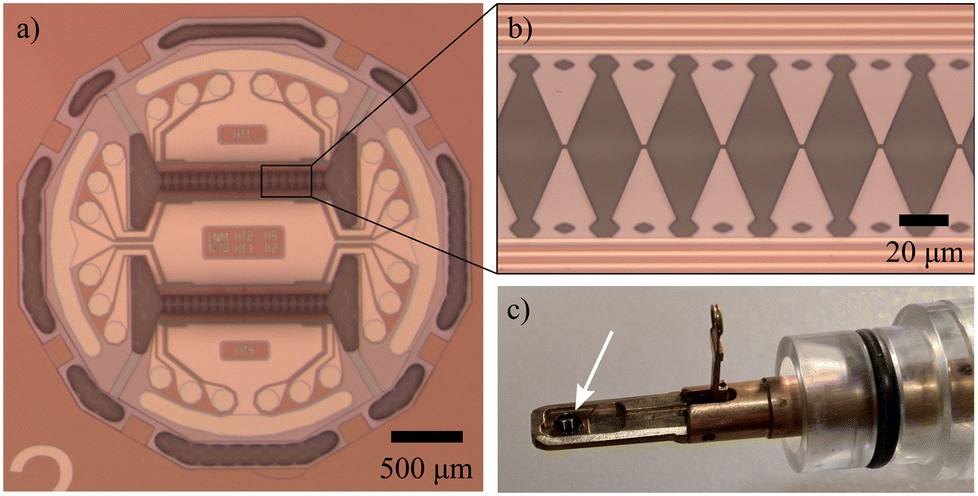 | ||
| Fig. 3 Optical images showing the fabricated device. (a) Overall view of the device after the last DRIE process performed at the backside, showing the partially opened outer rim. The shape of the 30 μm lateral suspended platforms at each side of the trenches are visible. (b) Detail of one suspended platform, including the microheaters. The compressed layer of buried silicon oxide is visible inside the trench areas. (c) Image of one microdevice on a TEM sample holder. The device is placed face down such that the focal plane is close to that expected for a standard TEM grid. | ||
Prior to the deposition of the Au catalyst nanoparticles used as NW seeds, a second wet HF etch is required to remove the protective SiO2 passivation layer over all metal pads. This etching also removes the remaining buried SiO2 layer, ensuring the thermal insulation of both sides of the trench. The distances between the cantilever pairs ranged from 2 to 20 μm in such a way that NWs with different lengths can be studied. Subsequently, following the procedure described in the experimental Section 2, epitaxial p-doped Si NWs were grown between the cantilever pairs. Fig. 4a and b show SEM images at different magnifications of an epitaxially integrated silicon NW over a pair of cantilevers.
 | ||
| Fig. 4 (a) and (b) SEM images at different magnifications of an integrated Si NW between a pair of cantilevers. The arrows illustrate the crystallographic orientation of the SOI. (c) and (d) TEM images of the same NW. The absence of substrate allows to resolve detail features of the NW morphology, such as the small Au nanoparticles (indicated with arrows) responsible of the secondary lateral growth at the surface of the NW. | ||
This platform hence offers several advantages over the commonly used suspended nitride micro-platforms.36 Firstly, the integrated growth of the NWs avoids the time-consuming task of transferring NWs from the growth substrate to the microdevice. In addition, the epitaxial growth of the NWs allows to drastically improve the widely known thermal contact issues.19 Yet, this comes at the price of losing the possibility of removing the electrical contact resistance between NW and bulk as the voltage collectors are in contact with the bulk. Finally, few microdevices featuring suspended nitride membranes have reported the compatibility with transmission experiments.37 Still, they require special TEM holders which are not commonly available. In contrast, the presented device can be used in standard TEM holders (Fig. 3c), making it compatible to almost every TEM.
TEM compatibility (Fig. 4c and d) allows to examine the NW structure in detail. High resolution can be achieved thanks to the absence of substrate under the sample. Notably, small Au particles could be resolved with unprecedented detail as illustrated in Fig. 4d. These small gold nano-particles are spilled from the main eutectic droplet during the NW growth and – according to Gadea et al.21 – were responsible for the growth of the lateral surface protrusions of the NWs fabricated under these conditions. The results of Fig. 4d suggests that this is indeed the mechanism behind the high roughness exhibited by these NWs.
3.2. Thermoelectric characterization
The experimental configuration used to measure the Seebeck coefficient of the integrated wire is sketched in the electrical simulation of the device (Fig. 5a). One of the internal heaters – central top in this case (see Fig. 1a and 3a) – was biased with a current IHT, creating a temperature difference ΔT (under vacuum) across the trench, as depicted in the inset of Fig. 5b. A comprehensive design of the heater area distribution – shifted towards the two sides of the trench – ensured a constant temperature across all cantilevers within a 2.2% precision. During the Seebeck experiment, the ΔT was incrementally increased up to 6 K, reached with 52 mW of dissipated power (4 mA), producing up to 2.1 ± 0.2 mV of thermovoltage (Fig. 5b). The Seebeck coefficient can be then extracted from the slope of the curve, yielding a value of 350.0 ± 5.6 μV K−1. | ||
| Fig. 5 (a) Schematic of the electrical simulation of the device during a Seebeck measurement. Blue-to-red color-map scales the voltage drop VHT across the central heater, whereas the green-to-yellow scale represents the induced voltages VTest at the collectors metal tracks (plotted in orange in Fig. 1a). A current IHT is supplied to the central heater to create the thermal gradient (see inset in b). This ΔT induces a voltage VW between the electrical collectors at both sides of the trenches. An oppositely polarized voltage is unavoidably built up across the central heater bulk, represented by VB. (b) Variation in VW as a function of the sustained ΔT at 400 K. The slope of the curve is the Seebeck coefficient. | ||
Notably, the thermovoltage was acquired between the two voltage collectors (VW in Fig. 5a), which remain insulated over the Si3N4 layer except for the area immediately in contact with the cantilevers. This prevents an underestimation of the NW response arising from a negative voltage artefact (denoted as VB in the sketch) generated by the opposite gradient built up in the doped SOI of the heated platform.
Fig. 6a illustrates how the V collectors allow to perform 4-probe measurements on the NWs avoiding the additional sheet resistance of the device Si layer. Fig. 6b shows the measured I–V curve at 400 K, while the corresponding NW resistance RNW as a function of the Joule dissipated power is depicted in Fig. 6c. A linear dependence with the applied power can be observed, matching the expected behaviour of a self-heating wire with a degenerated (metallic) behaviour, i.e. with a roughly constant positive TCR.26,38 The measured NW featured a geometric mean diameter of 102.0 ± 0.5 nm and a total length of 13.5 μm. Thus, the NW electrical conductivity σ is estimated at 180.3 ± 1.0 S cm−1 and hence the power factor yields 2.21 ± 0.06 mW K−2 m−1.
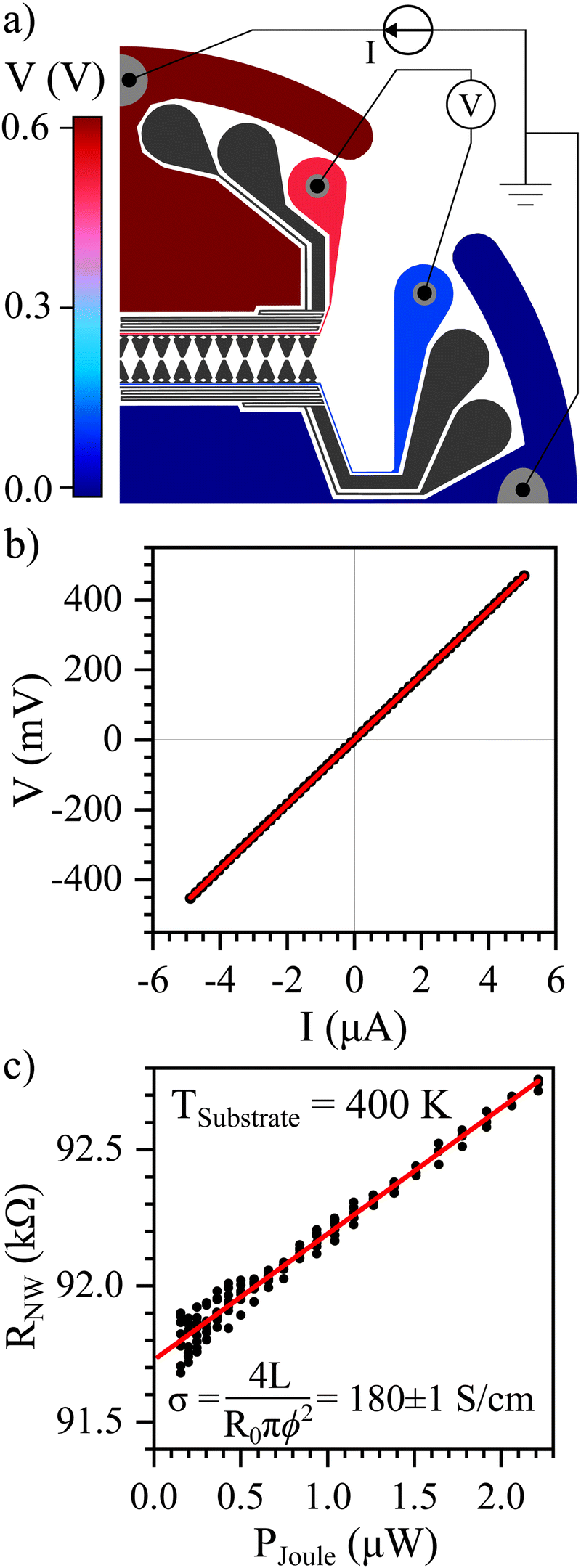 | ||
| Fig. 6 (a) Schematic of the electric simulation of the device during an I–V test on the NW. A 4-point measurement is carried out using the I and V collectors simultaneously to avoid the effect of the device's p-doped sheet resistance on both sides. (b) Measured I–V curve at 400 K. (c) Corresponding PJoule–R curve, used to compute R(P = 0). | ||
The thermal conductivity κ of the NW is usually the most challenging property to accurately measure, especially when dealing with integrated structures.21 With micro-Raman thermometry, the shift in the Stokes peak position induced by temperature changes (∂ω0/∂T) can be calibrated (Fig. S2, ESI†) in order to measure the local temperature along the NW.39 In this work, a calibrated value of ∂ω0/∂T was estimated to be 0.0194 ± 0.0006 cm−1 K−1 (inset of Fig. S2a, ESI†), being in relatively good agreement with literature data (0.022 ± 0.001 cm−1 K−1), where no significant differences were observed compared to bulk silicon.40,41 This difference might be caused by the NW's thermal expansion being slightly hindered by the fixed side walls, compressing the NW as it tries to expand and therefore avoiding the Raman peak to shift the same way as the freestanding NWs can do.42
Fig. 7a shows the obtained Raman shifts with respect to the reference (unheated) spectrum at each position for the case of TSubstrate = 300 K for two different applied Joule powers, i.e. with the current bias self-heating the NW. Fig. 7b illustrates the optical images of the relative laser position y with respect to the NW longitudinal axis. During the experiment the laser power was kept to 3 μW, low enough to avoid noticeable laser heating but still sufficient to resolve the signal (see inset of Fig. S2b, ESI†). The right axis depicts the correspondence with the temperature rise using the calibrated ∂ω0/∂T. A well-defined parabolic profile is observed for both applied Joule powers, being the maximum temperature directly proportional to the dissipated power. This is indeed the expected temperature profile of a homogeneously self-heated wire (under vacuum conditions) as it was described by Völklein et al.:43
 | (1) |
 .43 In the particular case depicted in Fig. 7a, this corresponds to average NW temperatures of 353 and 398 K for the low and high power cases, respectively. Fig. 7c illustrates the temperature dependence of κ. As it can be noticed, a linear trend is found when κ is plotted as a function of the average
  . Results match a purely electrical self-heating experiment depicted as black circles in Fig. 7c. Details of this standard experimental approach can be found elsewhere.26 In addition, the magnitude of κ can be reasonably modelled (solid line in Fig. 7c) by considering the phonon-boundary scattering proposed by Yang et al.44 This approach assumes a surface scattering rate beyond the fully diffusive Casimir limit, where phonons are trapped in multiple reflections at the protuberances of the NW surface (see Fig. 4d). However, experimental data show a higher temperature dependence with respect to the model, pointing to a possible underestimation of the Umklapp scattering processes together with an overestimation of the boundary scattering in the latter.
 | ||
| Fig. 7 (a) Raman peak shifts and corresponding temperature rise produced by two Joule heating powers of 10.5 μW and 15 μW (blue and red, respectively) measured along the NW axis. The solid line represents the fit of the data using eqn (1) and the shaded area the confidence interval (95%). (b) Sequence of optical microscope images showing the laser position along the NW. The central point (5th image) was used during the power tests (Fig. S2, ESI†) as it is the most sensitive position to heating. (c) Resulting thermal conductivity values as a function of the NW average temperature. Black circles show the obtained results using the self-heating method.26 The inset shows the calculated laser absorption coefficient using eqn (3). | ||
Moreover, it is remarkable to observe the absence of a sharp temperature step between the nanowire thermal profile and the bulk temperature. This constitutes direct proof of the negligible thermal contact resistance between NW and bulk as a consequence of the epitaxial growth of the NWs. This result agrees with the estimations of Gadea et al.21 using the transmission line method and our independent verification using Scanning Thermal Microscope experiments (SthM).45
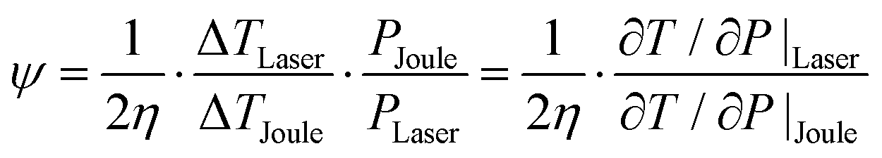
It is also worth noticing that no error in the measurement of κ is derived from the estimation of the laser power absorption coefficient ψ – a very challenging parameter to measure experimentally –,17 as the heating is done purely electrically. Indeed, ψ can be here estimated by comparing the ΔT profile expected when using electrical heating (eqn (1)) with the behaviour when using laser heating as a (quasi) punctual heat source as proposed by Soini et al.:27
 | (2) |
 | (3) |
Table 1 summarizes the obtained results for the studied nanowire. σ and S values measured are both consistent with a NW with doping concentration in the range of 1.5 × 10¹⁹ – 3.5 × 1019 cm−3,26 which was the level targeted with the diborane partial pressure used during the growth of the NWs (see Section 2). κ obtained is consistent between the two techniques used in this work, and the trend with temperature is negative, as expected from the increasing prevalence of Umklapp scattering in NWs of this diameter.13 The obtained absolute values are comparable to what is expected for a very rough silicon nanowire of this diameter (∼27 W Km−1).47,48 Overall, the resulting figure of merit for the NW at a typical thermoelectric operation temperature of 400 K is 0.036 ± 0.002, which is also consistent with previously reported values.21
| L (μm) | ϕ (nm) | σ (S cm−1) | S (μV K−1) | k (W mK−1) | zT (—) |
|---|---|---|---|---|---|
| 13 | 102.0 ± 0.5 | 180.0 ± 1.0 | 350.0 ± 5.6 | 24.3 ± 1.7 | 0.036 ± 0.002 |
Overall, this device will ease the optimization of nanowires for thermoelectric and optoelectronic applications, enabling their complete characterization within a single device. In particular, it will be especially interesting for the study of porous silicon nanowires,49–51 where proper characterization of the porosity typically requires high-resolution TEM. Additionally, structural characterization in synchrotron X-ray sources typically works in transmission mode.52 Hence, the absence of supporting substrate is particularly useful in this case as well. This device is also appealing for its use in the study of nanowires with ion-induced defects for the enhancement of phonon scattering.53,54 In all these possible measurements, in situ tests would be straightforwardly implemented similarly to the combined electro-opitcal measurements described in Fig. 7b. This can be particularly interesting for SthM experiments with simultaneous electrical and/or thermal excitation.45 This constitutes a further degree of freedom when planning these experiments.
4. Conclusions
This work presents the complete morphological, structural, and thermoelectric characterization of the selfsame individual epitaxially integrated nanowire. This study is enabled by the use of a unique and versatile multi-purpose test microdevice. Such device features an architecture without substrate underneath the sample, enabling transmission experiments for detailed morphological characterization, including TEM. The selfsame nanowire can then be electrically and thermally characterized, obtaining the whole set of properties from the same sample. Additionally, the chip can be fabricated in any crystallographic direction, thus enabling its potential use for other nanowire materials. Subsequently, the complete characterization of a fully epitaxially integrated rough Si nanowire using SEM, TEM, electrical and Raman techniques was carried out. Remarkably, no thermal contact resistance was observed after resolving the temperature profile along the nanowire, confirming our previous independent experiments. In addition, the optical absorption coefficient of the nanowires was estimated by combining Joule and laser heating experiments. Overall, this device will ease the optimization of nanowires for thermoelectric and optoelectronic applications, enabling their complete characterization within a single device. This constitutes a further degree of freedom when planning these experiments.Author contributions
J. M. S. G.: conceptualization, investigation, validation, data curation, formal analysis, visualization, software, writing – original draft; Y. K.: investigation, methods, writing – review and editing; S. T.: investigation, data curation, writing – original draft; N. A.: conceptualization, methods; N. F.: investigation; M. S.: investigation, methods, resources, writing – review and editing; L. F.: resources, funding acquisition, writing – review and editing; A. M.: resources, funding acquisition, writing – review and editing; A. T.: resources, funding acquisition, writing – review and editing; I. Z.: conceptualization, funding acquisition, writing – review and editing.Conflicts of interest
There are no conflicts to declare.Acknowledgements
This investigation has been supported by the Spanish Ministry of Education through the FPU grant FPU18/01494, and by the University and Research Secretary of the Business and Knowledge Department of the Generalitat de Catalunya in the project FEM-IoT (001-P-001662). This work acknowledges the financial support from the Agencia de Gestió d’Ajuts Universitaris i de Recerca (AGAUR) of the Generalitat de Catalunya (2021 SGR 00497). This research has also been supported by the Spanish National Research Agency (AEI) through the project THERMOLOGICS (AEI/FEDER, EU, PID2019-110142RB-C21). This research has used the Spanish ICTS Network MICRONANOFABS, partially funded by FEDER funds through MINATEC-PLUS-2 project (FICTS2019-02-40). This project has received funding from the Swiss National Science Foundation grant (Grant No. 189924) HYDRONICS and from the European Research Council (ERC) under the European Union's Horizon 2020 research and innovation program (Grant Agreement 756365).References
- C. Jia, Z. Lin, Y. Huang and X. Duan, Nanowire Electronics: From Nanoscale to Macroscale, Chem. Rev., 2019, 119, 9074–9135 CrossRef CAS PubMed.
- Y. Zhang, J. Wu, M. Aagesen and H. Liu, III–V nanowires and nanowire optoelectronic devices, J. Phys. D: Appl. Phys., 2015, 48, 463001 CrossRef.
- L. N. Quan, J. Kang, C.-Z. Ning and P. Yang, Nanowires for Photonics, Chem. Rev., 2019, 119, 9153–9169 CrossRef CAS PubMed.
- M. Y. Swinkels and I. Zardo, Nanowires for heat conversion, J. Phys. D: Appl. Phys., 2018, 51, 353001 CrossRef.
- N. I. Goktas, P. Wilson, A. Ghukasyan, D. Wagner, S. McNamee and R. R. LaPierre, Nanowires for energy: A review, Appl. Phys. Rev., 2018, 5, 041305 Search PubMed.
- J. M. Sojo Gordillo, A. Morata, C. D. Sierra, M. Salleras, L. Fonseca and A. Tarancon, Recent advances in silicon-based nanostructures for thermoelectric applications, APL Mater., 2023, 11, 040702 CrossRef.
- E. Hittinger and P. Jaramillo, Internet of things: Energy boon or bane?, Science, 2019, 364, 326–328 CrossRef CAS PubMed.
- A. Tarancon, Powering the IoT revolution with heat, Nat. Electron., 2019, 2, 270–271 CrossRef.
- O. H. Ando Junior, A. L. Maran and N. C. Henao, A review of the development and applications of thermoelectric microgenerators for energy harvesting, Renewable Sustainable Energy Rev., 2018, 91, 376–393 CrossRef.
- Q. Zhang, K. Deng, L. Wilkens, H. Reith and K. Nielsch, Micro-thermoelectric devices, Nat. Electron., 2022, 5, 333–347 CrossRef.
- M. Haras and T. Skotnicki, Thermoelectricity for IoT – a review, Nano Energy, 2018, 54, 461–476 CrossRef CAS.
- P. Kim, L. Shi, A. Majumdar and P. L. McEuen, Thermal Transport Measurements of Individual Multiwalled Nanotubes, Phys. Rev. Lett., 2001, 87, 215502 CrossRef CAS PubMed.
- D. Li, Y. Wu, P. Kim, L. Shi, P. Yang and A. Majumdar, Thermal conductivity of individual silicon nanowires, Appl. Phys. Lett., 2003, 83, 2934–2936 CrossRef CAS.
- A. I. Hochbaum, R. Chen, R. D. Delgado, W. Liang, E. C. Garnett, M. Najarian, A. Majumdar and P. Yang, Enhanced thermoelectric performance of rough silicon nanowires, Nature, 2008, 451, 163–167 CrossRef CAS PubMed.
- P. Ferrando-Villalba, A. F. Lopeandia, L. Abad, J. Llobet, M. Molina-Ruiz, G. Garcia, M. Gerboles, F. X. Alvarez, A. R. Goñi, F. J. Munoz-Pascual and J. Rodriguez-Viejo, In-plane thermal conductivity of sub-20 nm thick suspended mono-crystalline Si layers, Nanotechnology, 2014, 25, 185402 CrossRef CAS PubMed.
- S. Shin, M. Elzouka, R. Prasher and R. Chen, Far-field coherent thermal emission from polaritonic resonance in individual anisotropic nanoribbons, Nat. Commun., 2019, 10, 1–11 CrossRef PubMed.
- M. Y. Swinkels, A. Campo, D. Vakulov, W. Kim, L. Gagliano, S. E. Steinvall, H. Detz, M. De Luca, A. Lugstein, E. Bakkers, I. Fontcuberta, A. Morral and I. Zardo, Measuring the Optical Absorption of Single Nanowires, Phys. Rev. Appl., 2020, 14(2), 024045 CrossRef CAS.
- D. Vakulov, et al., Ballistic Phonons in Ultrathin Nanowires, Nano Lett., 2020, 20, 2703–2709 CrossRef CAS PubMed.
- M. Y. Swinkels, M. R. Van Delft, D. S. Oliveira, A. Cavalli, I. Zardo, R. W. Van Der Heijden and E. Bakkers, Diameter dependence of the thermal conductivity of InAs nanowires, Nanotechnology, 2015, 26, 385401 CrossRef CAS PubMed.
- S. Yazji, M. Y. Swinkels, M. De Luca, E. A. Hoffmann, D. Ercolani, S. Roddaro, G. Abstreiter, L. Sorba, E. P. A. M. Bakkers and I. Zardo, Assessing the thermoelectric properties of single InSb nanowires: the role of thermal contact resistance, Semicond. Sci. Technol., 2016, 31, 064001 CrossRef.
- G. Gadea, J. M. Sojo Gordillo, M. Pacios Pujado, M. Salleras, L. Fonseca, A. Morata and A. Tarancon Rubio, Enhanced thermoelectric figure of merit of individual Si nanowires with ultralow contact resistances, Nano Energy, 2020, 67, 104191 CrossRef.
- J. M. Sojo-Gordillo, C. D. Sierra, G. Gadea Diez, J. Segura-Ruiz, V. Bonino, M. Nunez Eroles, J. C. Gonzalez-Rosillo, D. Estrada-Wiese, M. Salleras, L. Fonseca, A. Morata and A. Tarancon, Superior Thermoelectric Performance of SiGe Nanowires Epitaxially Integrated into Thermal Micro-Harvesters, Small, 2023, 19, 2206399 CrossRef CAS PubMed.
- G. Gadea, A. Morata, J. D. Santos, D. Davila, C. Calaza, M. Salleras, L. Fonseca and A. Tarancon, Towards a full integration of vertically aligned silicon nanowires in MEMS using silane as a precursor, Nanotechnology, 2015, 26, 195302 CrossRef CAS PubMed.
- A. I. Hochbaum, R. Fan, R. He and P. Yang, Controlled growth of Si nanowire arrays for device integration, Nano Lett., 2005, 5, 457–460 CrossRef CAS PubMed.
- G. Gadea, Integration of Si/Si-Ge nanostructures in micro-thermoelectric generators, PhD thesis, Universidad de Barcelona, 2017.
- J. M. Sojo-Gordillo, D. Estrada-Wiese, C. Duque-Sierra, G. Gadea Diez, M. Salleras, L. Fonseca, A. Morata and A. Tarancon, Tuning the thermoelectric properties of boron-doped silicon nanowires integrated into a micro-harvester, Adv. Mater. Technol., 2022, 7(10), 2101715 CrossRef CAS.
- M. Soini, I. Zardo, E. Uccelli, S. Funk, G. Koblmuller, I. Fontcuberta, A. Morral and G. Abstreiter, Thermal conductivity of GaAs nanowires studied by micro-Raman spectroscopy combined with laser heating, Appl. Phys. Lett., 2010, 97, 16–18 CrossRef.
- S. Yazji, E. A. Hoffman, D. Ercolani, F. Rossella, A. Pitanti, A. Cavalli, S. Roddaro, G. Abstreiter, L. Sorba and I. Zardo, Complete thermoelectric benchmarking of individual InSb nanowires using combined micro-Raman and electric transport analysis, Nano Res., 2015, 8, 4048–4060 CrossRef CAS.
- F. W. DelRio, R. F. Cook and B. L. Boyce, Fracture strength of micro- and nano-scale silicon components, Appl. Phys. Rev., 2015, 2, 021303 Search PubMed.
- D. Estrada-Wiese, J.-M. Sojo, M. Salleras, J. Santander, M. Fernandez-Regulez, I. Martin-Fernandez, A. Morata, L. Fonseca and A. Tarancon, Harvesting performance of a planar thermoelectric microgenerator with a compact design, 2021, IEEE 20th International Conference on Micro and Nanotechnology for Power Generation and Energy Conversion Applications (PowerMEMS), 2021, pp. 108–111.
- V. Schmidt, S. Senz and U. Gosele, Diameter-dependent growth direction of epitaxial silicon nanowires, Nano Lett., 2005, 5, 931–935 CrossRef CAS PubMed.
- C. X. Wang, M. Hirano and H. Hosono, Origin of Diameter-Dependent Growth Direction of Silicon Nanowires, Nano Lett., 2006, 6, 1552–1555 CrossRef CAS PubMed.
- A. L. Roest, M. A. Verheijen, O. Wunnicke, S. Serafin, H. Wondergem and E. P. A. M. Bakkers, Position-controlled epitaxial III - V nanowires on silicon, Nanotechnology, 2006, 271–275 CrossRef.
- H. Zeng, X. Yu, H. A. Fonseka, G. Boras, P. Jurczak, T. Wang, A. M. Sanchez and H. Liu, Preferred growth direction of III–V nanowires on differently oriented Si substrates, Nanotechnology, 2020, 31, 475708 CrossRef CAS PubMed.
- C. Y. Yang, S. M. Yang, Y. Y. Chen and K. C. Lu, Fabrication and Physical Properties of Single-Crystalline Beta-FeSi2 Nanowires, Nanoscale Res. Lett., 2020, 15(1), 197 CrossRef CAS PubMed.
- L. Shi, D. Li, C. Yu, W. Jang, D. Kim, Z. Yao, P. Kim and A. Majumdar, Measuring Thermal and Thermoelectric Properties of One-Dimensional Nanostructures Using a Microfabricated Device, J. Heat Transfer, 2003, 125, 881 CrossRef CAS.
- G. de Vito, D. M. Koch, G. Raciti, J. M. Sojo-Gordillo, A. Nigro, R. Swami, Y. Kaur, M. Y. Swinkels, W. Huang, T. Paul, M. Calame and I. Zardo, Suspended micro thermometer for anisotropic thermal transport measurements, Int. J. Heat Mass Transfer, 2024, 224, 125302 CrossRef.
- G. Pennelli, E. DImaggio and M. MacUcci, Note: Improvement of the 3ω thermal conductivity measurement technique for its application at the nanoscale, Rev. Sci. Instrum., 2018, 89, 16102–16105 CrossRef PubMed.
- G. S. Doerk, C. Carraro and R. Maboudian, Single Nanowire Thermal Conductivity Measurements by Raman Thermography, ACS Nano, 2010, 4, 4908–4914 CrossRef CAS PubMed.
- T. R. Hart, R. L. Aggarwal and B. Lax, Temperature dependence of Raman scattering in silicon, Phys. Rev. B: Solid State, 1970, 1, 638–642 CrossRef.
- G. S. Doerk, C. Carraro and R. Maboudian, Temperature dependence of Raman spectra for individual silicon nanowires, Phys. Rev. B: Condens. Matter Mater. Phys., 2009, 80, 1–4 CrossRef.
- K. F. Murphy, B. Piccione, M. B. Zanjani, J. R. Lukes and D. S. Gianola, Strain- and defectmediated thermal conductivity in silicon nanowires, Nano Lett., 2014, 14, 3785–3792 CrossRef CAS PubMed.
- F. Volklein, H. Reith, T. W. Cornelius, M. Rauber and R. Neumann, The experimental investigation of thermal conductivity and the Wiedemann-Franz law for single metallic nanowires, Nanotechnology, 2009, 20, 325706 CrossRef CAS PubMed.
- H.-Y. Yang, Y.-L. Chen, W.-X. Zhou, G.-F. Xie and N. Xu, Ultra-low thermal conductivity of roughened silicon nanowires: Role of phonon-surface bond order imperfection scattering, Chin. Phys. B, 2020, 0–14 Search PubMed.
- J. M. Sojo-Gordillo, G. Gadea Diez, D. Renahy, M. Salleras, C. Duque-Sierra, P. Vincent, L. Fonseca, P.-O. Chapuis, A. Morata, S. Gomès and A. Tarancón, Local heat dissipation and elasticity of suspended silicon nanowires revealed by dual scanning electron and thermal microscopies, Small, 2023, 2305831 Search PubMed.
- J. Anaya, A. Torres, A. Martin-Martin, J. Souto, J. Jimenez, A. Rodriguez and T. Rodriguez, Study of the temperature distribution in Si nanowires under microscopic laser beam excitation, Appl. Phys. A: Mater. Sci. Process., 2013, 113, 167–176 CrossRef CAS.
- L. N. Maurer, Z. Aksamija, E. B. Ramayya, A. H. Davoody and I. Knezevic, Universal features of phonon transport in nanowires with correlated surface roughness, Appl. Phys. Lett., 2015, 106, 133108 CrossRef.
- J. Lim, K. Hippalgaonkar, S. C. Andrews, A. Majumdar and P. Yang, Quantifying surface roughness effects on phonon transport in silicon nanowires, Nano Lett., 2012, 12, 2475–2482 CrossRef CAS PubMed.
- K. Valalaki, P. Benech and A. Galiouna Nassiopoulou, High Seebeck Coefficient of Porous Silicon: Study of the Porosity Dependence, Nanoscale Res. Lett., 2016, 11(1), 201 CrossRef PubMed.
- P. Ferrando-Villalba, L. D’Ortenzi, G. G. Dalkiranis, E. Cara, A. F. Lopeandia, L. Abad, R. Rurali, X. Cartoixa, N. De Leo, Z. Saghi, M. Jacob, N. Gambacorti, L. Boarino and J. Rodriguez-Viejo, Impact of pore anisotropy on the thermal conductivity of porous Si nanowires, Sci. Rep., 2018, 8, 12796 CrossRef CAS PubMed.
- L. Yang, D. Huh, R. Ning, V. Rapp, Y. Zeng, Y. Liu, S. Ju, Y. Tao, Y. Jiang, J. Beak, J. Leem, S. Kaur, H. Lee, X. Zheng and R. S. Prasher, High thermoelectric figure of merit of porous Si nanowires from 300 to 700 K, Nat. Commun., 2021, 12, 3926 CrossRef CAS PubMed.
- J. Segura-Ruiz, G. Martinez-Criado, C. Denker, J. Malindretos and A. Rizzi, Phase Separation in Single In x Ga 1- x N Nanowires Revealed through a Hard X-ray Synchrotron Nanoprobe, Nano Lett., 2014, 14, 1300–1305 CrossRef CAS PubMed.
- N. S. Bennett, N. M. Wight, S. R. Popuri and J. W. G. Bos, Efficient thermoelectric performance in silicon nano-films by vacancy-engineering, Nano Energy, 2015, 16, 350–356 CrossRef CAS.
- N. S. Bennett, D. Byrne, A. Cowley and N. Neophytou, Dislocation loops as a mechanism for thermoelectric power factor enhancement in silicon nano-layers, Appl. Phys. Lett., 2016, 109(17), 173905 CrossRef.
Footnote |
| † Electronic supplementary information (ESI) available: Additional referenced figures and tables as well as details of the calibration process. See DOI: https://doi.org/10.1039/d4nh00114a |
| This journal is © The Royal Society of Chemistry 2024 |