
Strongly polarized color conversion of isotropic colloidal quantum dots coupled to fano resonances†
Kivanc
Gungor
a,
Onur
Erdem
a,
Burak
Guzelturk
 a,
Emre
Unal
a,
Shinae
Jun
b,
Eunjoo
Jang
c and
Hilmi Volkan
Demir
*ad
a,
Emre
Unal
a,
Shinae
Jun
b,
Eunjoo
Jang
c and
Hilmi Volkan
Demir
*ad
aDepartment of Electrical and Electronics Engineering, Department of Physics, UNAM--Institute of Materials Science and Nanotechnology and the National Nanotechnology Research Center, Bilkent University, Ankara, 06800, Turkey. E-mail: volkan@stanfordalumni.org
bInorganic Material Laboratory, Material Research Center, Samsung Advanced Institute of Technology, Samsung Electronics Co., 130 Samsung-ro, Yeongtong-gu, Suwon-si, Gyeonggi-do 443-803, South Korea
cSKKU Advanced Institute of Nanotechnology (SAINT), Sungkyunkwan University (SKKU), 2066 Seobu-ro, Jangan-gu, Suwon, Gyeonggi-do 16419, Republic of Korea
dLuminous! Center of Excellence for Semiconductor Lighting and Displays, School of Electrical and Electronic Engineering, School of Physical and Mathematical Sciences, and School of Materials Science and Engineering, Nanyang Technological University, Singapore 639798, Singapore
First published on 24th July 2024
Abstract
Colloidal quantum dots (QDs) offer high color purity essential to high-quality liquid crystal displays (LCDs), which enables unprecedented levels of color enrichment in LCD-TVs today. However, for LCDs requiring polarized backplane illumination in operation, highly polarized light generation using inherently isotropic QDs remains a fundamental challenge. Here, we show strongly polarized color conversion of isotropic QDs coupled to Fano resonances of v-grooved surfaces compatible with surface-normal LED illumination for next-generation QD-TVs. This architecture overcomes the critically oblique excitation of surface plasmon coupled emission by using v-shapes imprinted on the backlight unit (BLU). With isotropic QDs coated on the proposed v-BLU surface, we experimentally measured a far-field polarization contrast ratio of ∼10. Full electromagnetic solution shows Fano line-shape transmission in transverse magnetic polarization allowing for high transmission as an indication for forward-scattering configuration. Of these QDs coupled to the surface plasmon-polariton modes, we observed strong modifications in their emission kinetics revealed by time-resolved photoluminescence spectroscopy and via dipole orientations identified by back focal plane imaging. This collection of findings indicates conclusively that these isotropic QDs are forced to radiate in a linearly polarized state from the patterned planar surface under surface-normal excitation. For next-generation QD-TVs, the proposed polarized color-converting isotropic QDs on such v-BLUs can be deployed in bendable electronic displays.
New conceptsSemiconductor nanocrystals are highly promising for use in advanced photonic applications. Color conversion in LCDs is the first successful large-scale commercial application of nanocrystals. However, conventional device architectures fully exploit the potential of nanocrystals. LCDs require linearly-polarized light coming from the backplane. The polarization state of this polarized light can be controlled by LC cells. Therefore, a rear polarizer at the back clips the undesired polarization state if the backlight illumination is unpolarized. This way each LC cell provides switching capability for each pixel. The process of eliminating the undesired polarization of the randomly polarized back-illumination naturally wastes half of the generated light. Here we proposed and demonstrated innovative photon management enabled by isotropic colloidal semiconductor nanocrystals coupled to Fano resonances for polarized color conversion. We also studied the plasmonic interaction mechanisms that modify the density of optical states. Here, the strong dipole orientation dependence of surface plasmon coupled emission is utilized in tailored grooves defined into a v-shaped backlight unit structure. Consequently, forward scattering of Fano resonance effectively allows for polarized light generation that can freely radiate into the farfield. We experimentally achieved a high contrast ratio reaching 10, measured in the farfield similar to LCD operation. |
Liquid crystal displays (LCD) revolutionized the display market. Colloidal semiconductor quantum dots (QDs) possess spectrally tunable narrow-band emission, which is important for color purity in LCDs, accompanied with broad-band absorption making optical excitation possible at short wavelengths.1 Decades of research resulted in high stability,2 near-unity efficiency3,4 and spectrally engineered pure color-enriching QDs.4,5 With careful spatial placement of QDs, e.g., via inkjet printing, transfer printing6 and lithographic techniques,7 QDs offer pixelated color conversion. Conventionally, rare-earth based phosphors are used for color-conversion; however, there have been major supply concerns for rare-earth elements.8 In contrast, wide availability and vast material choices for solution-processed QDs make them excellent color-converting alternatives. The QD-based backlights in the LCDs can favorably enhance the color gamut beyond the performance limits of phosphor-based backlights.9–11 Considering the listed advantages, QDs have attracted great interest from the display industry and QD-enhanced LCDs dominate the display market today.12–17
In advanced LCDs, a back-illuminating light source, typically containing blue light-emitting diodes – LEDs, is used to excite color-converting materials placed behind the liquid crystal cells (LCC). A rear polarizer is placed between the LCCs and the color conversion layer. LCCs change the polarization state of linearly polarized light passed through the rear polarizer, which clips the undesired polarization of emission from the color-converting material and unconverted portion of the blue back-light illumination. Another polarizer in the front-plane of the LCCs selectively passes only the light with the right polarization state, which can be addressed and changed by the individual LCCs. Finally, a color filter is used to create color selective pixels each defined by an LCC. During the display operation, each optical component (polarizers, color filters, color converting materials) induces an inherent loss and significantly reduces the efficiency of an LCD unit. Out of these, the rear polarizer results in a major loss of at least 50%, which is one of the limiting factors in the overall efficiency of LCDs. Therefore, there is a strong need for polarized backlight sources to address the overall efficiency problem of current LCDs. Today the LCDs based on the QD-backlights suffer from the randomly polarized light of isotropic QDs similar to phosphor-based LCDs that require utilization of rear polarizers. Here, to address this problem, we proposed and demonstrated strongly polarized color conversion of isotropic QD emitters coupled to Fano resonance of v-grooved surfaces. With the proposed structure, it is possible to make ultra-thin, bendable and uniform displays incorporated with any type of nanocrystal emitters.
Efforts to achieve polarized light generation from semiconductor nanocrystals mainly focused on their shape modification and emission control. Anisotropic nanocrystals inherently emit partially polarized light at a single particle level;18 however, in ensemble they require aligned immobilization on a surface making their use impractical at a large scale.19 Polarized emission of rod-in-rod nanocrystals in a stretched polymer film has been reported. This method is not flexible in terms of luminophore choices and makes use of mainly the anisotropy resulting from the absorption characteristics.20 In an alternative approach, metallic gratings can be used as a polarizing unit in conjunction with color-converting QDs for light generation. Nevertheless, there is a fundamental trade-off between the optical transmission and anisotropy values for the reported metallic grating structures.21–23 As another optical structure, photonic crystal cavities can be used for manipulating the optical density of states of the quantum emitters. Although photonic crystal cavities showed a high polarization contrast ratio, these efforts remained at a single particle level.24 Also, plasmonic coupling is a strong light interaction mechanism useful for optical density of states control over the quantum emitters. Gold nanorods were previously reported to be coated with emitters,25,26 however, they may require nanoparticle alignment on the surface. Plasmonic nanohole antennas27 and silver gratings28 coupled to QD emission suffer from low transmission values. PL decay modification using all-colloidal plasmonic cavities to achieve anisotropic emission has also been reported, but the oblique illumination requirement of these cavities prevent their use in display backplanes.29
In addition to the aforementioned structures, surface plasmon coupled emission (SPCE) is an inherently strong polarization dependent mechanism for various fluorescent molecules and quantum emitters.30,31 However, wide utilization of the SPCE mechanism in polarized light generation is limited due to light emission that occurs only at a specific angle in SPCE. In this work, we use the strong polarization dependence of the SPCE mechanism in a front-panel compatible configuration by using v-shaped grooves patterned on the surface. Strong coupling between surface plasmon-polariton (SPP) modes and isotropic QDs results in polarized emission from the planar surface under surface-normal excitation. As illustrated in Fig. 1, direct integration of isotropic QDs to front-panel displays makes polarized mode operation possible. Here, in operation, blue LED emission excites isotropic QDs deposited on the surface of a v-shaped backlight unit (v-BLU). The resulting polarized emission of QDs coupled to v-BLU passes through LCCs and then the front polarizer selectively passes the desired polarization state.
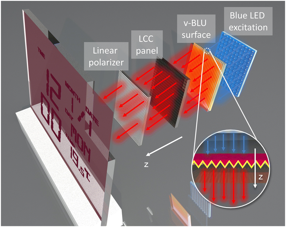 | ||
| Fig. 1 Proposed display architecture of the v-BLU surface coupled with an isotropic QD emitter. Randomly polarized blue LED in surface-normal configuration excites QDs on the v-BLU surface. The emitted light from the QDs integrated intimately with the v-BLU is strongly linearly polarized. The inset figure illustrates the excitation configuration of the proposed v-BLU structure. | ||
Our v-BLUs are fabricated using a silicon mold that is patterned with elongated v-shaped grooves. Previous efforts on surface patterning focused on the fabrication of metalenses,32,33 nanoantennas34,35 or optical waveguiding.36,37 While there are demonstrations of proof-of-concept display devices made of patterned QDs,38,39 these systems primarily produced unidirectional emission without changing the degree of polarization. Compared to the studies that report directional polarized emission by incorporating surface patterning,40 our work uses plasmonic enhancement of the desired polarization in addition to the suppression of the unwanted polarization component.
Results and discussions
The v-BLU surface is fabricated using a mold for the replication process. Several new replicates can be stripped off from the mold surface reducing the fabrication costs for commercial applications. Fabrication of the v-BLU is illustrated in Fig. 2a. The v-shape of the grooves is created by utilizing the crystallographic plane-selective etch rates of single crystal silicon wafer. We used several nanolithography techniques for mold fabrication including of electron beam lithography, dry- and wet-etching steps and a silanization process to reduce the surface energy of the mold.41–43 After the thermal deposition of thin plasmonic layers on mold, replicates were stripped off with the micrometer-thick support polymer layer. Cross-sectional scanning electron microscopy images of the mold (Fig. 2b) and replicate (Fig. 2c) show a high-quality replication process using the template stripping method. The CdSe/CdS/ZnS/CdSZnS core/multi shell QD spin-casted on the v-groove film replicates (25 mg mL−1 1000 rpm, 1 min) are synthesized using a previously reported recipe.4,44 These red-emitting QDs have an average size of 8.6 nm, capped with oleic acid (OA) ligands and dissolved in toluene.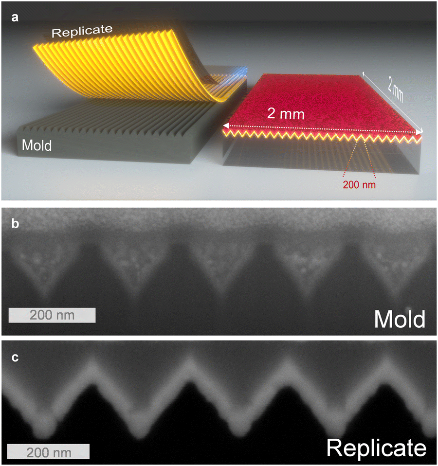 | ||
| Fig. 2 (a) Illustration of the developed fabrication method and final structure of the proposed v-BLU. After metal layer deposition, v-BLU together with the support layer polymer is stripped off from the silicon mold. (b) Cross-sectional scanning electron microscopy image of the fabricated mold structure. (c) Cross-sectional image of the replicated gold v-BLU with QDs. | ||
Optical transmission spectral characterization of v-BLU
Optical transmission spectra of gold v-BLU before and after the QD layer deposition are presented in Fig. 3a. Depending on the thickness of the QD layer, the plasmonic response of the structures is changing. Due to the effective refractive index increase, a redshift in the position of SPP resonance is expected.45 TE polarization is similar to plain gold film transmission since the impinging electromagnetic radiation will experience no surface feature in TE polarization. Fig. 3b shows the TM/TE transmission ratio of the gold structure before and after depositing QDs. For both thin and thick QD depositions, we obtain a TM/TE ratio of ∼5 at 620 nm wavelength, which is the PL emission peak wavelength of our red-emitting QDs. If the v-BLU design was only clipping a portion of the rejected polarization, both thin and thick deposition of QDs would provide similar polarization-dependent PL emission. The gray dashed line in Fig. 3b presents the flat gold film TM/TE ratio being unity and this unity TM/TE ratio shows that there is no inherent anisotropy originating from the measurement setup. To understand the polarization mechanism of the v-BLU, numerical simulation results of only the gold structure without QDs are given in Fig. 3c. The simulations for TM and TE polarizations agree well with the experimentally measured transmission.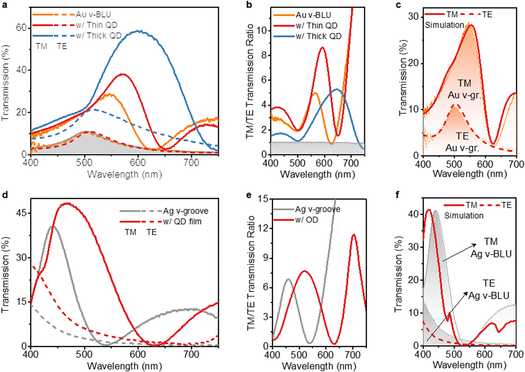 | ||
| Fig. 3 (a) Transmission spectra of gold v-BLUs with different red QD layer thicknesses. The thicker QD layer results in a redshifted and increased transmission response for TM polarization. TE polarization for thin QD layered structures is similar to the flat gold film transmission response plotted in the gray shaded curve. (b) The transmission TM/TE ratio for gold v-BLU shows an increased polarization level for structures with QDs. Around the red QD emission peak wavelength (620 nm), the TM/TE ratio is ∼5 for both structures. The gray shaded curve of the flat gold film TM/TE ratio is unity. (c) Experimental and simulated transmission spectra of gold v-BLU. (d) Transmission spectra of silver v-BLU before and after green QD layer deposition. The presence of the QD layer results in a redshifted and increased transmission response for TM mode similar to gold v-BLU. (e) The transmission TM/TE ratio for silver v-BLU shows an increased polarization level after QD deposition. Around the green QD emission peak wavelength (540 nm), the TM/TE ratio is ∼7. (f) Experimental and simulated transmission spectra of silver v-BLU. | ||
To further extend the polarization capabilities of v-BLU to the green region of the visible spectrum, a silver v-BLU was fabricated. Considering the surface plasmon resonance frequency, the silver v-BLU can be used for green QDs without further optimizing our mold structure to achieve polarized emission in the green region. We therefore fabricated additional v-BLU structures using the same mold and with silver as the plasmonic layer. Green-emitting CdSe/ZnS/CdZnS core/multi-shell QDs (d = 5.5 nm) capped with OA44 and dissolved in toluene were spin-casted (1000 rpm, 1 min) on top of silver. In Fig. 3d, silver v-BLU transmission before and after QD deposition is shown. Similar to gold v-BLU, we observed an increase and redshift in transmission after the QD deposition. At the green QD peak emission wavelength (540 nm), the silver v-BLU results in a TM/TE transmission ratio of ∼7 (Fig. 3e). The umerical simulation of transmission spectra is in agreement for the TM and TE polarizations with the experimental measurements as shown in Fig. 3f. Another observation is the similar transmission line-shapes of silver and gold v-BLU TM polarizations. This observation suggests that the transmission line-shape of TM polarization is characteristic to the v-BLU structure.
Fano line-shape of the transmission spectrum of v-BLU TM polarization
Before and after QD deposition, the transmission spectra of gold and silver v-BLUs follow a typical Fano resonance forward-scattering line-shape.46–50 In the forward-scattering Fano resonance, there should be an enhanced level of transmission for wavelengths shorter than the resonance wavelength and longer than the resonance wavelength, and transmission should decrease considerably. Impinging electromagnetic field intensities are mapped for the simulated gold v-BLU in Fig. 4. For the TE polarization, there is no significant change in the transmission regardless of the wavelength. In contrast, different wavelength points in the TM polarization transmission spectra show distinct intensity maps. Without QD deposition, the gold v-BLU exhibits a resonance wavelength around 593 nm for the TM polarization. Field maps show increasing transmission for a 550 nm wavelength, as an indication of forward-scattering. At 593 nm, the transmission spectrum changes its shape and wavelengths longer than the resonance wavelength features a reduced transmission. This reduced transmission is clearly observed in the intensity maps for longer wavelengths as shown for 625 nm. Furthermore, there is a stark contrast between field intensity magnitudes for the TM and TE polarizations between the v-grooves where QDs are deposited. In addition to transmission selectivity for different polarizations, an increased electric field intensity enhances the optical mode density for QDs in the TM polarization Ex direction. Enhanced optical modes in the x-direction indicate polarized emission parallel to the groove direction.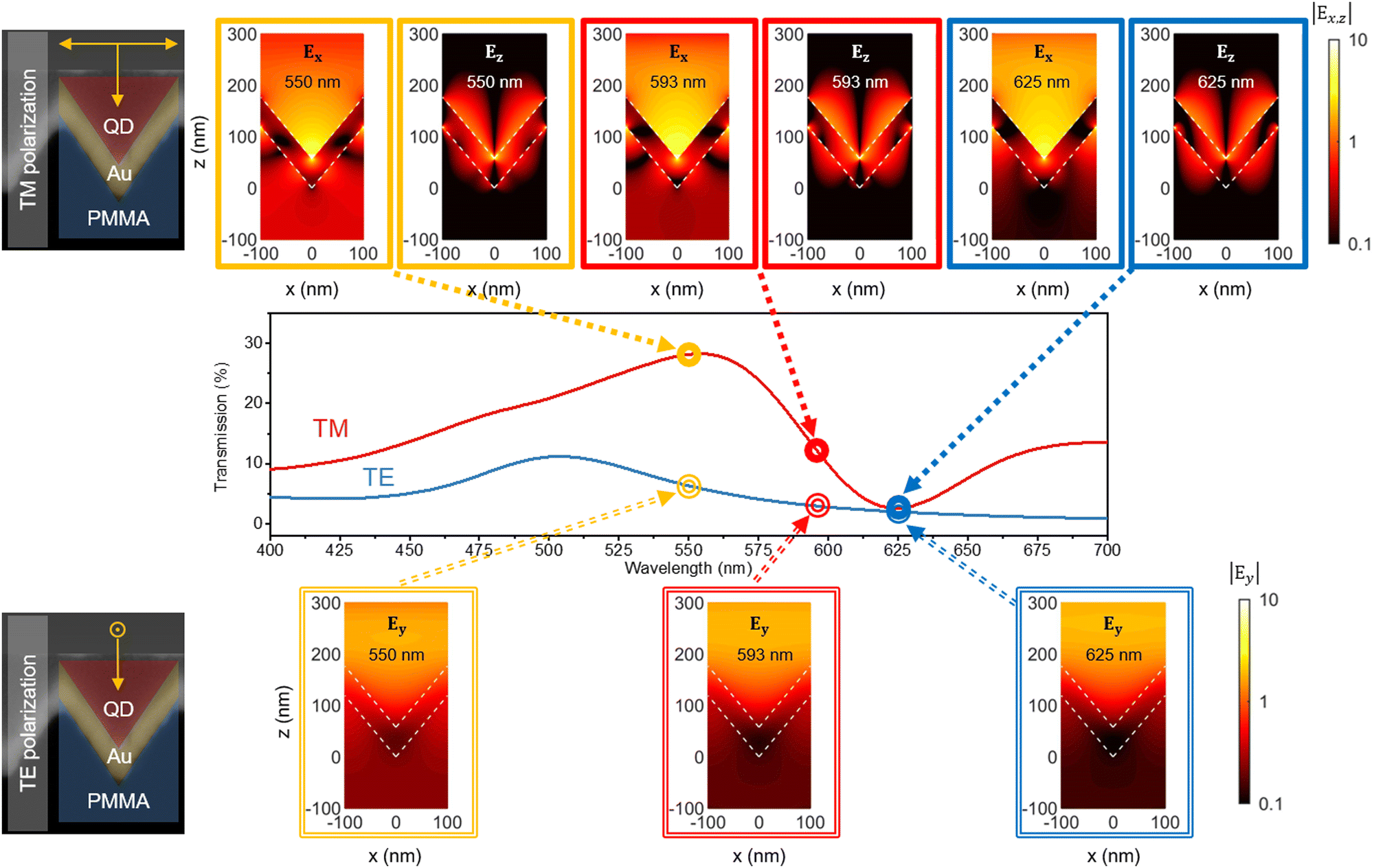 | ||
| Fig. 4 FDTD modeling of gold v-BLU without a QD layer. TM and TE polarization orientations are illustrated on the left and, when deposited on v-BLU, the position of QDs are shown in red color. The TM polarization transmission response resembles a Fano type resonance line-shape and the observed higher transmission for shorter wavelengths is an indication for forward-scattering configuration. Electric field intensity maps are showing increased transmission for the shorter wavelengths than the resonance wavelength of 593 nm. Also, the gap where QDs are deposited shows an increased electric field intensity, which increases the optical density of states for QDs. TE polarization shows no sign of strong resonance behavior and both transmission and electric field density values are significantly lower than TM polarization. | ||
Steady-state polarized emission of isotropic QDs on v-BLU in the far-field
After analyzing the transmission polarization response of v-BLUs, we measured their steady-state far-field photoluminescence under different polarizations. The measurement setup is similar to LCD operation as illustrated in Fig. 5a. We used a 400 nm linearly-polarized laser source to excite v-BLUs with an angle of 45° to groove directions ensuring the excitation of both TM and TE polarization states equally. The laser excites the QDs at normal incidence and PL from QDs is collected after rotating the analyzer to different angles. Absorption and PL of green-emitting (λPL = 540 nm) and red-emitting (λPL = 620 nm) QDs are presented in Fig. 5b with the TM polarization transmission spectra of silver and gold v-BLUs, respectively. In Fig. 5c, TM- and TE-polarization PL spectra for the green- and red-emitting QDs show the intensity difference and unchanged PL peak wavelength for perpendicular polarizations. The PL intensity change of the thin red QD film-gold v-BLU under different analyzer angles is shown in Fig. 5d. The integrated PL intensity follows a cosine square curve as expected with 180° periodicity. The polarization contrast ratio obtained from the cosine square fit is 9.70, corresponding to a polarization anisotropy value of 0.74, where the polarization contrast ratio (CR) and corresponding polarization anisotropy (r) are defined in terms of TM (ITM) and TE (ITE) polarization PL intensities as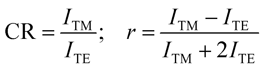 | (1) |
 | ||
| Fig. 5 (a) Far-field polarization-dependent PL intensity measurement setup. Similar to the LCD operation mechanism, the emitted light of isotropic QDs coupled to v-BLU passes through an analyzer and a color filter to reject out laser light. Using a spectrometer, we measure the intensity spectrum at different angles of the analyzer. Laser excitation polarization makes 45° with the grooves direction ensuring equal excitation of both TM and TE polarizations. (b) The absorption and emission spectra of red-emitting (λPL = 620 nm) and green-emitting (λPL = 540 nm) QDs used in this study are shown with the corresponding TM polarization transmission spectra of gold and silver v-BLUs. (c) Maximum and minimum PL spectra of red-emitting and green-emitting QDs in TM and TE polarizations showing high CR and no significant change in the peak wavelength. (d) The analyzer angle-dependent PL intensity for red QDs follows well-defined cos2 dependence with CR = 9.70. The gray spheres are the PL intensity of QDs on flat gold film and the absence of cos2 dependence is an indicator for the absence of measurement system-related anisotropy. (e) The analyzer angle-dependent PL intensity for green QDs follows well-defined cos2 dependence with CR = 4.32. | ||
Gray spheres show the integrated PL intensity of QDs on flat gold film and unity CR indicates that there is no inherent anisotropy coming from the measurement setup. The higher PL intensity value of TM polarization on v-BLU is a combination of higher transmission and increased electric field intensity as shown in Fig. 4. For the green QD-silver structure we have a CR of 4.32 as shown in Fig. 5e, which corresponds to r = 0.53. The observed CR of red QDs coupled to gold v-BLU in steady-state PL is almost two times the expected PL from transmission measurements. This higher CR indicates that the v-BLU does not simply clip the TE polarization emission but enhances the TM polarization emission.
Transient analysis of anisotropic emission
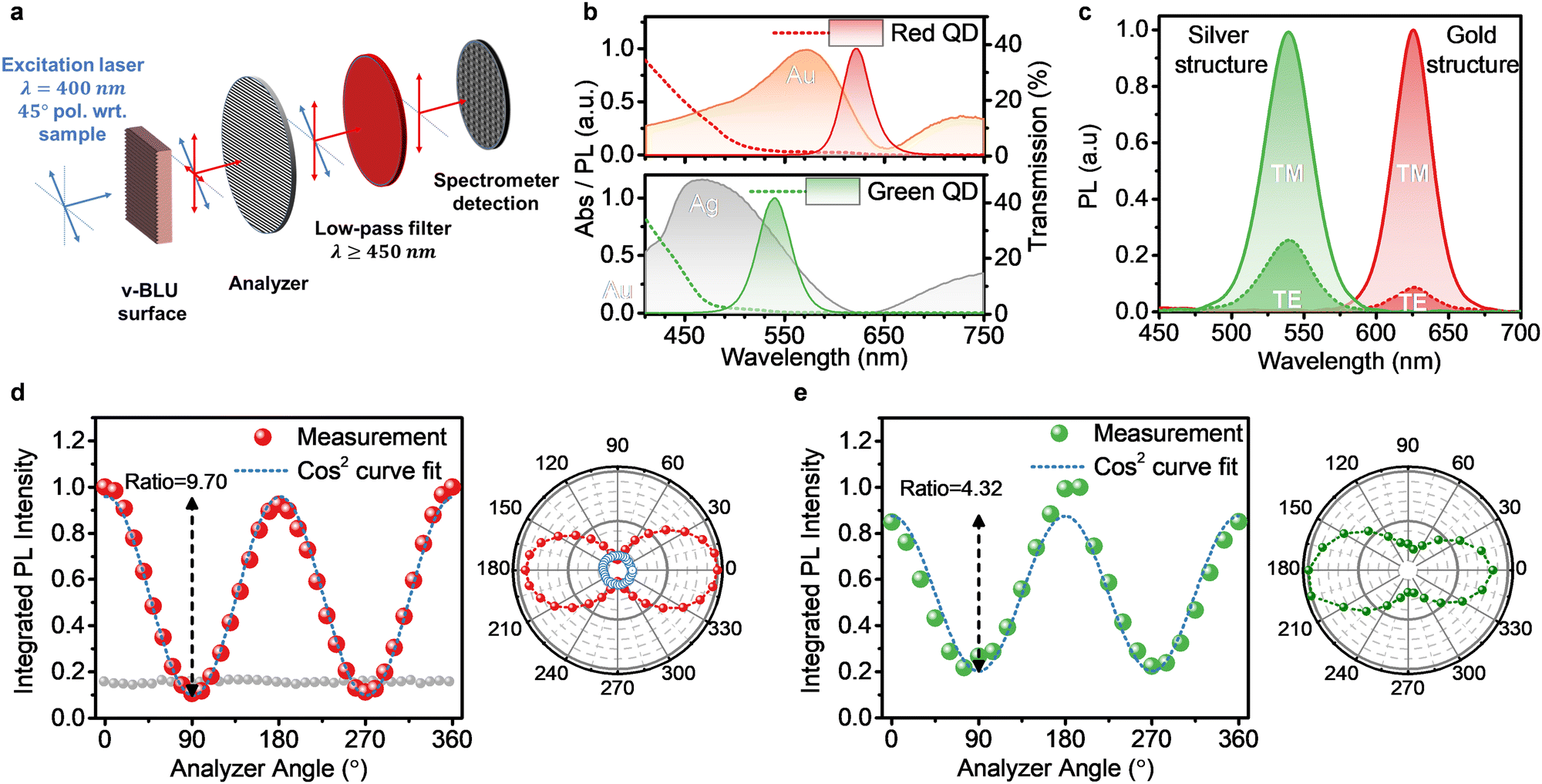
To overcome the loss mechanisms of conventional polarized emission methods, the emission control of emitters is crucial. When a rear polarizer is used, rejecting a specific polarization state of randomly polarized light results in losing half of the intensity. Control over the emission anisotropy of the quantum emitter can prevent these losses and increase the overall efficiency of displays. In the steady-state PL measurements, red QDs on gold v-BLU show a high CR, which cannot be simply explained by polarization selective transmission of v-BLU. There must be a modification mechanism in the optical density of states for QDs in TM and TE polarizations. In Fig. 6a, PL decays of QDs with and without being coupled with v-BLU show a significant change in the PL decay kinetics. QDs without a metallic layer in their proximity have an amplitude-averaged lifetime of 10.1 ± 0.78 ns. Under plasmonic interaction, the lifetime of the QDs reduces to 672 ± 55 ps on the flat gold layer. The TM polarized emission of the QDs on top of the v-BLU has the highest decay rate with a lifetime of 395 ± 18 ps indicating an increased density of optical states since the steady-state PL measurements yielded PL intensity enhancement for TM polarization. This highest decay rate of TM polarization emission can be attributed to the increase in the radiative decay mechanisms for QDs. As expected from the transmission spectra in Fig. 3a and steady-state PL measurements in Fig. 5d, the TE polarization (τavg = 613 ± 67 ps) and QD emission on flat gold (τavg = 672 ps) average lifetimes are similar. In addition to the enhanced TM polarization emission, slightly lower PL intensity level and faster decay rate of TE polarization emission compared to the QDs on flat gold film is an indicator for the strong influence of v-BLU forcing isotropic QDs to emit in a specific polarization orientation. The calculated anisotropy value using these decay curves gives r = 0.76, agreeing well with our steady-state anisotropy measurement of r = 0.74.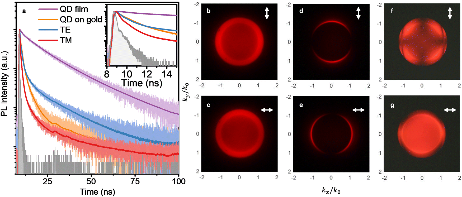 | ||
| Fig. 6 (a) Time-resolved fluorescence analysis of the red QD films shows a strong modification in the density of optical states for QDs. While the average lifetime of plain QD film is 10.08 ns, the decay rate increases when QDs are in proximity of the gold layer (for QDs on plain gold layer τav = 0.70 ns). The increased PL intensity and the fastest decay (τav = 0.39 ns) observed in the TM-polarization PL of QDs indicate a pronounced anisotropy which is measured as 0.76 from transient analysis, agreeing well with the steady-state measurements. The inset figure zooms into the initial time window of the decay curves and shows a similar transient response for TE-polarization and plain gold film emissions. The gray curve corresponds to the instrument response function of our measurement system. Emitter dipole orientations of red-emitting QDs under different configurations are measured using back focal plane imaging: (b) and (c) QD film on fused silica, (d) and (e) QD film on plain gold layer and (f) and (g) QD film on gold v-BLU. QDs on fused silica and plain gold are isotropic for different analyzer orientations. On v-BLU, different BFP images for perpendicular analyzer orientations indicate that emission is coming from an orientated dipole. When analyzer orientation is aligned with dominant polarization emission is allowed to pass (g). | ||
Dipole orientation of anisotropy-enforced isotropic QDs
Pronounced anisotropy in QD emission as a result of the anisotropic modification in the optical density of states is expected to change the emitter dipole orientation. Back focal plane (BFP) imaging can be used to observe the dipole orientations of anisotropic emitters.51–54 In Fig. 6b–g, BFP images of plain red QD film on fused silica, red QD film on plain gold layer and red QDs on gold v-BLU are shown under two perpendicular analyzer orientations. The plain QD film on fused silica has similar BFP images (Fig. 6b and c) under different polarizations, showing isotropic emission with a central spot surrounded by a brighter ring. The ring shape is due to the critical angle and its Fourier space radius is close to k0, where k0 is the free space wavenumber of the electromagnetic radiation. Considering the effective refractive indices of the QD film (neff ≅ 1.8)12 and fused silica layer, the theoretical radius of 0.81 k0 is close to the observed ring radius in the BFP image. The QD film on the plain gold layer (Fig. 6d and e) shows a characteristic SPCE narrow ring shape as a result of the strong angle-dependent directional emission at the SPP coupling angle.55 It is reciprocal to the Kretschmann configuration of SPP excitation: instead of exciting SPPs in gold film with a monochromatic light source impinging at a specific angle, QD emission is coupled to SPPs and radiation is observed at the SPP angle at the backplane of the gold film. Since only TM polarization can excite SPPs, the SPCE of the QD film is highly polarization dependent. However, TM polarization is dependent on the reference frame for the plain gold film and this reference frame is dictated by the analyzer orientation: when the analyzer is rotated, the rejected portion of TM polarization emission is rotated as well. In Fig. 6f and g, distinctly different BFP images of QDs coupled to gold v-BLU for two orthogonal analyzer orientations suggest strong polarization dependent emission. The BFP pattern in Fig. 6f is typical for anisotropic emitters when the analyzer orientation is perpendicular to the emitter dipole orientation and previously reported for anisotropic molecular emitters.56 An illustration of this anisotropic BFP pattern formation mechanism is presented in Fig. S3 in the ESI.† In contrast to SPCE behavior, v-BLU fixes the reference frame for the dipole orientation and angled walls of the grooves eliminate the undesired directional oblique emission observed in SPCE. We observe a central spot in the v-BLU coupled BFP image of QDs indicating a surface-normal emission, which is an important and desired feature for LCD operation.v-BLU used as a rear polarized emitter in a proof-of-concept display application
A proof-of-concept LCD application was realized by using red QD-gold v-BLU in the backplane replacing the rear polarizer. The fabricated bendable gold v-BLU with red QDs is shown in Fig. 7a. The structure consists of a thin gold layer, a micrometer thick supporting PMMA polymer layer and Scotch tape used in stripping off the replicate. To further eliminate the possibility of measurement system related anisotropies, we fabricated two structures on the same substrate with perpendicular groove orientations. With a spin-deposited red QD layer, the resulting complete structure is bendable and light-weight. In Fig. 7b, v-BLU with a thick QD layer (CR = 5.6) is imaged through an analyzer, with UV back illumination and under ambient lighting. On and off behavior is realized by rotating the analyzer. At 45°, both QD emission and plasmonic structure reflection is similar for both structures. Finally, by disintegrating a transparent LCD clock, we fabricated a display using our red QD v-BLU. We kept the LCD unit and front polarizer but replaced the rear polarizer with our v-BLU. Since the size was matching with the dimensions of our structures, we used “DATE” writing on the clock in a similar configuration as illustrated in Fig. 1. Under orthogonal orientations of the rear polarizer, bright and dark areas of the writing interchanges as shown in Fig. 7c and d. Under UV illumination from the backplane, our v-BLU structures with perpendicular orientations realize both configurations of the writing as shown in Fig. 7e. It is remarkable that the letters are only visible in the areas where v-BLU structures are defined, proving that display operation originates from genuine polarized light generated by v-BLU. | ||
| Fig. 7 (a) Fabricated bendable v-BLUs under ambient lighting. On the same film there are two structures with perpendicular groove orientations to minimize measurement system related anisotropies. (b) Analyzer orientation dependent photographs of two structures on the same substrate: QD PL emission with UV back-illumination and reflection of the structure under ambient lighting. Orthogonal orientations of the analyzer turn on and off each structure. At 45° the responses of both structures are the same. (c) Rear polarizer orientation dependent letters on a transparent LCD clock are shown to exemplify display operation. The background is bright, and the letters are dark when the front and rear polarizers are parallel. (d) The bright and dark areas are interchanged when the front and rear polarizers are perpendicular. (e) “DATE” writing is created using gold v-BLU used as back illumination replacing the rear polarizer. Both configurations observed in (c) and (d) for orthogonal orientations of v-grooves on the same substrate. Letters are only visible on the structures indicating display operation enabled by the polarized light converted from v-BLUs. | ||
Conclusions
Producing polarized light emission from isotropic QDs opens new possibilities for next-generation displays. The proposed v-BLU plasmonic surface modifies the optical density of states of the QDs and forces them to emit anisotropically. Control over the decay kinetics and dipole orientation of these isotropic QDs is instrumental to overcome optical losses caused by the rear polarizer in conventional LCDs. The fabrication method developed for the v-BLU here allows for a bendable and polarized light generating color-converting backplane illumination unit for LCDs. The proof-of-concept display demonstration using the QD-v-BLU architecture supports the feasibility for their practical display applications. As a future outlook it is possible to fabricate polarized LEDs using isotropic QDs as an active layer with the v-BLU structure embedded. In such, with an appropriate material choice, continuous metallic film of v-BLU can act like one of the contact layers and induce anisotropy for the optical density of states for QDs. In this respect, v-BLU is a promising platform for future displays.Although the proposed v-BLU suggests significant improvement of the energy efficiency by disabling the emission of the undesired polarization, the illumination efficiency can be further maximized by tuning parameters such as QD film thickness, gold film thickness and possibly through the addition of a spacer layer between the QD and gold layer, whose thickness should also be carefully tuned to optimize not only the plasmonic enhancement but also the transmittance of the v-BLUs. These multiple degrees of freedom present the possibility of further increasing the energy efficiency of our proof-of-concept backlight units.
Polarized QD emitter-based backlight units for LCDs present a technologically feasible and scalable approach. The bottleneck in the fabrication is the production of the master substrate for the v-groove structure as the rest of the fabrication steps including PDMS replica production and conformal QD coating involve scalable solution processing methods. Considering the accelerated improvements in deep UV lithography tools enabling sub-micrometer patterning, in line with the dimensions of our v-groove structures, we anticipate that large area master substrates can be rapidly fabricated for small (1–30 cm) area displays. Alternatively, smaller master substrates can be patched together to produce large area films needed for large-format TV screens.
Methods
Fabrication of v-BLU
Optical characterizations
Polarization dependent optical transmission measurements were carried out using an Agilent Cary 60 UV-Vis spectrophotometer to eliminate the possibility of exciting QDs which could otherwise disturb the transmission spectra with their photoluminescence. A polarizer was placed after the excitation source and a template-stripped PMMA layer from the flat silicon surface was used for baseline measurements.Steady-state polarization dependent PL measurements were performed under linearly polarized CW laser excitation at 400 nm. The polarization of the laser was 45° with respect to the groove orientations to ensure the equal excitation of both modes. A linear polarizer was placed as the analyzer after the sample. A low-pass filter eliminating the laser excitation was placed before the collecting fiber connected to the Maya 2000 spectrometer from Ocean Optics.
Transient PL analyses of the v-BLUs were carried out with a time-correlated single-photon counting system PicoHarp 300 from PicoQuant. Samples were placed in parallel with the detector window to eliminate the anisotropy, which could arise from obliquely collected photons. The analyzer was placed after the samples in the optical path. Anisotropy and related G-factor measurement configurations are illustrated in Fig. S1 and S2 in the ESI.†
Back focal plane imaging was carried out using a Nikon TiU inverted microscope and 100 × 1.3 NA oil immersion objective. Laser excitation was provided on the sample from the opposite side of the collection. In the collection end, a Bertrand lens (achromatic lens AC254-100-A-ML from Thorlabs) and a charge-coupled detector camera was used as shown in Fig. S4 in the ESI.†
Numerical simulations
Two-dimensional FDTD simulations of gold and silver v-BLUs were performed using FDTD solutions from Lumerical. The unit cell with a period of 200 nm was simulated with periodic boundary conditions on the two sides of the unit cell in the x-direction as indicated in Fig. 4. After careful convergence tests, a mesh override region was defined to fix meshes around v-BLU with mesh sizes of Δx = 1 nm and Δy = 2 nm. TM and TE polarizations were modeled with a change in the source polarization. Broadband plane wave injection was used for both gold and silver v-BLUs. In silver v-BLU simulations, small cylinders were placed at the sharp corners to simulate the rounded corners of the silver structure occurring during the fabrication. Metallic layer refractive index values were obtained using ellipsometry measurements of template-stripped gold and silver films from a silanized flat silicon wafer surface.Abbreviations
| BFP | back focal plane |
| CR | (polarization) contrast ratio |
| FDTD | finite-difference time-domain |
| LCC | liquid crystal cell |
| LCD | liquid crystal display |
| PL | photoluminescence |
| PMMA | polymethylmethacrylate |
| QD | quantum dot |
| SPCE | surface plasmon coupled emission |
| SPP | surface plasmon polariton |
| TE | transverse electric |
| TM | transverse magnetic |
Author contributions
K. G., B. G., and H. V. D. conceived the idea. K. G. designed, numerically simulated, and fabricated the structures. K. G. characterized the structures with the help of O. E. for the transient PL analysis. S. J. and E. J. provided the QDs. K. G. wrote the manuscript through contributions of all authors.Data availability
All data used in this study are available within the article and its ESI.†Conflicts of interest
There are no conflicts to declare.Acknowledgements
The authors gratefully acknowledge the financial support from the Samsung GRO Program. H. V. D. acknowledges support from TUBA (Turkish Academy of Sciences). K. G. and O. E. acknowledge support from TUBITAK BIDEB.References
- J. M. Pietryga, Y. S. Park, J. Lim, A. F. Fidler, W. K. Bae, S. Brovelli and V. I. Klimov, Chem. Rev., 2016, 116, 10513–10622 CrossRef CAS PubMed.
- S. Kim and M. G. Bawendi, J. Am. Chem. Soc., 2003, 125, 14652–14653 CrossRef CAS PubMed.
- B. G. Jeong, Y. S. Park, J. H. Chang, I. Cho, J. K. Kim, H. Kim, K. Char, J. Cho, V. I. Klimov, P. Park, D. C. Lee and W. K. Bae, ACS Nano, 2016, 10, 9297–9305 CrossRef CAS PubMed.
- E. Jang, S. Jun, H. Jang, J. Lim, B. Kim and Y. Kim, Adv. Mater., 2010, 22, 3076–3080 CrossRef CAS PubMed.
- V. Wood and V. Bulović, Nano Rev., 2010, 1, 5202 CrossRef PubMed.
- T. H. Kim, K. S. Cho, E. K. Lee, S. J. Lee, J. Chae, J. W. Kim, D. H. Kim, J. Y. Kwon, G. Amaratunga, S. Y. Lee, B. L. Choi, Y. Kuk, J. M. Kim and K. Kim, Nat. Photonics, 2011, 5, 176–182 CrossRef CAS.
- Y. Wang, I. Fedin, H. Zhang and D. V. Talapin, Science, 2017, 357, 385–388 CrossRef CAS PubMed.
- T. Erdem and H. V. Demir, Nat. Photonics, 2011, 5, 126 CrossRef CAS.
- T. Erdem, S. Nizamoglu, X. W. Sun and H. V. Demir, Opt. Express, 2010, 18, 340–347 CrossRef CAS PubMed.
- S. Nizamoglu, T. Ozel, E. Sari and H. V. Demir, Nanotechnology, 2007, 18(6), 065709 CrossRef.
- S. Nizamoglu, G. Zengin and H. V. Demir, Appl. Phys. Lett., 2008, 92(3), 031102 CrossRef.
- B. T. Diroll, E. A. Gaulding, C. R. Kagan and C. B. Murray, Chem. Mater., 2015, 27, 6463–6469 CrossRef CAS.
- Nat. Nanotechnol., 2014, 9, 325 Search PubMed.
- K. Bourzac, Nature, 2013, 493, 283 CrossRef CAS PubMed.
- H. Chen, J. He and S.-T. Wu, IEEE J. Sel. Top. Quantum Electron., 2017, 23(5), 1900611 Search PubMed.
- Z. Luo, J. Manders and J. Yurek, IEEE Spectrum, 2018, 55, 28–35 Search PubMed.
- E. Jang, S. Jun, H. Jang, J. Lim, B. Kim and Y. Kim, Adv. Mater., 2010, 22, 3076–3080 CrossRef CAS PubMed.
- J. Hu, L. Li, W. Yang, L. Manna, L.-W. Wang and A. P. Alivisatos, Science, 2001, 292, 2060–2063 CrossRef CAS PubMed.
- R. A. M. Hikmet, P. T. K. Chin, D. V. Talapin and H. Weller, Adv. Mater., 2005, 17, 1436–1439 CrossRef CAS PubMed.
- P. D. Cunningham, J. B. Souza, I. Fedin, C. She, B. Lee and D. V. Talapin, ACS Nano, 2016, 10, 5769–5781 CrossRef CAS PubMed.
- H. K. Fu, C. W. Chen, C. H. Wang, T. T. Chen and Y. F. Chen, Opt. Express, 2008, 16, 6361–6367 CrossRef CAS PubMed.
- M. Ma, D. S. Meyaard, Q. Shan, J. Cho, E. Fred Schubert, G. B. Kim, M. H. Kim and C. Sone, Appl. Phys. Lett., 2012, 101(6), 061103 CrossRef.
- L. Zhang, J. H. Teng, S. J. Chua and E. A. Fitzgerald, Appl. Phys. Lett., 2009, 95, 2007–2010 Search PubMed.
- R. Oulton, B. D. Jones, S. Lam, A. R. A. Chalcraft, D. Szymanski, D. O’Brien, T. F. Krauss, D. Sanvitto, A. M. Fox, D. M. Whittaker, M. Hopkinson and M. S. Skolnick, Opt. Express, 2007, 15, 17221 CrossRef CAS PubMed.
- T. Ming, L. Zhao, H. Chen, K. C. Woo, J. Wang and H. Q. Lin, Nano Lett., 2011, 11, 2296–2303 CrossRef CAS PubMed.
- C. Uran, T. Erdem, B. Guzelturk, N. K. Perkgöz, S. Jun, E. Jang and H. V. Demir, Appl. Phys. Lett., 2014, 105(14), 141116 CrossRef.
- M. Ren, M. Chen, W. Wu, L. Zhang, J. Liu, B. Pi, X. Zhang, Q. Li, S. Fan and J. Xu, Nano Lett., 2015, 15, 2951–2957 CrossRef CAS PubMed.
- E. De Leo, A. Cocina, P. Tiwari, L. V. Poulikakos, P. Marqués-Gallego, B. Le Feber, D. J. Norris and F. Prins, ACS Nano, 2017, 11, 12167–12173 CrossRef CAS PubMed.
- T. Ozel, S. Nizamoglu, M. A. Sefunc, O. Samarskaya, I. O. Ozel, E. Mutlugun, V. Lesnyak, N. Gaponik, A. Eychmuller, S. V. Gaponenko and H. V. Demir, ACS Nano, 2011, 5, 1328–1334 CrossRef CAS PubMed.
- J. R. Lakowicz, J. Malicka, I. Gryczynski and Z. Gryczynski, Biochem. Biophys. Res. Commun., 2003, 307, 435–439 CrossRef CAS PubMed.
- I. Gryczynski, J. Malicka, W. Jiang, H. Fischer, W. C. W. Chan, Z. Gryczynski, W. Grudzinski and J. R. Lakowicz, J. Phys. Chem. B, 2005, 109, 1088–1093 CrossRef CAS PubMed.
- F. Balli, M. Sultan, S. K. Lami and J. T. Hastings, Nat. Commun., 2020, 11, 1–8 CrossRef PubMed.
- A. M. Baracu, M. A. Avram, C. Breazu, M. C. Bunea, M. Socol, A. Stanculescu, E. Matei, P. C. V. Thrane, C. A. Dirdal, A. Dinescu and O. Rasoga, Nanomaterials, 2021, 11, 1–17 CrossRef PubMed.
- A. I. Kuznetsov, A. E. Miroshnichenko, M. L. Brongersma, Y. S. Kivshar and B. Luk’yanchuk, Science, 2016, 354, aag2472 CrossRef PubMed.
- L. Ding, D. Morits, R. Bakker, S. Li, D. Eschimese, S. Zhu, Y. F. Yu, R. Paniagua-Dominguez and A. I. Kuznetsov, ACS Photonics, 2020, 7, 1001–1008 CrossRef CAS.
- L. Sun, Y. Zhang, Y. He, H. Wang and Y. Su, Nanophotonics, 2020, 9, 1321–1340 CrossRef CAS.
- Y. Meng, Y. Chen, L. Lu, Y. Ding, A. Cusano, J. A. Fan, Q. Hu, K. Wang, Z. Xie, Z. Liu, Y. Yang, Q. Liu, M. Gong, Q. Xiao, S. Sun, M. Zhang, X. Yuan and X. Ni, Light: Sci. Appl., 2021, 10, 1–44 CrossRef PubMed.
- F. Prins, D. K. Kim, J. Cui, E. De Leo, L. L. Spiegel, K. M. McPeak and D. J. Norris, Nano Lett., 2017, 17, 1319–1325 CrossRef CAS PubMed.
- W. Mei, Z. Zhang, A. Zhang, D. Li, X. Zhang, H. Wang, Z. Chen, Y. Li, X. Li and X. Xu, Nano Res., 2020, 13, 2485–2491 CrossRef CAS.
- X. Fu, Y. Mehta, Y. A. Chen, L. Lei, L. Zhu, N. Barange, Q. Dong, S. Yin, J. Mendes, S. He, R. Gogusetti, C. H. Chang and F. So, Adv. Mater., 2021, 33, 1–10 Search PubMed.
- M. Hegner, P. Wagner and G. Semenza, Surf. Sci., 1993, 291, 39–46 CrossRef CAS.
- D. Qin, Y. Xia and G. M. Whitesides, Nat. Protoc., 2010, 5, 491–502 CrossRef CAS PubMed.
- P. Nagpal, N. C. Lindquist, S.-H. Oh and D. J. Norris, Science, 2009, 325, 594–597 CrossRef CAS PubMed.
- S. Jun, E. Jang and J. E. Lim, Nanotechnology, 2006, 17, 3892–3896 CrossRef CAS.
- S. Maier, Plasmonics: fundamentals and applications, Springer, 2007 Search PubMed.
- R. Nicolas, G. Lévêque, J. Marae-Djouda, G. Montay, Y. Madi, J. Plain, Z. Herro, M. Kazan, P. M. Adam and T. Maurer, Sci. Rep., 2015, 5, 1–11 Search PubMed.
- M. F. Limonov, M. V. Rybin, A. N. Poddubny and Y. S. Kivshar, Nat. Photonics, 2017, 11, 543–554 CrossRef CAS.
- G. D’Aguanno, N. Mattiucci, M. J. Bloemer, D. de Ceglia, M. A. Vincenti and A. Alù, J. Opt. Soc. Am. B, 2011, 28, 253 CrossRef.
- A. Lovera, B. Gallinet, P. Nordlander and O. J. F. Martin, ACS Nano, 2013, 7, 4527–4536 CrossRef CAS PubMed.
- B. Luk’Yanchuk, N. I. Zheludev, S. A. Maier, N. J. Halas, P. Nordlander, H. Giessen and C. T. Chong, Nat. Mater., 2010, 9, 707–715 CrossRef PubMed.
- J. A. Schuller, S. Karaveli, T. Schiros, K. He, S. Yang, I. Kymissis, J. Shan and R. Zia, Nat. Nanotechnol., 2013, 8, 271–276 CrossRef CAS PubMed.
- Y. Gao, M. C. Weidman and W. A. Tisdale, Nano Lett., 2017, 17, 3837–3843 CrossRef CAS PubMed.
- R. Scott, J. Heckmann, A. V. Prudnikau, A. Antanovich, A. Mikhailov, N. Owschimikow, M. Artemyev, J. I. Climente, U. Woggon, N. B. Grosse and A. W. Achtstein, Nat. Nanotechnol., 2017, 12, 1155–1160 CrossRef CAS PubMed.
- L. Novotny and B. Hecht, Principles of Nano-Optics, Cambridge University Press, New York, 2006 Search PubMed.
- D. Zhang, R. Badugu, Y. Chen, S. Yu, P. Yao, P. Wang, H. Ming and J. R. Lakowicz, Nanotechnology, 2014, 25, 145202 CrossRef PubMed.
- A. S. Backer, M. P. Backlund, M. D. Lew and W. E. Moerner, Opt. Lett., 2013, 38, 1521–1523 CrossRef PubMed.
Footnote |
| † Electronic supplementary information (ESI) available: In-film anisotropy measurement setup configuration using time-resolved fluorescence spectroscopy is illustrated. Back focal plane imaging of emitter dipoles and aligned dipole characteristic BFP pattern formation illustration and BFP setup used in this work is presented. See DOI: https://doi.org/10.1039/d4nh00101j |
| This journal is © The Royal Society of Chemistry 2024 |