
 Open Access Article
 This Open Access Article is licensed under a
 Creative Commons Attribution 3.0 Unported Licence
Control of Ge island coalescence for the formation of nanowires on silicon†
Santhanu Panikar
Ramanandan
 a,
Joel
Reñé Sapera
a,
Alban
Morelle
b,
Sara
Martí-Sánchez
c,
Alok
Rudra
ad,
Jordi
Arbiol
ce,
Vladimir G.
Dubrovskii
f and
Anna
Fontcuberta i Morral
*adg
a,
Joel
Reñé Sapera
a,
Alban
Morelle
b,
Sara
Martí-Sánchez
c,
Alok
Rudra
ad,
Jordi
Arbiol
ce,
Vladimir G.
Dubrovskii
f and
Anna
Fontcuberta i Morral
*adg
aLaboratory of Semiconductor Materials, Institute of Materials, Ecole Polytechnique Fédérale de Lausanne EPFL, Lausanne 1015, Switzerland. E-mail: anna.fontcuberta-morral@epfl.ch
bSolid State Laboratory, ETH Zurich, 8093 Zurich, Switzerland
cCatalan Institute of Nanoscience and Nanotechnology (ICN2), CSIC and BIST, Campus UAB, Bellaterra, Barcelona, Catalonia, Spain
dInstitute of Physics, Faculty of Basic Sciences, Ecole Polytechnique Fédérale de Lausanne EPFL, Lausanne 1015, Switzerland
eICREA, Pg. Lluís Companys 23, 08010 Barcelona, Catalonia, Spain
fFaculty of Physics, St. Petersburg State University, Universitetskaya Embankment 13B, 199034 St. Petersburg, Russia
gCenter for Quantum Science and Engineering, École Polytechnique Fédérale de Lausanne (EPFL), CH-1015 Lausanne, Switzerland
First published on 12th February 2024
Abstract
Germanium nanowires could be the building blocks of hole-spin qubit quantum computers. Selective area epitaxy enables the direct integration of Ge nanowires on a silicon chip while controlling the device design, density, and scalability. For this to become a reality, it is essential to understand and control the initial stages of the epitaxy process. In this work, we highlight the importance of surface treatment in the reactor prior to growth to achieve high crystal quality and connected Ge nanowire structures. In particular, we demonstrate that exposure to AsH3 during the high-temperature treatment enhances lateral growth of initial Ge islands and promotes faster formation of continuous Ge nanowires in trenches. The Kolmogorov–Johnson–Mehl–Avrami crystallization model supports our explanation of Ge coalescence. These results provide critical insight into the selective epitaxy of horizontal Ge nanowires on lattice-mismatched Si substrates, which can be translated to other material systems.
New conceptsThe selective area epitaxy approach (SAE) has emerged as a means of directly organizing nanowires at the location of future devices in a scalable manner. Realizing this potential requires a complete understanding and control of the initial stages of the epitaxy process. This study reveals, for the first time, the underlying growth mechanism of Ge nanowires during selective area epitaxy and the origin of crystal imperfections. Highlighting the crucial role of pre-growth surface treatment, our results demonstrates that exposure to AsH3 during pre-growth surface treatment enhances the lateral growth of initial Ge islands, resulting in a faster formation of continuous nanowires. It also minimizes defect formation. Furthermore, the application of the 2D Kolmogorov–Johnson–Mehl–Avrami (KJMA) crystallization model accurately captures the growth kinetics of island coalescence during SAE, supporting our explanations. These results provide essential insights into the selective epitaxy of horizontal Ge nanowires on lattice-mismatched Si substrates, which can be applied to other material systems. |
1 Introduction
Site-selective integration of nanowires on a host substrate is essential for the scalability of nanowire devices.1,2 In recent years, the selective area epitaxy (SAE) approach has emerged as a means of precisely arranging nanowires in the locations of future devices in a scalable and deterministic manner. This technique uses openings created in a crystalline substrate covered with a mask to obtain nanowires of different geometries. The mask, typically made of oxide material to which growth precursors do not adhere at the growth temperature, restricts nanowire growth to the unmasked regions of the substrate.3–7Compared with conventional free-standing nanowire growth,8–13 the SAE approach offers several advantages.14 Firstly, the SAE process allows for the direct growth of the nanostructures in locations of future devices. Secondly, the design flexibility of the SAE approach enables the integration of nanoscale devices of varying size and complexity at a wafer scale.15,16 Finally, the small interface area between the grown semiconductor and the host substrate limits the formation of interface-related defects, enabling the integration of lattice-mismatched materials.17,18 Because of these convenient properties, the SAE approach has been the subject of rapidly increasing interest in the area of electronic and quantum computing applications.17,19,20
Among the material platforms available for quantum technologies, holes in Ge nanowires are promising for spin-qubit based quantum computing. This is due to their strong spin–orbit interaction (SOI) and low susceptibility to hyperfine interaction.21–23 The strong SOI of holes facilitates fast, electrical manipulation of qubits, while the low susceptibility to hyperfine interactions guarantees long coherence lifetimes. The use of the SAE approach in growing Ge nanowires offers control over the crystalline shape and orientation to cancel out the impact of charge noise and hyperfine interaction on coherence.24 Our previous work has demonstrated the SAE of in-plane Ge nanowires and their networks on Si (001) substrates.4 Low-temperature electronic transport measurements on nanowire Hall bar devices showed coherent hole transport and a weak anti-localization peak, indicating strong SOI.
This work illuminates the underlying growth mechanism of Ge nanowires in SAE and the origin of crystal imperfections, such as dislocations and stacking faults. It also provides a path to minimizing defect formation. While similar studies have previously explored the SAE of III–V,25–27 II–V,28,29 and IV–VI7,30 compounds, to the best of our knowledge there is no available report on the SAE of Ge nanowires on Si. The SAE of Ge nanowires on Si (001) substrates proceeds through the nucleation and coalescence of Ge islands. We study the effect of the in situ surface pretreatment step on the coalescence and crystalline quality of the Ge nanowires. The Kolmogorov–Johnson–Mehl–Avrami's (KJMA) 2D crystallization model is used to capture the growth kinetics of the coalescence process. Finally, we compare the crystal quality and investigate the origin of defects in Ge nanowires using aberration-corrected scanning transmission electron microscopy (STEM). From this point of view, the present study provides a critical insight into the SAE of horizontal Ge nanowires on Si substrates that can be translated to other materials systems.
2 Experimental procedures
Fig. 1a shows a schematic illustration of the SAE process. We start with an intrinsic Si (001)/SiO2 substrate with nanoscale trenches defined along the 〈110〉 crystallographic direction. The substrates investigated in this study consist of an array of 10 parallel nanoscale trenches with a length of 20 μm and a center-to-center spacing of 1 μm. Details of the substrate patterning procedure are provided in our previous publication4 and in the ESI.† The substrates are briefly etched in dilute HF solution (1![[thin space (1/6-em)]](https://www.rsc.org/images/entities/char_2009.gif) :100 dilution with H2O) to remove the native surface oxide of silicon inside the trenches and transferred into an Aixtron 200 MOVPE system. The Ge nanowire growth recipe begins with an annealing step at 820 °C – the maximum temperature achievable in our system – to ensure a clean surface inside the nanoscale trenches. From here on, we call this the surface pretreatment step. After the surface pretreatment step, the substrates are cooled down under N2 in the absence of AsH3 to the nanowire growth temperature of 750 °C in 4 minutes. All growths mentioned in this work are carried out at 30 mbar pressure using isobutyl germane (IBuGe) as the Ge precursor and N2 as the carrier gas. The partial pressure of IBuGe is adjusted to deliver a nominal growth rate of 1 nm min−1 as calibrated separately on planar GaAs substrates. The growth time varies from 2.5 s to 110 s to obtain the temporal evolution of Ge nanowire growth inside the trenches.
:100 dilution with H2O) to remove the native surface oxide of silicon inside the trenches and transferred into an Aixtron 200 MOVPE system. The Ge nanowire growth recipe begins with an annealing step at 820 °C – the maximum temperature achievable in our system – to ensure a clean surface inside the nanoscale trenches. From here on, we call this the surface pretreatment step. After the surface pretreatment step, the substrates are cooled down under N2 in the absence of AsH3 to the nanowire growth temperature of 750 °C in 4 minutes. All growths mentioned in this work are carried out at 30 mbar pressure using isobutyl germane (IBuGe) as the Ge precursor and N2 as the carrier gas. The partial pressure of IBuGe is adjusted to deliver a nominal growth rate of 1 nm min−1 as calibrated separately on planar GaAs substrates. The growth time varies from 2.5 s to 110 s to obtain the temporal evolution of Ge nanowire growth inside the trenches.
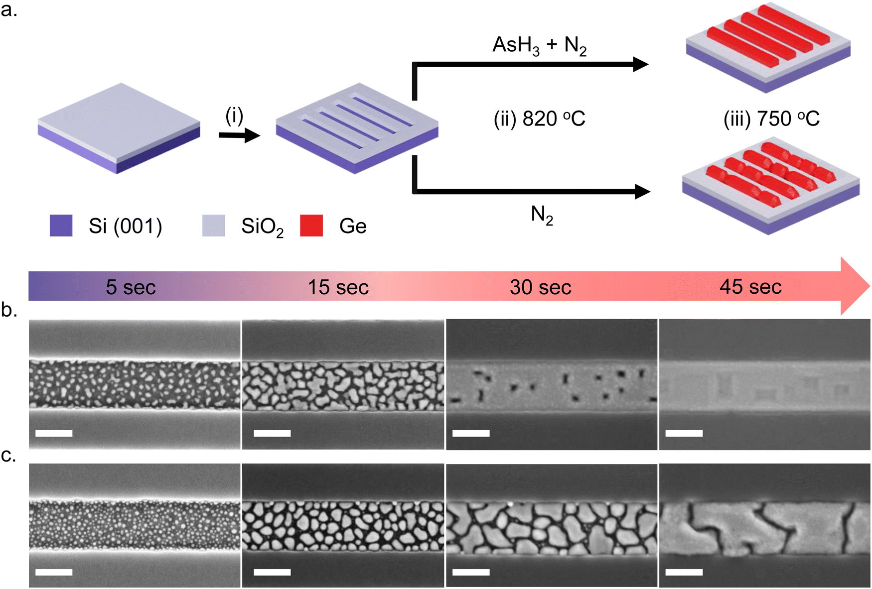 | ||
| Fig. 1 (a) Schematic illustration of the SAE process by MOVPE: (i) substrate patterning step to define trenches in the SiO2 mask, (ii) surface pretreatment step at 820 °C to ensure a clean Si (001) surface and (iii) Ge nanowire growth at 750 °C. Nucleation and coalescence of Ge islands during SAE: top view SEM images showing different stages of Ge film growth inside a 250 nm wide trench on Si (001) surface obtained after the surface pretreatment step (b) with and (c) without AsH3. The scale bar shown in (b) and (c) indicates 200 nm. | ||
We investigate the effect of the surface pretreatment step on the SAE of Ge by comparing two different procedures. In the first case, the surface pretreatment occurs under AsH3 flow (60 sccm) diluted in N2 (3500 sccm). In the second case, the substrate pretreatment is performed under N2 flow (3500 sccm) without AsH3. The process is summarized in Fig. 1a. Using scanning electron microscopy (SEM), atomic force microscopy (AFM), and transmission electron microscopy (TEM), we compare the time evolution and crystalline quality of germanium nanowires obtained on a Si (001) surface with the two different surface pretreatment procedures.
3 Results and discussion
Fig. 1 describes the growth behavior of Ge inside the trenches as a function of the growth time and the surface pretreatment step. The top view SEM images in Fig. 1b and c depict the time evolution of Ge growth inside a 250 nm wide trench obtained after the surface pretreatment step with and without AsH3, respectively. We provide overview SEM images from the whole array in the ESI† (Fig. S2). Irrespective of the surface pretreatment procedure, the SAE of Ge initiates through the nucleation of multiple small islands inside the trenches, as visible in the SEM images (Fig. 1b and c) after 5 s of growth. However, the surface pretreatment procedure influences the nucleation density and the coalescence process of the Ge islands. Introducing AsH3 during the surface pretreatment step (Fig. 1b) lowers the surface density of Ge islands obtained after 5 s of growth. As growth progresses, the Ge islands expand in volume and coalesce, initially forming Ge films with holes. Finally, the holes fill to create continuous Ge films inside the trench over 45 s of growth. A similar growth behavior was observed during the selective growth of Ge on micrometer-sized Si pillars in ref. 31. On the other hand, omitting AsH3 during the surface pretreatment step (Fig. 1c) results in a higher density of initial Ge islands after 5 s of growth. As the deposition continues, the Ge islands merge to form larger but more compact islands. However, after 45 s of growth, the overlapping islands no longer merge thereby forming a discontinuous film.In order to shed more light on the difference in the time evolution of Ge growth, we model the coalescence process of Ge islands. Growth modeling of thin films starting from three-dimensional (3D) islands, that rapidly coalesce into continuous film inside the trenches in SAE, is not a simple problem because the morphology of the film in the coalescence stage cannot be described in terms of the size, shape, and surface density of individual islands. Solid-like coalescence of crystal islands is usually treated using the KJMA crystallization model.32–34 In the case of two-dimensional (2D) crystallization,35,36 it provides the time-dependent surface coverage θ(t) and perimeter of the crystallization front per unit area of the surface P(t) explicitly. A schematic illustration of the 2D KJMA model is shown in Fig. 2a.
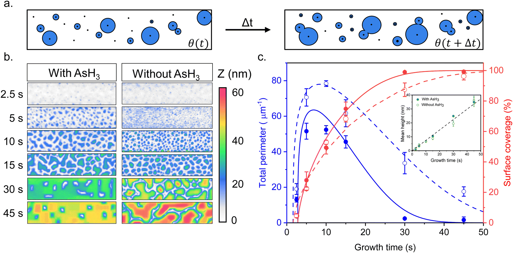 | ||
| Fig. 2 (a) Schematic illustration of the KJMA crystallization model. (b) AFM contour plots comparing the time evolution of a growing Ge film inside the trenches as a function of surface pretreatment conditions. (c) Perimeter per surface area (blue color) and surface coverage (red color) of Ge film grown by MOVPE inside the patterned oxide trenches on Si (001) surface with (filled circle) and without (empty circle) AsH3 during the surface pretreatment step, fitted by the model (solid lines) with the parameters summarized in Table 1. The inset figure shows the time evolution of the mean height of the Ge film inside the trenches. | ||
The general expressions of the KJMA model are given by
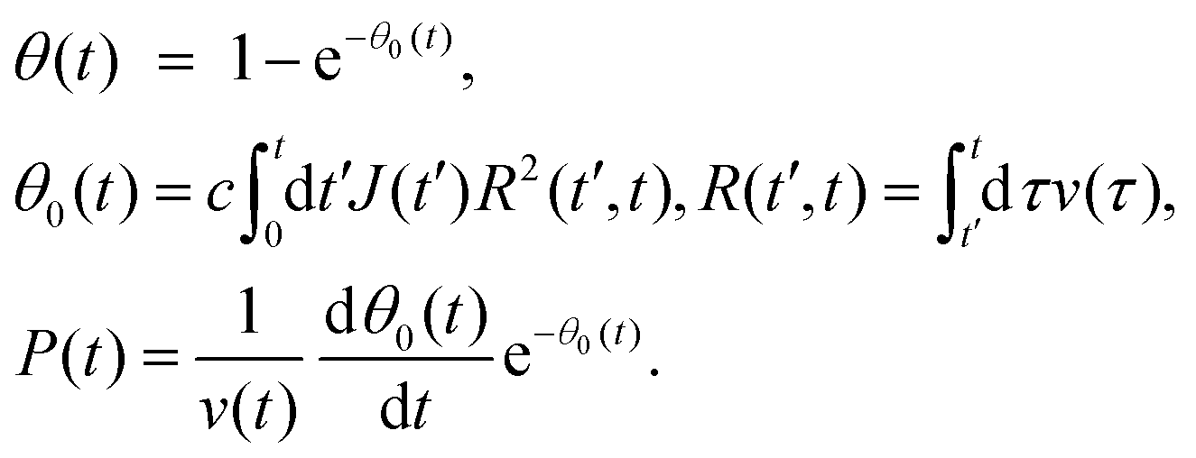 | (1) |
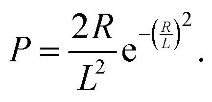
Here, J(t) is the nucleation rate, v(t) is the lateral growth rate of Ge islands, R(t′,t) is the linear size of the island base at time t for an island nucleating (with zero size) at time t′, c is a 2D shape constant and θ0(t) is the extended filling factor which would be observed on a surface if all the merged Ge islands were again separated.32–35,37v(t) is the lateral growth rate of Ge islands.
We use this model to understand the growth kinetics of Ge films shown in Fig. 1 in terms of the time-dependent mean height H(t), perimeter P(t), and coverage θ(t) of the Ge film. For this purpose, we perform AFM measurements on the time evolution samples from Fig. 1 and compare the effect of surface pretreatment conditions. The results are presented in Fig. 2. Fig. 2b corresponds to representative AFM images of Ge films inside a 250 nm wide trench as a function of growth time for the two surface pretreatment conditions. The AFM measurements are acquired from a scan window of 1 μm × 250 nm with the zero height set to the Si (001) substrate. Using the 2-D projections of the AFM data presented in Fig. 2b, we quantify the time-dependent mean height H(t), perimeter per unit surface area P(t), and the total surface coverage θ(t) of the Ge film. Fig. 2c summarizes the time-dependence of the surface coverage (red color) and perimeter per unit surface area (blue color) for the two pretreatment conditions. The inset figure shows the time evolution of the mean height of the Ge film inside the trenches. More details of the statistical analysis are in the ESI.†
One important observation is that the measured surface density of separated Ge islands reaches a very high value after 5 s of growth. We measure an island surface density of 5 × 1010 cm−2 for samples where the surface pretreatment is performed with AsH3 and 2 × 1012 cm−2 in the absence of AsH3. In addition, the perimeter of Ge film reaches its maximum around 5 s to 10 s in both cases, corresponding to the beginning of the coalescence (Fig. 2c). Therefore, we use the approximation of instantaneous nucleation at the moment t0 where 3D growth starts:35,37J(t) = Nδ(t − t0), with N as the island surface density. In this case, the surface coverage and perimeter given by eqn (1) can be presented as functions of R in the form:
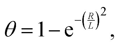 | (2) |
 | (3) |
To describe the time dependence of the coverage and perimeter (Fig. 2c), we need to relate the base size of Ge islands R to time t. This requires knowledge of the growth kinetics of individual Ge islands in the general case.37,38 In our MOVPE growth, this process can be simplified because the mean height of the Ge film (H) is linear in time for all t (Fig. 2c inset). The mean height (H) of the Ge layer equals θh, with h = αR as the mean height of Ge islands (including the merged islands) and α = h/R is the aspect ratio. Using the linear relationship
| θαR = v2D(t − t0), | (4) |
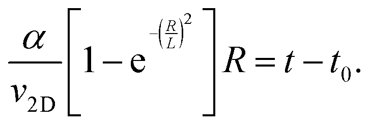 | (5) |
We now explain the growth kinetics of the Ge islands presented in Fig. 2c using the KJMA model. The lines in Fig. 2c show the fits to the data obtained from eqn (2), (3), and (5) with the parameters given in Table 1, which describe the observed morphological evolution of the Ge films. According to the data, the coverage of the Ge film increases, and the perimeter decreases significantly faster when we use AsH3 during the surface pretreatment step. On the other hand, the measured density of separated Ge islands in the pre-coalescence stage is higher without AsH3, corresponding to a larger maximum perimeter of the islands. Thus, we can conclude that the introduction of AsH3 in the surface pretreatment step reduces Ge nucleation and enhances Ge lateral growth with respect to its vertical growth, leading to a faster formation of a continuous Ge film inside the trenches.
| Surface pretreatment step | 2D growth rate v2D (nm s−1) | Nucleation time t0 (s) | Aspect ratio (α) | Separation between islands L (nm) | Maximum surface density N (μm−2) |
|---|---|---|---|---|---|
| With AsH3 | 0.745 | 2.8 | 0.8 | 13.5 | 1370 |
| Without AsH3 | 0.745 | 1.6 | 1.65 | 10.5 | 2268 |
The KJMA model also gives insights into the aspect ratio (α) and nucleation time (t0) for the Ge islands as a function of the surface pretreatment step (Table 1). For the surface pretreatment condition without AsH3, the nucleation of the 3D Ge islands occurs after t0 = 1.6 s, and the nuclei have an aspect ratio of 1.65. The presence of AsH3 during the surface pretreatment step delays the nucleation of 3D islands to t0 = 2.8 s and results in islands with a smaller aspect ratio, α = 0.8. The fitting values of the separation L yield higher maximum surface densities of Ge islands (calculated for the square base of Ge islands at c = 2) compared to the measured values after 5 s growth as shown in Table 1. Two reasons may cause this. First, the measured island densities at t = 5 s may not correspond to their maximum values. Second, the assumed instantaneous nucleation is an approximation, even if the nucleation stage is short compared to the total time of film growth.37
We attribute the differences in the nucleation density and the growth kinetics of Ge islands to the chemical nature of the Si (001) surface. According to ref. 39 and 40, introducing AsH3 during the surface pretreatment step serves two purposes. Firstly, at the annealing temperature of 820 °C used in this study, it ensures deoxidation of the silicon substrate. The H+ species produced by the dissociation of AsH3,41 remove carbon and oxygen from the Si surface.42,43 This is believed to happen through a surface reaction that results in volatile species such as CH4 and H2O.44 Secondly, As atoms passivate Si dangling bonds, providing a stable As-terminated Si surface for the growth of Ge.45,46 Under these conditions, Ge growth on the Si (001) surface follows the typical Stanski–Krastanov (SK) growth mode, where Ge islands are formed by the spontaneous transformation of an initially formed 2D wetting layer of Ge.47 The measured island surface density of 5 × 1010 cm−2 is within the range of values commonly reported for the SK growth of Ge on the Si (001) surface.48,49 In contrast, when AsH3 is omitted, we expect the presence of patches of residual oxide on the Si surface. This can be due to re-oxidation of the surface after the HF etch.50 The presence of an oxide drastically alters the growth mode. The growth of Ge on an oxidized Si surface follows the Volmer–Weber (VW) growth mode with the direct nucleation of a 3D island at the voids present in the SiO2 layer, without forming a wetting layer.51–53 It is interesting to note that Ge islands obtained on a Si surface covered with a thin oxide layer (0.5 nm to 1.2 nm thick) typically feature a very high nucleation density (2 × 1012 cm−2)51–53 and an aspect ratio close to 1.6 similar to the values observed in this study,53 which supports our claim. Based on this, we conclude that the calculated delay in the nucleation of the 3D island after the surface pre-treatment with AsH3 can be related to the formation of the wetting layer during the SK growth.
The presence of a residual oxide between the Ge islands also explains the differences we observe in the growth kinetics of the Ge islands. The low surface energy of the SiO2 (γSiO2 ≈ 0.4 J m−2)54 compared with the surface energy of Ge (γGe ≈ 1.05 to 1.71 J m−2)55 and the Ge–SiO2 interfacial energy (γGe–SiO2 ≈ 1 J m−2),56 promotes the vertical growth of Ge islands on SiO2 surface to minimize the total surface free energy. On the other hand, the Ge islands obtained on an AsH3 treated Si surface follow the SK growth mode and form on a 2D wetting layer of Ge.47 Here, the islands can expand laterally over the wetting layer until they reach an equilibrium state dictated by the strain energy resulting from lattice mismatch.57–59 Therefore, the higher aspect ratio and the enhanced vertical growth rate of Ge island observed after the surface pretreatment step without AsH3 are coherent with the presence of a residual oxide layer on the Si surface.
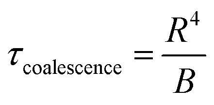
Having explained the differences in the growth kinetics of the Ge islands as a function of the surface pretreatment step, we now compare the morphology, chemical composition, and crystal quality of the Ge nanowires. Fig. 3 contains representative SEM and AFM images of the Ge nanostructures obtained as a function of the surface pretreatment step. The SEM images are acquired from an array of five parallel SiO2 trenches with a nominal width of 80 nm after 110 s of Ge growth. Fig. 3a shows the top view SEM image of an array of five continuous Ge nanowires obtained after the surface pretreatment step with AsH3. A representative AFM counterplot of a continuous nanowire is provided in Fig. 3c. Fig. 3b shows the top view SEM images of the discontinuous Ge islands inside the SiO2 trenches obtained after the surface pretreatment step without AsH3. A representative AFM counterplot of the discontinuous Ge islands is provided in Fig. 3d. The observed trend is consistent for Ge nanowires obtained from SiO2 trenches of varying nominal width (Fig. S4, ESI†). Both the SEM and AFM images indicate that the surface pretreatment step directly influences the continuity of SAE Ge nanowires. Ge nanowires with dimensions defined by the substrate patterning step are obtained only after the surface pretreatment step with AsH3 (Fig. 3a and c). By contrast, the omission of AsH3 (Fig. 3b and d) during the surface pretreatment step results in discontinuous Ge islands inside the trenches. The observed differences in the coalescence process are explained using Nicholas and Mullikan's model.60,61 A schematic illustration of our understanding of the coalescence process is provided in Fig. 3e. The coalescence of two crystalline islands into one larger island occurs by the surface diffusion of atoms caused by differences in the radius of curvature.61 The neck region formed at the point of impingement between two nearby islands gets preferentially filled by atoms diffusing down from the top surface of the islands.62 According to this description, the coalescence time between two impinging islands is quantitatively given by eqn (6), where R is the radius of the smaller island in the coalescing pair, and B is the coalescence strength.62,63
 | (6) |
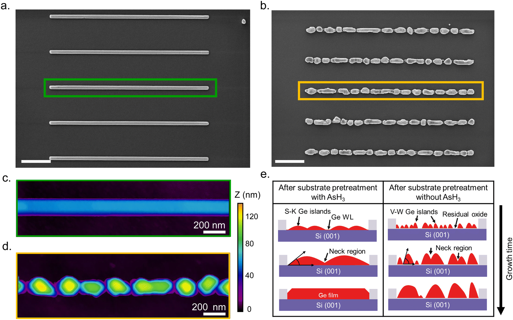 | ||
| Fig. 3 Effect of surface pretreatment condition on the continuity of Ge nanowires. (a) Top view SEM image of continuous Ge nanowires obtained after the surface pretreatment step with AsH3. (b) Top view SEM image of discontinuous Ge islands obtained after the surface pretreatment step without AsH3. The SEM images are acquired from an array of five SiO2 trenches with a nominal width of 80 nm after 110 s of growth. (c) AFM counterplot acquired from the continuous nanowire located at the center of the array shown in (a). (d) AFM counterplot acquired from the discontinuous Ge islands located at the center of the array shown in (b). (e) Schematic illustration of the coalescence process of the Ge islands as a function of the surface pretreatment condition. The scale bar shown in (a) and (b) indicates 1 μm. | ||
Once the neck region has been filled by the coalescence of islands, surface energy minimization brings the newly formed island to an equilibrium shape.62,63 The presence of an oxide layer on the Si surface after the surface pretreatment step without AsH3 influences the equilibrium shape and favors the formation of islands with high aspect ratios (α). As a result, the islands evolve into a more compact shape, as observed in Fig. 1b. Finally, the size of the islands (R) becomes prohibitively large for island coalescence to occur, and all the subsequent deposition of the atoms will feed the island growth, forming interconnected islands without coalescence as observed in Fig. 3b and d.
To evaluate the chemical composition of the nanowires, we prepared cross-sectional cuts perpendicular to the growth direction of the nanowires shown in Fig. 2 and examined them using a STEM. Further details on sample preparation for STEM are provided in the ESI.† The low magnification HAADF STEM images shown in Fig. 4a and b provide an overview of the cross-sections of five different nanowires obtained after surface pretreatment with and without AsH3, respectively. The cross-sections of the nanowires were analyzed by scanning transmission electron microscopy with energy dispersive X-ray spectroscopy (STEM-EDX) to quantitatively evaluate the elemental composition and distribution in the nanowires. The results of the STEM-EDX elemental mapping are shown in Fig. 4c and d. STEM-EDX elemental mapping profiles of individual elements are provided in the ESI† (Fig. S7 and S8). For the surface pretreatment condition with AsH3 (Fig. 4c), the chemical analysis by STEM-EDX confirms the Ge-rich composition of the nanowire and reveals the sharpness of the interface with the Si substrate. The EDX line scan profile taken along the nanowire-substrate interface shows a diffused interface with a slight migration of Si into the Ge up to a distance of 5 nm from the interface. The observed diffuse interface could also be due to the roughness of the Si surface created during the substrate fabrication (Fig. S3, ESI†). Qualitatively, we were also able to observe traces of As atoms within the Ge nanowires in the individual EDX composition map of As (Fig. S7, ESI†). However, we were not able to quantify them in the EDX line scans (Fig. 4c) or by collecting spectra from different points (Fig. S7, ESI†). From this, we can conclude that the arsenic doping in the Ge nanowires is minimal and within the detection limit of the STEM-EDX technique used in this study. In contrast, the Ge nanowires obtained after the surface pretreatment without AsH3 showed the presence of oxygen at the Ge/Si interface (Fig. 4c). The oxide layer was observed in all nanowire cross-sections analyzed in this study (Fig. S8, ESI†). Further details on the quality of the interfaces are described in the following sections.
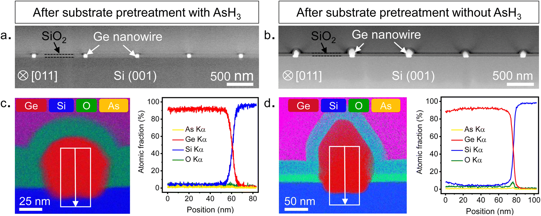 | ||
| Fig. 4 Compositional assessment of the Ge nanowires. HAADF-STEM micrograph of a cross-section cut made perpendicular to the in-plane orientation of five parallel nanowires obtained after surface pretreatment with AsH3 (a) and without AsH3 (b), respectively. (c) and (d) show the chemical composition of the Ge nanowires. (c) STEM-EDX elemental mapping showing the elemental distribution in Ge nanowires obtained after surface pretreatment with AsH3. The accompanying EDX line scan profile reveals the sharpness interface between the Ge nanowire and the Si substrate. (d) STEM-EDX elemental mapping showing the elemental distribution in Ge nanowires obtained after surface pretreatment without AsH3. The EDX line scan profile shows the presence of an oxide layer at the Ge nanowire/Si substrate interface. | ||
To assess the crystal quality, we analyzed the nanowire cross-sections presented in Fig. 4 using aberration-corrected STEM. Fig. 5 presents a comparison between the Ge nanowires obtained after the surface pretreatment step with and without AsH3 in terms of the cross-sectional morphology (a) and (e), strain distribution (b) and (f), and nanowire–substrate interface (c) and (g). When AsH3 is included in the surface pretreatment, nanowires exhibit uniform height and cross-sectional morphology, as depicted in Fig. 4a. We show an atomic resolution HAADF STEM image of a representative nanowire cross-section in Fig. 5a. The dotted lines in Fig. 5a indicate the cross-sectional morphology of the nanowire and are defined by facets belonging to the {110}, {111}, {001}, and {113} families, as in our previous work.4 We also observe a small amount of lateral growth along the [1−10] and [−110] directions above the oxide mask. Geometric phase analysis (GPA) of the nanowire cross-section (Fig. 5b) reveals plastic relaxation of the lattice mismatch by creating a periodic array of the misfit dislocation at the Ge/Si interface. In the present case, it seems that all strain is relaxed through plastic relaxation, with no presence of induced plane rotation at the lateral basis of the nanowire (elastic relaxation), as commonly observed in other nanowire systems.20,64,65 The magnified image of the Ge/Si interface in Fig. 5c shows a diffused interface indicative of the alloying between Si and Ge. In contrast, skipping AsH3 during the surface pretreatment step results in Ge islands with non-uniform height and cross-sectional morphology as observed in the HAADF STEM images (Fig. 4b and 5e). GPA analysis of the nanowire cross-section (Fig. 5f) shows the presence of stacking faults in addition to misfit dislocations. Finally, the magnified image of the Ge/Si interface presented in Fig. 5g shows patches of amorphous interfacial layer (white arrows). The Ge nanowire maintains an epitaxial relationship with the substrate but contains twin boundaries and stacking faults.
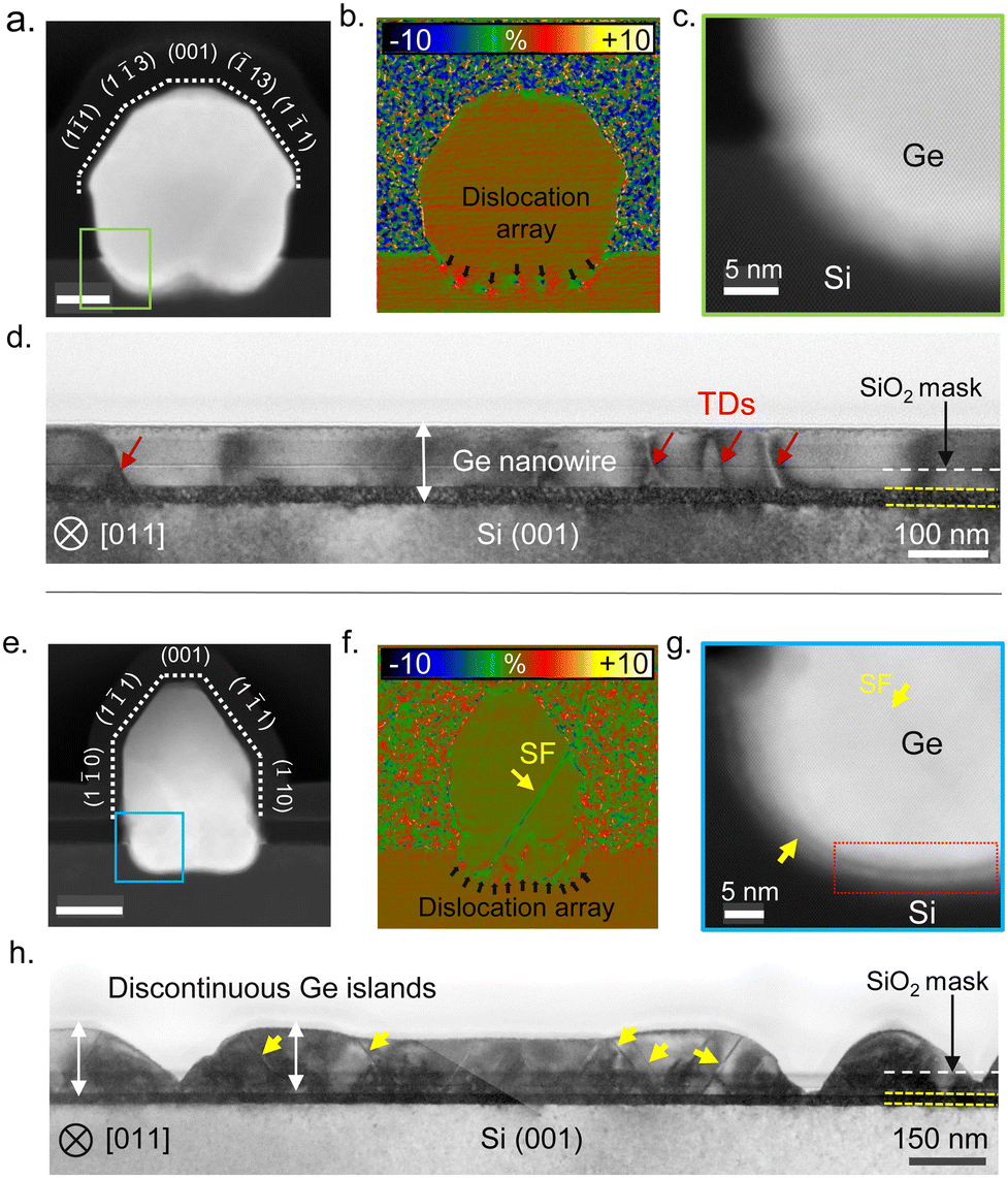 | ||
| Fig. 5 (a)–(d) Present cross-sectional morphology and crystal quality of the Ge nanowires obtained after the surface pretreatment condition with AsH3. (a) Atomic-resolution HAADF-STEM micrograph of a nanowire cross-section cut made perpendicular to the in-plane orientation. (b) GPA strain analysis map of the cross-section presented in panel (a), displaying mean plane rotation in the {111} plane. (c) Atomic-resolution HAADF-STEM image of the region marked in green in panel (a), revealing the presence of a diffused interface between the Ge nanowire and the Si substrate. (d) Bright-field TEM image of a cross-section cut made parallel to the in-plane orientation of the nanowire. The yellow dotted lines represent the moiré pattern, marking the interface between the Ge nanowire and the Si substrate. (e)–(h) Present the cross-sectional morphology and crystal quality of the Ge nanowires obtained after the surface pretreatment condition without AsH3. (e) Atomic-resolution HAADF-STEM micrograph of a nanowire cross-section cut made perpendicular to the in-plane orientation. (f) GPA strain analysis map of the cross-section presented in panel (e), indicating mean plane rotation in the {111} plane. (g) Atomic resolution HAADF STEM image of the region marked in blue in panel (e), revealing the presence of an interfacial amorphous layer (red box) at the interface between the Ge nanowire and the Si substrate. (h) Bright-field TEM image of a cross-section cut made parallel to the in-plane orientation of the nanowire. | ||
We further investigate the crystal quality along the length of the nanowire by preparing cross-sectional cuts parallel to the in-plane orientation of the nanowire. Fig. 5d and h show the bright field TEM image of cross-section cuts made parallel to the in-plane orientation of Ge nanowire obtained after surface pretreatment with and without AsH3, respectively. Although the nanowire growth occurs by the nucleation and coalescence of Ge islands, Ge nanowires obtained after the surface pretreatment step with AsH3 exhibited excellent crystal quality with few threading dislocations (red arrows in Fig. 5d). The contrast variation observed along the cross section in Fig. 5d originates from a strain developed during the coalescence of islands.66,67 Notably, the crystal quality that we observe in the present work is improved with respect to our previous work, where nanowire growth was carried out at 700 °C and the surface pretreatment step was performed at a lower temperature of 780 °C.4 We attribute the improvement in the crystal quality to the optimization of the surface pretreatment step and alloying of the interface due to a higher growth temperature. In contrast, skipping AsH3 during the surface pretreatment results in discontinuous Ge islands with a high density of twins and stacking faults as seen in Fig. 5e and h. Most defects start at the interface between the Ge islands and Si and extend into the upper part. The absence of extended planar defects in Ge nanowire samples grown after the surface pretreatment with AsH3 (Fig. 5a and d) suggests the residual oxide layer causes their nucleation. Ge islands nucleating on voids in the SiO2 layers can have a translation or tilt mismatch between adjacent islands. The coalescence of islands with translation mismatch generates stacking faults and twins in the Ge layer. In addition, the stress resulting from the thermal expansion mismatch between Ge and SiO2, or during the impingement of islands with a high aspect ratio, can also induce deformation twins in these structures.66
4. Conclusion
In summary, we investigate the selective area epitaxy of horizontal Ge nanowires on Si (001) substrates using MOVPE and demonstrate the impact of the use of AsH3 in the surface pretreatment step on the nanowire growth and crystal quality. The SAE of Ge nanowires proceeds by the nucleation and coalescence of Ge islands, and the introduction of AsH3 during the surface pretreatment step modifies the nucleation kinetics and coalescence process of the Ge islands. Using the KJMA crystallization model for the 2D projection of Ge islands, we model the coalescence process of Ge islands to understand the differences in nucleation and growth kinetics. Our results indicate that the epitaxy of Ge islands on the Si surface after the surface pretreatment step using AsH3 follows the Stanski–Krastanov growth mode. In contrast, skipping the AsH3 during the surface pre-treatment step results in the Volmer–Weber growth of Ge islands. We also show that using AsH3 during the surface pretreatment step enhances the lateral growth of the Ge islands, leading to a faster formation of continuous Ge film inside the trenches. Skipping AsH3 during the surface pretreatment step results in discontinuous Ge islands for the same growth time. We attribute the observed difference in the nucleation and growth to the differences in the chemical nature of the Si surface. The presence of AsH3 during the surface pretreatment step ensures the complete removal of native oxide of silicon and provides a clean As-terminated Si (001) surface for Ge epitaxy. Finally, Ge islands grown on the Si surface after the surface pretreatment step without AsH3 show the presence of a high density of planar defects (stacking faults and twins). On the contrary, planar defects are minimal on Ge nanowire grown with the AsH3 surface pretreatment. In this respect, this work demonstrates the importance of a thorough understanding of the chemical nature of the Si (001) surface and their control through in situ surface pretreatment to optimize the crystal quality of the SAE Ge nanowires.Author contributions
S. P. R. was responsible for substrate fabrication, nanowire growth and morphological characterization, BF-TEM analysis, STEM EDX compositional maps, and the fabrication of hall bar devices for electrical characterisation. J. R. conducted all the AFM measurements and performed data analysis. V. G. D. handled the KJMA modeling of the coalescence process and wrote the corresponding sections of the manuscript. S. M. and J. A. conducted aberration-corrected scanning transmission electron microscopy studies. A. R. contributed to optimizing the Ge nanowire growth recipes and maintaining the MOCVD facility. A. M. was responsible for fabricating the top gated device and conducting magneto transport measurements. A. F. i. M. was responsible for funding acquisition, resources, and project supervision. S. P. R. conceptualized the work and wrote the manuscript together with A. F. i. M., with inputs from V. G. D. and J. A. All authors commented on the work and approved the final version of the manuscript.Conflicts of interest
There are no conflicts to declare.Acknowledgements
This work was supported as a part of NCCR SPIN, a National Centre of Competence (or Excellence) in Research, funded by the Swiss National Science Foundation (Grant no. 51NF40-180604). Authors also thank access and training in the cleanroom and electron microscopy facilities of EPFL, CMI, and CIME. VGD acknowledges funding from the Swiss National Science Foundation (Grant ID IZSEZ0-213059) and St. Petersburg State University (Grant ID 94033852). ICN2 acknowledges funding from Generalit at de Catalunya 2021SGR00457. This study is part of the Advanced Materials program and was supported by MCIN with funding from European Union Next GenerationEU (PRTR-C17.I1) and by Generalit at de Catalunya. We acknowledge support from CSIC Interdisciplinary Thematic Platform (PTI+) on Quantum Technologies (PTI-QTEP+). All the authors thank Prof. Andreas Mortensen, Prof. Klaus Ensslin, and Prof. Thomas Ihn for their feedback on the manuscript and discussions. S. P. R. gratefully thanks Shelly Ben-David and Anja Tiede for helping with editing the manuscript. Authors acknowledge the use of instrumentation as well as the technical advice provided by the National Facility ELECMI ICTS, node “Laboratorio de Microscopías Avanzadas” at the University of Zaragoza. This research is part of the CSIC program for the Spanish Recovery, Transformation, and Resilience Plan funded by the Recovery and Resilience Facility of the European Union, established by the Regulation (EU) 2020/2094. The authors acknowledge the use of instrumentation as well as the technical advice provided by the Joint Electron Microscopy Center at ALBA (JEMCA). ICN2 acknowledges funding from Grant IU16-014206 (METCAM-FIB) funded by the European Union through the European Regional Development Fund (ERDF), with the support of the Ministry of Research and Universities, Generalitat de Catalunya. ICN2 is a founding member of e-DREAM.68References
- X. Yuan, D. Pan, Y. Zhou, X. Zhang, K. Peng, B. Zhao, M. Deng, J. He, H. H. Tan and C. Jagadish, Selective area epitaxy of III–V nanostructure arrays and networks: Growth, applications, and future directions, Appl. Phys. Rev., 2021, 8, 021302 CAS.
- L. Guniat, P. Caroff and A. Fontcuberta i Morral, Vapor phase growth of semiconductor nanowires: key developments and open questions, Chem. Rev., 2019, 119, 8958–8971 CrossRef CAS PubMed.
- M. Friedl, et al., Template-Assisted Scalable Nanowire Networks, Nano Lett., 2018, 18, 2666–2671 CrossRef CAS PubMed.
- S. P. Ramanandan, P. Tomić, N. P. Morgan, A. Giunto, A. Rudra, K. Ensslin, T. Ihn and A. Fontcuberta i Morral, Coherent Hole Transport in Selective Area Grown Ge Nanowire Networks, Nano Lett., 2022, 22, 4269–4275 CrossRef CAS PubMed.
- N. Morgan, V. G. Dubrovskii, A.-K. Stief, D. Dede, M. Sanglé-Ferriére, A. Rudra, V. Piazza and A. Fontcuberta i Morral, From Layer-by-Layer Growth to Nanoridge Formation: Selective Area Epitaxy of GaAs by MOVPE, Cryst. Growth Des., 2023, 23, 5083–5092 CrossRef CAS PubMed.
- P. Aseev, et al., Selectivity Map for Molecular Beam Epitaxy of Advanced III–V Quantum Nanowire Networks, Nano Lett., 2019, 19, 218–227 CrossRef CAS PubMed.
- J. Jung, S. G. Schellingerhout, M. F. Ritter, S. C. ten Kate, O. A. van der Molen, S. de Loijer, M. A. Verheijen, H. Riel, F. Nichele and E. P. Bakkers, Selective Area Growth of PbTe Nanowire Networks on InP, Adv. Funct. Mater., 2022, 32, 2208974 CrossRef CAS.
- A. R. Wagner and S. W. Ellis, Vapor-liquid-solid mechanism of single crystal growth, Appl. Phys. Lett., 1964, 4, 89–90 CrossRef.
- P. McIntyre, i Morral, A. F. Semiconductor nanowires: to grow or not to grow?, Mater. Today Nano, 2020, 9, 100058 CrossRef.
- W. Lu, J. Xiang, B. P. Timko, Y. Wu and C. M. Lieber, One-dimensional hole gas in germanium/silicon nanowire heterostructures, Proc. Natl. Acad. Sci. U. S. A., 2005, 102, 10046–10051 CrossRef CAS PubMed.
- S. Conesa-Boj, A. Li, S. Koelling, M. Brauns, J. Ridderbos, T. T. Nguyen, M. A. Verheijen, P. M. Koenraad, F. A. Zwanenburg and E. P. Bakkers, Boosting hole mobility in coherently strained [110]-oriented Ge–Si core–shell nanowires, Nano Lett., 2017, 17, 2259–2264 CrossRef CAS PubMed.
- M. A. Khan, Y. Ishikawa, I. Kita, A. Tani, H. Yano, T. Fuyuki and M. Konagai, Investigation of crystallinity and planar defects in the Si nanowires grown by vapor– liquid–solid mode using indium catalyst for solar cell applications, Jpn. J. Appl. Phys., 2015, 55, 01AE03 CrossRef.
- M. A. Khan, Y. Ishikawa, I. Kita, K. Fukunaga, T. Fuyuki and M. Konagai, Control of verticality and (111) orientation of In-catalyzed silicon nanowires grown in the vapour– liquid–solid mode for nanoscale device applications, J. Mater. Chem. C, 2015, 3, 11577–11580 RSC.
- L. Güniat, P. Caroff and A. Fontcuberta, Vapor Phase Growth of Semiconductor Nanowires: Key Developments and Open Questions, Chem. Rev., 2019, 119, 8958–8971 CrossRef PubMed.
- P. Staudinger, K. E. Moselund and H. Schmid, Exploring the Size Limitations of Wurtzite III–V Film Growth, Nano Lett., 2020, 20, 686–693 CrossRef CAS PubMed.
- A. Hager, L. Güniat, N. Morgan, S. P. Ramanandan, A. Rudra, V. Piazza, A. Fontcuberta i Morral and D. Dede, The implementation of thermal and UV nanoimprint lithography for selective area epitaxy, Nanotechnology, 2023, 34, 445301 CrossRef PubMed.
- J. Jung, S. G. Schellingerhout, M. F. Ritter, S. C. ten Kate, O. A. van der Molen, S. de Loijer, M. A. Verheijen, H. Riel, F. Nichele and E. P. Bakkers, Selective AreaGrowth of PbTe Nanowire Networks on InP, Adv. Funct. Mater., 2022, 32, 2208974 CrossRef CAS.
- S. Escobar Steinvall, E. Z. Stutz, R. Paul, M. Zamani, J.-B. Leran, M. Dimitrievska and A. Fontcuberta i Morral, Nanoscale Growth Initiation as a Pathway to Improve the Earth-Abundant Absorber Zinc Phosphide, ACS Appl. Energy Mater., 2022, 5, 5298–5306 CrossRef CAS PubMed.
- M. Friedl, K. Cerveny, C. Huang, D. Dede, M. Samani, M. O. Hill, N. Morgan, W. Kim, L. Güniat, J. Segura-Ruiz, L. J. Lauhon, D. M. Zumbühl and A. Fontcuberta i Morral, Remote Doping of Scalable Nanowire Branches, Nano Lett., 2020, 20, 3577–3584 CrossRef CAS PubMed.
- D. V. Beznasyuk, S. Martí-Sánchez, J.-H. Kang, R. Tanta, M. Rajpalke, T. C. V. Stankevič, A. W. Christensen, M. C. Spadaro, R. Bergamaschini, N. N. Maka, C. E. N. Petersen, D. J. Carrad, T. S. Jespersen, J. Arbiol and P. Krogstrup, Doubling the mobility of InAs/InGaAs selective area grown nanowires, Phys. Rev. Mater., 2022, 6, 034602 CrossRef CAS.
- G. Scappucci, C. Kloeffel, F. A. Zwanenburg, D. Loss, M. Myronov, J.-J. Zhang, S. D. Franceschi, G. Katsaros and M. Veldhorst, The germanium quantum information route. Nature Reviews, Materials, 2020, 6, 926–943 Search PubMed.
- C. Kloeffel, M. Trif and D. Loss, Strong spin-orbit interaction and helical hole states in Ge/Si nanowires, Phys. Rev. B: Condens. Matter Mater. Phys., 2011, 84, 195314 CrossRef.
- A. P. Higginbotham, F. Kuemmeth, T. W. Larsen, M. Fitzpatrick, J. Yao, H. Yan, C. M. Lieber and C. M. Marcus, Antilocalization of Coulomb Blockade in a Ge/Si Nanowire, Phys. Rev. Lett., 2014, 112, 216806 CrossRef.
- S. Bosco and D. Loss, Fully Tunable Hyperfine Interactions of Hole Spin Qubits in Si and Ge Quantum Dots, Phys. Rev. Lett., 2021, 127, 190501 CrossRef CAS PubMed.
- J. S. Lee, S. Choi, M. Pendharkar, D. J. Pennachio, B. Markman, M. Seas, S. Koelling, M. A. Verheijen, L. Casparis and K. D. Petersson, et al., Selective-area chemical beam epitaxy of in-plane InAs one-dimensional channels grown on InP (001), InP (111) B, and InP (011) surfaces, Phys. Rev. Mater., 2019, 3, 084606 CrossRef CAS.
- R. L. Op het Veld, D. Xu, V. Schaller, M. A. Verheijen, S. M. Peters, J. Jung, C. Tong, Q. Wang, M. W. de Moor and B. Hesselmann, et al., In-plane selective area InSb–Al nanowire quantum networks, Commun. Phys., 2020, 3, 59 CrossRef CAS.
- D. Dede, F. Glas, V. Piazza, N. Morgan, M. Friedl, L. Güniat, E. N. Dayi, A. Balgarkashi, V. G. Dubrovskii and A. F. i Morral, Selective area epitaxy of GaAs: The unintuitive role of feature size and pitch, Nanotechnology, 2022, 33, 485604 CrossRef PubMed.
- S. E. Steinvall, E. Z. Stutz, R. Paul, M. Zamani, N. Y. Dzade, V. Piazza, M. Friedl, V. De Mestral, J.-B. Leran and R. R. Zamani, et al., Towards defect-free thin films of the earth-abundant absorber zinc phosphide by nanopatterning, Nanoscale Adv., 2021, 3, 326–332 RSC.
- M. C. Spadaro, S. E. Steinvall, N. Y. Dzade, S. Martí-Sánchez, P. Torres-Vila, E. Z. Stutz, M. Zamani, R. Paul, J.-B. Leran and A. F. i Morral, et al., Rotated domains in selective area epitaxy grown Zn 3 P 2: formation mechanism and functionality, Nanoscale, 2021, 13, 18441–18450 RSC.
- J. Jung, S. G. Schellingerhout, O. A. Van Der Molen, W. H. Peeters, M. A. Verheijen and E. P. Bakkers, Single-crystalline PbTe film growth through reorientation, Phys. Rev. Mater., 2023, 7, 023401 CrossRef CAS.
- O. Skibitzki, G. Capellini, Y. Yamamoto, P. Zaumseil, M. A. Schubert, T. Schroeder, A. Ballabio, R. Bergamaschini, M. Salvalaglio, L. Miglio and F. Montalenti, Reduced-Pressure Chemical Vapor Deposition Growth of Isolated Ge Crystalsand Suspended Layers on Micrometric Si Pillars, ACS Appl. Mater. Interfaces, 2016, 8, 26374–26380 CrossRef CAS PubMed.
- A. Kolmogorov, On the Statistical Theory of Metal Crystallization, Izv. Akad. Nauk SSSR, Ser. Math., 1937, 1, 335–360 Search PubMed ; Computes density of fairly general Johnson-Mehl crystals and the probability that a point is not in a crystal yet.
- W. A. Johnson and R. F. Mehl, Reaction kinetics in processes of nucleation and growth, Trans. Am. Inst. Min. Metall. Eng., 1939, 135, 416–442 Search PubMed.
- M. Avrami, Kinetics of phase change. I general theory, J. Chem. Phys., 1939, 7, 1103–1112 CrossRef CAS.
- V. G. Dubrovskii, Nucleation theory and growth of nanostructures, Springer, Berlin, 2016 Search PubMed.
- V. Dubrovskii, G. Cirlin, Y. Musikhin, Y. Samsonenko, A. Tonkikh, N. Polyakov, V. Egorov, A. Tsatsul’nikov, N. Krizhanovskaya, V. Ustinov and P. Werner, Effect of growth kinetics on the structural and optical properties of quantum dot ensembles, J. Cryst. Growth, 2004, 267, 47–59 CrossRef CAS.
- V. G. Dubrovskii, Nucleation and growth of adsorbed layer self-consistent approach based on Kolmogoroff-Avrami model, Phys. Status Solidi B, 1992, 171, 345–356 CrossRef CAS.
- V. G. Dubrovskii, N. V. Sibirev and A. S. Sokolovskii, Kinetic broadening of size distribution in terms of natural versus invariant variables, Phys. Rev. E, 2021, 103, 012112 CrossRef CAS PubMed.
- I. Miccoli, P. Prete and N. Lovergine, Shape, Size Evolution, and Nucleation Mechanisms of GaAs Nanoislands Grown on (111)Si by Low-Temperature Metal–Organic VaporPhase Epitaxy, Cryst. Growth Des., 2019, 19, 5523–5530 CrossRef CAS.
- T. E. Saenz, W. E. McMahon, A. G. Norman, C. L. Perkins, J. D. Zimmerman and E. L. Warren, High-Temperature Nucleation of GaP on V-Grooved Si, Cryst. Growth Des., 2020, 20, 6745–6751 CrossRef CAS.
- A. Jordan and A. Robertson, Equilibrium gas-phase composition and thermodynamic properties including subhydrides in the pyrolysis of AsH3 and PH3, J. Cryst. Grow., 1993, 128, 488–493 CrossRef CAS.
- T. Hannappel, W. McMahon and J. Olson, An RDS, LEED, and STM study of MOCVDprepared Si (1 0 0) surfaces, J. Cryst. Grow., 2004, 272, 24–29 CrossRef CAS.
- T. Bork, W. McMahon, J. Olson and T. Hannappel, Surface science studies including low-temperature RDS on MOCVD-prepared, As-terminated Si (1 0 0) surfaces, J. Cryst. Grow., 2007, 298, 54–58 CrossRef CAS.
- A. Navarro de Mesa, E. García-Tabarés Valdivieso, Q. M. Ramasse, P. Caño, I. ReyStolle and B. Galiana Blanco, Advanced transmission electron microscopy investigation of defect formation in movpe-growth of gap on silicon using arsenic initial coverage, Appl. Surf. Sci., 2023, 610, 155578 CrossRef.
- O. Supplie, O. Romanyuk, C. Koppka, M. Steidl, A. Nägelein, A. Paszuk, L. Winterfeld, A. Dobrich, P. Kleinschmidt and E. Runge, et al., Metalorganic vapor phase epitaxy of III–V-on-silicon: Experiment and theory, Prog. Cryst. Growth Charact. Mater., 2018, 64, 103–132 CrossRef CAS.
- T. E. Saenz, W. E. McMahon, A. G. Norman, C. L. Perkins, J. D. Zimmerman and E. L. Warren, High-temperature nucleation of GaP on v-grooved si, Cryst. Growth Des., 2020, 20, 6745–6751 CrossRef CAS.
- L. Pan, K.-K. Lew, J. M. Redwing and E. C. Dickey, StranskiKrastanow Growth of Germanium on Silicon Nanowires, Nano Lett., 2005, 5, 1081–1085 CrossRef CAS PubMed.
- A. Rastelli, M. Kummer and H. von Känel, Reversible Shape Evolution of Ge Islands on Si(001), Phys. Rev. Lett., 2001, 87, 256101 CrossRef CAS PubMed.
- F. M. Ross, J. Tersoff and R. M. Tromp, Coarsening of Self-Assembled Ge Quantum Dots on Si(001), Phys. Rev. Lett., 1998, 80, 984–987 CrossRef CAS.
- I. Yoon, C. Yi, T. Kim, A. S. Brown and A. Seabaugh, Effect of surface pretreatment and substrate orientation on the characteristics of InAs quantum dots on Si and SiO2 substrates, J. Vac. Sci. Technol., B: Microelectron. Nanometer Struct.–Process., Meas., Phenom., 2007, 25, 945–947 CrossRef CAS.
- A. A. Shklyaev and M. Ichikawa, Extremely dense arrays of germanium and silicon nanostructures, Phys.-Usp., 2008, 51, 133 CrossRef CAS.
- K. A. Lozovoy, A. P. Kokhanenko, V. V. Dirko, N. Y. Akimenko and A. V. Voitsekhovskii, Evolution of epitaxial quantum dots formed by Volmer–Weber Growth Mechanism, Cryst. Growth Des., 2019, 19, 7015–7021 CrossRef CAS.
- Q. Li, B. Pattada, S. R. J. Brueck, S. Hersee and S. M. Han, Morphological evolution and strain relaxation of Ge islands grown on chemically oxidized Si(100) by molecular-beam epitaxy, J. Appl. Phys., 2005, 98, 073504 CrossRef.
- C. Y. Chuang, Q. Li, D. Leonhardt, S. M. Han and T. Sinno, Atomistic analysis of Ge on amorphous SiO2 using an empirical interatomic potential, Surf. Sci., 2013, 609, 221–229 CrossRef CAS.
- A. A. Stekolnikov, J. Furthmüller and F. Bechstedt, Absolute surface energies of group-IV semiconductors: Dependence on orientation and reconstruction, Phys. Rev. B: Condens. Matter Mater. Phys., 2002, 65, 115318 CrossRef.
- J. Du and P. Kroll, Electronic structure and interfacial properties of Ge nanoclusters embedded in amorphous silica, J. Non-Cryst. Solids, 2010, 356, 2448–2453 CrossRef CAS 12th International Conference on the Physics of Non-Crystalline Solids (PNCS 12).
- H. Hu, H. Gao and F. Liu, Theory of directed nucleation of strained islands on patterned substrates, Phys. Rev. Lett., 2008, 101, 216102 CrossRef PubMed.
- F. Gao, J.-H. Wang, H. Watzinger, H. Hu, M. J. Rančić, J.-Y. Zhang, T. Wang, Y. Yao, G.-L. Wang and J. Kukučka, et al., Site-controlled uniform Ge/Si hut wires with electrically tunable spin–orbit coupling, Adv. Mater., 2020, 32, 1906523 CrossRef CAS PubMed.
- J. Tersoff and R. Tromp, Shape transition in growth of strained islands: Spontaneous formation of quantum wires, Phys. Rev. Lett., 1993, 70, 2782 CrossRef CAS PubMed.
- F. Nichols, Coalescence of two spheres by surface diffusion, J. Appl. Phys., 1966, 37, 2805–2808 CrossRef CAS.
- F. Nichols and W. Mullins, Morphological changes of a surface of revolution due tocapillarity-induced surface diffusion, J. Appl. Phys., 1965, 36, 1826–1835 CrossRef.
- X. Yu, P. M. Duxbury, G. Jeffers and M. A. Dubson, Coalescence and percolation in thin metal films, Phys. Rev. B: Condens. Matter Mater. Phys., 1991, 44, 13163–13166 CrossRef PubMed.
- B. Lü, V. Elofsson, E. Münger and K. Sarakinos, Dynamic competition between island growth and coalescence in metal-on-insulator deposition, Appl. Phys. Lett., 2014, 105 Search PubMed.
- S. Martí-Sánchez, M. Botifoll, E. Oksenberg, C. Koch, C. Borja, M. C. Spadaro, V. Di Giulio, Q. Ramasse, F. J. García de Abajo and E. Joselevich, et al., Subnanometer mapping of strain-induced band structure variations in planar nanowire core-shell heterostructures, Nat. Commun., 2022, 13, 4089 CrossRef PubMed.
- F. Krizek, J. E. Sestoft, P. Aseev, S. Marti-Sanchez, S. Vaitiek˙enas, L. Casparis, S. A. Khan, Y. Liu, T. Stankevič and A. M. Whiticar, et al., Field effect enhancement in buffered quantum nanowire networks, Phys. Rev. Mater., 2018, 2, 093401 CrossRef CAS.
- B. W. Sheldon, K. H. A. Lau and A. Rajamani, Intrinsic stress, island coalescence, and su face roughness during the growth of polycrystalline films, J. Appl. Phys., 2001, 90, 5097–5103 CrossRef CAS.
- J. Jung, S. G. Schellingerhout, O. A. H. van der Molen, W. H. J. Peeters, M. A. Verheijen and E. P. A. M. Bakkers, Single-crystalline PbTe film growth through reorientation, Phys. Rev. Mater., 2023, 7, 023401 CrossRef CAS.
- R. Ciancio, R. E. Dunin-Borkowski, E. Snoeck, M. Kociak, R. Holmestad, J. Verbeeck, A. I. Kirkland, G. Kothleitner and J. Arbiol, e-DREAM: the European Distributed Research Infrastructure for Advanced Electron Microscopy, Microsc. Microanal., 2022, 28, 2900–2902 CrossRef.
Footnote |
| † Electronic supplementary information (ESI) available: It contains details of the substrate preparation, selective area epitaxy (SAE) of germanium, atomic force microscopy (AFM) study and data processing, effect of surface pretreatment on the continuity of the Ge nanostructures, transmission electron microscopy (TEM) studies, chemical composition analysis, electrical characterization of the nanowires and atomic resolution HAADF-STEM imaging. See DOI: https://doi.org/10.1039/d3nh00573a |
| This journal is © The Royal Society of Chemistry 2024 |