
Integrating ultraviolet sensing and memory functions in gallium nitride-based optoelectronic devices†
Kuan-Chang
Chang
 a,
Xibei
Feng
a,
Xinqing
Duan
a,
Huangbai
Liu
a,
Yanxin
Liu
a,
Zehui
Peng
a,
Xinnan
Lin
*b and
Lei
Li
*a
a,
Xibei
Feng
a,
Xinqing
Duan
a,
Huangbai
Liu
a,
Yanxin
Liu
a,
Zehui
Peng
a,
Xinnan
Lin
*b and
Lei
Li
*a
aSchool of Electronic and Computer Engineering, Peking University Shenzhen Graduate School, Shenzhen, 518055, China. E-mail: lilei@pkusz.edu.cn
bAnhui Engineering Research Center of Vehicle Display Integrated Systems, Joint Discipline Key Laboratory of Touch Display Materials and Devices, School of Integrated Circuits, Anhui Polytechnic University, Wuhu 241000, China. E-mail: xnlin@mail.ahpu.edu.cn
First published on 16th April 2024
Abstract
Optoelectronic devices present a promising avenue for emulating the human visual system. However, existing devices struggle to maintain optical image information after removing external stimuli, preventing the integration of image perception and memory. The development of optoelectronic memory devices offers a feasible solution to bridge this gap. Simultaneously, the artificial vision for perceiving and storing ultraviolet (UV) images is particularly important because UV light carries information imperceptible to the naked eye. This study introduces a multi-level UV optoelectronic memory based on gallium nitride (GaN), seamlessly integrating UV sensing and memory functions within a single device. The embedded SiO2 side-gates around source and drain regions effectively extend the lifetime of photo-generated carriers, enabling dual-mode storage of UV signals in terms of threshold voltage and ON-state current. The optoelectronic memory demonstrates excellent robustness with the retention time exceeding 4 × 10⁴ s and programming/erasing cycles surpassing 1 × 10⁵. Adjusting the gate voltage achieves five distinct storage states, each characterized by excellent retention, and efficiently modulates erasure times for rapid erasure. Furthermore, the integration of the GaN optoelectronic memory array successfully captures and stably stores specific UV images for over 7 days. The study marks a significant stride in optoelectronic memories, showcasing their potential in applications requiring prolonged retention.
New conceptsWe present an optoelectronic device based on gallium nitride (GaN) that uniquely integrates ultraviolet (UV) signal sensing with memory capabilities. This new concept diverges significantly from existing research, which has predominantly focused on optoelectronic devices that sense optical signals without the concurrent capability to store these signals effectively. Our GaN-based device, enhanced by a novel side-gate structure formed through the embedding of SiO2 barriers at the source and drain electrodes, facilitates the effective storage of photogenerated carriers. This allows the conversion of perceived UV signals into electrical signals (threshold voltage and ON-state current), which are then stored within the device. Our work offers multiple new insights: it demonstrates the feasibility of multi-stage storage of UV signals, meeting the demand for multi-bit signal storage and paving the way for more complex signal processing. Additionally, our demonstration of storing specific UV images using GaN optoelectronic memory arrays highlights their potential in advanced imaging applications. This integration of sensing and memory in a single GaN-based device marks a major stride in UV photoelectric applications, underscoring the potential of multifunctional integrated optoelectronic memories. These are crucial for the development of GaN optoelectronic integrated circuits and represent a substantial leap forward in artificial vision systems. |
Introduction
The human visual system has inspired the advancement of optoelectronic sensing and storage devices.1,2 Visual perception and memory involve the processes of learning and memorizing optical information, such as images and text. Various optical image sensing devices, including pixel image sensor arrays, have emerged as favorable choices to emulate biological vision functions.3–5 However, current optical image sensing devices primarily focus on real-time perception and recognition of specific images, with limited efforts on storing and recalling detected image information.6–8 In the human visual system, effective storage of image signals is as vital as perception, constituting a key factor in the efficient utilization of optical signals. Therefore, the lack of memory ability of image sensors is a critical flaw that needs overcoming. To address this gap, the combination of optoelectronic sensors and memory components to simultaneously detect and store optical information has become a feasible choice for emulating the biological visual system.9–11 In comparison to discrete optoelectronic sensing and memory devices, advanced optoelectronic storage devices, integrating optoelectronic sensing and memory functions, overcome signal transmission bottlenecks and substantially improve the efficiency of information perception, processing, and storage.Generally, daily visual information perceived by the human eye comes from visible light. Nevertheless, ultraviolet (UV) signals, invisible to the naked eye, carry specific details and phenomena beyond the visible range.12–14 In nature, certain insects and mammals possess tetrachromatic vision, enabling them to perceive UV images and aiding in their hunting, survival, and environmental adaptation.15–18 In human society, the importance of UV signals has been recognized across various domains, including fire detection, military defense, and societal security.19–21 Nonetheless, the invisibility of UV signals complicates their capture, storage, and interpretation and utilization. The development of UV detection and storage devices has therefore become a crucial task, conducive to enhancing human cognitive understanding of the world and playing a pivotal role in critical sectors such as security, national defense, and environmental preservation.22–24 Among numerous electronic materials and devices, gallium nitride (GaN) stands out as an excellent candidate for UV sensing due to its direct and wide-bandgap (3.4 eV) and physical properties,25–28 demonstrating favorable UV absorption windows and physical and chemical stability under complex and extreme conditions (such as space, high-pressure, and high-temperature environments).29,30 Choosing GaN as the material for manufacturing optoelectronic devices can achieve specific response to UV signals and avoid interference from visible light signals, thereby achieving filter-free sensing and storage of UV light signals. In addition, compared with emerging materials such as gallium oxide, GaN's process flow is relatively mature and its cost is lower. Since GaN has been used in business and its commercialization potential and application fields are wider. Moreover, optoelectronic devices based on GaN materials can be compatible with existing mature semiconductor processes, facilitating the integration of multiple devices on a single chip, thus enabling the realization of a complete GaN-based integrated circuit. Recent years have witnessed widespread attention on GaN-based UV detection technologies,28–30 including p–i–n structured UV photodetectors developed using GaN nanowires and asymmetric structures composed of Au/nanoporous GaN/graphene vertical junctions,31,32 specifically tailored for visible-blind UV detection. Despite the significant progress in UV signal detection using GaN-based UV detectors, there remains a deficiency in the ability to store and recall the detected UV image information once external UV signals are removed. This limitation is attributed to the high carrier recombination rate within GaN materials, which hinders optoelectronic devices from achieving long-term storage of optical signals. Therefore, effective UV signal storage remains a critical aspect for the recognition and efficient utilization of UV signals, presenting a continuous challenge.
What's more, with the explosive growth of contemporary data volume and the increasing demand for digital computation, traditional data memory devices are approaching their limits. Consequently, memories that can achieve multi-level memory states have become a new direction of current research. Extensive research using various materials and structures has demonstrated the potential for achieving multi-level storage states.33–36 The multi-level memory states can also be integrated with neuromorphic computing functionalities. Therefore, the effort to develop multi-level memory states is vital for handling the growing data volumes and achieving more complex functionalities in single devices.
Here, we present a multi-level UV optoelectronic memory based on GaN. An embedded silicon dioxide side-gate structure is introduced to address the issue of short storage time of photo-generated carriers in GaN when exposed to UV radiation. This structure restricts the direct connection between the two-dimensional electron gas in the channel and the source–drain electrodes, thereby achieving the storage of photo-generated carriers. The proposed scheme has endowed the device with stable non-volatile multi-level storage capabilities while perceiving UV signals. Notably, the device exhibits threshold voltage and ON-state current storage modes, with highly reliable information storage, maintaining a retention time exceeding 4 × 10⁴ s and endurance more than 1 × 10⁵ cycles. Through the modulation of gate voltage, the device not only realizes stable five-level storage but also efficiently adjusts the erasure speed for rapid erasure. Furthermore, specific UV images are successfully captured and stored by integrating a GaN storage pixel array. Remarkably, the array maintains the excellent storage characteristics of the captured images even after 7 days. This study also provides a cross-validation of the working mechanisms of GaN optoelectronic storage devices in terms of electrical characterization, materials, and low-frequency noise analysis. The successful implementation of simultaneous UV sensing and memory within a single GaN device not only provides an insight into the storage of GaN UV sensing information, but also contributes to the advancement of GaN-based optoelectronic integrated circuits.
Results and discussion
Fig. 1a shows the three-dimensional optical microscopy images of the GaN-based UV optoelectronic memory array and devices. Fig. 1b provides both the schematic diagram of the GaN UV optoelectronic memory and its top view image captured through scanning electron microscopy (SEM). The memory device was programmed by irradiating UV light on the gate region. The polarization effect of the AlGaN/AlN/GaN heterostructure enhanced the two-dimensional electron gas (2DEG) formation in the GaN channel.37,38 Notably, the SiO2 side-gates embedded at the source and drain electrodes are highlighted using the red boxes in the SEM image of Fig. 1b. Fig. 1c displays the layers in the gate region, where Al/Ti/TiN metals were utilized as the gate electrode. The dielectric layer, Si3N4, and the heterojunction layer, AlGaN/AlN, featuring a 24.5 nm thick AlGaN layer and an approximately 0.7 nm thick AlN layer, demonstrate the excellent uniformity of the device fabrication process. Energy dispersive X-ray spectroscopy (EDS) characterization in the gate region also provides direct evidence for the characterization of the heterojunction and dielectric layer structures, as shown in Fig. S1 (ESI†). Taking the drain electrode side as an example, the TEM image in Fig. 1d clearly shows the SiO2 side-gate structure embedded near the drain electrode. In Fig. S2 (ESI†), X-ray photoelectron spectroscopy (XPS) characterization was conducted to analyze the elemental composition, which further confirmed the successful preparation of the heterojunction, dielectric layer, and side-gate structure. The basic transfer characteristics (IDS–VGS) and output characteristics (IDS–VDS) of the prepared devices were measured, as shown in Fig. S3a and b (ESI†). The mobility of the device was extracted from the transfer characteristics in Fig. S3b (ESI†) to be 286.4 cm2 V−1 s−1.39 Fig. S3c (ESI†) depicts the excellent performance and ultra-low gate leakage (∼10 fA) exhibited by the GaN device.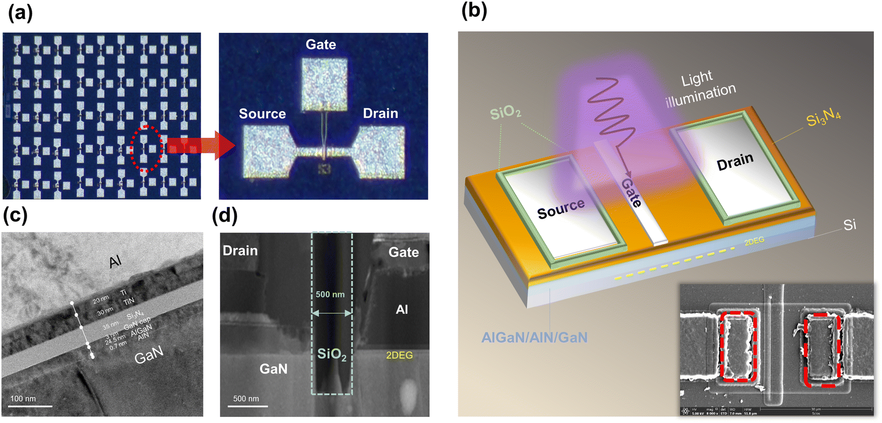 | ||
| Fig. 1 (a) 3D optical microscopy images of the GaN ultraviolet optoelectronic memory device. (b) The schematic diagram of the GaN ultraviolet optoelectronic memory and its SEM top view image. (c) The TEM image shows the cross-sectional multi-layer structure in the gate region. (d) The TEM image of the gate-drain area displays the structure of embedded side-gate SiO2. | ||
The UV optoelectronic memory function has been developed on the GaN devices. Fig. 2a illustrates the schematic diagram of the UV programming process, wherein the device is exposed to a UV light pulse with a wavelength of 340 nm (duration: 5 s, intensity: 32 mW cm−2) while experiencing a negative gate pulse (−20 V). Fig. 2b compares the device's transfer characteristics before and after UV irradiation. IDS was measured by sweeping VGS from −20 V to 0 V while maintaining VDS at 0.1 V. After UV irradiation, the device exhibited a significant negative shift in the threshold voltage and an increase in the ON-state current signifying the successful conversion of the UV signal into electrical signals stored in the device. Fig. S4 (ESI†) also shows that the hysteresis window of the device will not be significantly affected by UV light programming. Compared with the threshold voltage shift caused by photogenerated hole storage, the change amount in hysteresis is still minor and negligible. This means that hysteresis does not significantly affect the interpretation of the threshold voltage storage effect. Fig. S5a (ESI†) demonstrates the device's responses to light across broader wavelengths (770–340 nm), showcasing its substantial storage response exclusively to UV signals (340 nm) and highlighting the specific UV sensitivity of the GaN optoelectronic memory. Fig. S5b (ESI†) shows the influence of UV irradiation duration on the programming speed and memory state, illustrating the device's effective information storage capability even in brief periods.
 | ||
| Fig. 2 (a) Schematic representation of the UV programming process of the GaN optoelectronic memory. (b) The transfer curves of the GaN memory at VDS = 0.1 V before and after UV programming. (c) A single program–readout–erase cycle of the GaN optoelectronic memory at programming voltage VGS = −20 V. (d)–(f) Schematic illustration of the gate energy band of the GaN optoelectronic memory during programming, readout and erasing processes. | ||
Fig. 2c comprehensively depicts the dynamic behavior of the GaN optoelectronic memory in a single cycle, including programming (P), readout (R), and erasure (E) processes. The mechanisms of these three processes are illustrated in Fig. 2d–f. Due to the direct and wide bandgap characteristics of GaN, photogenerated electron–hole pairs were produced in the AlGaN/GaN heterostructure under UV pulse (340 nm) illumination with a power density of 32 mW cm−2. During the programming process, the photogenerated carrier pairs were separated under the influence of the gate electric field. The electrons transitioned to the conduction band while holes tunneled through AlN and accumulated in the AlGaN barrier layer, as shown in Fig. 2d. The threshold voltage after programming was determined by measuring the transfer characteristics and the storage ON-state current after programming was read out at 0 V gate voltage under dark conditions, as shown in Fig. 2e. The transitioned photogenerated holes were stably stored in the AlGaN barrier layer, forming a stable positive charge storage effect and thus resulting in a shielding effect on the negative gate voltage. As a result, a larger negative gate voltage was required to turn on the device, causing the threshold voltage to drift from −13.4 V to −15.1 V. Simultaneously, due to the presence of SiO2 side-gates, the photogenerated electrons could not rapidly escape from the source–drain electrodes after entering the conduction band but were stored in the 2DEG of the channel. When the gate voltage was switched to 0 V, a sharp rise of current was observed, stabilizing at around 56 μA, indicating the nonvolatile properties of the GaN optoelectronic memory (Fig. 2c).
We further explored the transition behavior of photogenerated carriers in the device through 1/f noise measurements. Fig. S6a and b (ESI†) display the normalized power spectral density of the device noise before and after UV programming, respectively. The main noise source in the subthreshold region is the movement of carriers in and out of AlN defects in the channel. Calculations revealed that the defect density of AlN increased from 4.56 × 1019 cm−3 eV−1 to 5.51 × 1019 cm−3 eV−1 after programming.40 This indicates that the photogenerated holes indeed tunneled through the AlN layer during UV programming of the memory, creating new defects in the AlN layer.
To erase the storage state, a positive gate voltage was applied to the GaN memory to remove the charges stored in the AlGaN barrier layer and GaN channel. Fig. S7 (ESI†) shows that the larger gate voltage can cause the faster erasure operation. Fig. 2f shows that when the positive gate electric field was strong, the photogenerated holes stored in the AlGaN barrier layer returned to the GaN channel and recombined with the channel electrons. Therefore, the erase operation in Fig. 2b was achieved by applying a positive gate voltage (VGS = 12 V) for 2 s, leading to the local positive charges in the AlGaN barrier layer to disappear and the threshold voltage returned to the initial value of −13.4 V. The electrons stored in the channel were also recombined, and the ON-state current returned to 52 μA. Experimental results demonstrate that the device can achieve fast erase switching of memory states.
To evaluate the reliability of the GaN optoelectronic memory in practical applications, the retention and endurance characteristics of the two storage modes, represented by the memory window through shifts in the threshold voltage (ΔVTH) and ON-state current (ΔIDS), were tested under undisturbed dark conditions. Fig. 3a displays the variation of device's transfer characteristics over time with the sweep conditions ranging from −20 V to 0 V, revealing its capability to effectively maintain the altered transfer characteristics after UV programming, indicative of robust retention performance. Fig. 3b and c show the threshold voltage and ON-state current from the transfer characteristics at a fixed interval of 1 × 10³ s to determine the memory windows. Despite a slight initial narrowing of the memory windows, both the threshold voltage and ON-state current windows remain stable and reliable within the time range of 4 × 10⁴ s. To explore the storage retention capability of the GaN optoelectronic memory, the fitting results of the retention curves for ΔVTH and ΔIDS present double-exponential decay, as shown in Fig. S8 (ESI†). According to the fitting results, ΔVTH is projected to stabilize at 1.661 V and ΔIDS will be stable at 0.678 μA (S6 and Fig. S8, ESI†), achieving long-term stable storage. Moreover, the device exhibited stable storage characteristics under varying temperature conditions of 85 °C and 125 °C, indicating the excellent data retention properties of the GaN optoelectronic memory (Fig. S9, ESI†). Continuous programming and erasing operations were performed on the device to explore its endurance. Fig. 3d records the device's transfer characteristics after 10, 100, 1000, 10![[thin space (1/6-em)]](https://www.rsc.org/images/entities/char_2009.gif) 000 and 100000 programming and erasure cycles. Memory windows, exhibited by ΔVTH and ΔIDS, were extracted from the transfer curves to evaluate the endurance of the memory device. Fig. 3e shows that the memory window of ΔVTH after 1 × 10⁵ cycles experiences a slight decrease but still maintains a reliable storage state of over 70%. Fig. 3f also exhibits that window of ΔIDS still maintains over 60% of the memory window after 1 × 10⁵ cycles. These experimental results clearly indicate that the GaN optoelectronic memory exhibits an ultralong retention time and robust endurance, demonstrating its potential for practical applications.
000 and 100000 programming and erasure cycles. Memory windows, exhibited by ΔVTH and ΔIDS, were extracted from the transfer curves to evaluate the endurance of the memory device. Fig. 3e shows that the memory window of ΔVTH after 1 × 10⁵ cycles experiences a slight decrease but still maintains a reliable storage state of over 70%. Fig. 3f also exhibits that window of ΔIDS still maintains over 60% of the memory window after 1 × 10⁵ cycles. These experimental results clearly indicate that the GaN optoelectronic memory exhibits an ultralong retention time and robust endurance, demonstrating its potential for practical applications.
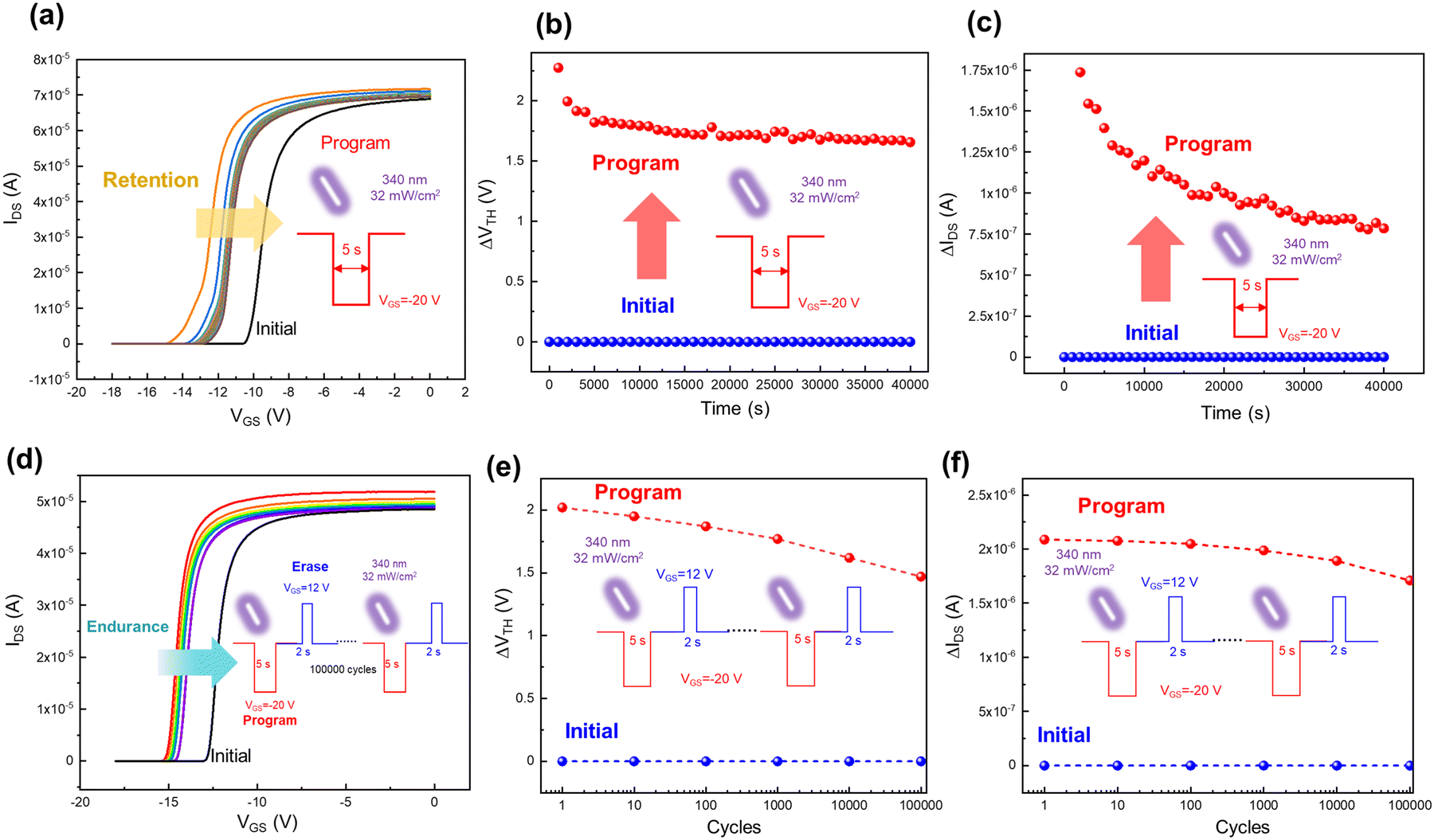 | ||
| Fig. 3 (a) The transfer characteristics changing with time after UV programming. (b) and (c) Retention characteristics of the memory windows represented by ΔVTH and ΔIDS, respectively. (d) The device's transfer characteristic curves after 100000 programming and erasing cycles. (e) and (f) Endurance characteristics demonstrated by the memory windows of ΔVTH and ΔIDS. | ||
The GaN optoelectronic memory developed in this study not only possesses stable and reliable storage capabilities but also exhibits multi-level storage capabilities, as depicted in Fig. 4a. As the programming voltage (VGS) increases, the stored threshold voltage shows a stepwise increase and the memory window of ΔVTH gradually expands. Fig. 4b shows the threshold voltage memory window (ΔVTH) extracted from the transfer curves. When the programming gate voltage VGS ranges from −11 V to −29 V, ΔVTH gradually increases from 1.1 V to 4.05 V, achieving five distinct storage states. Higher negative programming gate voltages facilitate the efficient separation of photogenerated electron–hole pairs, allowing a higher concentration of positive charges in the AlGaN barrier layer. This phenomenon resulted in a further negative drift of the device's threshold voltage, enabling multi-level storage. To confirm the reliability of multi-level storage in the optoelectronic memory, the threshold voltage was extracted at fixed intervals of 1 × 10³ s to determine the threshold voltage storage window, as indicated in Fig. 4c. Fig. S10 (ESI†) also shows the retention characteristics of the device's transfer curves for five storage states. The results demonstrate the remarkably stable maintenance of multi-level storage states in the GaN optoelectronic memory within a time range exceeding 4 × 10⁴ s. These findings underscore the exceptional long-term storage capability for multi-level data in the GaN optoelectronic memory, demonstrating its substantial potential for practical applications, especially in image capture scenarios that demand requiring the recording of extensive data.
 | ||
| Fig. 4 (a) Transfer characteristics indicating the multi-level memory with different programming VGS, ranging from −11 V to −29 V. (b) The five storage states of the threshold voltage modulated by VGS. (c) The retention characteristics of five storage states. | ||
Fig. 5a illustrates the sensing and memorization of visible information in the human visual system, where the visible information from the external world is perceived by the retina, followed by delivery of the visual data to the visual cortex in the brain for memory.41,42 In order to simulate this complex biological process, we designed and constructed a 5 × 9 GaN optoelectronic memory array for real-time image detection and memory of UV signals, as shown in Fig. 5b. Firstly, we tested the transfer characteristics of each device in the array to obtain the initial threshold voltage. Then we placed the mask of the “EYE” image above the device array and irradiated the exposed devices with ultraviolet light. The programming process was conducted for 5 seconds under 340 nm light with an intensity of 32 mW cm−2. During this process, the gate voltage of −20 V was applied to each device. After the illumination ended, we removed the gate voltage and tested the post-exposure transfer characteristics of the devices in order to obtain the post-exposure threshold voltage. The GaN memory devices programmed by UV signals showed a significant negative threshold voltage drift, reaching the maximum drift of approximately −3 V. In contrast, the threshold voltage of the GaN devices not exposed to UV signals remained stable. The entire array successfully sensed the image “EYE”, as shown in Fig. 5b. Subsequently, we tested the transfer characteristics of each device again after 1 day and 7 days, extracting their threshold voltages to observe the memory characteristics of the array for ultraviolet signals. Although the stored “EYE” image showed slight decay after one day, it remained clear and discernible. Remarkably, even after 7 days, the “EYE” image continued to exhibit clear storage states. This demonstrates that the GaN-based optoelectronic memory array realizes the function of sensing and storing UV signals, so that UV images can be captured and effectively stored for a long time. The integration of sensing and memory greatly simplifies the complexity of the artificial vision system. This is not only crucial for the development of future artificial vision systems, but also has important implications in the application of UV signals in fields such as communications, military identification, and others. This achievement also highlights the great potential of GaN-based optoelectronic integrated circuits in technology and applications.
 | ||
| Fig. 5 (a) The human visual system for visible information sensing and memorization. (b) The schematic diagram of the 5 × 9 GaN optoelectronic memory array and the optical image “EYE” sensing and memorization over 7 days. | ||
Conclusions
In summary, this work has demonstrated a multi-level UV optoelectronic memory utilizing GaN, emulating the human visual memory process by integrating the detection and memory of UV images. The embedded SiO2 side-gates around the source–drain region of GaN devices effectively suppress the rapid dissipation of photogenerated electron–hole pairs in GaN under UV light illumination. This allows their separation under gate electric field, resulting in significant and stable changes in threshold voltage and ON-state current and the establishment of two stable memory windows. This unique mechanism enables the GaN optoelectronic memory to effectively store UV signals in dual modes, exhibiting excellent retention (exceeding 4 × 10⁴ seconds) and endurance characteristics (more than 1 × 10⁵ programming and reading cycles). By adjusting the gate-controlled voltage (VGS) during programming, the device exhibited multi-level storage capabilities, demonstrating its potential for extensive data storage applications. Moreover, the proposed GaN-based UV optoelectronic multi-level memory integrates UV signal detection and storage on a single device and the memory array constructed from this device is capable of efficiently detecting and storing UV images, greatly simplifying the complexity of UV signal processing by artificial vision systems.Methods
Device fabrication
First, the epitaxial wafer was cleaned using deionized water, hydrofluoric acid solution, and standard cleaning solution SC-1 (a mixture of ammonia, hydrogen peroxide, and water) for removing surface impurities. Second, devices were subjected to dry etching for on-chip isolation, with an etching depth of approximately 300 nm. SiO2 was then deposited into the isolation trenches to block the interconnection of two-dimensional electron gas between devices. Third, source and drain electrode openings were etched by dry etching, followed by consecutive deposition of Ti/Al/Ti/TiN using physical vapor deposition (PVD). Source and drain electrodes were formed after photolithographic patterning. Similarly, gate electrode openings were etched by dry etching, followed by PVD deposition of TiN/Ti/Al. Gate electrodes were formed after photolithographic patterning. Fourth, the side gate openings were etched surrounding the source and drain electrodes by the dry etching process. Finally, SiO2 was filled in the side-gate openings, simultaneously completing the deposition of the protective dielectric layer.Materials characterization
XPS spectroscopy was applied to analyze the elemental composition and chemical bonds in the material. SEM and TEM were also applied to help with the microscopic characterization process to prove the existence of SiO2 side-gates embedded around source and drain electrodes.Optoelectrical measurements
All basic I–V electrical measurements were carried out with a Keysight 4200 semiconductor parameter analyzer. The 1/f noise measurement was measured using a 9812B and an Agilent 35670. The wavelength of UV pulse was measured using an Ocean USB4000 and an LS125 UV light meter with a UVA-X1 detector was used to confirm the intensity of UV pulse.
Author contributions
K. C. Chang, X. B. Feng and L. Li were responsible for the device fabrication, investigation, methodology and writing the original draft. L. Li and K. C. Chang conceived the idea, analyzed the data and wrote the paper. X. Q. Duan and H. B. Liu contributed to optical measurements. Y. X. Liu and Z. H. Peng conducted the material analysis. X. N. Lin helped with the device fabrication and contributed to the noise analysis. L. Li and X. N. Lin contributed to the project administration and funding acquisition. All authors have discussed the results and commented on the manuscript.Conflicts of interest
There are no conflicts to declare.Acknowledgements
This study was supported by the National Natural Science Foundation of China (no. 62204007 and 62074007), Shenzhen Municipal Scientific Program (no. JCYJ20220531093210023 and JCYJ20200109140610435), and the Start-up funding of Anhui Polytechnic University (2023YQQ003).References
- S. Hong, H. Cho, B. H. Kang, K. Park, D. Akinwande, H. J. Kim and S. Kim, Neuromorphic Active Pixel Image Sensor Array for Visual Memory, ACS Nano, 2021, 15(9), 15362–15370 CrossRef CAS PubMed.
- R. Desimone, Neural Mechanisms for Visual Memory and Their Role in Attention, Proc. Natl. Acad. Sci. U. S. A., 1996, 93, 13494–13499 CrossRef CAS PubMed.
- E. K. Vogel and M. G. Machizawa, Neural Activity Predicts Individual Differences in Visual Working Memory Capacity, Nature, 2004, 428, 748–751 CrossRef CAS PubMed.
- F. Sun, Q. Lu, L. Liu, L. Li, Y. Wang, M. Hao, Z. Cao, Z. Wang, S. Wang, T. Li and T. Zhang, Bioinspired Flexible, DualModulation Synaptic Transistors toward Artificial Visual Memory Systems, Adv. Mater. Technol., 2020, 5, 1–8 Search PubMed.
- Q. B. Zhu, B. Li, D. D. Yang, C. Liu, S. Feng, M. L. Chen, Y. Sun, Y. N. Tian, X. Su, X. M. Wang, S. Qiu, Q. W. Li, X. M. Li, H. B. Zeng, H. M. Cheng and D. M. Sun, A Flexible Ultrasensitive Optoelectronic Sensor Array for Neuromorphic Vision Systems, Nat. Commun., 2021, 12, 1–7 CrossRef PubMed.
- W. Deng, X. J. Zhang, L. M. Huang, X. Z. Xu, L. Wang, J. C. Wang, Q. X. Shang, S. T. Lee and J. S. Jie, Aligned Single-Crystalline Perovskite Microwire Arrays for High-Performance Flexible Image Sensors with Long-Term Stability, Adv. Mater., 2016, 28, 2201 CrossRef CAS PubMed.
- L. L. Gu, M. M. Tavakoli, D. Q. Zhang, Q. P. Zhang, A. Waleed, Y. Q. Xiao, K. H. Tsui, Y. J. Lin, L. Liao, J. N. Wang and Z. Y. Fan, 3D Arrays of 1024-Pixel Image Sensors based on Lead Halide Perovskite Nanowires, Adv. Mater., 2016, 28, 9713 CrossRef CAS PubMed.
- Y. L. Chu, X. H. Wu, J. J. Lu, D. P. Liu, J. Du, G. Q. Zhang and J. Huang, Photosensitive and Flexible Organic Field-Effect Transistors Based on Interface Trapping Effect and Their Application in 2D Imaging Array, Adv. Sci., 2016, 3, 1500435 CrossRef PubMed.
- Q. B. Zhu, B. Li, D. D. Yang, C. Liu, S. Feng, M. L. Chen, Y. Sun, Y. N. Tian, X. Su, X. M. Wang, S. Qiu, Q. W. Li, X. M. Li, H. B. Zeng, H. M. Cheng and D. M. Sun, A flexible ultrasensitive optoelectronic sensor array for neuromorphic vision systems, Nat. Commun., 2021, 12, 1798 CrossRef CAS PubMed.
- S. Wang, H. Chen, T. Liu, Y. Wei, G. Yao, Q. Lin, X. Han, C. Zhang and H. Huang, Retina-Inspired Organic Photonic Synapses for Selective Detection of SWIR Light, Angew. Chem., 2023, 135, e202213733 CrossRef.
- B. Pradhan, S. Das, J. Li, F. Chowdhury, J. Cherusseri, D. Pandey, D. Dev, A. Krishnaprasad, E. Barrios, A. Towers, A. Gesquiere, L. Tetard, T. Roy and J. Thomas, Ultrasensitive and ultrathin phototransistors and photonic synapses using perovskite quantum dots grown from graphene lattice, Sci. Adv., 2020, 6, eaay5225 CrossRef CAS PubMed.
- S. Chen, Z. Lou, D. Chen and G. Z. Shen, An Artificial Flexible Visual Memory System Based on an UV-Motivated Memristor, Adv. Mater., 2018, 30, 1705400 CrossRef PubMed.
- F. Zhou, Z. Zhou, J. Chen, T. H. Choy, J. Wang, N. Zhang, Z. Lin, S. Yu, J. Kang, H.-S. P. Wong and Y. Chai, Optoelectronic resistive random access memory for neuromorphic vision sensors, Nat. Nanotechnol., 2019, 14, 776–782 CrossRef CAS PubMed.
- G. Li, D. Xie, H. Zhong, Z. Zhang, X. Fu, Q. Zhou, Q. Li, H. Ni, J. Wang, E. Guo, M. He, C. Wang, G. Yang, K. Jin and G. Chen, Photo-induced non-volatile VO2 phase transition for neuromorphic ultraviolet sensors, Nat. Commun., 2022, 13, 1729 CrossRef CAS PubMed.
- F. Sun, Q. Lu, L. Liu, L. Li, Y. Wang, M. Hao, Z. Cao, Z. Wang, S. Wang, T. Li and T. Zhang, Bioinspired flexible, dual-modulation synaptic transistors toward artificial visual memory systems, Adv. Mater. Technol., 2019, 5, 1900888 CrossRef.
- T. W. Cronin and M. J. Bok, Photoreception and vision in the ultraviolet, J. Exp. Biol., 2016, 219, 2790–2801 CrossRef PubMed.
- A. Matsushita, F. Stewart, M. Ilić, P. Chen, D. Wakita, N. Miyazaki, K. Murata, M. Kinoshita, G. Belušič and K. Arikawa, Connectome of the lamina reveals the circuit for early color processing in the visual pathway of a butterfly, Curr. Biol., 2022, 32, 2291–2299 CrossRef CAS PubMed.
- Z. Zhang, X. Zhao, X. Zhang, X. Hou, X. Ma, S. Tang, Y. Zhang, G. Xu, Q. Liu and S. Long, In-sensor reservoir computing system for latent fingerprint recognition with deep ultraviolet photo-synapses and memristor array, Nat. Commun., 2022, 13, 6590 CrossRef CAS PubMed.
- M. Peng, Y. Liu, A. Yu, Y. Zhang, C. Liu, J. Liu, W. Wu, K. Zhang, X. Shi, J. Kou, J. Zhai and Z. L. Wang, Flexible Self-Powered GaN Ultraviolet Photoswitch with Piezo-Phototronic Effect Enhanced On/Off Ratio, ACS Nano, 2016, 10(1), 1572–1579 CrossRef CAS PubMed.
- P. Cheong, K. F. Chang, Y. H. Lai, S. K. Ho, I. K. Sou, K. W. Tam and A. ZigBee-Based Wireless Sensor, Network Node for Ultraviolet Detection of Flame, IEEE Trans. Ind. Electron., 2011, 58, 5271–5277 Search PubMed.
- J. Orphal, A critical review of the absorption cross-sections of O3 and NO2 in the ultraviolet and visible., J. Photochem. Photobiol., A, 2003, 157, 185–209 CrossRef CAS.
- H. Chen, K. Liu, L. Hu, A. A. Al-Ghamdi and X. Fang, New concept ultraviolet photodetectors, Mater. Today, 2015, 18, 493–502 CrossRef CAS.
- J. Chen, W. Ouyang, W. Yang, J. H. He and X. Fang, Recent Progress of Heterojunction Ultraviolet Photodetectors: Materials, Integrations, and Applications, Adv. Funct. Mater., 2020, 30, 1909909 CrossRef CAS.
- Q. Zhang, X. Li, Z. He, M. Xu, C. Jin and X. Zhou, 2D Semiconductors Towards High-Performance Ultraviolet Photodetection, J. Phys. D: Appl. Phys., 2019, 52, 303002 CrossRef CAS.
- G. J. Jeong, J. H. Lee, S. H. Han, W. Y. Jin, J. W. Kang and S. N. Lee, Silver nanowires for transparent conductive electrode to GaN-based light-emitting diodes, Appl. Phys. Lett., 2015, 106(3), 031118 CrossRef.
- S. Jung, K. R. Song, S. N. Lee and H. Kim, Wet chemical etching of semipolar GaN planes to obtain brighter and cost-competitive light emitters, Adv. Mater., 2013, 25, 4470–4476 CrossRef CAS PubMed.
- G. Wang, H. Lu, D. Chen, F. Ren, R. Zhang and Y. Zheng, High Quantum Efficiency GaN-Based p-i-n Ultraviolet Photodetectors Prepared on Patterned Sapphire Substrates, IEEE Photonics Technol. Lett., 2013, 25(7), 652–654 CAS.
- X. Zhang, B. Liu, Q. Liu, W. Yang, C. Xiong, J. Li and X. Jiang, Ultrasensitive and Highly Selective Photodetections of UV-A Rays Based on Individual Bicrystalline GaN Nanowire, ACS Appl. Mater. Interfaces, 2017, 9, 2669–2677 CrossRef CAS PubMed.
- H. R. Golgir, D. W. Li, K. Keramatnejad, Q. M. Zou, J. Xiao, F. Wang, L. Jiang, J. F. Silvain and Y. F. Lu, Fast Growth of GaN Epilayers via Laser-Assisted Metal−Organic Chemical Vapor Deposition for Ultraviolet Photodetector Applications, ACS Appl. Mater. Interfaces, 2017, 9, 21539–21547 CrossRef PubMed.
- T. Hu, L. Zhao, Y. Wang, H. Lin, S. Xie, Y. Hu, C. Liu, W. Zhu, Z. Wei, J. Liu and K. Wang, High-Sensitivity and Fast-Speed UV Photodetectors Based on Asymmetric Nanoporous-GaN/Graphene Vertical Junction, ACS Nano, 2023, 17(9), 8411–8419 CrossRef CAS PubMed.
- A. L. Bugallo, M. Tchernycheva, G. Jacopin, L. Rigutti, F. H. Julien, S. T. Chou, Y. T. Lin, P. H. Tseng and L. W. Tu, Visible-blind photodetector based on p-i-n junction GaN nanowire ensembles, Nanotechnology, 2010, 21, 315201 CrossRef PubMed.
- T. Hu, L. Zhao, Y. Wang, H. Lin, S. Xie, Y. Hu, C. Liu, W. Zhu, Z. Wei, J. Liu and K. Wang, High-Sensitivity and Fast-Speed UV Photodetectors Based on Asymmetric Nanoporous-GaN/Graphene Vertical Junction, ACS Nano, 2023, 17(9), 8411–8419 CrossRef CAS PubMed.
- M. Kumar, J. Park, J. Kim and H. Seo, Room-Temperature Quantum Diodes with Dynamic Memory for Neural Logic Operations, ACS Appl. Mater. Interfaces, 2023, 15(48), 56003–56013 CrossRef CAS PubMed.
- M. Kumar, S. I. Han, S. W. Lim and H. Seo, Hybrid Volatile/Nonvolatile Resistive Switching Memory in Ternary Metal Oxide Enabling Hopfield Neural Classification, ACS Appl. Electron. Mater., 2023, 5(2), 896–904 CrossRef CAS.
- M. Y. Chougale, M. U. Khan, J. Kim, C. M. Furqan, Q. M. Saqib, R. A. Shaukat, S. R. Patil, B. Mohammad, H.-S. Kwok and J. Bae, Highly Flexible and Asymmetric Hexagonal-Shaped Crystalline Structured Germanium Dioxide-Based Multistate Resistive Switching Memory Device for Data Storage and Neuromorphic Computing, Adv. Electron. Mater., 2022, 8, 2200332 CrossRef CAS.
- T. D. Dongale, S. S. Sutar, Y. D. Dange, A. C. Khot, S. S. Kundale, S. R. Patil, S. V. Patil, A. A. Patil, S. S. Khot, P. J. Patil, J. Bae, R. K. Kamat and T. Kim, Machine learning-assisted design guidelines and performance prediction of CMOS-compatible metal oxide-based resistive switching memory devices, Appl. Mater. Today, 2022, 29, 101650 CrossRef.
- I. P. Smorchkova, C. R. Elsass, J. P. Ibbetson, R. Vetury, B. Heying, P. Fini, E. Haus, S. P. DenBaars, J. S. Speck and U. K. Mishra, Polarization-induced charge and electron mobility in AlGaN/GaN heterostructures grown by plasma-assisted molecular-beam epitaxy, J. Appl. Phys., 1999, 86(8), 4520–4526 CrossRef CAS.
- L. Shen, S. Heikman, B. Moran, R. Coffie, N. Q. Zhang, D. Buttari, I. P. Smorchkova, S. Keller, S. P. DenBaars and U. K. Mishra, AlGaN/AlN/GaN high-power microwave HEMT, IEEE Electron Device Lett., 2001, 22(10), 457–459 CAS.
- K. C. Chang, X. B. Feng, H. B. Liu, K. Liu, X. N. Lin and L. Li, “Computational-fitting Method for Mobility Extraction in GaN HEMT”, RCS Adv., 2023, 13, 32694–32698 CAS.
- J. Brini, G. Ghibaudo, G. Kamarinos and O. Roux-dit-Buisson, Scaling down and low-frequency noise in MOSFET's Are the RTS's the ultimate components of the 1/f noise?, AIP Conf. Proc., 1992, 282(1), 31–48 CrossRef.
- X. Hou, C. Liu, Y. Ding, L. Liu, S. Wang and P. Zhou, A LogicMemory Transistor with the Integration of Visible Information Sensing-Memory-Processing, Adv. Sci., 2020, 7, 2002072 CrossRef CAS PubMed.
- M. Karbalaei Akbari, J. Hu, F. Verpoort, H. Lu and S. Zhuiykov, Nanoscale All-Oxide-Heterostructured Bio-Inspired Optoresponsive Nociceptor, Nano-Micro Lett., 2020, 12, 83 CrossRef PubMed.
Footnote |
| † Electronic supplementary information (ESI) available. See DOI: https://doi.org/10.1039/d3nh00560g |
| This journal is © The Royal Society of Chemistry 2024 |