
 Open Access Article
 This Open Access Article is licensed under a Creative Commons Attribution-Non Commercial 3.0 Unported Licence
Atomic-level imaging of beam-sensitive COFs and MOFs by low-dose electron microscopy
Zhen
Zhan
a,
Yuxin
Liu
a,
Weizhen
Wang
a,
Guangyu
Du
a,
Songhua
Cai
 *a and
Peng
Wang
*b
*a and
Peng
Wang
*b
aDepartment of Applied Physics, The Hong Kong Polytechnic University, Kowloon 999077, Hong Kong SAR, China. E-mail: songhua.cai@polyu.edu.hk
bDepartment of Physics, University of Warwick, CV4 7AL, Coventry, UK. E-mail: peng.wang.3@warwick.ac.uk
First published on 21st March 2024
Abstract
Electron microscopy, an important technique that allows for the precise determination of structural information with high spatiotemporal resolution, has become indispensable in unravelling the complex relationships between material structure and properties ranging from mesoscale morphology to atomic arrangement. However, beam-sensitive materials, particularly those comprising organic components such as metal–organic frameworks (MOFs) and covalent organic frameworks (COFs), would suffer catastrophic damage from the high energy electrons, hindering the determination of atomic structures. A low-dose approach has arisen as a possible solution to this problem based on the integration of advancements in several aspects: electron optical system, detector, image processing, and specimen preservation. This article summarizes the transmission electron microscopy characterization of MOFs and COFs, including local structures, host–guest interactions, and interfaces at the atomic level. Revolutions in advanced direct electron detectors, algorithms in image acquisition and processing, and emerging methodology for high quality low-dose imaging are also reviewed. Finally, perspectives on the future development of electron microscopy methodology with the support of computer science are presented.
1. Introduction
Chemistry and materials science have long been focused on understanding molecular and atomic structure/orientation to design novel materials with desired physicochemical properties. Crystalline molecules with a regular arrangement and long-range order serve as an ideal target for elucidating the relationships between inherent structures and properties, thus providing a controllable and quantifiable array. Inorganic crystals have been the primary focus of crystal research for several decades, owing to their exceptional physicochemical stability and processability.1,2 However, this stability can limit structural design flexibility due to relatively fixed-mode binding. In contrast, organic building blocks exhibit greater designability and diversity, endowing organic-containing composites with exceptional structural flexibility.3 However, similar to the conflicts between diversity and stability, the controllability of precise multilevel structure from the molecular junctions to the condensed-matter structure may be exponential-growth as the active site increases, leading to the sluggish development of crystalline organic materials (COMs). The construction of primary and high-order alignment through the retention of inorganic building elements (metal ions or clusters) and their connection with organic linkages has been proposed. Originally referred to as coordination polymers, these structures are now commonly known as metal–organic frameworks (MOFs).4 The discovery of the crystallization of MOFs has prompted researchers to explore methods for synthesizing crystalline structures from solely organic building blocks through covalent bonds, instead of coordination interactions. Then, the pioneering covalent organic frameworks (COFs), which combine covalent and noncovalent interactions, were first reported by Yaghi and colleagues5 in 2005, with their development occurring over the past decade. The extraordinary expansion of MOFs and COFs can be attributed to the versatile organic linkers. As shown in Fig. 1, over the past decade, more than 100![[thin space (1/6-em)]](https://www.rsc.org/images/entities/char_2009.gif) 000 articles about MOFs have been reported, and COFs, despite their later inception, have also experienced exponential growth. In addition to their diverse construction units, MOFs and COFs exhibit several intriguing characteristics, such as exceptional chemical stability, intrinsic porosity, and the potential for post-modification or hybridization. These attractive features have numerous applications in fields such as gas adsorption and separation,6,7 heterogeneous catalysis,8,9 and energy storage and conversion.10,11
000 articles about MOFs have been reported, and COFs, despite their later inception, have also experienced exponential growth. In addition to their diverse construction units, MOFs and COFs exhibit several intriguing characteristics, such as exceptional chemical stability, intrinsic porosity, and the potential for post-modification or hybridization. These attractive features have numerous applications in fields such as gas adsorption and separation,6,7 heterogeneous catalysis,8,9 and energy storage and conversion.10,11
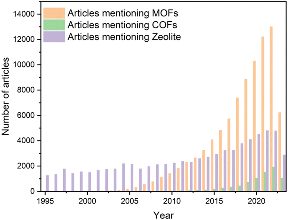 | ||
| Fig. 1 Papers mentioning “metal organic framework”, “covalent organic framework” and “zeolite” in the title, the abstract or the keyword, as searched in Web of Science in Aug 2023. | ||
The topology diagram of MOFs and COFs is guided by the judicious selection of organic building blocks, resulting in a predesignable skeleton.12,13 Such a well-defined alignment facilitates the determination of the structure–property relationship, thereby enabling the design of specific functionalized materials. To gain a comprehensive understanding of their structure, numerous state-of-the-art techniques have been applied, ranging from the holistic to the localized and atomic level. Single crystal X-ray diffraction (SXRD) is a potent technique for revealing the component, structure, and three-dimensional stereo-structural information. However, the production of large COM single crystals remains challenging.14 Researchers commonly utilize powder X-ray diffraction (PXRD) to analyse the crystal structure; yet the local structure remains an enigma. Consequently, atomic-level characterization is indispensable for deciphering the structural details from a microscopic perspective, especially for the localized defects and interfaces.
Transmission electron microscopy (TEM)15 and scanning transmission electron microscopy (STEM)16 are among the most promising techniques for revealing long-range ordered alignment at the atomic level especially for intragrain structures, while scanning tunnelling microscopy (STM),17 atomic force microscopy (AFM),18 and scanning electron microscopy (SEM)19 can only obtain the surface structure information. In the structural analysis of MOFs and COFs, TEM techniques such as electron diffraction and imaging are utilized. By capturing multiple diffraction patterns from a single crystal, electron diffraction, and more specifically the three-dimensional electron diffraction, is a highly effective method for depicting the structure with high precision.20–23 However, it remains incapable of revealing local structural information, such as interfaces and defect distribution. Consequently, imaging with atomic-level spatial resolution is essential for investigating the tendency for variation between structure and performance.
Imaging MOFs and COFs with distinct atomic distribution is challenging due to the susceptibility of the light elements in the organic portion to high-energy electrons. Cryogenic electron microscopy (cryo-EM) can mitigate electron beam damage and enable the determination of the intrinsic structure of beam-sensitive materials including organic components.24 However, despite some successful reports of cryo-EM in COFs, it is difficult to effectively protect the sample only by low temperature. This is due to the primary damage in COMs being radiolysis, which is dominated by the electron dose.25,26 Therefore, a low electron-dose approach is considered as the fundamental solution for atomic-scale imaging of MOFs and COFs.25,27
The advancement of low-dose technology in TEM hinges on a series of technological innovations, including the electron optical system, detector, image processing, and specimen protection. A breakthrough in low-dose technology was achieved with the introduction of direct electron detectors (DEDs).28 These DEDs exhibit an order-of-magnitude enhancement in detection quantum efficiency, leading to an unprecedented increase in the signal-to-noise ratio (SNR) with much higher acquisition speed compared to conventional charge-coupled device (CCD) cameras.29 Additionally, the development of the integrated differential phase contrast (iDPC) approach based on the segmented STEM detectors represents a significant advancement in low-dose STEM imaging.30 iDPC-STEM enables the acquisition of directly interpretable images from the averaged electronic potential in relation to atomic number Z, allowing elements with large Z differences to be imaged simultaneously. The recent progress of the four-dimensional STEM (4D-STEM) technique has opened an intriguing research methodology in the field of TEM.31 This technique relies on the advanced high-speed pixel array detector to record a 4D dataset comprising 2D diffraction patterns at each scanning pixel. These datasets can be utilized to reconstruct the electrostatic potential of the specimen and extract the phase information. The development of low-dose technology in TEM was sparked by the invention of detectors, which were subsequently supported by advancements in computer technology. For example, the alignment of the crystal zone axis, a time-consuming procedure that accumulates electron dose and causes more damage to beam-sensitive materials, can now be automated to reduce the incident dosage. In data analysis, computer technology also plays a crucial role. Recent advances in electron ptychography have enabled the spatial resolution of TEM characterization to reach 23 picometers, allowing for precise measurements of structural details up to the sub-atomic level.32
Despite significant achievements in TEM data acquisition and post-processing, advancements in specimen protection techniques are essential for reducing beam damage and cannot be neglected. This article focuses on the electron beam damage mechanism in COFs and MOFs and explores technological innovations that can address this issue. We review both the most widely used techniques for TEM characterization of COFs and MOFs, and some more esoteric methods. The potential combination with other technologies, such as in situ TEM, is also discussed.
2. Electron beam damage in COMs
2.1 Electron beam damage mechanisms
The development of high-voltage field emission guns has significantly improved the resolution limits of electron microscopes. However, the electron beam accelerated by such a high voltage can cause irreversible structural damage, particularly in beam-sensitive materials, impeding the determination of their pristine structure. Electron beam damage can manifest in various forms, including heating, knock-on damage or sputtering, and radiolysis.15,33 Heating refers to the phonon vibration that can raise the temperature of the sample, particularly in materials with poor electrical or thermal conductivity. This can be alleviated by reducing the inelastic scattering cross-section through voltage increments. Knock-on damage or sputtering arises when the direct electron–nucleus contact results in atomic displacements or removal. This damage can be mitigated by employing incident electrons with energies less than the threshold for specific atomic displacement. Radiolysis, which entails the disintegration of chemical bonds due to electron–electron interaction, is accompanied by ionization and recombination of a different nature than that at the origin. Radiolysis can be mitigated by increasing the acceleration voltage. In organic specimens such as COMs, both knock-on damage and radiolysis contribute to the overall damage induced by electron beam irradiation. The selection of an appropriate operating voltage is crucial, considering the dominant damage mechanism. Operating at an accelerating voltage below a specific threshold value can potentially reduce knock-on damage and minimize the total damage to some extent. However, it should be noted that radiolysis is recognized as the primary damage mechanism in organic specimens and similar porous crystal zeolites due to their higher cross sections and relative damage susceptibility.33 As a result, higher voltages are commonly employed, while low voltages are also applied in some cases.2.2 The main damage mechanism in COMs
Maintaining a long-term ordered structure in COFs and MOFs poses a formidable challenge due to their unparalleled designability. Moreover, the inherent porosity of these materials exacerbates the issue by inducing substantial structural deformations arising from bond breakage and atomic displacement caused by beam damage.26 Consequently, these factors contribute to an accelerated loss of crystallinity over time. Nevertheless, research is ongoing to identify the primary mechanism responsible for electron beam damage in these materials.In 2012, Hmadeh and colleagues34 observed a crystalline MOF material, Ni-CAT-1, for the first time using an aberration-corrected STEM at 60 kV. The images revealed the honeycomb structure of Ni-CAT-1, but the framework destructively collapsed after the entire scan process. As shown in Fig. 2a–c, similar strategies were employed to investigate the structure of MOF-5 under liquid nitrogen temperature and at a low acceleration voltage of 80 kV.35 These conditions guaranteed the reduction of electron beam-induced damage in sensitive samples, thereby avoiding the collapse during the acquisition time. However, diffraction reflections dissipate after only a few seconds, particularly when dealing with information from individual particles.
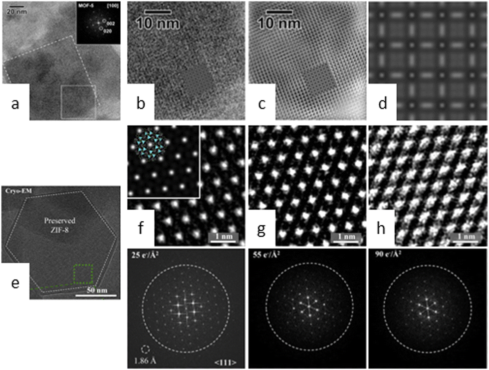 | ||
| Fig. 2 Cryo-EM images of MOFs. (a) HRTEM images of MOF-5. (b) Experimental image along the [100] direction. (c) Filtered image. (d) Simulated image. Reproduced with permission.35 Copyright 2012, Elsevier. (e) Cryo-EM image of ZIF-8 along the 〈111〉 direction. Electron doses of 25 e Å−2 (f), 50 e Å−2 (g), and 90 e Å−2 (h) with the corresponding FFT pattern. Reproduced with permission.38 Copyright 2019, Elsevier. | ||
Cryo-EM has recently emerged as a powerful technique for determining the nanostructure of proteins and energy materials, such as lithium batteries and perovskites.36,37 These examples suggest that a cryogenic environment may prevent structural devastation from beam damage. Li et al.38 developed a novel cryo-EM procedure for disclosing atomic host–guest structures within MOFs and demonstrated that these entities can be preserved at low temperatures for high-resolution imaging (Fig. 2e). The sample ZIF-8 underwent only partial amorphization when exposed to an accumulated electron dose of 90 e Å−2 at cryogenic temperature, whereas its crystallinity was completely destroyed when exposed to a dose of 50 e Å−2 at room temperature (Fig. 2f–h). Ogata et al.39 analysed the nucleation and growth of protein-MOFs using cryo-EM and disclosed the crucial stage of amorphous particle aggregation in triggering the dissolution–recrystallization process. Tong et al.40 attempted to ascertain the atomic-level structure of biomacromolecule-MOFs and the intrinsic relationship between their structure and activity. Notably, the cumulative dose of 30 e Å−2 for the optimal images is comparable to that used for MOFs and COFs at room temperature, indicating that although cryogenic temperatures can increase stability by several factors, it may not be a universal solution for extremely sensitive materials.
In this context, radiolysis has been identified as the primary mechanism responsible for the damage. Ghosh et al.26 used ZIF-8 to investigate the dominant damage mechanism by varying the incident electron dose rate from 2.91 to 0.34 e Å−2 s−1 (Fig. 3). Their findings indicated that, compared with inevitable knock-on damage, radiolysis is the leading cause of MOF destruction. Zhu et al.25 revealed that ZIF-8 crystals were obliterated by a cumulative dose of 25 e Å−2 and exhibited rapid crystallinity loss even at 1 e Å−2 s−1. They captured the motion-corrected images with a total dose of 4.1 e Å−2. Based on the strategy of combining multiple short-exposed images into one, they achieved an effective acquisition at a total dose of 10 e Å−2.41 This approach can distinguish certain metal atomic columns, distinct surface terminations, and benzene rings in organic linkers. It can be applied to a variety of other electron beam-sensitive materials, such as the organic–inorganic hybrid perovskite CH3NH3PbBr3. The study of ZIF-L revealed that at a dose of 25 e Å−2, the crystallinity suffered a noticeable loss, and completely collapsed at a dose of 100 e Å−2.42 At a cumulative dose of 50 e Å−2, the visible bend contours in individual ZIF-L particles diminish and eventually disappear. Peng and colleagues43 set the electron dose at 20 e Å−2, at which the honeycomb-like structure with individual construction blocks in the as-prepared ultrathin COF nanosheets can be plainly visualized. This is the first report on the atomic structure of COFs by high-resolution TEM (HRTEM) imaging.
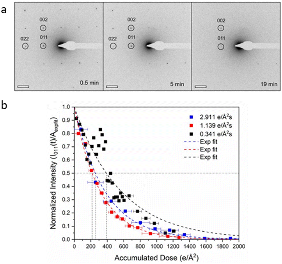 | ||
| Fig. 3 The effect of total dose on the crystallinity of MOFs. (a) Electron diffraction pattern of ZIF-8 at a dose rate of 0.34 e Å−2 s−1. (b) The intensities decrease at three different dose rates. Reproduced with permission.26 Copyright 2019, Oxford University Press. | ||
Besides the total dose, the dose rate also affects the damage and the corresponding deformation behavior. Zhou et al.27 used iDPC-STEM with a progressively increased beam current from 2 to 8 pA to ascertain the evolution process of MIL-101 crystals. The crystals exhibited bend behavior related to the specific facet and position to form distinct domains, as opposed to overall structure change with broken crystals. The d spacing shrank in all directions at almost the same rate as the accumulated dose increased from 28 to 46 e Å−2. When the beam current reached 8 pA, it was discovered that the (111) lattice plane contracted much more rapidly than the other directions. Similar electron irradiation was conducted on UiO-66 at a dose rate of 2.17 e Å−2 μs−1, and the acquired images demonstrated an increase in the contrast between the metal node and organic linkers with the increase in the total dose, corresponding to the release of organic linkers from the skeleton.44 In general, the rate of damage follows first-order decay kinetics stated as I/I0 = ê(−D/Dc), where Dc is the critical dose, which was determined as 256.41 e Å−2 in this case. Significantly, unlike uniform defects caused by ultra-low dose rate (4.38 e Å−2 μs−1), larger area nonuniform defects formed with the same accumulated dose but a high rate of 7.84 e Å−2 μs−1, indicating the influence of local charging and heating dominated by dose rate. Hence, minimizing the electron dose prior to their degradation is the most effective solution for precise atomic resolution images of beam-sensitive materials.
3. Technological innovations for low dose imaging
To prevent the collapse of multilevel ordered structures, low dose imaging has been identified as the primary solution. Nevertheless, ultralow doses can adversely affect image resolution, resulting in low SNR that can impede the atomic-level characterization. To achieve high-quality imaging under minimal doses, the first obstacle is the detector technology, which requires improving the detection efficiency of conventional CCD cameras. Innovative detectors, such as DEDs, have significantly increased detection efficiency, enabling the emergent application of low-dose imaging.28 The second factor that makes low-dose imaging more practical is the computer-assisted acquisition and interpretation of images under limited doses. Although zone-axis alignment and information rescanning can be time-consuming, recent advancements in computer technologies have significantly accelerated these processes. These advancements enable the analysis of complex information contained in images, including those that may be concealed behind a deceptive representation. In addition to image acquisition and analysis under low-dose conditions, sample processing to mitigate radiolysis damage is also a crucial factor.3.1 Innovations in detectors
CCD cameras have been a standard component in electron microscopes since the 1980s, providing real-time reading as an alternative to photographic films.29,45 These cameras typically consist of a scintillator that converts electrons to photons, which are then conveyed via fiber optics or lens coupling to generate electrical signals for readout (Fig. 4a). However, the SNR of CCD images is insufficient for the point-spread function, limiting their practicality. Moreover, the charges in CCD cameras must be read out pixel by pixel, after being transmitted row by row into a serial register (Fig. 4c). This readout process significantly limits their read rates and precludes their use for accurate specimen motion correction.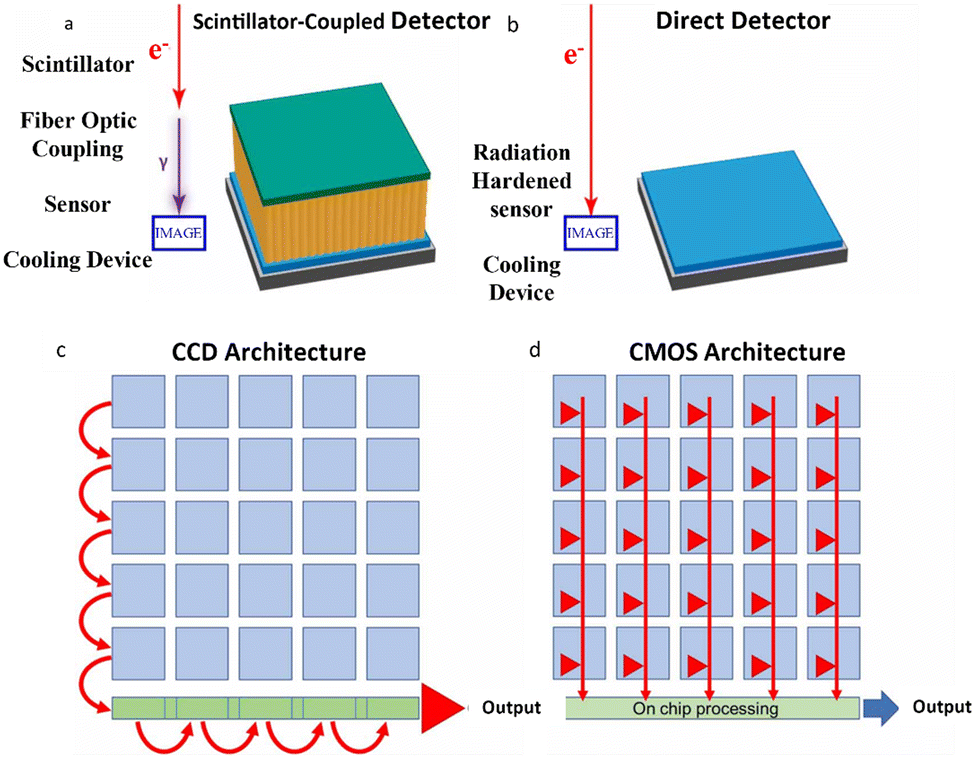 | ||
| Fig. 4 The difference between conventional CCDs and DEDs. (a) The electron–photon-sensor process in CCDs. (b) The electron-sensor process in DDEC. (c) The row-by-row readout architecture in CCDs. (d) The simultaneous readout architecture in every pixel in DEDs. Reproduced with permission.28 Copyright 2020, American Chemical Society. | ||
The direct conversion of electrons into an electronic signal can significantly increase the SNR and acquisition speed. The development of DEDs, such as the monolithic active pixel sensors (MAPs), has made this vision a reality that marked a turning point in TEM technology.28 By eliminating noise and signal distortions during electron–photon conversion and transfer (Fig. 4b), DEDs can provide a significantly higher quantum efficiency and SNR, resulting in the improvement of image qualities at a given dose. MAPs, with a narrow sensitive layer less than 30 μm, can receive a portion of the incident electron's energy and deposit it within a pixel, allowing for an enormous number of pixels more than 4000 × 4000 without back-scattering interference. Based on the high sensitivity of DEDs, which can convey signals even from a single electron, high spatial resolution imaging with rapid input and output speeds is achievable (Fig. 4d). Milazzo et al.46 reported that the enhanced capability of DEDs could be utilized in high quality 3D structure maps of biological samples under low dose with image drift correction, demonstrating the great potential of DEDs. Specifically, DEDs can increase the visibility of holographic fringes and decrease the statistical inaccuracy of the phase of the reconstructed electron wave function. They can also withstand higher dose rates, allowing dose rate optimization to achieve the highest phase resolution under a variety of experimental conditions. Therefore, the counting mode may be able to use a significantly lower dose while still achieving a phase resolution comparable to that of the linear method. During the detection of the oxygen K edge signal in a biological protein, the SNR in electron energy loss spectroscopy (EELS) is reported to be 10 times higher than that of traditional CCDs.47
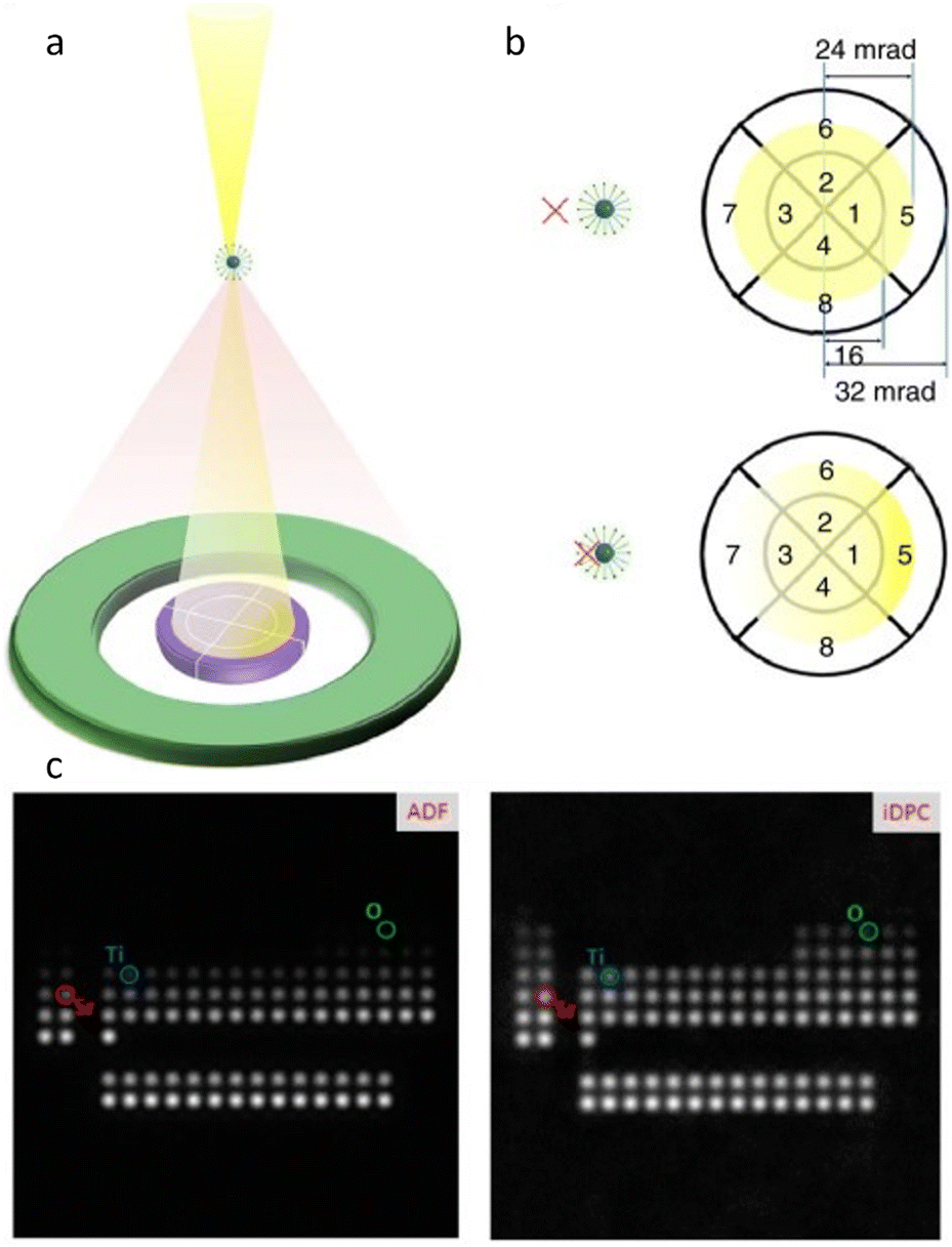
In contrast to the parallel beam used in TEM, STEM generates images by traversing a focused electron beam over the specimen, with signals including transmitted electrons and dispersed electrons detected by a bright field (BF) detector and annular detector, respectively. High angle annular dark field (HAADF) imaging is the most common modality for acquiring images with a high contrast proportional to Z1.5–2.0. However, it remains challenging to image heavy and light atoms simultaneously in HAADF-STEM. Furthermore, the limited utilization of incident electrons due to sparse scattering necessitates higher electron doses for acquiring high SNR images. Shibata et al.48 developed a new segment detector to thoroughly record the dispersed electrons and obtained 16 images simultaneously at the atomic level for post-processing. By calculating the difference between the signals taken by the opposing detector segments, the magnitude and direction of the electron beam's deflection can be measured quantitatively at each sample raster during beam scanning. The ability to record the localized and total electric and magnetic field of light and heavy element columns through the deflection is superior for constructing the exhaustive maps of the atoms' distribution, as opposed to the ambiguous “ghost” of the light atom in traditional methods.49,50 Lazić et al.30 proposed a continuously developed technology, iDPC-STEM, that demonstrates the approximately linear relationship between the diffraction disk's center of mass and its phase. iDPC-STEM can use almost all of the transmitted electrons to reduce the total electron dose for imaging (Fig. 5a and b).51 Their work on SrTiO3 demonstrated that even O atoms were clearly visible from iDPC-STEM images, while the corresponding information was absent in HADDF-STEM images (Fig. 5c).52 The integration procedure automatically applies physical regularization, suppressing the non-conservative portions of the noise field. iDPC-STEM has rapidly become one of the most prevalent low-dose imaging methods. Recent studies demonstrate the direct observation of molecules adsorbed in delicate porous zeolites at the atomic level, revealing different orientations caused by host–guest interaction in individual channels, elucidating atomic-level adsorption-catalysis processes.53,54
 | ||
| Fig. 5 The schematic illustration and imaging of the segment detector. (a) Segment detector inserted in the bright-field region and (b) intensity distribution for distinct probe position. Reproduced with permission.51 Copyright 2017, Springer Nature. (c) Simulated ADF-STEM and iDPC-STEM images of the periodic table of elements. Reproduced with permission.52 Copyright 2016, Oxford University Press. | ||
Besides the segment detector, hybrid pixel array detectors (HPADs), a subtype of DEDs, were developed to determine the phase of a specimen based on its atomic electrostatic potential.55 The thick sensor chips in HPADs, such as the electron microscope pixel array detector (EMPAD)56 in Fig. 6a and b, can capture all incident electrons to reconstruct the phase information, making them suitable for 4D-STEM acquisition. The detector records the 2D convergent beam electron diffraction (CBED) pattern for every dwell position in the 2D STEM raster over the specimen, enabling a 4D dataset to collect nearly all information about the specimen, including electric/magnetic field and strain. The synchronous readout of all pixels in HPADs can increase the recording speed with each pixel's real space and reciprocal space information to be read out.
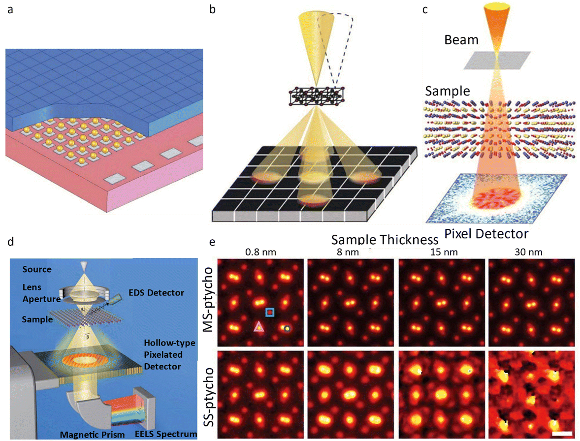 | ||
| Fig. 6 The pixel detector and schematic illustration for ptychography. (a) The illustration of the structure of the EMPAD. (b) The schematic illustration of 4D-STEM imaging by the EMPAD. Reproduced with permission.56 Copyright 2016, Oxford University Press. (c) Experimental setup for ptychography. Reproduced with permission.32 Copyright 2021, The American Association for the Advancement of Science. (d) Configuration for ptychography dataset acquisition. Reproduced with permission.62 Copyright 2018, American Physical Society. (e) The reconstructed images of PrScO3 with distinct thickness by multislice and single-slice ptychography. Reproduced with permission.32 Copyright 2021, The American Association for the Advancement of Science. | ||
Early 16 × 16 HPADs with a frame rate of 1.1 kHz had sufficient pixel density to distinguish distinct diffraction peaks, although slower than conventional STEM scan rates.55 The EMPAD significantly improved the SNR to 140 with a readout time of 0.86 milliseconds per frame and a high dynamic range of 106 for incident electrons.57,58 This remarkable dynamic range can help comprehensively map the specimen's physical information by describing features of interest with a wide variation in intensity. The second-generation EMPAD is capable of continuous imaging at a frame rate of 10 kHz, with a low-noise dynamic range extending from a single electron to 1.3 × 10⁷ electrons.59,60 The simultaneous high-precision measurements of all electrons suggest the possibility of extracting lattice information and strain maps from the complex datasets. Besides, a pixelated detector with 576 × 576 pixels was created with a frame rate up to 87 kHz, ensuring a data rate of 480 Gbit s−1 to record the data in minutes using fundamental edge computing algorithms.61
The information recorded in 4D-STEM can be used to construct virtual images like conventional STEM imaging such as HAADF and also can be applied to retrieve phase information by ptychography. Ptychography is based on the predictability of interference patterns during scanning and has been widely utilized in X-ray and optical microscopy. The technique is particularly attractive in electron microscopy due to the possibility of surpassing the information limit caused by the diffraction principle.
The challenges such as insufficient recording, inadequate dynamic range, and sluggish readout rates in ptychography can be resolved by utilizing HPADs, which offer a high dynamic range and synchronous readout of all pixels (Fig. 6d).62–64 Jiang et al.58 reported full-field ptychography using an EMPAD to decode phase information encoded in the diffraction pattern. The reconstructed image achieved a spatial diffraction-limited resolution of 0.39 Å, which is superior to the 0.98 Å resolution achieved by the conventional method under the same conditions. The atomic-resolution limits could be further improved to less than 20 pm by ptychography, corresponding to the thermal vibration of atoms (Fig. 6c and e).32 The future introduction of rapid hollow detectors, designed to work seamlessly with EELS spectrometers, facilitates concurrent correlative analysis incorporating Z-contrast, phase imaging (ptychography and DPC), and chemical mapping (EELS, EDS and secondary electrons) (Fig. 6d).62 Such multimodal STEM configuration offers multiple information channels about the specimen, ensuring efficient utilization of the electron dose.
3.2 Innovations in imaging procedures and acquisition
Modern detectors are indispensable for decoding the atomic structure of specimens. However, they alone are insufficient for implementing a practicable low dose strategy. The essential processes involve time-consuming image acquisition procedures, such as specimen searching, zone axis alignment, investigation of optimal imaging conditions, and image acquisition, resulting in excessive dosage waste.41 Even for seasoned researchers, evaluating the images and adjusting the corresponding parameters is a laborious process. Consequently, automated image acquisition and correction by computer technology can effectively reduce unnecessary time and minimize the overall accumulated dose. Unlike subsequent steps that require precise regulation, specimen searching does not rely on automatic operation and can be performed at extremely low dose rates of 10−3 e Å−2 s−1. While some automated systems have been developed to achieve effective detection without operator intervention, this is not a requirement for specimen searching.65Accurately aligning the zone axis is a primary challenge in controlling cumulative dose in TEM. Traditionally, the zone axis is progressively aligned by repeatedly toggling between imaging and diffraction patterns. This crucial stage enables the final visualization of the atomic distribution in the structure but comes at the expense of high dose consumption. Jansen et al.66 proposed an approach that combined the multislice method with a least-squares algorithm to rectify lattice misalignment with respect to the Laue circle, which performed well when the misorientation was small. Hayashida and collaborators67 presented a coarse-alignment based on a cross-correlation technique that presumes the tilt angle could range from α = −90° to 90°. This method worked well as an automatic pre-alignment prior to a precise zone axis alignment. Jansen et al.68 further improved the alignment procedure to achieve a high degree of precision up to 0.05–0.02° by recording a series of diffraction patterns. The dedicated open-source software ALPHABETA offers a simple user interface that allows users to calibrate the orientation of the specimen and then compute the tilt angles.69 This tool considerably reduces tilting work time by allowing for considerable tilts possible in image mode with approachable zones pre-indicated in the program. Zhang et al.41 designed a program to automatically calculate the deviated angle between the incident beam and the zone axis and conduct alignment accordingly. As shown in Fig. 7a–f, similar to the traditional method, the electron diffraction pattern is acquired to identify the orientation of the sample. The computer initially calculates the Laue circle by fitting the reflection positions to confirm the variation angle. The angle is then disassembled into α and β directions according to the TEM double tilt stage, and the following alignment based on the decomposed angle is implemented automatically. After the alignment, another diffraction pattern is collected to confirm the final orientation of the specimen. The same process is repeated until the alignment is nearly perfect. The number of measurements could be as low as two (several for perfect alignment), and the dose rate for diffraction can be decreased to 0.03 e Å−2 s−1. Then, the total dose for the whole zone axis alignment process can be far less than 1 e Å−2, significantly reducing the dose consumption before the final imaging. To realize a universal reorientation under a wide range of the misalignment angle, a program was developed to automatically index the diffraction patterns and tilt from a specific position (Fig. 7g).70 Under essentially the same procedure, an additional parameter about the crystal structure is necessary for a comprehensive evaluation about the orientation. As a result, the program can achieve a fast and precise alignment, and move the axis from one to another without manual operation under a deviation less than 0.6°.
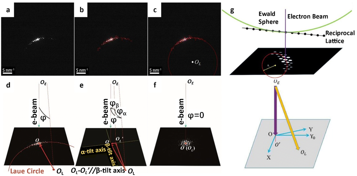 | ||
| Fig. 7 The automatic alignment of the zone axis. (a) The initial diffraction pattern acquisition. (b) Identification of reflection peaks. (c) Automatic fitting of the Laue circle and determination of the center OL. (d) Calculation of the angle between the zone axis and the incident direction. (e) The decomposition of the angle to α- and β-tilt axes. (f) The realization of the on-axis condition. Reproduced with permission.41 Copyright 2018, The American Association for the Advancement of Science. (g) The condition for a Laue ring and corresponding tilting to the Laue circle. Reproduced with permission.70 Copyright 2020, Elsevier. | ||
However, the optimal imaging conditions in HRTEM are typically judged by researchers instead of being tuned by computer. This is because the image contrast is affected by the defocus value, with the lowest contrast being observed when the specimen is in focus. The optimal defocus value, Scherzer defocus, is dependent on the spherical variance coefficient and electron wavelength of the objective. The phase contrast transfer function (CTF) obtains the defocus of the widest spatial frequency passband, enabling researchers to determine the in-focus position and thoroughly consider imaging under different defocus values. Koster et al.71 proposed an autofocus method by adjusting the beam's tilt and measuring the image displacement, followed by correction of the defocus based on the well-established association between the defocus and the displacement. While this method achieved a precision of 5 nm, it is not satisfactory for modern TEM imaging. To improve the accuracy and reliability of autofocus, further advancements have been made by operating under low-dose conditions and stretching the image before cross-correlation.72
Image acquisition is a critical process in low dose technology, but it remains challenging to achieve significant progress using conventional methods. To minimize the accrued electron dose in STEM, two conventional methods have been employed: decreasing the scanning dwell time on each pixel and reducing the number of incident electrons.73 However, these methods suffer from limitations such as the loss of stability of the scanning coil and potential misalignment due to the varied beam crossover. Recently, computer technology has provided an alternative method for low dose image acquisition using compressed sensing (CS).74 In conventional sampling methods, the signal taken from the full sampling model can be used to reconstruct the image perfectly. However, under-sampled measurements, which compress the signal, can be reconstructed using a mathematical algorithm that considers a priori knowledge of the signals. Thus, perfect reconstruction from under-sampling can replace the fully sampled method, thus reducing the sampling rate and exposure time for low dose imaging. CS was first applied in electron tomography, a technology used to reconstruct the 3D morphology of specimens, to recover images from incomplete signals.75 Saghi et al.76 analysed the 3D structure of iron oxide nanoparticles with improved reconstruction quality including fewer missing wedges, providing reliable quantitative analysis without tedious projections. To achieve dynamic and real-time imaging, a dynamic CS framework was developed.77 After the initial projection is acquired, the reconstruction process begins instantly and dynamically modifies the 3D structure as subsequent projections come. Dynamic CS is a continuous optimization that accommodates extra restrictions introduced by fresh projections.
CS has the potential to revolutionize low dose imaging, and its application in STEM has been explored using Bayesian dictionary algorithms. The algorithms were applied to a set of under-sampled images, where the number of pixels was reduced to 5% of the original. Despite this substantial reduction, the algorithms successfully reconstructed the original picture, showcasing their effectiveness in dealing with under-sampled pixel data. The post-acquisition image alterations could be immediately applied as a low-dose acquisition approach without changes to the electron optics or the microscope's alignment.80 It is proposed that a coded aperture CS can integrate a series of images into a frame after decompression according to the extent of damage, rather than recording both damaged and undamaged part in the same image (Fig. 8a–c).78 This method can help rebuild the precise commencement of radiolysis, and allow for a speedup of more than an order of magnitude.81 The corresponding methodologies to realize the CS in this manner include blanking the incident electrons between two lighted pixels or guiding the scanning coils in a certain way to leap from one illuminated pixel to a nonadjacent subsequent pixel.79 Efficient random sampling can reduce the dose for atomic-resolution images by at least 5 times (Fig. 8d–f). In addition to the slump in accumulated dose (even lower than 1 e Å−2) for atomic resolution, the sub-sampling method exhibited a faster acquisition rate, exceeding 10 times, as well as enhanced resolution.73 These advantages ensure a more realistic determination, especially for the in situ observation which can last quite a long time.82 The subsampled method minimizes the interference of the external incident beam in in situ observation, and can illustrate the most actual reaction process at spatial/temporal resolution.
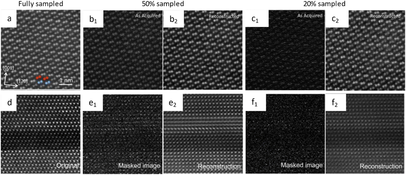 | ||
| Fig. 8 The schematic illustration of CS and the reconstructed images. Images of NiTiO3 acquired under (a) fully, (b) 50%, and (c) 20% sampled conditions. Reproduced with permission.78 Copyright 2016, AIP Publishing. Images of the complex perovskite sample acquired under (d) fully, (e) 50%, and (f) 20% sampled conditions. Reproduced with permission.79 Copyright 2016, AIP Publishing. | ||
3.3 Innovations in computational processing and analysis
The low dose technique has flourished with the constant development of detectors and imaging technologies, enabling reliable acquisition of images at atomic resolution. However, partial images are still affected by a trade-off in decreased SNR. Therefore, post-processing techniques such as denoising have become crucial for rigorous and compressive measurements to extract the information from unimpressive and low contrast regions. In the conventional approach, adaptive nonlinear filters utilize local SNR to calculate a suitable factor ratio for eliminating noise from an image contaminated by a mixture of indistinct additive random noise. This methodology guarantees the preservation of edge details while mitigating noise interference. Furthermore, the phase retrieval, which can reconstruct the fully structured images with phase information, has also seized the opportunity to apply the computer technique in the complicated mathematical reconstruction. The resulting images through post-processing techniques match well with the realistic structure at the atomic level.32 Finally, to decipher these images, deliberate simulations taking into consideration the interaction between incident electrons and atoms are required to interpret the experimental measurements. The combination of low dose techniques, advanced post-processing, and sophisticated simulation has facilitated the acquisition of atomic-resolution images with exceptional detail and precision.Additionally, this approach offers more flexibility in adjusting illumination according to practical conditions. Broek et al.92,93 successfully retrieved the 3D potential of a specimen using a neural network based on the multislice strategy for a non-heuristic treatment of the modulation transfer function. In their further investigation, a similar treatment involving the combination of forward-simulation algorithms was conducted to recover the 3D structure from CBED patterns.94 The versatile algorithm is theoretically suitable for other parameters associated with the interaction between the electron beam and the specimen, especially for limited measured disks with realistic noise even in the cases where there is a mismatched mean intensity.
Simulation is a time-consuming process with multiple central processing unit cores, especially for models with thousands of atoms. The combination with intuitive GPU can significantly decrease the calculation time, even on a desktop computer.105–108 Several open source codes or software, such as QSTEM,109 STEM_CELL,110 MULTEM,106 FDES,107 EMsoft,111 Prismatic,112 Dr. Probe,113 and ToTEM,114 have been developed for practical simulation.
Additionally, the introduction of CS technologies, which are successfully applied in TEM imaging, has also promoted the development of simulation. The sub-sampling method for signal acquisition and subsequent recovery of missing information using inpainting algorithms show great potential to combine with STEM simulation for an agreement with the simulated images from the fully sampled mode.115,116 This advanced method can significantly reduce the simulation time, as well as the electron dose for sensitive materials. Further CS methods have been proposed to sample each layer in the frozen phonon model at a much lower ratio, which may allow for real-time STEM simulation.117
3.4 Innovations in specimen protection
Innovations in (S)TEM instrumentation and computational techniques have focused on image acquisition and processing to address fundamental factors. The successful application of these techniques has ensured comparable imaging quality at a lower dose of several orders of magnitude, ranging from 1010 to even below 10 e Å−2. As a vital method for preparing specimens with suitable thickness, the focused ion beam (FIB) method may introduce ion beam damage into materials. Therefore, a cryogenic system has been introduced to the conventional FIB to minimize the damage. Additionally, at ultra-low electron dose, any measures to prolong the dwell time will enhance the imaging quality. Hence, coating of the specimen with a protective layer can remarkably reduce the amount of surface sputtering, and effectively delay the beam damage.The cryogenic system, a routine method used in TEM for characterization of biological specimens, has been integrated into FIB to process the beam-sensitive samples.130–132 It has been shown that the samples fabricated by cryo-focused ion beam (cryo-FIB) milling have negligible devitrification and artifacts compared to those obtained by conventional cryo-ultramicrotomy. Cryo-FIB milling is simpler and requires less specialized personnel than cryo-sectioning, making it widely applied in cryo-TEM.133–135 Similar protection from ion beam damage has also been explored in polymer films that suffer from beam heating due to low conductivity. The results showed enhanced tolerance to beam current by nearly 10 times.136
The successful use of cryo-FIB in battery materials inspired the investigation of its applications in beam-sensitive materials.137 Cryo-FIB minimizes surface damage and re-deposits of Li-metal materials by freezing samples at −170 °C throughout processing, which solves the sensitivity, artifact difficulties, and mechanical deformation of conventional sample cross-sectioning, as well as allowing for a quantitative evaluation of deposited Li (Fig. 9c and d).138,139 Cryo-FIB has also been applied to the processing of metals and their alloys,140 solid–liquid interfaces and reactive materials,141 solar cells,142 and more.143,144 Recently, pioneering work on the application of cryo-FIB in ultra-sensitive materials, MOFs and hybrid halide perovskites was reported (Fig. 9a and b).145 It maintained perfect crystallinity at 16 kV compared to total crystallinity loss at room temperature (Fig. 9e and f). Furthermore, the universality of cryo-FIB was investigated in the determination of MOF–COF core–shell structures.146 This approach effectively preserves the crystallinity of the materials throughout the process. Cryo-FIB also enabled orientation predetermination, which is particularly relevant for materials with various constituents or preferred orientations.
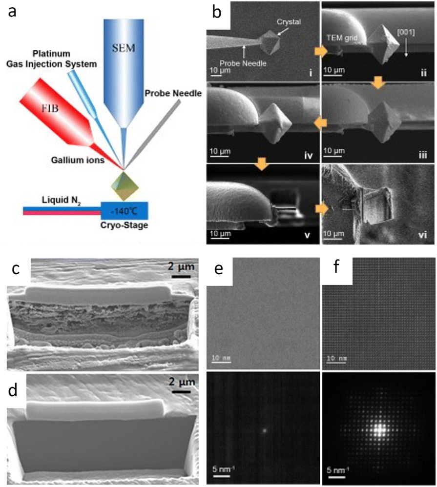 | ||
| Fig. 9 Cryo-FIB for sample preparation. (a) Scheme of a cryo-FIB dual-beam system. (b) Workflow of cryo-FIB. Reproduced with permission.145 Copyright 2013, AIP Publishing. (c, d) The SEM image of cross-sectioned Li foil at (c) room temperature and (d) cryogenic temperature. Reproduced with permission.139 Copyright 2019, American Chemical Society. (e, f) HRTEM image and the corresponding electron diffraction pattern of HKUST-I prepared at (e) room temperature and (f) cryogenic temperature with 16 kV ion beam for milling. Reproduced with permission.145 Copyright 2013, AIP Publishing. | ||
Graphene, which exhibits significant protective capability as a chamber for bacterial cell observation148 and in ion irradiation,149 may enhance the resistance of materials to electron damage. It has been reported that the radiation resistance of the initial single layer of MoS2 was improved by three orders of magnitude through coating two graphene layers to form a sandwich layered structure, which allows for pristine atomic inspection of MoS2.150,151 The subsequent successful application of this strategy in the atomic characterization of MoTe2,152 phosphorene,153 and perovskites154 demonstrates that coating can remarkably enhance stability. It has been mentioned that the edge of the sandwich sample is less stable than the interior area, and may transform into an amorphous structure first.152 Molecular dynamics simulations based on separation of the dimension and encapsulation have revealed substantial cooperation in toleration to radiolysis. The simulation results showed a hundred-fold increase in resistance from 3D to 1D.155 Therefore, the combination of sample functionalization, encapsulation, and advanced low dose imaging technologies may provide a viable approach to investigate the structure and dynamic behavior of materials at atomic resolution over long time periods.
4. Current implementations in COMs
The utilization of a diverse range of organic groups has significantly broadened the spectrum of MOFs and COFs. Various chemical reactions are employed for linkage formation, leading to morphologies ranging from 0D to 3D. The frameworks demonstrate diverse applications, including gas capture and separation, photocatalysis, electrocatalysis, and device fabrication. Accurately determining the atomic-scale skeleton of these frameworks is crucial to establish the relationship between structure and performance, which can enhance understanding of the fundamental principles of physics and chemistry and facilitate the design of functionalized materials with specific properties. The recent rapid development of low dose (S)TEM imaging techniques has demonstrated an unprecedented opportunity for the determination of the atomic-scale structure of MOFs and COFs in multiscales and multidimensions. These techniques have enabled the observation of details such as atomic defects, host–guest interaction, and surface structures, with a resolution previously unattainable.4.1 HRTEM
![[3 with combining macron]](https://www.rsc.org/images/entities/char_0033_0304.gif) m space group were presented. Since then, HRTEM has gradually become a routine characteristic method to verify the crystal structure of MOFs and for further elucidating the local structure.34,157,158 For example, a pyridine-stabilized MOF exhibited improved resistance to electron irradiation due to the introduced pyridine units.157 In Fig. 11a, HRTEM images of 2D hexaaminobenzene-derived MOFs were taken with a low dose rate of 1 e Å−2 s−1.159 The honeycomb array with holes smaller than 1 nm, as predicted by the 2D eclipsed packing model from PXRD, was validated by HRTEM images. Complementary strategies, including DEDs, automated zone axis search, image alignment, and calculation of the defocus value, were used to decrease the cumulative dosage for time-consuming modification required under ideal imaging conditions.41 The use of an ultra-low dose of 0.033 e−1 per pixel in each frame ensured that the acquisition was completed before damage occurred. As shown in Fig. 10, HRTEM images with high SNR were in excellent agreement with the crystal structure of UiO-66, which consisted of triangular channels encircling metal clusters and 1,4-benzenedicarboxylic acid (BDC) linkers, as well as Zr atomic columns inside the Zr6O8 clusters.
m space group were presented. Since then, HRTEM has gradually become a routine characteristic method to verify the crystal structure of MOFs and for further elucidating the local structure.34,157,158 For example, a pyridine-stabilized MOF exhibited improved resistance to electron irradiation due to the introduced pyridine units.157 In Fig. 11a, HRTEM images of 2D hexaaminobenzene-derived MOFs were taken with a low dose rate of 1 e Å−2 s−1.159 The honeycomb array with holes smaller than 1 nm, as predicted by the 2D eclipsed packing model from PXRD, was validated by HRTEM images. Complementary strategies, including DEDs, automated zone axis search, image alignment, and calculation of the defocus value, were used to decrease the cumulative dosage for time-consuming modification required under ideal imaging conditions.41 The use of an ultra-low dose of 0.033 e−1 per pixel in each frame ensured that the acquisition was completed before damage occurred. As shown in Fig. 10, HRTEM images with high SNR were in excellent agreement with the crystal structure of UiO-66, which consisted of triangular channels encircling metal clusters and 1,4-benzenedicarboxylic acid (BDC) linkers, as well as Zr atomic columns inside the Zr6O8 clusters.
 | ||
| Fig. 10 The low-dose HRTEM images of MOFs. (a)–(d) The raw (top) and denoised (bottom) images of UiO-66 from different zone axes. (e) Drift-corrected, and (f) CTF-corrected and Wiener-filtered images of ZIF-8. (g) Drift-corrected, and (h) CTF-corrected and Wiener-filtered images of HKUST-1. Reproduced with permission.41 Copyright 2018, The American Association for the Advancement of Science. | ||
Low-dose HRTEM enables the determination of the exact atomic structure of MOFs with discernible defects for specific functions related to defect engineering.160 Low-dose HRTEM images in Fig. 11e–g revealed the coexistence of “missing linker” and “missing cluster” structural defects from distinct projections and electron crystallography. In the presence of the prevailing missing-linker defect, UiO-66 experienced a topological transformation from a face-centered cubic to a body-centered tetragonal structure. In contrast, missing cluster defects only manifest themselves in a constrained space and result in two different underlying topologies of reo and scu net. The defect tuning technique enables an intuitive investigation of the relationship between defects and catalytic performance. As an example, Chen et al.161 doped Ni into Zn-MOFs based on the assumption that the square-planar coordinated Ni2+ could only replace the Zn on the crystal surface. A crisp image of (110) facets in rhombohedral dodecahedron crystals, together with energy-dispersive X-ray spectroscopy (EDS), was used to calculate the number density of metal atoms, indicating a density of 0.5Ni atoms per square nanometer.
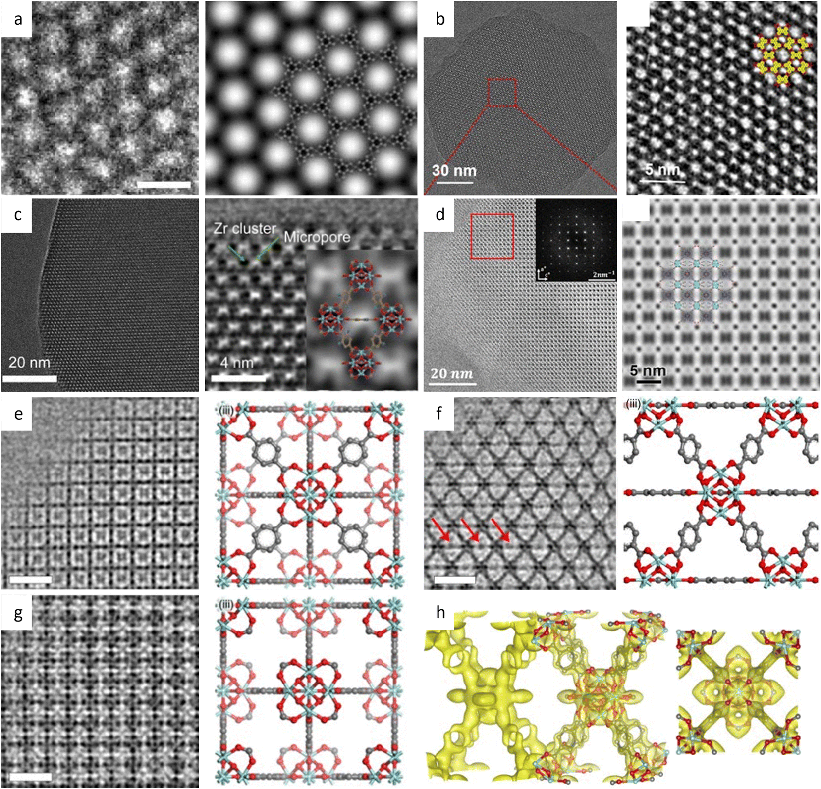 | ||
| Fig. 11 The low-dose HRTEM images of MOFs. (a) The raw image, and symmetry-imposed and lattice-averaged image of Cu-/Ni-HAB MOFs. Reproduced with permission.159 Copyright 2018, Springer Nature. (b) Images of kgm-TBA-MOF. Reproduced with permission.165 Copyright 2023, American Chemical Society. (c) The raw image and CTF-corrected image of UiO-66-NH2, inset: model of UiO-66-NH2. Reproduced with permission.164 Copyright 2023, Elsevier Inc. (d) Image of PCN-226(Cu) along the [010] direction with the corresponding Fourier transform, and symmetry-imposed image. Inset: Model of PCN-226(Cu). Reproduced with permission.170 Copyright 2020, American Chemical Society. CTF-corrected images of UiO-66 along the (e) [001], (f) [110], and (g) [001] zone axes. (h) Reconstructed 3D electrostatic potential map from different directions. Reproduced with permission.160 Copyright 2019, Springer Nature. | ||
Low dose HRTEM, in conjunction with advanced cryo-FIB techniques, provides more details about the intrinsic structure of MOFs, and allows for comprehensive reconstruction of their 3D structure.145 In the determination of defects in MOF HKUST-1, ultralow-dose HRTEM images showed that an interpenetrating structure would form due to the overlap of two sets of lattices after the split and shift of a single crystal, resulting in a locked boundary with a distance of 3.2 Å. Robison et al.162 designed a non-interpenetrated Zr cluster-based MOF, and determined the structure of original NU-1200 and its evolutive interpenetrated STA-26. They created a script to extract the Fourier transform of the area of interest and employed statistical methods to determine the predominant form based on the relative intensity ratios. The results indicated that once an interpenetration transition is initiated, it happens swiftly and thoroughly. A novel Fe-MOF, DNF-9, showed fluorinated metal nodes packed in an alternating helical pattern based on HRTEM images.163 At an ultra-low dose rate of 0.03 e Å−2 s−1, the structure of the UiO-66-NH2 derivative was determined.164 The resulting highly crystalline structure with octahedral morphology clearly showed Zr6O8 clusters with abundant defects caused by missing linkers as shown in Fig. 11c.
To increase the interlayer π–π contacts, a flexible non-planar molecule with a large molecular size core was utilized to synthesize the 2D conductive MOFs.165 For instance, the sql-TBA-MOF with a single pore showed a nanorod morphology with a lattice fringe distance of 1.52 nm for the (110) plane, while the kgm-TBA-MOF with a kagome topology with hexagonal and triangular dual pores featured a hexagonal nanoflake morphology with a lattice fringe distance of 2.6 nm for the (100) plane (Fig. 11b), demonstrating the viability of the topological control method. Sun et al.166 reported a kind of nanowire-liked MOF with a pore size of 1.4 nm at a dose of 1.5–5.6 e Å2. Another type of nanowire-like MOF, Zn-HHTP-H2O, synthesized from octahedral Zn(II), exhibited an AB stacking model and a honeycomb structure with a width of 12 Å in the [001] direction.167 Taking a novel approach to integrate Ni–S into the coordination links, a bamboo-leaf-like Ni(DMBD)-MOF was synthesized, and the lattice fringe distance of the contained crystal nanosheets could be recognized as 9.5 Å from a side view.168 Furthermore, the HRTEM images displayed a distinct (010) twin border along the [101] and [101] zone axes. Gong et al.169 combined TEM imaging (dose around 10 e Å−2) with metalation of linkers to differentiate between porphyrinic MOFs that would be indistinguishable by other methods.
A technique based on the use of Zr-chains was developed for high chemical and redox stability, and to tune the separation of redox active sites at an optimal density.170 The HRTEM images in Fig. 11d revealed rectangular packing along [010] with an interplanar spacing d200 of 18.32 Å, which matched well with the simulation model. To solve the limited processability of MOF powders, a new approach was developed that involved the hybridization of block copolymers with active sites for metalation with MOFs through self-assembly.171 The alternate layered structure corresponding to the Zr-rich or Zr-deficient regions could be identified, and the building unit results in a lamellar structure with a width of about 4.2 nm.
Identifying the structure of COFs encounters more challenges due to their poor crystallization and substantial overlap. A two-step seeded approach was proposed to fundamentally resolve the inadequate controllability of nucleation and growth processes.172 This approach polymerizes monomers to create crystalline COF nanoparticles as seeds. The gradual addition of more monomers controls the second polymerization, resulting in single crystalline COFs with large domains. By separating the processes, growth occurs on the surface of existing nanocrystals instead of new particles. As a result, the targeted COFs presented single crystal domains with size up to 1.5 μm. At a total dose of 26.5 e Å−2, COF-5 showed lattice fringes consistently and continuously extending from edge to edge. Intriguingly, despite possessing a comparable hexagonal structure and continuous crystalline domains, COF-10 exhibited a preference for orientation stacking perpendicular to the substrate. This method was subsequently extended to synthesize the single-crystalline boroxine-linked 2D and 3D COFs through the dehydrative trimerization of polyboronic acids.173 The single-crystalline nature of the 2D and 3D samples was clearly identified while a variation existed in the interlayer distance for stacking offset in the 2D crystals.
Due to the poor conjugation of boroxine COFs, colloidal COF nanoparticles connected by imine were synthesized for photoelectronic applications.174 HRTEM imaging revealed that TPB-MeOTP-NP and TPBMeOTP-NS had identical honeycomb networks but with a plate-like and spherical morphology, respectively. The centimeter-scale homogeneous films fabricated using the COF nanoparticles were incorporated in photoelectrodes for photoelectrochemical solar-to-hydrogen conversion, and their performance was comparable to the best performance of conventional semiconductor-based photocathodes.
Imines are the most prevalent and adaptable class of COFs, and they are intensively researched to determine an effective strategy to produce high-quality COF single crystals under moderate conditions. Single crystals of 2D COFs with a size range of 4–20 μm were produced by the solvothermal method in only 5 minutes.175 Constant lattice fringes extending from edge to edge of the platelets indicate the integrity of the single crystal. The inter-lattice fringe distances were measured to be 24.0 Å and 31.5 Å for TAPPy-PDA and TAPB-DMPDA, respectively. After inserted into gas chromatography separation columns, single-crystalline COFs showed a considerable increase in efficiency and selectivity compared to polycrystalline COFs, indicating the importance of the highly ordered structure. In a recent study, inverse pulse gas chromatography was used to quantitatively characterize the physiochemical adsorption properties of these 2D COFs.176 The results demonstrated that the single-crystalline TAPPy-PDA COF exhibited a nonpolar and electron donor character, whereas the reference polycrystalline sample exhibited a mild polar and electron acceptor character.
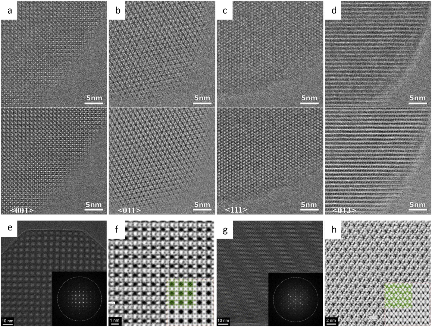
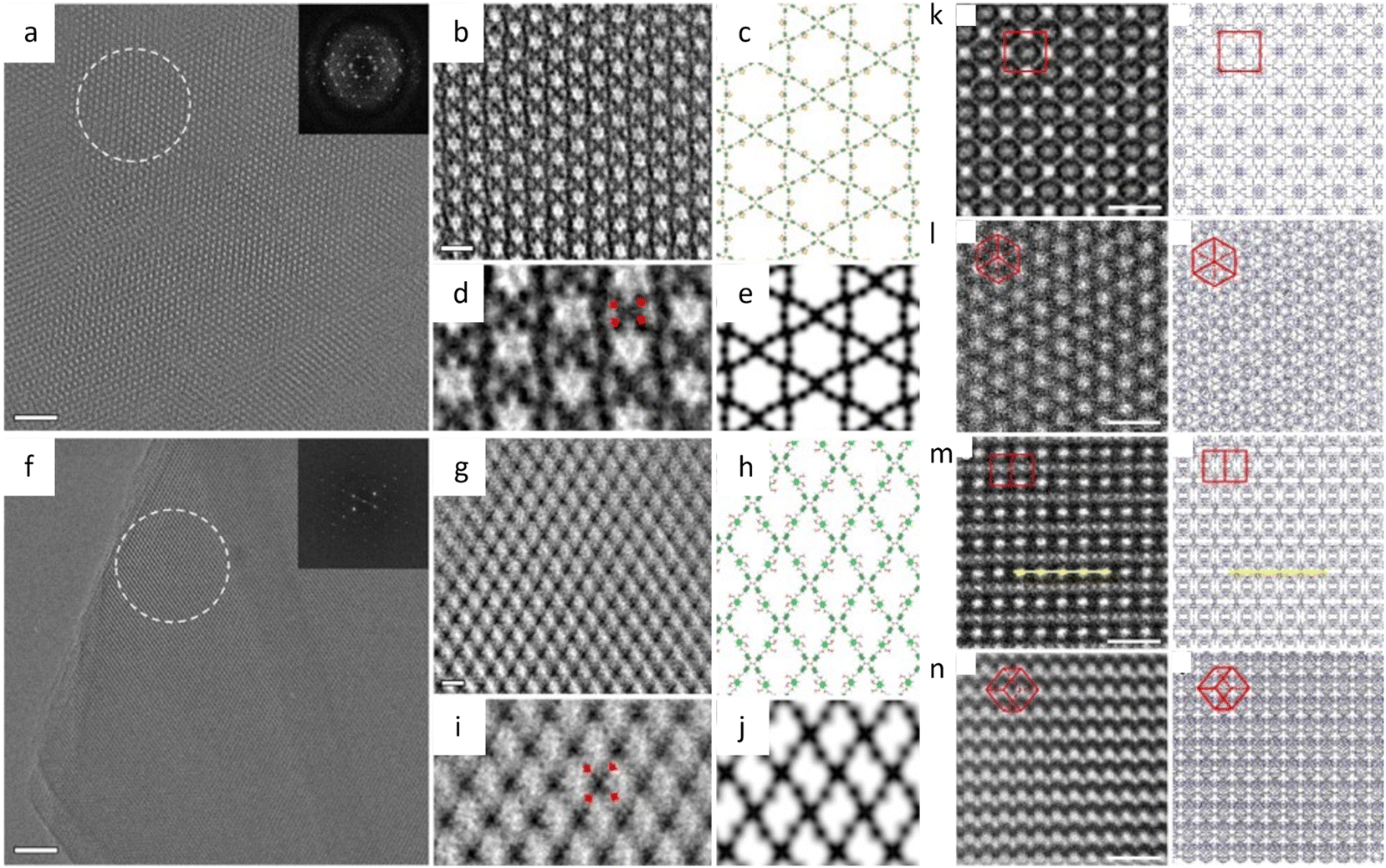
The facile synthesis of imine-based COFs permits a direct comparison of the alterations in properties resulting from structural isomers, such as the orientation of the C![[double bond, length as m-dash]](https://www.rsc.org/images/entities/char_e001.gif) N bonds.177 In contrast to its isomer, the TAPAPDA COF exhibited perfect reversibility in phase transition involving the slip-stacking model of the β phase, coupled with a high solvatochromic feature. The imine linkages also permit the introduction of antiaromatic compounds for intriguing attributes, such as a low HOMO–LUMO energy gap.178 Dibenzopentalene-based building blocks with an antiaromatic 4n π-conjugated structure are stable in both oxidized and reduced states, making them suitable as electrode materials. The crystalline nature of the COFs is demonstrated by rod-shaped crystals with constant (200) lattice fringes of 1.24 nm, enabling a higher capacity as a positive electrode material in Li-organic batteries (26 mA h g−1) compared to amorphous DBP-Ph-TFP POP (14 mA h g−1). The imine linkages could also be transformed to more resistant quinoline linkages while preserving the original topology and porosity.179 HRTEM images (Fig. 12a–d) at a cumulative dose of 2.1 e Å−2 revealed an ordered hexagonal projected symmetry with a pore size of approximately 3.0 nm. After the transformation through cycloaddition, the pore size suffered a modest drop to around 2.3 nm while maintaining its original structure. The quinoline aromatic ring-linked COFs displayed significantly increased stability against strong acids and bases. The intramolecular Povarov reaction that can transform imine linkages to more stable chromenoquinoline moieties was also applied in the formation of crystalline COFs with ladder-type linkages from single-strand-type linkages (Fig. 12e–h).180 In addition, transformation via the three-component Doebner reaction has been applied to synthesize stable crystalline COFs.181 The resulting COFs with an interplanar d-spacing of 0.34 nm in HRTEM images exhibited superior crystallinity and stability compared to imine COFs. To construct COFs with pre-designed topology, introducing molecular linkers with variable conformation has been developed to provide an extra degree of freedom for the topologies.182 As shown in Fig. 13a–i, two distinct COFs were synthesized using TPE links: one with a dual-pore kagome topology (TPE-COF-OH) and the other with a single-pore rhombic topology (TPE-COF-OMe). HRTEM images revealed a star-shaped hexagonal project structure in TPE-COF-OH, featuring a triangular channel with a pore size of 7 Å and a hexagonal channel with a pore size of 27 Å. In comparison, a rhombic-shaped projected structure was observed in TPE-COF-OMe, with a pore size of 12 Å.
N bonds.177 In contrast to its isomer, the TAPAPDA COF exhibited perfect reversibility in phase transition involving the slip-stacking model of the β phase, coupled with a high solvatochromic feature. The imine linkages also permit the introduction of antiaromatic compounds for intriguing attributes, such as a low HOMO–LUMO energy gap.178 Dibenzopentalene-based building blocks with an antiaromatic 4n π-conjugated structure are stable in both oxidized and reduced states, making them suitable as electrode materials. The crystalline nature of the COFs is demonstrated by rod-shaped crystals with constant (200) lattice fringes of 1.24 nm, enabling a higher capacity as a positive electrode material in Li-organic batteries (26 mA h g−1) compared to amorphous DBP-Ph-TFP POP (14 mA h g−1). The imine linkages could also be transformed to more resistant quinoline linkages while preserving the original topology and porosity.179 HRTEM images (Fig. 12a–d) at a cumulative dose of 2.1 e Å−2 revealed an ordered hexagonal projected symmetry with a pore size of approximately 3.0 nm. After the transformation through cycloaddition, the pore size suffered a modest drop to around 2.3 nm while maintaining its original structure. The quinoline aromatic ring-linked COFs displayed significantly increased stability against strong acids and bases. The intramolecular Povarov reaction that can transform imine linkages to more stable chromenoquinoline moieties was also applied in the formation of crystalline COFs with ladder-type linkages from single-strand-type linkages (Fig. 12e–h).180 In addition, transformation via the three-component Doebner reaction has been applied to synthesize stable crystalline COFs.181 The resulting COFs with an interplanar d-spacing of 0.34 nm in HRTEM images exhibited superior crystallinity and stability compared to imine COFs. To construct COFs with pre-designed topology, introducing molecular linkers with variable conformation has been developed to provide an extra degree of freedom for the topologies.182 As shown in Fig. 13a–i, two distinct COFs were synthesized using TPE links: one with a dual-pore kagome topology (TPE-COF-OH) and the other with a single-pore rhombic topology (TPE-COF-OMe). HRTEM images revealed a star-shaped hexagonal project structure in TPE-COF-OH, featuring a triangular channel with a pore size of 7 Å and a hexagonal channel with a pore size of 27 Å. In comparison, a rhombic-shaped projected structure was observed in TPE-COF-OMe, with a pore size of 12 Å.
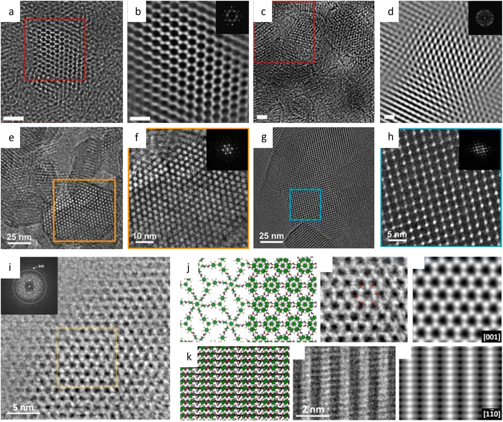 | ||
Fig. 12 Low-dose HRTEM images of COFs. (a) High-resolution image and (b) Fourier-filtered image of COF-1. (c) High-resolution image and (d) Fourier-filtered image of MF-1a. Reproduced with permission.179 Copyright 2018, Springer Nature. (e) and (f) Images of CQ-COFTAPB-BPTA. (g) and (h) Images of CQ-COFPy-BPTA. Reproduced with permission.180 Copyright 2022, American Chemical Society. (i) CTF-corrected image of HFPB-TAPT. (j) Single-layer and ABC stacked model along the [100] direction, enlarged image from (i), and simulated image (from left to right). (k) Structural projection along the [1![[1 with combining macron]](https://www.rsc.org/images/entities/char_0031_0304.gif) 0] direction, raw image, and simulated image (from left to right). Reproduced with permission.183 Copyright 2022, American Chemical Society. 0] direction, raw image, and simulated image (from left to right). Reproduced with permission.183 Copyright 2022, American Chemical Society. | ||
 | ||
| Fig. 13 Low-dose HRTEM images of COFs. (a) Raw image, (b) CTF-corrected image, (c) structural model, (d) motif-averaged image and (e) simulated image of TPE-COF-OH. (f) Raw image, (g) CTF-corrected image, (h) structural model, (i) motif-averaged image and (j) simulated image of TPE-COF-OMe. Reproduced with permission.182 Copyright 2020, American Chemical Society. Images and projections of catena-COF-806 along the (k) [001], (l) [111], (m) [10], and (n) [12] direction. Reproduced with permission.184 Copyright 2023, Springer Nature. | ||
By selecting monomers with the highest C6-symmetry, researchers designed COFs with kgd topology that could lead to the smallest pore size.183 HRTEM images in Fig. 12i–k revealed a honeycomb pattern with a decreased p3 symmetry in the [001] direction, indicating a more stable configuration, as well as a distinguishable ABC stacked structural projection in the [110] direction. HFPB-TAPT, with the smallest pore size of 6.5 Å, exhibited the maximum loading quantity and excellent release characteristics in drug delivery. Recently, a set of distinctive COFs comprised of mechanically interlocked catenanes have been constructed to investigate the facilitating dynamics of such an interlocked structure (Fig. 13k–n).184 An unprecedented [∞] mechanically linked framework in COFs is realized by an infinite 3D arrangement of the alternately linked tritopic linker and tetrahedral Cu(PDB)2BF4. The spots in catena-COF-805 are aligned in a zigzag pattern along the 〈10〉 direction, but they are aligned in a straight line in the other two samples, which may be due to the unit-cell doubling in catena-COF-805. All three COFs display a doubly interpenetrated bor-y topology, while the space group of catena-COF-805 is identified as F4132, whereas catena-COF-806 and 807 are P4232. To prevent the reduction of surface area due to interpenetration in topologies like pts, innovative 3D COFs based on the stp topology with non-interpenetration have been developed.185 These COFs exhibited both high surface area and exceptionally low crystal density. The HRTEM images clearly showed channels with a hexagonal structure, and the (100) and (010) reflections had a d-spacing of 4.65 nm, which is in good agreement with the proposed structural model.
 | ||
| Fig. 14 Synthesis and low-dose HRTEM characterization of 2D nanosheets. (a) Schematic illustration of the 2D nanosheet synthesis by the exfoliation method. (b) Motion-corrected image, (c) CTF-corrected and denoised image, and (d) simulated potential map of 1-MONs. Reproduced with permission.186 Copyright 2021, American Chemical Society. (e) Cryo-EM image, (f) enlarged image, and (g) averaged image of the Cu3HHTT2 MOF. Reproduced with permission.189 Copyright 2020, Springer Nature. | ||
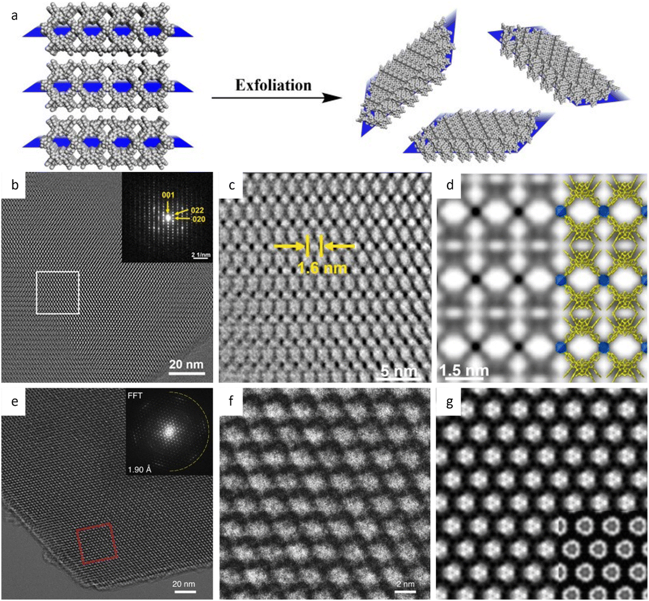
Additionally, a bottom-up strategy based on building block design has been proposed to synthesize 2D MOFs, taking cues from the finding that incorporating a larger proportion of the π-conjugated structure into the skeleton will enhance non-covalent interactions.189 By choosing a large, electron-deficient ligand core with lower electron density, direct synthesis of 2D MOFs with improved in-plane crystallinity has been achieved. The HRTEM images in Fig. 14e–g exhibited a long-range ordered array with a pore size of 2.1 nm, which agrees with the result of N2 adsorption isotherm and simulations. As anticipated, the 2D MOFs exhibited anisotropic electrical transport capability, with the in-plane conductivity of the whole crystallite significantly greater than that of the out-of-plane conductivity. An alternative bottom-up technique, based on anisotropic nature of horizontal and vertical directions, has been developed to promote a preorientation of the ligand on the surface.190 HRTEM observations clearly demonstrated a large crystalline domain of 600 nm with a distinct lattice distance of 1.75 nm and a π–π stacking distance of 0.33 nm. The 2D film exhibited three orders of magnitude greater conductivity horizontally than vertically. More recently, unit-cell-thick MOF films, ranging from sub-monolayers of 2 nm to several layers, were synthesized on substrates by controlling growth time and precursor concentration.191 HRTEM images revealed alternating chains of 4-membered and 6-membered rings along the [001] direction, which features the films with an outstanding gas sieve performance, with a separation factor of 115 in H2/N2 separation. The same approach can also be applied to fabricate 2D COF nanosheets. Peng et al.43 devised a sheet-shaped COF composed of a flexible building block to decrease the strong π–π interaction. At a total dose of 20 e Å−2, the hexagonal structure of the TPA-COF nanosheets can be explored along the [001] direction at a resolution of 4 Å. For the first time, the individual building blocks were detected through HRTEM images. To prevent pore blockage caused by traditional functionalization of the center or side chain, it was proposed to incorporate a functional group into the linkage to provide COFs with more reactivity without sacrificing crystallinity. Li et al.192 introduced high activity imidazopyridinium analogues as the linker, which permits simple exfoliation along (110) to generate 2D IP-COF nanosheets for the ionicity. A slight deviation from the stacking direction and a fringe distance of 2.5 nm corresponding to (110) facets were clearly revealed, which agreed well with simulation results set with similar deviation. A unique strategy to incorporate mechanically interlocked molecular architectures into monomers allows the molecules to mechanically link with a certain number of COF layers, thus providing pseudo-periodicity along the stacking direction.193 A sandwich structure with macrocycles between COF layers reduces interlayer contact and enables self-exfoliation through electrostatic force, even with minor mechanical agitation that could potentially cause charge imbalance. HRTEM images showed a clear lattice fringe distance of 5.9 Å, corresponding to the (410) lattice plane.
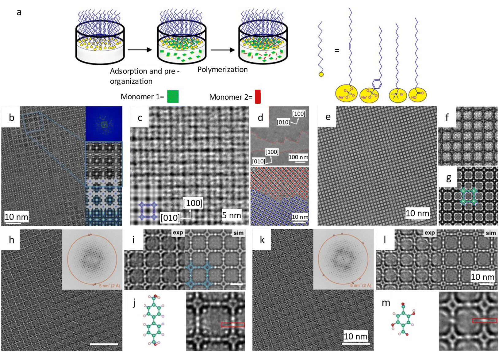
Liu et al.194 reported a surfactant-assisted interfacial strategy to synthesize layered 2D polymers with tunable crystal domains by using surfactants (Fig. 15a). It resulted in a significant enhancement in crystallinity domains from 0.3 μm2 to 121 μm2. HRTEM images in Fig. 15c and d revealed distinct domain boundaries along the (100) and (010) crystallographic planes, as well as tilt and overlapping boundaries. Furthermore, they expanded the on-water surface synthesis approach to construct 2D COFs by the irreversible Katritzky reaction to enhance diversity and stability.195 With a controllable thickness of 2–30 nm, the size of crystalline domains could be enlarged from tens of nanometers to 120 μm2. HRTEM images in Fig. 15b at a dose of 70 e Å−2 revealed a square unit cell with AA stacking, consistent with the predications of modeling simulations. The layered 2D COFs synthesized via the surfactant-assisted interfacial strategy provided an ideal platform for analyzing defects in the pristine framework. The HRTEM Images at a dose of 100 e Å−2 revealed a “micro-flowers” structure composed of grains with distinguishable sizes and orientations.196 A thorough examination of the defects in Fig. 15e–g revealed that antiphase boundaries arise from the oriented attachment of crystalline particles, and can be eliminated through a self-correcting process. Grain boundaries with a tilt angle <10° produce a dislocation array, while maintaining the covalent connection between adjacent grains. Grain boundaries with high tilt angles, on the other hand, result in the termination of building blocks due to geometric prohibition of the covalent bond. Furthermore, rupture occurs along the boundaries under a micromanipulator force, indicating that these defects dominate the mechanical strength of 2D COFs. Recently, these 2D COFs were employed to optimize acceleration voltage.197 Increasing the acceleration voltage, according to classical theory, can reduce radiolysis by decreasing the inelastic scattering cross section. However, this may result in a lower ratio between elastic and inelastic scattering cross sections, indicating a reduction in the elastic scattering cross section, particularly for thin nanosheets exposed to an excess dose. To evaluate the influence of critical fluence and efficiency of electron consumption on resolution, researchers defined an ‘information coefficient’. Simulation results demonstrated a substantial improvement in image contrast, ranging from 41% to 113%, when employing an accelerated voltage of 120 kV. Experimental findings in Fig. 15h–m at 120 kV validated the simulations, showing reduced contrast delocalization and a maximum resolution of 1.9 Å. Interestingly, these results surpassed those obtained at 300 kV, despite occasional aberrant contrast caused by elusive sample structural characteristics.
 | ||
| Fig. 15 Synthesis and low-dose HRTEM characterization of 2D COFs. (a) Schematic illustration of the synthesis of 2D COFs by interfacial reaction. Reproduced with permission.194 Copyright 2019, Springer Nature. (b) Wiener-denoised image of C2DP-Por. Inset: Fourier transform, magnified image, and simulated image (from top to bottom). Reproduced with permission.195 Copyright 2021, Springer Nature. (c) Image of 2DPI. Inset: Simulated image and structural model. (d) Image of two crystalline domains with marked edges (top), and image of a tilt grain boundary with marked core position. Reproduced with permission.194 Copyright 2019, Springer Nature. (e) Raw image, (f) magnified image, and (g) simulated image of L-2D-PI. Reproduced with permission.196 Copyright 2020, American Association for the Advancement of Science. (h) Raw image, (i) magnified image, simulated image, and (j) structural model of linkers and real-space averaged image of 2D-PI-BPDA. (k) Raw image, (l) magnified image, simulated image, and (m) structural model of linkers and real-space averaged image of 2D-PI-BPDA. Reproduced with permission.197 Copyright 2022, Springer Nature. | ||
Like the extensively studied liquid–gas interface, the solid–liquid interface also exhibits great potential as a suitable platform. Cao et al.200 synthesized a crystalline 2D COF membrane through condensing monomers at the interface of a SiO2/Si substrate and precursor solutions. HRTEM images acquired perpendicular to the membrane exhibit highly ordered hexagonal channels with a size of 3.2 nm, indicating the preferred stacking direction of the COF layers. Nanofluidic devices fabricated using these 2D COF membranes exhibited 2–3 orders of magnitude larger ion currents compared to traditional single-channel devices, owing to the massive and ordered channels with charge and electrolyte concentrations of 0.01 M.
Feriante et al.201 employed HRTEM to examine COFs after a reaction time of one minute. The results revealed that COFs were highly crystalline sheets with a thickness ranging from 3 to 30 nm, consistent with the XRD findings. These results indicated that the self-correction of amorphous polymers into an ordered framework may not be a universal way of synthesizing COFs. Instead, it is possible that imine-linked COFs may initially generate ordered sheets with limited registry, which then structurally reorient and stack to construct a COF with three-dimensional order.
The host–guest interaction may also lead to an intriguing degree of polymorphism in switchable DUT-8 (Ni), which can adopt a degenerate family of disorganized configurations.203 The complicated disordered structure arises from six potential up/down interactions between the step-like linker and paddle wheel clusters, which are necessary to meet the boundary requirement. The diffraction patterns suggest the widespread occurrence of stacking faults in the framework and the coexistence of numerous domains inside an individual nanocrystal. It is feasible to switch between well-defined disordered configurations by regularly switching guests to promote the reorientation of the framework, suggesting that it is conceivable to record complicated information pertaining to their physical characteristics by manipulating disordered configurations.
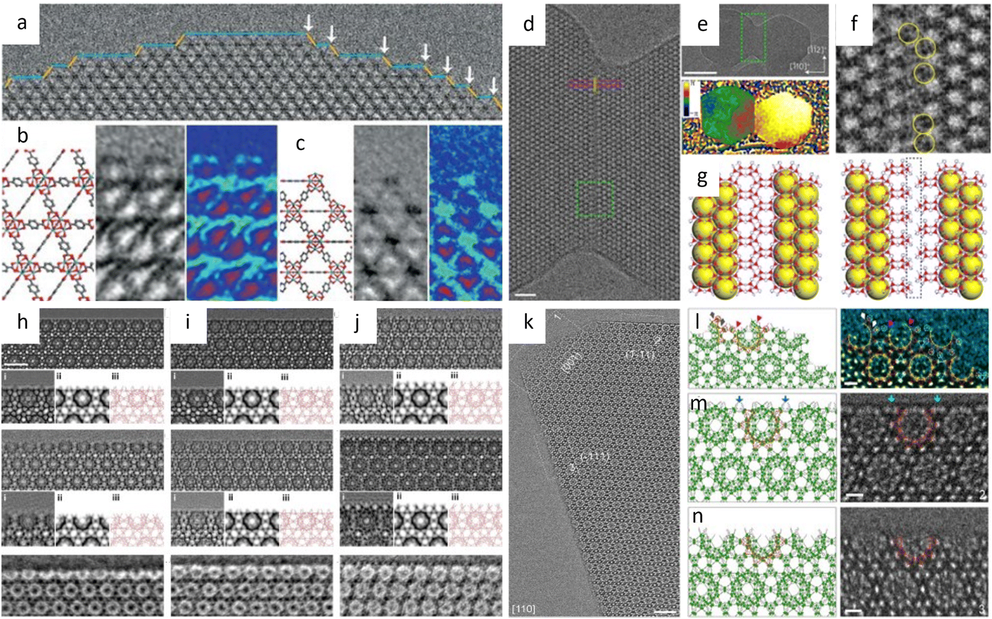 | ||
| Fig. 16 Low-dose image of the surface and interface of MOFs. (a) The terminal steps of UiO-66 including the {100} (blue) and {111} facet (yellow). (b) Structural model, real-space averaged image, and colored image (from left to right) of the ligand-terminated {111} surface. (c) Structural model, real-space averaged image, and colored image (from left to right) of the ligand-free {100}/{111} surface. Reproduced with permission.41 Copyright 2018, The American Association for the Advancement of Science. (d) Enlarged image of the green region in (e). (e) Low-magnification image of the interface (top) and the corresponding geometric phase map in temperature colour codes (bottom) of two ZIF-8 crystals. (f) CTF-corrected image of the green area in (d). (g) Bulk (left) and optimized interfacial structures (right) projected along the [111] direction. Reproduced with permission.25 Copyright 2017, Springer Nature. (h)–(j) CTF-corrected image of fresh MIL-101-HF, MIL-101-NA, and MIL-101-Ac (TOP). CTF-corrected image of vacuum-heated MIL-101-HF, MIL-101-NA, and MIL-101-Ac (middle), and iDPC-STEM image of vacuum-heated MIL-101-HF, MIL-101-NA, and MIL-101-Ac (bottom). (i) Real-space averaged image, (ii) simulated projected potential map, and (iii) structural model. Reproduced with permission.198 Copyright 2019, American Chemical Society. (k) Drift-corrected image of MIL-101 along the [110] direction. (l) Structural model (left) and colored Gaussian-filtered image (right). (m) and (n) Structural model (left) and unfiltered image (right) of the terminal surface structure of MIL-101 with different completeness. Reproduced with permission.199 Copyright 2020, Wiley-VCH GmbH. | ||
The analysis is expanded to another well-studied MOF, MIL-101 (Cr), to determine the effect of additives on the crystallization process, which can improve the crystal size management and/or increase product output.198 Completeness, defined as the proportion of residual hybrid super-tetrahedra in the incomplete medium cage, was used to evaluate the impact of different additives. HRTEM images in Fig. 16h–j obtained at 8 e Å−2 revealed uniform {111} surfaces terminated by almost medium cages with varying degrees of completeness. MIL-101 synthesized with no additives or with HF exhibited the same open surface completeness of 80%, while the samples from acetic acid showed 100% completeness. This is the first time that the impact of additives on the surface structure has been measured. Han et al.199 also observed a similar phenomenon involving incomplete cages at the surface, specifically the loss of one or two Cr3(μ3-O) at the smooth terminal (11) surface (Fig. 16k–n). The (11) facets exhibited an unusually uneven surface, which may be the consequence of a distinct loss model for the three trimers at the sublayer surface. The transition from a sublayer surface to a stable top surface suggested a possible crystal growth mechanism, which involved the progressive formation of full super-tetrahedra through the attachment of Cr3(μ3-O) trimers.
Low-dose TEM has emerged as the predominant method for atomic imaging of COMs. Nonetheless, the application of TEM encounters certain limitations. For example, the CTF in TEM images varies dramatically with defocus, necessitating precise defocus measurement for reliable image interpretation. Second, the implementation of spectroscopic techniques such as EELS and EDS to obtain atom-specific information, including species identification and valence states, is more intricate in the TEM model. Consequently, there is a growing exploration of STEM as an alternative approach to achieve interpretable images with higher resolution, as well as for spectroscopic analyses.
4.2 STEM
The iDPC-STEM method (Fig. 17a) has become a prevalent strategy for characterizing beam-sensitive materials, such as perovskites,211 zeolites,54 and MOFs/COFs, owing to its high electron utilization efficiency and high SNR. Shen et al.212 applied the iDPC-STEM imaging technique to reveal the atomic structure of MIL-101 and applied it to beam-sensitive materials including MOF UiO-66 and zeolites ZSM-5 and SAPO-34. The traditional ADF-STEM imaging method can only demonstrate the ordered spheres and lattices of MIL-101, but it is unable to differentiate between node–linker coordination. Intriguingly, the averaged iDPC-STEM images in Fig. 17b–d at a beam current of less than 0.1 pA can reveal the node–linker coordination, which consists of three 1,4-benzene dicarboxylate linkers in each coordination with high contrast. Additionally, the spatial resolution of 4.7 Å provided sufficient details, although the determination of individual atoms remains challenging.27 The iDPC-STEM method was also used to investigate the microstructure of BZIF-8 composites, which exhibit unexpected activity when the pore size of BZIF-8 is smaller than the enzymatic substrate.40 The iDPC-STEM images in Fig. 18i and j of BZIF-8-S revealed that the 12 Å periodic cavity with pore sizes of 3.4 and 2.8 Å is formed by Zn clusters and 2-methylimidazole, respectively. In contrast, BZIF-8-B exhibited co-existence of crystalline and amorphous phases with feeble diffraction intensity. Furthermore, the disordered structure exhibited numerous coordination defects, which accounted for the high enzyme activity. Additionally, an intriguing phase transformation from an initial SOD-type to a dia-type nanosheet was discovered in BZIF-8-B, whereas this transformation was absent in BZIF-8-S.
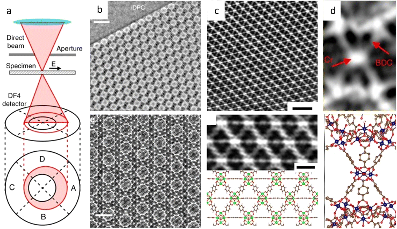 | ||
| Fig. 17 The schematic illustration and imaging of iDPC-STEM. (a) The workflow of iDPC-STEM: four images detected by the segments of the DPC detector can be calculated to DPCx and DPCy, which can be further integrated into the iDPC-STEM image. (b) iDPC-STEM image integrated from the DPC image (top, scale bar: 10 nm), and magnified image (bottom, scale bar: 5 nm). (c) Image of UiO-66 along the [100] direction (top), and magnified image with the structural model (bottom). Scale bar: 3 nm. (d) Imaging of super tetrahedra in MIL-101 constructed by Cr and the organic linker (top) and the structural model (bottom). Reproduced with permission.212 Copyright 2020, Springer Nature. | ||
STEM images for UiO-66 indicated that the structure of the two sides of the interface exhibited significant difference.145 The core area showed three Zr clusters, while the shell region showed six. Additionally, huge clusters were hexagonally organized with a P6mm projection. The data could then be used to reconstruct a 3D potential map, which revealed the connection of the Zr12 cluster with 12 other clusters. As a comparison, HAADF-STEM images showed an arrangement of indistinct ZrO nodes without linkers, DPC-STEM images showed linkers vaguely present with obvious noise, and iDPC-STEM images showed clear Zr–O nodes and linkers (Fig. 18a–d).44
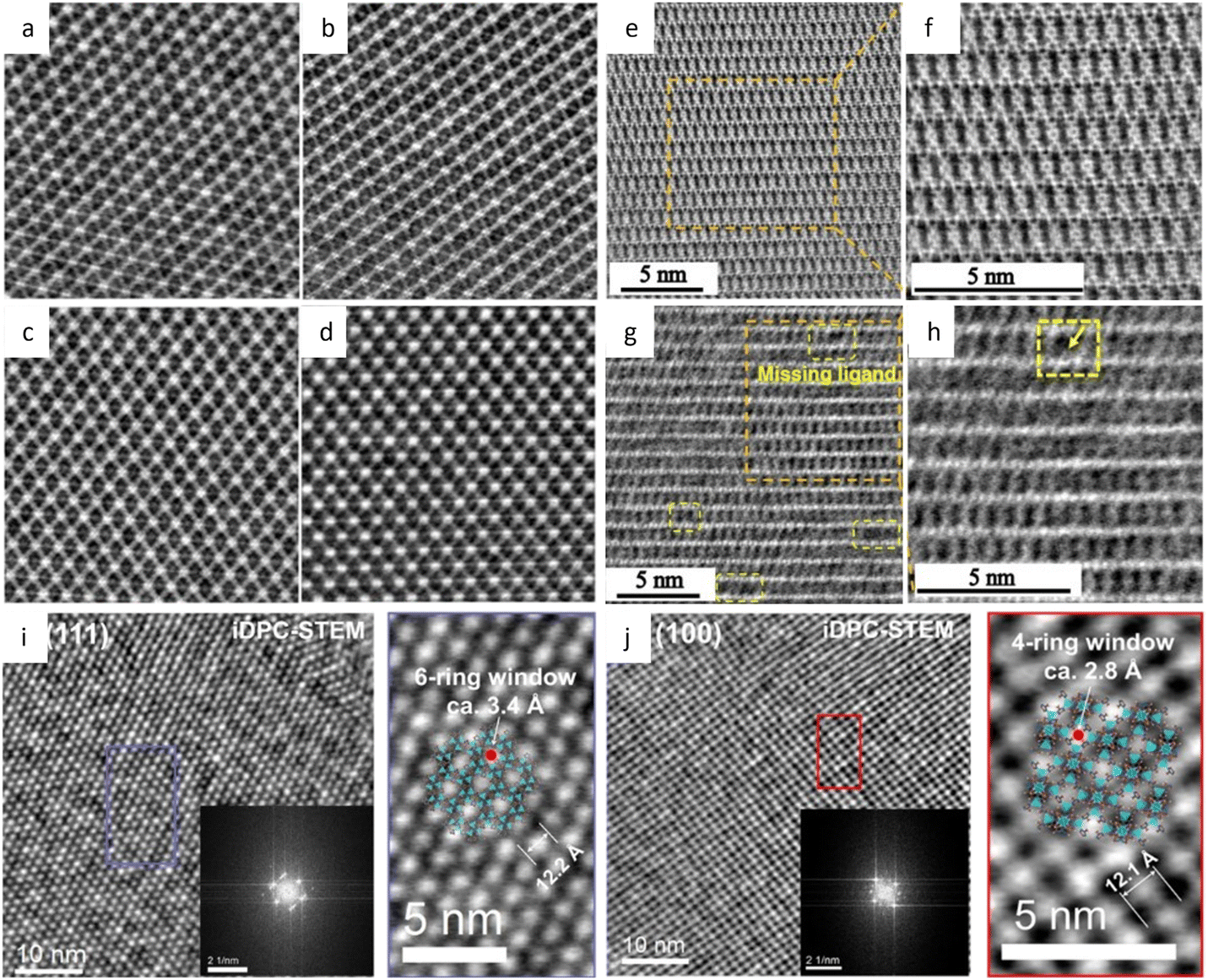 | ||
| Fig. 18 The iDPC-STEM characterization of MOFs. (a)–(d) Image of UiO-66 (Zr) along the [110] direction with different dwell time: 8, 16, 32, and 64 μs, respectively. Reproduced with permission.44 Copyright 2023, American Chemical Society. (e) High-magnification image and (f) magnified image of Ni-BDC-T. (g) High-magnification image and (h) magnified image of FeNi-BA-T with missing ligand defect. Reproduced with permission.214 Copyright 2022, Wiley-VCH GmbH. (i, j) Image of BZIF-8-S along (i) the [111] direction and (j) the [100] direction. Reproduced with permission.40 Copyright 2022, Springer Nature. | ||
Feng et al.213 synthesized bimetallic (Zn,Zr)-UiO-66 with easily removable Zn nodes to construct a crystal with cluster defects. The iDPC-STEM images along the (100) direction revealed an obvious absence of clusters, resulting in a topology switch from fcu to reo net. UiO-66 with four defects/clusters demonstrated a considerable increase in styrene oxide conversion from 17% to 90%, and a twofold improvement in CO2/N2 selectivity. Sun and colleagues214 incorporated Fe3+ into the skeleton of Ni-MOF to create multivariate MOFs with varying lattice strain for enhancing the electrocatalytic ability. STEM images in Fig. 18e–h showed numerous missing ligand defects in the thermally treated sample FeNi-BA-T, whereas the original Ni-MOFs exhibited no evident defects. FeNi-BA-T exhibited superior oxygen evolution reaction activity compared to that of commercial RuO2, due to the unsaturated metal atoms at the defects and the reduced lattice strain variation. To investigate the effects of functionalization on the dynamic properties, Liu et al.215 analysed the rotation properties of BDC linkers to establish a correlation between linker structure and local rigidity. Notably, the intensity profile along the long axis revealed an intriguing trend in the width of the projection of BDC-X linkers, wherein the signal of BDC-NH2 transformed from a narrow line with a full width at half maximum of 2.01 Å to a broader spot measured as 4.02 Å in BDC-Br. This broadening phenomenon indicated the π-flipping of benzene rings induced by different functional groups, supporting the trend of –OH > –NH2 > –H > –CH3 ∼ –F > –Cl > –Br. Subsequently, the most rigid UiO-66-OH exhibited the highest CO2 adsorption capacity, confirming the advantageous effect of rigidity on the adsorption of guest molecules.
Zhang et al.216 incorporated tetra-topic chromophores into the skeleton of COFs to enhance two-photon absorption performance. The iDPC-STEM images revealed an offset distance between layers of 0.4 nm, consistent with the value of 1/8 a offset along the a axis. The micrometer-sized COF-606 single crystals with serrated interlayer stacking exhibited the highest two-photon action cross-section value. Liu et al.217 synthesized topological isomers JUC-620 with a dia net and JUC-621 with a qtz net by calculating the potential energy. The iDPC-STEM images along the [100] direction of JUC-621 revealed the symmetry type of p2mm that matched well with the simulated projective potential. The space group symmetry was further determined as P6422. Combined with cryo-FIB, iDPC-STEM images facilitated the observation of core–shell structures in MOF-COF with a sharp boundary.146 The application of this combined approach allowed for the precise characterization of the interpenetrated structure of MOF-5 and the half hexagonal-shaped channel at the interface.
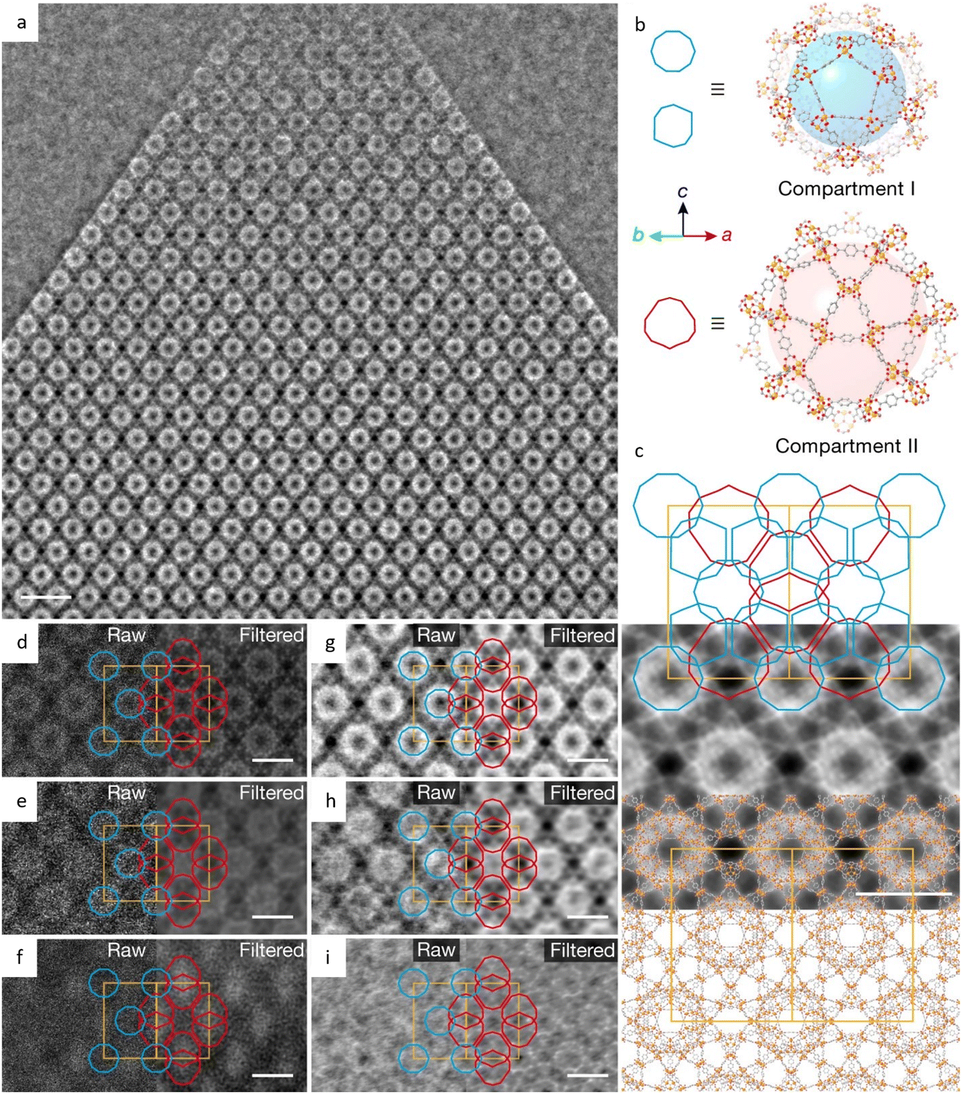 | ||
| Fig. 19 The observation of the guest molecule in MOFs by the iDPC-STEM image. (a) Image of MIL-101-Cr along the [110] direction. Scale bar: 10 nm. (b) Two structural models (compartments I and II) with specific position of guest TiO2. (c) Symmetry-imposed image overlaid with the pore distribution map (top) and the structural model (bottom). (d)–(f) Raw and filtered HAADF image, and (g)–(i) raw and filtered iDPC-STEM image overlaid with the pore distribution map. Scale bar: 5 nm. Reproduced with permission.218 Copyright 2020, Springer Nature. | ||
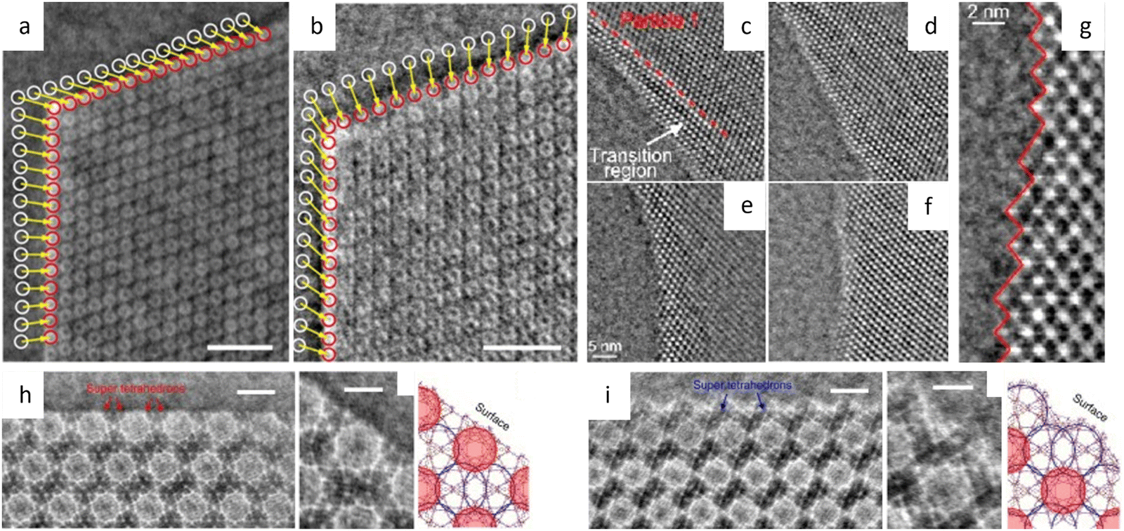 | ||
| Fig. 20 The terminal surface structure observation by iDPC-STEM. (a, b) Image of the MIL-101 surface (a) before and (b) after electron irradiation. Reproduced with permission.27 Copyright 2020, American Chemical Society. (c)–(f) Images with continuous transition area and (g) magnified image of the jagged surface of UiO-66 (Zr). Reproduced with permission.220 Copyright 2020, American Chemical Society. (h) and (i) Two types of terminal surface image (left, scale bar: 5 nm), magnified image (middle, scale bar: 3 nm), and structural model (right) of MIL-101. Reproduced with permission.212 Copyright 2020, Springer Nature. | ||
The interface analysis of two identically oriented UiO-66 crystals revealed a continuous lattice at the transition region with an irregular terminal mode (Fig. 20c–g). In contrast, the interface analysis of two crystals with different orientations revealed chemical bonding between metal nodes and organic linkers with a distortion of the node.220 The coordination formed through periodically arranged organic linkers suspended outside of the metal was confirmed by the intensity profile analysis.
The iDPC-STEM method has achieved notable success in the high SNR visualization of heavy and light atoms within the COM structure. However, this method necessitates precise zone axis alignment and specific defocus settings to obtain clear and interpretable images, resulting in a relatively low success rate. Consequently, in addition to the combination with auto-alignment techniques, emerging technologies such as ptychography by 4D-STEM have been employed to address the challenges associated with imaging beam-sensitive materials.
5. Upcoming approaches and techniques
Over the past few decades, low-dose TEM/STEM have progressively become routine imaging techniques for elucidating the local structure, host–guest interaction, and surface of extremely sensitive COMs. These techniques advance the comprehension of the structure–property relationship to guide the design of specific materials with prospective functions. However, HRTEM imaging is constrained by CTF and requires a precisely determined defocus value, HAADF-STEM imaging is insensitive to light atoms in organic linkages, and iDPC-STEM imaging requires precise focusing. Further development is required for optimisation of image acquisition conditions to minimize excess dose consumption, and post-processing to eradicate noise or extract structural information for an ideal SNR. The novel imaging mode, known as 4D-STEM, holds great promise as a highly effective technique for low-dose imaging. By capturing massive information from both real and reciprocal space and leveraging redundancy in the data, 4D-STEM enables the recovery of high-quality images. Pioneering work conducted by Peng et al.208 utilizing the ptychography algorithm demonstrated the successful recovery of the MOF structure using 4D-STEM. However, additional tuning and careful selection of the ptychography algorithm are necessary to achieve an ideal reconstruction at minimal dose. These developments may also shed light on the incorporation of in situ technology, a potent method for performing real-time intuitive imaging under different stimuli, which enables direct imaging of the dynamic process of catalysis and reveals the dynamic interactions of reactant molecules with the active site, even for the beam-sensitive materials. 4D-STEM and in situ techniques have revolutionized the acquisition of extensive spatiotemporal data, offering unprecedented insights into material behavior. The advancements in these techniques owe much to the progress in computer science, which has facilitated the processing and analysis of the vast amount of data generated. In recent years, machine learning (ML), an advanced and innovative technology, has witnessed remarkable progress in its application to electron microscopy, specifically in the domains of imaging and spectroscopy.221 Despite the significant advancements achieved thus far, the full potential of ML in TEM and STEM is yet to be fully realized. This can be attributed to the rapid evolution of ML algorithms, the wealth of data generated by direct electron detectors, and the inherent complexity of specimen structures.5.1 Ptychography by 4D-STEM
The 4D-STEM dataset consists of a series of CBED patterns generated at each scan position. These patterns contain voluminous structure information that can be used for reconstruction by various algorithms, such as ADF and BF images using virtual detectors, center of mass images analogous to DPC and iDPC images, and ptychographic phase images. Among these algorithms, ptychography can generate interpretable phase images, allowing for simultaneous imaging of heavy and light atoms. Additionally, it permits scanning by defocused beams, which improves dose efficiency and data acquisition rate. Furthermore, it has a higher thickness tolerance due to the flexibility in adjusting the scanning region and sampling method. Therefore, ptychography has been applied to various materials, including 2D materials and biological samples.Ptychographic phase images of mono-layered MoS2 revealed much more distinguishable atoms than those in HAADF images acquired at a similar dose.222 Atomic-resolution images with a resolution of 1.58 Å were also reconstructed at a dose of 403 e Å−2. Jiang et al.58 reconstructed a series of images of mono-layer MoS2 at a range of doses from 250 to 2000 e Å−2 using a distinct algorithm. The image quality clearly improved as the dose increased. The information limit of full-field ptychography images was 5α, corresponding to an Abbe diffraction-limited resolution of 0.39 Å, which is substantially lower than that of conventional ADF (0.98 Å). Using a mixed quantum state to describe the partial coherence, mixed-state ptychography223 was proposed to reconstruct the images of bilayer MoSe2/WS2.224 The lattice can be discerned even at a dose of 375 e Å−2 in Fig. 21e–j. Zhou et al.225 combined cryo-TEM with ptychography to analyse the biological rotavirus and non-symmetric immature particles at a low dose of 5.7 e Å−2. The combination of these two techniques demonstrated high-quantity reconstruction with substantially enhanced contrast transfer and phase sensitivity, yielding high-quality data with wider and continuous CTF. The superiority of ptychography reconstruction was further demonstrated by the 3D phase reconstruction of organic DNA with inorganic Au particles,226 and single particle analysis with a wide bandwidth for small molecules such as rotavirus double-layered viral particles.227
The high-quality reconstruction of biological specimens by ptychography offers the potential for elucidating beam-sensitive materials such as zeolites, despite the challenges posed by the need for atomic imaging and zone axis alignment. O'Leary et al.228 proposed a strategy for reducing the exposure duration of the specimen by altering the bit depth of the detector. Using this method, the atomic structure of ZSM-5 can be revealed at a dose of 200 e Å−2, despite the ambiguity of the thinner region due to insufficient scattering. Dong et al.229 disclosed the local structure of Na+ ion occupied zeolite LTA and guest-containing ZSM-5 using ptychography with the iterative ePIE at a dose of less than 3000 e Å−2 (Fig. 21a–d). They also demonstrated that the iterative technique can achieve a higher resolution reconstruction than the non-iterative technique.
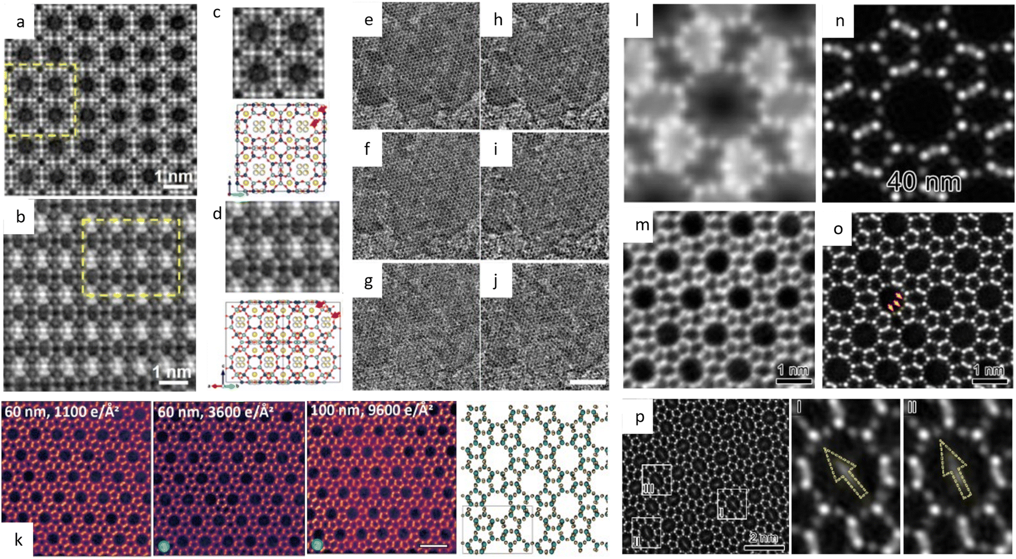 | ||
| Fig. 21 Ptychograpghy reconstruction of zeolite and 2D materials based on the 4D-STEM dataset. (a) Reconstructed image, and (c) magnified image and structural model of the Na-LTA zeolite along the [100] direction. (b) Reconstructed image, and (d) magnified image and structural model of the Na-LTA zeolite along the [110] direction. Reproduced with permission.229 Copyright 2023, American Chemical Society. (e)–(j) Mixed-state ptychography reconstruction of WS2 at a total dose of 1500, 790, and 375 e Å−2. (h)–(j) Single-state ptychography reconstruction of WS2 at a total dose of 1500, 790, and 375 e Å−2. Scale bar: 3 nm. Reproduced with permission.224 Copyright 2020, Springer Nature. (k) Low-magnification image (scale bar: 100 nm) and (m) ptychography reconstructed images and structural model of ZSM-5. Scale bars: 5 nm. Reproduced with permission.230 Copyright 2023, American Association for the Advancement of Science. (l) and (m) Simulated and experimental iDPC-STEM images, and (n) and (o) ptychography images of ZSM-5 of 40 nm. (p) Ptychograpghy images of ZSM-5 with adsorbed p-xylene molecules. Reproduced with permission.231 Copyright 2023, The American Association for the Advancement of Science. | ||
To overcome the time-consuming zone axis alignment process, Sha et al.232 developed a method that makes the Fresnel propagator adaptive to eliminate the misalignment. They applied the proposed method to imaging ZSM-5 with a thickness of 60 nm at a dose of 1100 e Å−2, which revealed deformation along the lateral and depth directions due to the structure's flexibility, as well as dose-dependent visibility of individual metal atoms in the pores (Fig. 21k).230 In a recent study by Zhang et al.,231 the potential of ptychography in reconstructing the projection direction was realized, enabling the identification of 3D inhomogeneities within the zeolite structure (Fig. 21l–p). Through the reconstruction of a ∼40 nm-thick specimen, the presence of oxygen was unambiguously identified, which was previously achievable only in the case of iDPC-STEM when the sample thickness was below 12 nm. The reconstructed ptychographic image exhibited excellent contrast, facilitating the identification of adsorbed p-xylene molecules, and enabling direct observation of oxygen vacancies within the zeolite framework. Moreover, the depth-resolution was determined to be approximately 6.6 nm by analyzing the intensity profile using derivative curves along two atomic columns in seven slices. This approach demonstrated 3D imaging with a high dose-efficiency compared to other methods such as electron tomography and optical sectioning.
However, exceedingly sensitive MOF/COF materials are rarely explored. Simulation results of UiO-66 demonstrated that the reconstructed images matched the crystal structure nearly identically even though data were acquired with a large defocus value of 100 nm.233 However, implementing it in practice remains difficult. Recently, Peng et al.208 used ptychographic reconstruction to analyse the structure of an ultra-thin metal–organic layer in which individual Hf clusters were discernible at a transfer of information of 1/2.36 Å−1. The images simultaneously displayed metal clusters with six organic linkers, corresponding well with the simulated images of four-layer metal–organic layers. Notably, the total dose for the acquisition of the dataset is 864 e Å−1, significantly higher than most doses used in low-dose HRTEM/STEM. This indicates that additional investigation is required to determine the universality of 4D-STEM characterization in ultra-sensitive materials.
Ptychography has demonstrated the ability to image beam-sensitive biological specimens and zeolites at a comparatively low dose. However, the realistic dose for atomic-resolution reconstruction typically ranges from several hundreds to thousands, which is higher than that used for imaging exceedingly beam-sensitive materials such as MOFs and COFs. Therefore, the application of ptychography to these exceedingly delicate substances requires further investigation.
5.2 In situ techniques at atomic resolution
In situ TEM/STEM techniques, conducted under a single or multiple stimuli introduced into the specimen chamber, allow for the mimic of realistic scenarios. These techniques enable observation of the structural evolutions of materials in real time, facilitating a comprehensive understanding of the dynamic structure–property relationship. The development of in situ techniques has enabled the introduction of stimuli that encompass most application sectors for materials, including crystal growth, structure evolution, chemical catalysis, and electrocatalysis, among others. For example, the growth of Pt nanocrystals at the atomic level was monitored in liquid cells by TEM.234 It revealed that the growth rate of all facets at small size suffers a block in (100) facets as the crystals grow up, leading to an understanding of the mechanisms of crystal growth and shape formation. Yuan et al.235 visualized the dissociation and reaction of adsorbed water molecules through a twin-protrusion structure on the (001) surface of TiO2 at 700 °C. Sun and co-workers236 observed the formation and behaviour of mismatch dislocations during the transformation of Cu2O/Cu at the interface when H2 flow was introduced at 873 K. However, due to the complexity of the system and chamber design, in situ research at the atomic level on photo/electro-catalysis is typically not achieved.In situ characterization requires a long-term observation and is conducted at the lowest possible dose rate (on the order of 100 e Å−2 s−1) to avoid beam-introduced error. However, this dose is still significantly higher than the critical threshold for beam-sensitive materials. Fortunately, the low-dose technique has been developed and applied to monitor crystal growth, structural transformation and catalysis of MOFs and COFs. Patterson et al.237 reported a real-time observation of the growth of a ZIF-8 crystal at a dose rate of 15 e Å−2 s−1 within 11 min. This observation revealed that the nucleation can be constrained by the local depletion of monomers, providing insights into the mechanisms underlying crystal growth. Additionally, this study represents the first observation of the growth of beam-sensitive materials, demonstrating the potential for in situ techniques. In situ techniques have been employed to visualize the growth of 1D MOF nanotubes238 and colloidal COFs239 at modest fluxes of 0.05 e Å−2 s−1 and 0.66 e Å−2 s−1 respectively. At an ultra-dose rate of 0.04 e Å−2 s−1, Parent and co-workers240 observed pore breathing behavior in MIL-53(Cr) in response to water adsorption and temperature variations. In situ observation of a phase transition from NU-906 to NU-1008 at an accumulated dose of 6 e Å−2 s−1 was also achieved by acquiring images every few minutes.241 However, all of these in situ observations were conducted on a microscale rather than an atomic scale, highlighting the need for further advancements to extend low-dose atomic imaging from ex situ to in situ.
5.3 Machine learning
In recent years, machine learning has emerged as a powerful tool with applications spanning various scientific disciplines. Notably, in the context of electron microscopy, ML has demonstrated considerable potential in image denoising and phase retrieval discussed in Section 3. The utilization of supervised and unsupervised ML techniques has enabled efficient processing of data, leading to improved results in a time-effective manner. Furthermore, the advent of emerging techniques such as 4D-STEM and in situ technologies has resulted in the generation of massive datasets, necessitating advanced computer science methodologies for the extraction and analysis of relevant information. In this regard, ML offers new opportunities for achieving rapid and accurate results in the analysis of these complex datasets.ML has been utilized in denoising using diverse strategies since the first application of neural networks in image denoising in 1989. Auto-encoding neural networks have shown the ability to reconstruct images with over 90% accuracy of column position after training with thousands of random sample images, along with improved contrast variation.242 To realize a time-effective and fully informative recovery, convolutional neural networks (CNNs) advanced by graphical progressing unit (GPU) acceleration are being employed for assembling high-quality images without the blurring effect within an appropriate timescale.243 Unlike the conventional convolution process, the divided pointwise and depthwise convolutions work more effectively, ensuring outstanding performance in suppressing noise. Practice using the sample datasets generated from multislice image simulation exhibited outstanding performance in presenting nonperiodic defects at ultra-low SNR. This demonstrated that the network can take advantage of both overall and localized information during the noise determination, and allows one to flexibly adjust the filtering strategy in the presence of atomic defects.244 Additionally, a method to determine the consistency between the denoised images and original information was also proposed.245 Another unsupervised method, K-means clustering, was applied to binarize the atom column and background for specifying the center of mass fitting zone.246 The dominant Poisson noise can be eliminated through integration of Anscombe transform, block matching and 3D filtering, histogram stretching, and morphology filtering. The average error in the images is less than 0.7 pixel with an increased SNR to 7 to 11 dB, as well as an enhancement in the signals of light atoms.
The revolution in ptychography is accompanied with the development of pixel array detectors in 4D-STEM.247 4D-STEM generates multidimensional datasets including full information of the specimen, which is theoretically perfect for reconstruction. However, a comprehensive and efficient analysis remains challenging for the massive amount of data. It is difficult to explicate the nonlinear relationship between acquired signals and inherent properties in a linear way. Based on linear decomposition, the artifacts in raw diffraction patterns can be eliminated.248 Furthermore, by evaluating the metaparameters, the amount of data can be reduced by up to 68-fold compared to the original data with a suitable cut-off. By combining variational autoencoders with rotational symmetry, a succinct presentation of 4D-STEM data with an atomic visualization of the symmetry-breaking map was achieved.249 Even a single atom or vacancy in monolayer graphene can be identified, which might help to determine the abnormality even with a small atomic difference. Manifold learning, another nonlinear method in ML used to identify the underlying relation, has been utilized to approximate the nearest adjacent image in order to solve low-dimensional signals and iteratively reconstruct them.250 This technique can extract multidimensional underlying information even from the weak diffraction pattern obtained from monolayer graphene, demonstrating the potential for low dose imaging and holonomic signal analysis. One such development is the work of Friedrich and colleagues,251 who developed a network to retrieve a complex wave and recover images using CNNs based on the phase objective approximation and neighbouring diffraction patterns. This approach allows for rapid predictions in almost real-time, while the resulting images exhibit high SNR, high spatial resolution, and simultaneous imaging of both light and heavy atoms at comparable low electron dose.
In situ technology holds the potential to provide real-time observations of inner reaction mechanisms. However, the vast amount of data generated, ranging from tens to hundreds of images per minute, poses significant challenges for traditional processing methods. In this context, machine learning techniques based on mathematical models demonstrate great promise for the automatic processing of data with high efficiency and accuracy. Fully connected neural networks (FCN) based on an encoder–decoder architecture have proven effective in extracting features from in situ STEM datasets.252 Through training, these networks can automatically capture high-resolution atomic relationships and structural information related to chemical bonding, such as the dynamic switching between different coordination states of silicon dopants in graphene over time. The weakly supervised FCN model trained on simulated STEM images enables quantitative analysis of each frame of high-dimensional in situ STEM data with minimal manual intervention, facilitating the self-adjustment of the microscope settings. Lee et al.253 provide a practical guide for training deep learning models for the determination of vacancies and polymorph types, showcasing the accuracy of FCN models on a substantial number of experimental STEM images, which is comparable to meticulous manual analysis. On the other hand, the U-Net neural network, unlike FCN, incorporates skip connections to preserve context and details more effectively. Its smaller parameter count makes it particularly suitable for challenging datasets such as STEM images, where obtaining data annotations can be difficult. Yao et al.254 pioneered the application of U-Net in the analysis of liquid-phase TEM images, revealing valuable information about reaction kinetics and assembly dynamics. The U-Net model showcased its capability in predicting the position and shape boundaries of nanoparticles amidst highly noisy and fluctuating backgrounds, thereby uncovering properties such as the anisotropic interaction landscape of nanoprisms. Lu et al.255 successfully employed the U-Net architecture to identify all Pt–Ni nanoparticles in a case study involving bimetallic Pt–Ni catalyst nanoparticles, effectively segmenting them by well-defined outlines with much higher accuracy of edge detection. U-Net has demonstrated remarkable capabilities even in identifying seemingly unremarkable features, such as nanopores, in nanopore-healing images during investigating the healing behavior of magnetic 1T-CrTe2.256 Through the application of U-Net, the automatic identification of nanopores was achieved, showcasing the network's ability to accurately discern and analyze subtle details in the healing process.
The rapid development of ML has provided unprecedented capacity for electron microscopy, enabling the complex and time-consuming analysis process. This has vastly enhanced the analysis efficiency and accuracy. However, the success rate of ML under low-dose conditions endures an untenable decrease during the analysis due to the low SNR. This indicates that a further modification in ML is required for an accurate determination of beam-sensitive materials.
6. Summary and outlook
In recent decades, the development of MOFs and COFs, two crystalline porous frameworks, has led to widespread applications in various fields due to their high surface area, facilely tailored functionality, and designable pore structure. The MOFs/COFs' flexible organic linkages bestow them with diverse synthesis strategies, chemical structures, and topologies, making them ideal platforms for studying the structure–property relationship. However, the organic components of MOFs/COFs are sensitive to irradiation, making it difficult to determine the atomic structure using conventional TEM/STEM techniques. Recently, the low-dose technique has been swiftly developed for beam-sensitive materials, becoming a promising technique for imaging MOFs/COFs. These advancements rely on the integration of multiple technologies:i. The development of DEDs enabled high-quality imaging with improved spatial resolution under low-dose conditions. Segmented detectors enabled integration of the fully recorded scattered electron with spatial distribution, which is the foundation for the newly developed iDPC-STEM to reconstruct phase images. The pixelated detector enables the recording of the entire spectrum of reciprocal space information, accelerating the acquisition of 4D-STEM datasets by recording CBED at each position for post-processing techniques such as ptychography. When specialized ‘hollow’ DEDs become available, the multimodal STEM mode, incorporating simultaneous imaging techniques (ptychography, HAADF-STEM, and DPC) along with spectroscopy (EDS and EELS), will facilitate comprehensive and reliable investigations into the structure and chemistry at ultrahigh spatial resolution.
ii. Low-dose zone-axis alignment enables automated tilting by a program that can calculate the deviation from the initial electron diffraction pattern, thereby minimizing dose consumption. The combination of sparse sampling and CS can recover all information with a significantly reduced dose consumption.
iii. The denoising of images by advanced algorithms can improve the SNR of acquired images, revealing more embedded information. Phase retrieval can aid in the reconstruction of phase images for interpretable images, in which ptychography can achieve the highest resolution at the same dose as other modes. In addition, simulation software has been developed to predict the image and determine the degree of similarity between experiment and simulation.
iv. The introduction of a cryogenic system to FIB for sample processing can effectively reduce the damage caused by the focused ion beam, and the sample protection by coating can reduce surface sputtering caused by the incident beam.
These developments facilitate the practical application of low-dose techniques, which helps disclose the exact structure of MOFs/COFs from metal clusters to organic linkage at the atomic level, elucidating the local structure, host–guest interaction, and surface and interface structure. These images provide solid evidence to explain the improvement in property from the perspective of microstructure difference, steering the modification and functionalization of materials based on the design of building blocks.
Despite the gratifying advances in low-dose technology, issues remain. A precisely determined defocus value is required for the analysis of HRTEM images, and a precisely focused beam results in a low success rate in iDPC-STEM. Machine learning may provide a solution for the analysis of collected images by identifying features automatically, even if they are indistinguishable to the naked eyes or conventional computer analysis; however, algorithm optimization is still required. In addition, ptychography in 4D-STEM, which can reconstruct the clearest images with the highest resolution near lattice vibrations, has tremendous potential for imaging beam-sensitive materials. While ptychography has been successfully applied to MOFs at a dose of 800 e Å−2, the possibility of imaging at ultra-low dose (<100 e Å−2) requires further investigation, despite the significant improvement in relevant computing capacity. Extremely beam-sensitive materials may necessitate the use of potent algorithms in conjunction with machine learning to accomplish imaging. If achieved, the monitoring of beam-sensitive materials at the atomic level in real time will no longer be an unattainable future objective.
Conflicts of interest
There are no conflicts to declare.Acknowledgements
The authors acknowledge support from startup grant from the Department of Applied Physics, the Hong Kong Polytechnic University (1-BDCM), the General Research Fund (No. 15306021, 15306122), and the Early Career Scheme (No. 25305023) from the Hong Kong Research Grants Council (RGC), and the Warwick Startup Funding.References
- M. Varela, A. R. Lupini, K. V. Benthem, A. Y. Borisevich, M. F. Chisholm, N. Shibata, E. Abe and S. J. Pennycook, Annu. Rev. Mater. Res., 2005, 35, 539–569 CrossRef CAS.
- M. R. Lee, Mineral. Mag., 2018, 74, 1–27 CrossRef.
- S. Abednatanzi, P. G. Derakhshandeh, H. Depauw, F. X. Coudert, H. Vrielinck, P. Van Der Voort and K. Leus, Chem. Soc. Rev., 2019, 48, 2535–2565 RSC.
- O. M. Yaghi, G. Li and H. Li, Nature, 1995, 378, 703–706 CrossRef CAS.
- A. P. Cote, A. I. Benin, N. W. Ockwig, M. O'Keeffe, A. J. Matzger and O. M. Yaghi, Science, 2005, 310, 1166–1170 CrossRef CAS PubMed.
- Y. Cheng, S. J. Datta, S. Zhou, J. Jia, O. Shekhah and M. Eddaoudi, Chem. Soc. Rev., 2022, 51, 8300–8350 RSC.
- S. Yuan, X. Li, J. Zhu, G. Zhang, P. Van Puyvelde and B. Van der Bruggen, Chem. Soc. Rev., 2019, 48, 2665–2681 RSC.
- R. Liu, K. T. Tan, Y. Gong, Y. Chen, Z. Li, S. Xie, T. He, Z. Lu, H. Yang and D. Jiang, Chem. Soc. Rev., 2021, 50, 120–242 RSC.
- G. Chakraborty, I. H. Park, R. Medishetty and J. J. Vittal, Chem. Rev., 2021, 121, 3751–3891 CrossRef CAS PubMed.
- X. Zhao, P. Pachfule and A. Thomas, Chem. Soc. Rev., 2021, 50, 6871–6913 RSC.
- K. Winkler, Chem. Rev., 2022, 122, 10573–10574 CrossRef CAS PubMed.
- P. M. Bhatt, V. Guillerm, S. J. Datta, A. Shkurenko and M. Eddaoudi, Chem, 2020, 6, 1613–1633 CAS.
- K. Geng, T. He, R. Liu, S. Dalapati, K. T. Tan, Z. Li, S. Tao, Y. Gong, Q. Jiang and D. Jiang, Chem. Rev., 2020, 120, 8814–8933 CrossRef CAS PubMed.
- F. Haase and B. V. Lotsch, Chem. Soc. Rev., 2020, 49, 8469–8500 RSC.
- D. B. Williams and C. B. Carter, The transmission electron microscope, Springer, 1996 Search PubMed.
- M. J. Cabral, Z. Chen and X. Liao, Microstructures, 2023, 3, 2023040 CrossRef.
- X. Wang, Y. Q. Wang, Y. C. Feng, D. Wang and L. J. Wan, Chem. Soc. Rev., 2021, 50, 5832–5849 RSC.
- A. Sweetman, N. R. Champness and A. Saywell, Chem. Soc. Rev., 2020, 49, 4189–4202 RSC.
- A. Bogner, P. H. Jouneau, G. Thollet, D. Basset and C. Gauthier, Micron, 2007, 38, 390–401 CrossRef CAS PubMed.
- T. Sun, L. Wei, Y. Chen, Y. Ma and Y. B. Zhang, J. Am. Chem. Soc., 2019, 141, 10962–10966 CrossRef CAS PubMed.
- M. Ge, Y. Wang, F. Carraro, W. Liang, M. Roostaeinia, S. Siahrostami, D. M. Proserpio, C. Doonan, P. Falcaro, H. Zheng, X. Zou and Z. Huang, Angew. Chem., Int. Ed., 2021, 60, 11391–11397 CrossRef CAS PubMed.
- Z. H. Huang, E. S. Grape, J. Li, A. K. Inge and X. D. Zou, Coord. Chem. Rev., 2021, 427, 213583 CrossRef CAS.
- T. Yang, T. Willhammar, H. Xu, X. Zou and Z. Huang, Nat. Protoc., 2022, 17, 2389–2413 CrossRef CAS PubMed.
- X. C. Ren, X. Q. Zhang, R. Xu, J. Q. Huang and Q. Zhang, Adv. Mater., 2020, 32, e1908293 CrossRef PubMed.
- Y. Zhu, J. Ciston, B. Zheng, X. Miao, C. Czarnik, Y. Pan, R. Sougrat, Z. Lai, C. E. Hsiung, K. Yao, I. Pinnau, M. Pan and Y. Han, Nat. Mater., 2017, 16, 532–536 CrossRef CAS PubMed.
- S. Ghosh, P. Kumar, S. Conrad, M. Tsapatsis and K. A. Mkhoyan, Microsc. Microanal., 2019, 25, 1704–1705 CrossRef.
- Y. Zhou, X. H. Xu, A. Carlsson, S. Lazar, Z. C. Pan, Y. H. Ma, O. Terasaki and H. X. Deng, Chem. Mater., 2020, 32, 4966–4972 CrossRef CAS.
- B. D. A. Levin, J. Phys.: Mater., 2021, 4, 042005 CAS.
- P. T. E. Roberts, J. N. Chapman and A. M. MacLeod, Ultramicroscopy, 1982, 8, 385–396 CrossRef CAS.
- I. Lazic, E. G. T. Bosch and S. Lazar, Ultramicroscopy, 2016, 160, 265–280 CrossRef CAS PubMed.
- C. Ophus, Microsc. Microanal., 2019, 25, 563–582 CrossRef CAS PubMed.
- Z. Chen, Y. Jiang, Y. T. Shao, M. E. Holtz, M. Odstrcil, M. Guizar-Sicairos, I. Hanke, S. Ganschow, D. G. Schlom and D. A. Muller, Science, 2021, 372, 826–831 CrossRef CAS PubMed.
- R. F. Egerton, Microsc. Res. Technol., 2012, 75, 1550–1556 CrossRef CAS PubMed.
- M. Hmadeh, Z. Lu, Z. Liu, F. Gándara, H. Furukawa, S. Wan, V. Augustyn, R. Chang, L. Liao, F. Zhou, E. Perre, V. Ozolins, K. Suenaga, X. Duan, B. Dunn, Y. Yamamto, O. Terasaki and O. M. Yaghi, Chem. Mater., 2012, 24, 3511–3513 CrossRef CAS.
- C. Wiktor, S. Turner, D. Zacher, R. A. Fischer and G. V. Tendeloo, Microporous Mesoporous Mater., 2012, 162, 131–135 CrossRef CAS.
- J. Zhang, J. Wen, W.-D. Liu, X. Cui and Y. Chen, Sci. China: Mater., 2022, 65, 2613–2626 Search PubMed.
- M. J. Zachman, Z. Tu, S. Choudhury, L. A. Archer and L. F. Kourkoutis, Nature, 2018, 560, 345–349 CrossRef CAS PubMed.
- Y. Li, K. Wang, W. Zhou, Y. Li, R. Vila, W. Huang, H. Wang, G. Chen, G. H. Wu, Y. Tsao, H. Wang, R. Sinclair, W. Chiu and Y. Cui, Matter, 2019, 1, 428–438 CrossRef PubMed.
- A. F. Ogata, A. M. Rakowski, B. P. Carpenter, D. A. Fishman, J. G. Merham, P. J. Hurst and J. P. Patterson, J. Am. Chem. Soc., 2020, 142, 1433–1442 CrossRef CAS PubMed.
- L. Tong, S. Huang, Y. Shen, S. Liu, X. Ma, F. Zhu, G. Chen and G. Ouyang, Nat. Commun., 2022, 13, 951 CrossRef CAS PubMed.
- D. Zhang, Y. Zhu, L. Liu, X. Ying, C. E. Hsiung, R. Sougrat, K. Li and Y. Han, Science, 2018, 359, 675–679 CrossRef CAS PubMed.
- S. Ghosh, H. Yun, P. Kumar, S. Conrad, M. Tsapatsis and K. A. Mkhoyan, Chem. Mater., 2021, 33, 5681–5689 CrossRef CAS.
- Y. Peng, Y. Huang, Y. Zhu, B. Chen, L. Wang, Z. Lai, Z. Zhang, M. Zhao, C. Tan, N. Yang, F. Shao, Y. Han and H. Zhang, J. Am. Chem. Soc., 2017, 139, 8698–8704 CrossRef CAS PubMed.
- L. Wang, M. Ma, H. Wang, H. Xiong, X. Chen, F. Wei and B. Shen, ACS Nano, 2023, 17, 4740–4747 CrossRef CAS PubMed.
- J. C. H. Spence and J. M. Zuo, Rev. Sci. Instrum., 1988, 59, 2102–2105 CrossRef CAS.
- A. C. Milazzo, P. Leblanc, F. Duttweiler, L. Jin, J. C. Bouwer, S. Peltier, M. Ellisman, F. Bieser, H. S. Matis, H. Wieman, P. Denes, S. Kleinfelder and N. H. Xuong, Ultramicroscopy, 2005, 104, 152–159 CrossRef CAS PubMed.
- A. Maigne and M. Wolf, Microscopy, 2018, 67, i86–i97 CrossRef CAS PubMed.
- N. Shibata, Y. Kohno, S. D. Findlay, H. Sawada, Y. Kondo and Y. Ikuhara, J. Electron Microsc., 2010, 59, 473–479 CrossRef CAS PubMed.
- N. Shibata, S. D. Findlay, Y. Kohno, H. Sawada, Y. Kondo and Y. Ikuhara, Nat. Phys., 2012, 8, 611–615 Search PubMed.
- N. Shibata, J. Ceram. Soc. Jpn., 2019, 127, 708–714 CrossRef CAS.
- N. Shibata, T. Seki, G. Sanchez-Santolino, S. D. Findlay, Y. Kohno, T. Matsumoto, R. Ishikawa and Y. Ikuhara, Nat. Commun., 2017, 8, 15631 CrossRef CAS PubMed.
- E. G. T. Bosch, I. Lazic and S. Lazar, Microsc. Microanal., 2016, 22, 306–307 CrossRef.
- B. Shen, H. Wang, H. Xiong, X. Chen, E. G. T. Bosch, I. Lazic, W. Qian and F. Wei, Nature, 2022, 607, 703–707 CrossRef CAS PubMed.
- H. Xiong, Z. Liu, X. Chen, H. Wang, W. Qian, C. Zhang, A. Zheng and F. Wei, Science, 2022, 376, 491–496 CrossRef CAS PubMed.
- T. A. Caswell, P. Ercius, M. W. Tate, A. Ercan, S. M. Gruner and D. A. Muller, Ultramicroscopy, 2009, 109, 304–311 CrossRef CAS PubMed.
- M. W. Tate, P. Purohit, D. Chamberlain, K. X. Nguyen, R. Hovden, C. S. Chang, P. Deb, E. Turgut, J. T. Heron, D. G. Schlom, D. C. Ralph, G. D. Fuchs, K. S. Shanks, H. T. Philipp, D. A. Muller and S. M. Gruner, Microsc. Microanal., 2016, 22, 237–249 CrossRef CAS PubMed.
- Y. Han, S. Xie, K. Nguyen, M. Cao, M. W. Tate, P. Purohit, S. M. Gruner, J. Park and D. A. Muller, Microsc. Microanal., 2017, 23, 1712–1713 CrossRef.
- Y. Jiang, Z. Chen, Y. Han, P. Deb, H. Gao, S. Xie, P. Purohit, M. W. Tate, J. Park, S. M. Gruner, V. Elser and D. A. Muller, Nature, 2018, 559, 343–349 CrossRef CAS PubMed.
- H. Philipp, M. Tate, K. Shanks, L. Mele, M. Peemen, P. Dona, R. Hartong, G. van Veen, Y. T. Shao, S. Gruner, J. Thom-Levy and D. Muller, Microsc. Microanal., 2021, 27, 992–993 CrossRef.
- H. T. Philipp, M. W. Tate, K. S. Shanks, L. Mele, M. Peemen, P. Dona, R. Hartong, G. van Veen, Y. T. Shao, Z. Chen, J. Thom-Levy, D. A. Muller and S. M. Gruner, Microsc. Microanal., 2022, 28, 425–440 CrossRef CAS PubMed.
- P. Ercius, I. Johnson, H. Brown, P. Pelz, S.-L. Hsu, B. Draney, E. Fong, A. Goldschmidt, J. Joseph, J. Lee, J. Ciston, C. Ophus, M. Scott, A. Selvarajan, D. Paul, D. Skinner, M. Hanwell, C. Harris, P. Avery, T. Stezelberger, C. Tindall, R. Ramesh, A. Minor and P. Denes, Microsc. Microanal., 2020, 26, 1896–1897 CrossRef.
- B. Song, Z. Ding, C. S. Allen, H. Sawada, F. Zhang, X. Pan, J. Warner, A. I. Kirkland and P. Wang, Phys. Rev. Lett., 2018, 121, 146101 CrossRef CAS PubMed.
- C. S. Allen, J. Song, M. Danaie, P. Wang and A. I. Kirkland, Microsc. Microanal., 2018, 24, 186–187 CrossRef.
- R. Sagawa, H. Hashiguchi, T. Isabell, R. Ritz, M. Simson, M. Huth, H. Soltau, G. T. Martinez, P. D. Nellist and Y. Kondo, Microsc. Microanal., 2018, 24, 198–199 CrossRef.
- E. T. Utagawa, E. Nakazawa, K. Matsuo, I. Oishi, N. Takeda and T. Miyamura, J. Virol. Methods, 2002, 100, 49–56 CrossRef CAS PubMed.
- J. Jansen, D. Tang, H. W. Zandbergen and H. Schenk, Acta Crystallogr. A, 1998, 54, 91–101 CrossRef.
- M. Hayashida, S. Terauchi and T. Fujimoto, Micron, 2010, 41, 540–545 CrossRef PubMed.
- J. Jansen, M. T. Otten and H. W. Zandbergen, Ultramicroscopy, 2013, 125, 59–65 CrossRef CAS PubMed.
- N. Cautaerts, R. Delville and D. Schryvers, J. Microsc., 2019, 273, 189–198 CrossRef CAS PubMed.
- Y. Zhang, R. Yan, T. Sun and Y. Ma, Ultramicroscopy, 2020, 211, 112941 CrossRef CAS PubMed.
- A. J. Koster, A. Van den Bos and K. D. van der Mast, Ultramicroscopy, 1987, 21, 209–222 CrossRef.
- K. Dierksen, D. Typke, R. Hegerl, A. J. Koster and W. Baumeister, Ultramicroscopy, 1992, 40, 71–87 CrossRef.
- A. Stevens, L. Luzi, H. Yang, L. Kovarik, B. L. Mehdi, A. Liyu, M. E. Gehm and N. D. Browning, Appl. Phys. Lett., 2018, 112, 043104 CrossRef.
- S. Ganguli and H. Sompolinsky, Annu. Rev. Neurosci., 2012, 35, 485–508 CrossRef CAS PubMed.
- R. Leary, Z. Saghi, P. A. Midgley and D. J. Holland, Ultramicroscopy, 2013, 131, 70–91 CrossRef CAS PubMed.
- Z. Saghi, D. J. Holland, R. Leary, A. Falqui, G. Bertoni, A. J. Sederman, L. F. Gladden and P. A. Midgley, Nano Lett., 2011, 11, 4666–4673 CrossRef CAS PubMed.
- J. Schwartz, H. Zheng, M. Hanwell, Y. Jiang and R. Hovden, Microsc. Microanal., 2020, 26, 2462–2465 CrossRef.
- L. Kovarik, A. Stevens, A. Liyu and N. D. Browning, Appl. Phys. Lett., 2016, 109, 164102 CrossRef.
- A. Béché, B. Goris, B. Freitag and J. Verbeeck, Appl. Phys. Lett., 2016, 108, 093103 CrossRef.
- A. Stevens, H. Yang, L. Carin, I. Arslan and N. D. Browning, Microscopy, 2014, 63, 41–51 CrossRef PubMed.
- A. Stevens, L. Kovarik, P. Abellan, X. Yuan, L. Carin and N. D. Browning, Adv. Struct. Chem. Imaging, 2015, 1, 10 CrossRef.
- B. L. Mehdi, A. Stevens, L. Kovarik, N. Jiang, H. Mehta, A. Liyu, S. Reehl, B. Stanfill, L. Luzi, W. Hao, L. Bramer and N. D. Browning, Appl. Phys. Lett., 2019, 115, 063102 CrossRef.
- G. Möbus, G. Necker and M. Rühle, Ultramicroscopy, 1993, 49, 46–65 CrossRef.
- L. D. Marks, Ultramicroscopy, 1996, 62, 43–52 CrossRef CAS PubMed.
- L. Jones and P. D. Nellist, Microsc. Microanal., 2013, 19, 1050–1060 CrossRef CAS PubMed.
- H. Du, Ultramicroscopy, 2015, 151, 62–67 CrossRef CAS PubMed.
- C. Zhang, R. Han, A. R. Zhang and P. M. Voyles, Ultramicroscopy, 2020, 219, 113123 CrossRef CAS PubMed.
- E. Heindl, W. D. Rau and H. Lichte, Ultramicroscopy, 1996, 64, 87–97 CrossRef CAS.
- R. R. Meyer and E. Heindl, J. Microsc., 1998, 191, 52–59 CrossRef.
- M. Guizar-Sicairos and J. R. Fienup, Opt. Express, 2008, 16, 7264–7278 CrossRef PubMed.
- A. M. Maiden and J. M. Rodenburg, Ultramicroscopy, 2009, 109, 1256–1262 CrossRef CAS PubMed.
- W. Van den Broek and C. T. Koch, Phys. Rev. Lett., 2012, 109, 245502 CrossRef PubMed.
- W. Van den Broek and C. T. Koch, Phys. Rev. B: Condens. Matter Mater. Phys., 2013, 87, 184108 CrossRef.
- R. S. Pennington, W. Van den Broek and C. T. Koch, Phys. Rev. B: Condens. Matter Mater. Phys., 2014, 89, 205409 CrossRef.
- P. D. Nellist and S. J. Pennycook, Ultramicroscopy, 1999, 78, 111–124 CrossRef CAS.
- K. Mitsuishi, M. Takeguchi, Y. Toda and K. Furuya, Ultramicroscopy, 2003, 96, 323–333 CrossRef CAS PubMed.
- L. J. Allen, A. J. D'Alfonso, M. Bosman, S. D. Findlay, M. P. Oxley, V. J. Keast, J. M. LeBeau and S. Stemmer, Microsc. Microanal., 2008, 14, 922–923 CrossRef.
- T. Yamazaki, K. Watanabe, K. Kuramochi and I. Hashimoto, Acta Crystallogr. A, 2006, 62, 233–236 CrossRef PubMed.
- T. Morimura and M. Hasaka, Ultramicroscopy, 2009, 109, 1203–1209 CrossRef CAS PubMed.
- T. Yamazaki, M. Ohtsuka, Y. Kotaka and K. Watanabe, Ultramicroscopy, 2013, 135, 16–23 CrossRef CAS PubMed.
- R. S. Pennington, F. Wang and C. T. Koch, Ultramicroscopy, 2014, 141, 32–37 CrossRef CAS PubMed.
- C. Ophus, Adv. Struct. Chem. Imaging, 2017, 3, 13 CrossRef PubMed.
- P. M. Pelz, A. Rakowski, L. Rangel DaCosta, B. H. Savitzky, M. C. Scott and C. Ophus, Microsc. Microanal., 2021, 27, 835–848 CrossRef CAS PubMed.
- R. S. Pennington, C. Coll, S. Estradé, F. Peiró and C. T. Koch, Phys. Rev. B, 2018, 97, 024112 CrossRef CAS.
- C. Dwyer, Ultramicroscopy, 2010, 110, 195–198 CrossRef CAS PubMed.
- I. Lobato and D. Van Dyck, Ultramicroscopy, 2015, 156, 9–17 CrossRef CAS PubMed.
- W. Van den Broek, X. Jiang and C. T. Koch, Ultramicroscopy, 2015, 158, 89–97 CrossRef CAS PubMed.
- Y. Yao, B. H. Ge, X. Shen, Y. G. Wang and R. C. Yu, Ultramicroscopy, 2016, 166, 1–8 CrossRef CAS PubMed.
- C. T. Koch, Determination of core structure periodicity and point defect density along dislocations, PhD thesis, Arizona State University, 2002 Search PubMed.
- V. Grillo and E. Rotunno, Ultramicroscopy, 2013, 125, 97–111 CrossRef CAS PubMed.
- S. Singh, F. Ram and M. De Graef, Microsc. Microanal., 2017, 23, 212–213 CrossRef.
- L. Rangel DaCosta, H. G. Brown, P. M. Pelz, A. Rakowski, N. Barber, P. O'Donovan, P. McBean, L. Jones, J. Ciston, M. C. Scott and C. Ophus, Micron, 2021, 151, 103141 CrossRef CAS PubMed.
- J. Barthel, Ultramicroscopy, 2018, 193, 1–11 CrossRef CAS PubMed.
- P. J. Yuan, K. P. Wu, S. W. Chen, D. L. Zhang, C. H. Jin, Y. Yao and F. Lin, J. Microsc., 2022, 287, 93–104 CrossRef CAS PubMed.
- A. W. Robinson, D. Nicholls, J. Wells, A. Moshtaghpour, A. Kirkland and N. D. Browning, Ultramicroscopy, 2022, 242, 113625 CrossRef CAS PubMed.
- A. W. Robinson, D. Nicholls, J. Wells, A. Moshtaghpour, A. I. Kirkland and N. D. Browning, Microsc. Microanal., 2022, 28, 3116–3117 CrossRef.
- A. W. Robinson, J. Wells, D. Nicholls, A. Moshtaghpour, M. Chi, A. I. Kirkland and N. D. Browning, J. Microsc., 2023, 290, 53–66 CrossRef PubMed.
- J. C. Bravman and R. Sinclair, J. Electron Microsc. Technol., 1984, 1, 53–61 CrossRef CAS.
- C. Quintana, Micron, 1997, 28, 217–219 CrossRef.
- H. Gnaegi, Microsc. Microanal., 2020, 6, 314–315 CrossRef.
- Ł. Mielańczyk, N. Matysiak, O. Klymenko and R. Wojnicz, Transmission electron microscopy of biological samples, BoD–Books on Demand, 2015 Search PubMed.
- M. Corazza, S. B. Simonsen, H. Gnaegi, K. T. S. Thydén, F. C. Krebs and S. A. Gevorgyan, Appl. Surf. Sci., 2016, 389, 462–468 CrossRef CAS.
- H. Zhang, C. Wang and G. Zhou, Microsc. Microanal., 2020, 26, 867–877 CrossRef CAS PubMed.
- J. A. Kammerer, F. Feist, D. Ryklin, A. Sarkar, C. Barner-Kowollik and R. R. Schroder, Adv. Mater., 2023, 35, e2211074 CrossRef PubMed.
- A. Kertik, L. H. Wee, M. Pfannmöller, S. Bals, J. A. Martens and I. F. J. Vankelecom, Energy Environ. Sci., 2017, 10, 2342–2351 RSC.
- L. Swistak, A. Sartori-Rupp, M. Vos and J. Enninga, Methods in Microbiology, Elsevier, 2021 Search PubMed.
- M. H. F. Overwijk, F. C. Vandenheuvel and C. W. T. Bullelieuwma, J. Vac. Sci. Technol. B, 1993, 11, 2021–2024 CrossRef CAS.
- F. A. Stevie, T. C. Shane, P. M. Kahora, R. Hull, D. Bahnck, V. C. Kannan and E. David, Surf. Interface Anal., 1995, 23, 61–68 CrossRef CAS.
- L. A. Giannuzzi, J. L. Drown, S. R. Brown, R. B. Irwin and F. A. Stevie, Microsc. Res. Technol., 1998, 41, 285–290 CrossRef CAS.
- M. Marko, C. Hsieh, R. Schalek, J. Frank and C. Mannella, Nat. Methods, 2007, 4, 215–217 CrossRef CAS PubMed.
- M. Marko, C. Hsieh, D. Vetter, N. J. Salmon and C. Mannella, Microsc. Microanal., 2010, 16, 178–179 CrossRef CAS.
- K. Narayan and S. Subramaniam, Nat. Methods, 2015, 12, 1021–1031 CrossRef CAS PubMed.
- K. M. Strunk, K. Wang, D. Ke, J. L. Gray and P. Zhang, J. Microsc., 2012, 247, 220–227 CrossRef CAS PubMed.
- J. He, C. Hsieh, Y. Wu, T. Schmelzer, P. Wang, Y. Lin, M. Marko and H. Sui, J. Struct. Biol., 2017, 199, 114–119 CrossRef CAS PubMed.
- M. J. Zachman, J. M. Noble and L. F. Kourkoutis, Microsc. Microanal., 2017, 23, 2312–2313 CrossRef.
- S. Kim, M. Jeong Park, N. P. Balsara, G. Liu and A. M. Minor, Ultramicroscopy, 2011, 111, 191–199 CrossRef CAS PubMed.
- Y. Li, Y. Li, A. Pei, K. Yan, Y. Sun, C. L. Wu, L. M. Joubert, R. Chin, A. L. Koh, Y. Yu, J. Perrino, B. Butz, S. Chu and Y. Cui, Science, 2017, 358, 506–510 CrossRef CAS PubMed.
- J. Alvarado, M. A. Schroeder, T. P. Pollard, X. F. Wang, J. Z. Lee, M. H. Zhang, T. Wynn, M. Ding, O. Borodin, Y. S. Meng and K. Xu, Energy Environ. Sci., 2019, 12, 780–794 RSC.
- J. Z. Lee, T. A. Wynn, M. A. Schroeder, J. Alvarado, X. F. Wang, K. Xu and Y. S. Meng, ACS Energy Lett., 2019, 4, 489–493 CrossRef CAS.
- Y. H. Chang, W. J. Lu, J. Guenole, L. T. Stephenson, A. Szczpaniak, P. Kontis, A. K. Ackerman, F. F. Dear, I. Mouton, X. K. Zhong, S. Y. Zhang, D. Dye, C. H. Liebscher, D. Ponge, S. Korte-Kerzel, D. Raabe and B. Gault, Nat. Commun., 2019, 10, 942 CrossRef PubMed.
- M. J. Zachman, Z. Tu, L. A. Archer and L. F. Kourkoutis, ACS Energy Lett., 2020, 5, 1224–1232 CrossRef CAS.
- K. Sardashti, R. Haight, R. Anderson, M. Contreras, B. Fruhberger and A. C. Kummel, ACS Appl. Mater. Interfaces, 2016, 8, 14994–14999 CrossRef CAS PubMed.
- D. M. Long, M. K. Singh, K. A. Small and J. Watt, Nanotechnology, 2022, 33, 503001 CrossRef PubMed.
- C. D. Parmenter and Z. A. Nizamudeen, J. Microsc., 2021, 281, 157–174 CrossRef CAS PubMed.
- J. Zhou, N. Wei, D. Zhang, Y. Wang, J. Li, X. Zheng, J. Wang, A. Y. Alsalloum, L. Liu, O. M. Bakr and Y. Han, J. Am. Chem. Soc., 2022, 144, 3182–3191 CrossRef CAS PubMed.
- J. Li, P. Liu, Y. Chen, J. Zhou, J. Li, J. Yang, D. Zhang, J. Li and L. Li, J. Am. Chem. Soc., 2023, 145, 19707–19714 CrossRef CAS PubMed.
- S. M. Salih and V. E. Cosslett, Philos. Mag., 1974, 30, 225–228 CrossRef CAS.
- N. Mohanty, M. Fahrenholtz, A. Nagaraja, D. Boyle and V. Berry, Nano Lett., 2011, 11, 1270–1275 CrossRef CAS PubMed.
- M. Kalbac, O. Lehtinen, A. V. Krasheninnikov and J. Keinonen, Adv. Mater., 2013, 25, 1004–1009 CrossRef CAS PubMed.
- G. Algara-Siller, S. Kurasch, M. Sedighi, O. Lehtinen and U. Kaiser, Appl. Phys. Lett., 2013, 103, 203107 CrossRef.
- R. Zan, Q. M. Ramasse, R. Jalil, T. Georgiou, U. Bangert and K. S. Novoselov, ACS Nano, 2013, 7, 10167–10174 CrossRef CAS PubMed.
- K. Elibol, T. Susi, G. Argentero, M. Reza Ahmadpour Monazam, T. J. Pennycook, J. C. Meyer and J. Kotakoski, Chem. Mater., 2018, 30, 1230–1238 CrossRef CAS PubMed.
- Y. Lee, J. Y. Yoon, H. Y. Jeong and K. Kim, Microsc. Microanal., 2019, 25, 1696–1697 CrossRef.
- B. Yuan, Z. Hua, S. Jia, Y. Lu, E. Shi and Y. Yu, Microsc. Res. Technol., 2022, 85, 3582–3588 CrossRef CAS PubMed.
- S. T. Skowron, S. L. Roberts, A. N. Khlobystov and E. Besley, Micron, 2019, 120, 96–103 CrossRef CAS PubMed.
- O. I. Lebedev, F. Millange, C. Serre, G. Van Tendeloo and G. Férey, Chem. Mater., 2005, 17, 6525–6527 CrossRef CAS.
- B. Xiao, P. J. Byrne, P. S. Wheatley, D. S. Wragg, X. Zhao, A. J. Fletcher, K. M. Thomas, L. Peters, J. S. Evans, J. E. Warren, W. Zhou and R. E. Morris, Nat. Chem., 2009, 1, 289–294 CrossRef CAS PubMed.
- H. Deng, S. Grunder, K. E. Cordova, C. Valente, H. Furukawa, M. Hmadeh, F. Gandara, A. C. Whalley, Z. Liu, S. Asahina, H. Kazumori, M. O'Keeffe, O. Terasaki, J. F. Stoddart and O. M. Yaghi, Science, 2012, 336, 1018–1023 CrossRef CAS PubMed.
- D. Feng, T. Lei, M. R. Lukatskaya, J. Park, Z. Huang, M. Lee, L. Shaw, S. Chen, A. A. Yakovenko, A. Kulkarni, J. Xiao, K. Fredrickson, J. B. Tok, X. Zou, Y. Cui and Z. Bao, Nat. Energy, 2018, 3, 30–36 CrossRef CAS.
- L. Liu, Z. Chen, J. Wang, D. Zhang, Y. Zhu, S. Ling, K. W. Huang, Y. Belmabkhout, K. Adil, Y. Zhang, B. Slater, M. Eddaoudi and Y. Han, Nat. Chem., 2019, 11, 622–628 CrossRef CAS PubMed.
- C. Chen, M. R. Alalouni, X. Dong, Z. Cao, Q. Cheng, L. Zheng, L. Meng, C. Guan, L. Liu, E. Abou-Hamad, J. Wang, Z. Shi, K. W. Huang, L. Cavallo and Y. Han, J. Am. Chem. Soc., 2021, 143, 7144–7153 CrossRef CAS PubMed.
- L. Robison, X. Gong, A. M. Evans, F. A. Son, X. Wang, L. R. Redfern, M. C. Wasson, Z. H. Syed, Z. Chen, K. B. Idrees, T. Islamoglu, M. Delferro, W. R. Dichtel, F. X. Coudert, N. C. Gianneschi and O. K. Farha, J. Am. Chem. Soc., 2021, 143, 1503–1512 CrossRef CAS PubMed.
- Y. M. Gu, Y. Y. Yuan, C. L. Chen, S. S. Zhao, T. J. Sun, Y. Han, X. W. Liu, Z. Lai and S. D. Wang, Chem. Sci., 2023, 14, 1472–1478 RSC.
- Y. Xu, L. Jiao, J. Ma, P. Zhang, Y. Tang, L. Liu, Y. Liu, H. Ding, J. Sun, M. Wang, Z. Li, H.-L. Jiang and W. Chen, Joule, 2023, 7, 515–528 CrossRef CAS.
- M. Qi, Y. Zhou, Y. Lv, W. Chen, X. Su, T. Zhang, G. Xing, G. Xu, O. Terasaki and L. Chen, J. Am. Chem. Soc., 2023, 145, 2739–2744 CrossRef CAS PubMed.
- L. Sun, L. Yang, J. H. Dou, J. Li, G. Skorupskii, M. Mardini, K. O. Tan, T. Chen, C. Sun, J. J. Oppenheim, R. G. Griffin, M. Dinca and T. Rajh, J. Am. Chem. Soc., 2022, 144, 19008–19016 CrossRef CAS PubMed.
- J. Y. Choi, M. Stodolka, N. Kim, H. T. B. Pham, B. Check and J. Park, Chem, 2023, 9, 143–153 CAS.
- Y. Liu, X. Li, S. Zhang, Z. Wang, Q. Wang, Y. He, W. H. Huang, Q. Sun, X. Zhong, J. Hu, X. Guo, Q. Lin, Z. Li, Y. Zhu, C. C. Chueh, C. L. Chen, Z. Xu and Z. Zhu, Adv. Mater., 2023, 2300945 CrossRef CAS PubMed.
- X. Gong, H. Noh, N. C. Gianneschi and O. K. Farha, J. Am. Chem. Soc., 2019, 141, 6146–6151 CrossRef CAS PubMed.
- M. O. Cichocka, Z. Liang, D. Feng, S. Back, S. Siahrostami, X. Wang, L. Samperisi, Y. Sun, H. Xu, N. Hedin, H. Zheng, X. Zou, H. C. Zhou and Z. Huang, J. Am. Chem. Soc., 2020, 142, 15386–15395 CrossRef CAS PubMed.
- K. C. Bentz, K. Gnanasekaran, J. B. Bailey, S. Ayala, Jr., F. A. Tezcan, N. C. Gianneschi and S. M. Cohen, Chem. Sci., 2020, 11, 10523–10528 RSC.
- A. M. Evans, L. R. Parent, N. C. Flanders, R. P. Bisbey, E. Vitaku, M. S. Kirschner, R. D. Schaller, L. X. Chen, N. C. Gianneschi and W. R. Dichtel, Science, 2018, 361, 52–57 CrossRef CAS PubMed.
- A. M. Evans, I. Castano, A. Brumberg, L. R. Parent, A. R. Corcos, R. L. Li, N. C. Flanders, D. J. Gosztola, N. C. Gianneschi, R. D. Schaller and W. R. Dichtel, J. Am. Chem. Soc., 2019, 141, 19728–19735 CrossRef CAS PubMed.
- L. Yao, A. Rodriguez-Camargo, M. Xia, D. Mucke, R. Guntermann, Y. Liu, L. Grunenberg, A. Jimenez-Solano, S. T. Emmerling, V. Duppel, K. Sivula, T. Bein, H. Qi, U. Kaiser, M. Gratzel and B. V. Lotsch, J. Am. Chem. Soc., 2022, 144, 10291–10300 CrossRef CAS PubMed.
- A. Natraj, W. Ji, J. Xin, I. Castano, D. W. Burke, A. M. Evans, M. J. Strauss, M. Ateia, L. S. Hamachi, N. C. Gianneschi, A. L. Za, J. Sun, K. Yusuf and W. R. Dichtel, J. Am. Chem. Soc., 2022, 144, 19813–19824 CrossRef CAS PubMed.
- K. Yusuf, A. Natraj, K. Li, M. Ateia, Z. A. Alothman and W. R. Dichtel, Chem. Mater., 2023, 35, 1691–1701 CrossRef CAS.
- L. D. Tran, K. F. Presley, J. K. Streit, J. Carpena-Núñez, L. K. Beagle, T. A. Grusenmeyer, M. J. Dalton, R. A. Vaia, L. F. Drummy, N. R. Glavin and L. A. Baldwin, Chem. Mater., 2022, 34, 529–536 CrossRef CAS.
- J. Sprachmann, T. Wachsmuth, M. Bhosale, D. Burmeister, G. J. Smales, M. Schmidt, Z. Kochovski, N. Grabicki, R. Wessling, E. J. W. List-Kratochvil, B. Esser and O. Dumele, J. Am. Chem. Soc., 2023, 145, 2840–2851 CrossRef CAS PubMed.
- X. Li, C. Zhang, S. Cai, X. Lei, V. Altoe, F. Hong, J. J. Urban, J. Ciston, E. M. Chan and Y. Liu, Nat. Commun., 2018, 9, 2998 CrossRef PubMed.
- X. R. Ren, B. Bai, Q. Zhang, Q. Hao, Y. Guo, L. J. Wan and D. Wang, J. Am. Chem. Soc., 2022, 144, 2488–2494 CrossRef CAS PubMed.
- P. Das, G. Chakraborty, J. Roeser, S. Vogl, J. Rabeah and A. Thomas, J. Am. Chem. Soc., 2023, 145, 2975–2984 CrossRef CAS PubMed.
- Y. Peng, L. Li, C. Zhu, B. Chen, M. Zhao, Z. Zhang, Z. Lai, X. Zhang, C. Tan, Y. Han, Y. Zhu and H. Zhang, J. Am. Chem. Soc., 2020, 142, 13162–13169 CrossRef CAS PubMed.
- L. Li, Q. Yun, C. Zhu, G. Sheng, J. Guo, B. Chen, M. Zhao, Z. Zhang, Z. Lai, X. Zhang, Y. Peng, Y. Zhu and H. Zhang, J. Am. Chem. Soc., 2022, 144, 6475–6482 CrossRef CAS PubMed.
- T. Ma, Y. Zhou, C. S. Diercks, J. Kwon, F. Gándara, H. Lyu, N. Hanikel, P. Pena-Sánchez, Y. Liu, N. J. Diercks, R. O. Ritchie, D. M. Proserpio, O. Terasaki and O. M. Yaghi, Nat. Synth., 2023, 2, 286–295 CrossRef.
- J. Ding, X. Guan, J. Lv, X. Chen, Y. Zhang, H. Li, D. Zhang, S. Qiu, H. L. Jiang and Q. Fang, J. Am. Chem. Soc., 2023, 145, 3248–3254 CrossRef CAS PubMed.
- Y. Liu, L. Liu, X. Chen, Y. Liu, Y. Han and Y. Cui, J. Am. Chem. Soc., 2021, 143, 3509–3518 CrossRef CAS PubMed.
- J. Wang, P. Yang, L. Liu, B. Zheng, J. Jiang, J.-P. Ma, Y. Yan, S. Yang, L. Yang, Q.-K. Liu, Y. Han and Y. Chen, CCS Chem., 2022, 4, 1879–1888 CrossRef CAS.
- H. Wu, M. Almalki, X. Xu, Y. Lei, F. Ming, A. Mallick, V. Roddatis, S. Lopatin, O. Shekhah, M. Eddaoudi and H. N. Alshareef, J. Am. Chem. Soc., 2019, 141, 20037–20042 CrossRef CAS PubMed.
- J. H. Dou, M. Q. Arguilla, Y. Luo, J. Li, W. Zhang, L. Sun, J. L. Mancuso, L. Yang, T. Chen, L. R. Parent, G. Skorupskii, N. J. Libretto, C. Sun, M. C. Yang, P. V. Dip, E. J. Brignole, J. T. Miller, J. Kong, C. H. Hendon, J. Sun and M. Dinca, Nat. Mater., 2021, 20, 222–228 CrossRef CAS PubMed.
- Z. Wang, L. S. Walter, M. Wang, P. S. Petkov, B. Liang, H. Qi, N. N. Nguyen, M. Hambsch, H. Zhong, M. Wang, S. Park, L. Renn, K. Watanabe, T. Taniguchi, S. C. B. Mannsfeld, T. Heine, U. Kaiser, S. Zhou, R. T. Weitz, X. Feng and R. Dong, J. Am. Chem. Soc., 2021, 143, 13624–13632 CrossRef CAS PubMed.
- Q. Liu, Y. Miao, L. F. Villalobos, S. Li, H. Y. Chi, C. Chen, M. T. Vahdat, S. Song, D. J. Babu, J. Hao, Y. Han, M. Tsapatsis and K. V. Agrawal, Nat. Mater., 2023, 22, 1387–1393 CrossRef CAS PubMed.
- X. Li, K. Zhang, G. Wang, Y. Yuan, G. Zhan, T. Ghosh, W. P. D. Wong, F. Chen, H.-S. Xu, U. Mirsaidov, K. Xie, J. Lin and K. P. Loh, Nat. Synth., 2022, 1, 382–392 CrossRef.
- X. Li, H. S. Xu, K. Leng, S. W. Chee, X. Zhao, N. Jain, H. Xu, J. Qiao, Q. Gao, I. H. Park, S. Y. Quek, U. Mirsaidov and K. P. Loh, Nat. Chem., 2020, 12, 1115–1122 CrossRef CAS PubMed.
- K. Liu, H. Qi, R. Dong, R. Shivhare, M. Addicoat, T. Zhang, H. Sahabudeen, T. Heine, S. Mannsfeld, U. Kaiser, Z. Zheng and X. Feng, Nat. Chem., 2019, 11, 994–1000 CrossRef CAS PubMed.
- Z. Wang, Z. Zhang, H. Qi, A. Ortega-Guerrero, L. Wang, K. Xu, M. Wang, S. Park, F. Hennersdorf, A. Dianat, A. Croy, H. Komber, G. Cuniberti, J. J. Weigand, U. Kaiser, R. Dong and X. Feng, Nat. Synth., 2021, 1, 69–76 CrossRef.
- H. Qi, H. Sahabudeen, B. Liang, M. Polozij, M. A. Addicoat, T. E. Gorelik, M. Hambsch, M. Mundszinger, S. Park, B. V. Lotsch, S. C. B. Mannsfeld, Z. Zheng, R. Dong, T. Heine, X. Feng and U. Kaiser, Sci. Adv., 2020, 6, eabb5976 CrossRef CAS PubMed.
- B. Liang, Y. Zhang, C. Leist, Z. Ou, M. Polozij, Z. Wang, D. Mucke, R. Dong, Z. Zheng, T. Heine, X. Feng, U. Kaiser and H. Qi, Nat. Commun., 2022, 13, 3948 CrossRef CAS PubMed.
- X. Li, J. Wang, X. Liu, L. Liu, D. Cha, X. Zheng, A. A. Yousef, K. Song, Y. Zhu, D. Zhang and Y. Han, J. Am. Chem. Soc., 2019, 141, 12021–12028 CrossRef CAS PubMed.
- X. Han, P. Liu, F. Lin, W. Chen, R. Luo, Q. Han, Z. Jiang, X. Wang, S. Song, K. M. Reddy, H. Deng and M. Chen, Angew. Chem., Int. Ed., 2020, 59, 21419–21424 CrossRef CAS PubMed.
- L. Cao, X. Liu, D. B. Shinde, C. Chen, I. C. Chen, Z. Li, Z. Zhou, Z. Yang, Y. Han and Z. Lai, Angew. Chem., Int. Ed., 2022, 61, e202113141 CrossRef CAS PubMed.
- C. Feriante, A. M. Evans, S. Jhulki, I. Castano, M. J. Strauss, S. Barlow, W. R. Dichtel and S. R. Marder, J. Am. Chem. Soc., 2020, 142, 18637–18644 CrossRef CAS PubMed.
- D. Aulakh, L. Liu, J. R. Varghese, H. Xie, T. Islamoglu, K. Duell, C. W. Kung, C. E. Hsiung, Y. Zhang, R. J. Drout, O. K. Farha, K. R. Dunbar, Y. Han and M. Wriedt, J. Am. Chem. Soc., 2019, 141, 2997–3005 CrossRef CAS PubMed.
- S. Ehrling, E. M. Reynolds, V. Bon, I. Senkovska, T. E. Gorelik, J. D. Evans, M. Rauche, M. Mendt, M. S. Weiss, A. Poppl, E. Brunner, U. Kaiser, A. L. Goodwin and S. Kaskel, Nat. Chem., 2021, 13, 568–574 CrossRef CAS PubMed.
- X. Han, W. Chen, R. Su, Y. Tian, P. Liu, P. Guan, M. Luo, J. Han, X. Cao, M. Pan and M. Chen, Nanoscale, 2021, 13, 13215–13219 RSC.
- C. Guan, H. Wu, W. Ren, C. Yang, X. Liu, X. Ouyang, Z. Song, Y. Zhang, S. J. Pennycook, C. Cheng and J. Wang, J. Mater. Chem. A, 2018, 6, 9009–9018 RSC.
- A. Mayoral, M. Sanchez-Sanchez, A. Alfayate, J. Perez-Pariente and I. Diaz, ChemCatChem, 2015, 7, 3719–3724 CrossRef CAS.
- Z. Thiam, E. Abou-Hamad, B. Dereli, L. Liu, A. H. Emwas, R. Ahmad, H. Jiang, A. A. Isah, P. B. Ndiaye, M. Taoufik, Y. Han, L. Cavallo, J. M. Basset and M. Eddaoudi, J. Am. Chem. Soc., 2020, 142, 16690–16703 CrossRef CAS PubMed.
- X. Peng, P. M. Pelz, Q. Zhang, P. Chen, L. Cao, Y. Zhang, H. G. Liao, H. Zheng, C. Wang, S. G. Sun and M. C. Scott, Nat. Commun., 2022, 13, 5197 CrossRef CAS PubMed.
- M. Meledina, S. Turner, M. Filippousi, K. Leus, I. Lobato, R. K. Ramachandran, J. Dendooven, C. Detavernier, P. Van Der Voort and G. Van Tendeloo, Part. Part. Syst. Char., 2016, 33, 382–387 CrossRef CAS.
- S. J. Datta, A. Mayoral, N. Murthy Srivatsa Bettahalli, P. M. Bhatt, M. Karunakaran, I. D. Carja, D. Fan, M. M. P. Graziane, R. Semino, G. Maurin, O. Terasaki and M. Eddaoudi, Science, 2022, 376, 1080–1087 CrossRef CAS PubMed.
- S. Cai, Y. Lun, D. Ji, P. Lv, L. Han, C. Guo, Y. Zang, S. Gao, Y. Wei, M. Gu, C. Zhang, Z. Gu, X. Wang, C. Addiego, D. Fang, Y. Nie, J. Hong, P. Wang and X. Pan, Nat. Commun., 2022, 13, 5116 CrossRef CAS PubMed.
- B. Shen, X. Chen, K. Shen, H. Xiong and F. Wei, Nat. Commun., 2020, 11, 2692 CrossRef CAS PubMed.
- X. Feng, H. S. Jena, C. Krishnaraj, D. Arenas-Esteban, K. Leus, G. Wang, J. Sun, M. Ruscher, J. Timoshenko, B. Roldan Cuenya, S. Bals and P. V. Voort, J. Am. Chem. Soc., 2021, 143, 21511–21518 CrossRef CAS PubMed.
- D. Sun, L. W. Wong, H. Y. Wong, K. H. Lai, L. Ye, X. Xv, T. H. Ly, Q. Deng and J. Zhao, Angew. Chem., Int. Ed., 2023, 62, e202216008 CrossRef CAS PubMed.
- B. Liu, X. Chen, N. Huang, S. Liu, Y. Wang, X. Lan, F. Wei and T. Wang, Nat. Commun., 2023, 14, 4835 CrossRef CAS PubMed.
- L. Zhang, Y. Zhou, M. Jia, Y. W. He, W. Hu, Q. Liu, J. Li, X. H. Xu, C. Wang, A. Carlsson, S. Lazar, A. Meingast, Y. H. Ma, J. Xu, W. Wen, Z. H. Liu, J. Cheng and H. X. Deng, Matter, 2020, 2, 1049–1063 CrossRef.
- Y. Liu, J. Li, J. Lv, Z. Wang, J. Suo, J. Ren, J. Liu, D. Liu, Y. Wang, V. Valtchev, S. Qiu, D. Zhang and Q. Fang, J. Am. Chem. Soc., 2023, 145, 9679–9685 CrossRef CAS PubMed.
- Z. Jiang, X. Xu, Y. Ma, H. S. Cho, D. Ding, C. Wang, J. Wu, P. Oleynikov, M. Jia, J. Cheng, Y. Zhou, O. Terasaki, T. Peng, L. Zan and H. Deng, Nature, 2020, 586, 549–554 CrossRef CAS PubMed.
- B. Liu, X. Chen, N. Huang, S. Liu, B. Shen, F. Wei and T. Wang, Nano Lett., 2023, 23, 1787–1793 CrossRef CAS PubMed.
- M. Ma, L. Wang, H. Wang, H. Xiong, X. Chen, F. Wei and B. Shen, Nano Lett., 2022, 22, 9928–9934 CrossRef CAS PubMed.
- M. Botifoll, I. Pinto-Huguet and J. Arbiol, Nanoscale Horiz., 2022, 7, 1427–1477 RSC.
- J. Song, C. S. Allen, S. Gao, C. Huang, H. Sawada, X. Pan, J. Warner, P. Wang and A. I. Kirkland, Sci. Rep., 2019, 9, 3919 CrossRef PubMed.
- S. Cao, P. Kok, P. Li, A. M. Maiden and J. M. Rodenburg, Phys. Rev. A, 2016, 94, 063621 CrossRef.
- Z. Chen, M. Odstrcil, Y. Jiang, Y. Han, M. H. Chiu, L. J. Li and D. A. Muller, Nat. Commun., 2020, 11, 2994 CrossRef CAS PubMed.
- L. Zhou, J. Song, J. S. Kim, X. Pei, C. Huang, M. Boyce, L. Mendonca, D. Clare, A. Siebert, C. S. Allen, E. Liberti, D. Stuart, X. Pan, P. D. Nellist, P. Zhang, A. I. Kirkland and P. Wang, Nat. Commun., 2020, 11, 2773 CrossRef CAS PubMed.
- Z. Ding, S. Gao, W. Fang, C. Huang, L. Zhou, X. Pei, X. Liu, X. Pan, C. Fan, A. I. Kirkland and P. Wang, Nat. Commun., 2022, 13, 4787 CrossRef CAS PubMed.
- X. Pei, L. Zhou, C. Huang, M. Boyce, J. S. Kim, E. Liberti, Y. Hu, T. Sasaki, P. D. Nellist, P. Zhang, D. I. Stuart, A. I. Kirkland and P. Wang, Nat. Commun., 2023, 14, 3027 CrossRef CAS PubMed.
- C. M. O'Leary, C. S. Allen, C. Huang, J. S. Kim, E. Liberti, P. D. Nellist and A. I. Kirkland, Appl. Phys. Lett., 2020, 116, 124101 CrossRef.
- Z. Dong, E. Zhang, Y. Jiang, Q. Zhang, A. Mayoral, H. Jiang and Y. Ma, J. Am. Chem. Soc., 2023, 145, 6628–6632 CrossRef CAS PubMed.
- H. Sha, J. Cui, J. Li, Y. Zhang, W. Yang, Y. Li and R. Yu, Sci. Adv., 2023, 9, eadf1151 CrossRef CAS PubMed.
- H. Zhang, G. Li, J. Zhang, D. Zhang, Z. Chen, X. Liu, P. Guo, Y. Zhu, C. Chen, L. Liu, X. Guo and Y. Han, Science, 2023, 380, 633–638 CrossRef CAS PubMed.
- H. Sha, J. Cui and R. Yu, Sci. Adv., 2022, 8, eabn2275 CrossRef CAS PubMed.
- J. Lv, H. Zhang, D. Zhang, L. Liu and Y. Han, Acc. Mater. Res., 2022, 3, 552–564 CrossRef CAS.
- H. G. Liao, D. Zherebetskyy, H. Xin, C. Czarnik, P. Ercius, H. Elmlund, M. Pan, L. W. Wang and H. Zheng, Science, 2014, 345, 916–919 CrossRef CAS PubMed.
- W. Yuan, B. Zhu, X. Y. Li, T. W. Hansen, Y. Ou, K. Fang, H. Yang, Z. Zhang, J. B. Wagner, Y. Gao and Y. Wang, Science, 2020, 367, 428–430 CrossRef CAS PubMed.
- X. Sun, D. Wu, L. Zou, S. D. House, X. Chen, M. Li, D. N. Zakharov, J. C. Yang and G. Zhou, Nature, 2022, 607, 708–713 CrossRef CAS PubMed.
- J. P. Patterson, P. Abellan, M. S. Denny, Jr., C. Park, N. D. Browning, S. M. Cohen, J. E. Evans and N. C. Gianneschi, J. Am. Chem. Soc., 2015, 137, 7322–7328 CrossRef CAS PubMed.
- K. M. Vailonis, K. Gnanasekaran, X. B. Powers, N. C. Gianneschi and D. M. Jenkins, J. Am. Chem. Soc., 2019, 141, 10177–10182 CrossRef CAS PubMed.
- B. J. Smith, L. R. Parent, A. C. Overholts, P. A. Beaucage, R. P. Bisbey, A. D. Chavez, N. Hwang, C. Park, A. M. Evans, N. C. Gianneschi and W. R. Dichtel, ACS Cent. Sci., 2017, 3, 58–65 CrossRef CAS PubMed.
- L. R. Parent, C. H. Pham, J. P. Patterson, M. S. Denny, Jr., S. M. Cohen, N. C. Gianneschi and F. Paesani, J. Am. Chem. Soc., 2017, 139, 13973–13976 CrossRef CAS PubMed.
- J. Lyu, X. Gong, S. J. Lee, K. Gnanasekaran, X. Zhang, M. C. Wasson, X. Wang, P. Bai, X. Guo, N. C. Gianneschi and O. K. Farha, J. Am. Chem. Soc., 2020, 142, 4609–4615 CrossRef CAS PubMed.
- J. P. Buban and S.-Y. Choi, Microsc. Microanal., 2017, 23, 130–131 CrossRef.
- J. M. Ede and R. Beanland, Ultramicroscopy, 2019, 202, 18–25 CrossRef CAS PubMed.
- J. L. Vincent, R. Manzorro, S. Mohan, B. Tang, D. Y. Sheth, E. P. Simoncelli, D. S. Matteson, C. Fernandez-Granda and P. A. Crozier, Microsc. Microanal., 2021, 27, 1431–1447 CrossRef CAS.
- S. Mohan, R. Manzorro, J. L. Vincent, B. Tang, D. Y. Sheth, E. P. Simoncelli, D. S. Matteson, P. A. Crozier and C. Fernandez-Granda, IEEE Trans. Comput. Imaging, 2022, 8, 585–597 Search PubMed.
- J. Han, K. J. Go, J. Jang, S. Yang and S. Y. Choi, npj Comput. Mater., 2022, 8, 196 CrossRef.
- G. Correa and D. Muller, Microsc. Microanal., 2020, 26, 1932–1934 CrossRef.
- P. Cueva, E. Padget and D. A. Muller, Microsc. Microanal., 2018, 24, 490–491 CrossRef.
- M. P. Oxley, M. Ziatdinov, O. Dyck, A. R. Lupini, R. Vasudevan and S. V. Kalinin, npj Comput. Mater., 2021, 7, 65 CrossRef CAS.
- X. Li, O. E. Dyck, M. P. Oxley, A. R. Lupini, L. McInnes, J. Healy, S. Jesse and S. V. Kalinin, npj Comput. Mater., 2019, 5, 5 CrossRef.
- T. Friedrich, C. P. Yu, J. Verbeek, T. Pennycook and S. V. Aert, the 2021 IEEE International Conference on Image Processing (ICIP), 2021.
- M. Ziatdinov, O. Dyck, A. Maksov, X. Li, X. Sang, K. Xiao, R. R. Unocic, R. Vasudevan, S. Jesse and S. V. Kalinin, ACS Nano, 2017, 11, 12742–12752 CrossRef CAS PubMed.
- K. Lee, J. Park, S. Choi, Y. Lee, S. Lee, J. Jung, J. Y. Lee, F. Ullah, Z. Tahir, Y. S. Kim, G. H. Lee and K. Kim, Nano Lett., 2022, 22, 4677–4685 CrossRef CAS PubMed.
- L. Yao, Z. Ou, B. Luo, C. Xu and Q. Chen, ACS Cent. Sci., 2020, 6, 1421–1430 CrossRef CAS PubMed.
- X. L. Lu and K. He, Microsc. Microanal., 2023, 29, 1895–1896 CrossRef PubMed.
- C. Wang, Q. Zou, Z. Cheng, J. Chen, C. Luo, F. Liang, C. Cai, H. Bi, X. Lian, X. Ji, Q. Zhang, L. Sun and X. Wu, Nanotechnology, 2021, 33, 085302 CrossRef PubMed.
| This journal is © The Royal Society of Chemistry 2024 |