
High-pressure studies of size dependent yield strength in rhenium diboride nanocrystals†
Shanlin
Hu‡
 a,
Spencer G.
Hamilton‡
a,
Christopher L.
Turner
a,
Daniel D.
Robertson
a,
Jinyuan
Yan
b,
Abby
Kavner
ac,
Richard B.
Kaner
*ade and
Sarah H.
Tolbert
*ade
a,
Spencer G.
Hamilton‡
a,
Christopher L.
Turner
a,
Daniel D.
Robertson
a,
Jinyuan
Yan
b,
Abby
Kavner
ac,
Richard B.
Kaner
*ade and
Sarah H.
Tolbert
*ade
aDepartment of Chemistry and Biochemistry, University of California, Los Angeles (UCLA), Los Angeles, CA 90095, USA. E-mail: kaner@chem.ucla.edu; tolbert@chem.ucla.edu
bAdvanced Light Source, Lawrence Berkeley National Laboratory, Berkeley, CA 94720, USA
cDepartment of Earth, Planetary, and Space Sciences, University of California, Los Angeles (UCLA), Los Angeles, CA 90095, USA
dDepartment of Materials Science and Engineering, University of California, Los Angeles (UCLA), Los Angeles, CA 90095, USA
eCalifornia NanoSystems Institute (CNSI), University of California, Los Angeles (UCLA), Los Angeles, CA 90095, USA
First published on 20th February 2024
Abstract
The superhard ReB2 system is the hardest pure phase diboride synthesized to date. Previously, we have demonstrated the synthesis of nano-ReB2 and the use of this nanostructured material for texture analysis using high-pressure radial diffraction. Here, we investigate the size dependence of hardness in the nano-ReB2 system using nanocrystalline ReB2 with a range of grain sizes (20–60 nm). Using high-pressure X-ray diffraction, we characterize the mechanical properties of these materials, including bulk modulus, lattice strain, yield strength, and texture. In agreement with the Hall–Petch effect, the yield strength increases with decreasing size, with the 20 nm ReB2 exhibiting a significantly higher yield strength than any of the larger grained materials or bulk ReB2. Texture analysis on the high pressure diffraction data shows a maximum along the [0001] direction, which indicates that plastic deformation is primarily controlled by the basal slip system. At the highest pressure (55 GPa), the 20 nm ReB2 shows suppression of other slip systems observed in larger ReB2 samples, in agreement with its high yield strength. This behavior, likely arises from an increased grain boundary concentration in the smaller nanoparticles. Overall, these results highlight that even superhard materials can be made more mechanically robust using nanoscale grain size effects.
New conceptsThis work demonstrates how size effects can be used to dramatically enhance the properties of superhard materials. While size induced hardening has been previously studied in softer inorganic materials such as pure metals and some oxides, size effects in hard materials are relatively unexplored. This investigation demonstrates that nanoscale size can be harnessed to further enhance the hardness of already superhard metal borides. In this paper, we specifically investigate the effects of crystalline grain size on the yield strength of rhenium diboride nanocrystals using high-pressure radial diffraction experiments. We show that the yield strength of ReB2 systematically increases as the crystalline grain size decreases down to 20 nm, providing a clear demonstration of size related hardening in this new family of superhard materials. In addition to the hardening effects, the use of nanosized materials allows us to use Rietveld refinement to obtain texture information from high-pressure diffraction on our nanosized ReB2. Such studies directly show that decreasing grain size results in suppression of slip along the primary (000l) system when compared to larger nanocrystals. These results thus provide both proof of size dependent hardening and insight into the mechanistic role of size in tuning deformation mechanics in nanoscale superhard materials. |
1. Introduction
Ultra-incompressible and superhard materials are good candidates for applications in cutting tools, grinding, polishing, and wear resistant coatings. The demand for superhard materials has steadily increased in the past decade as the prevalence of space-age metals and ceramics become mainstream in the marketplace. The traditional method for making synthetic superhard materials, such as diamond and cubic boron nitride, is costly and entails both high temperature and high pressure.1,2 Additionally, diamond cannot be effectively used to cut ferrous metals due to its limited thermal stability in air and tendency to form iron carbide byproducts.3 Inspired by the highly covalent bonding network of diamond, we found that transition metal borides, which can be synthesized under ambient pressure, are potential alternatives due to the low costs and appreciable mechanical properties.4–6 These metal borides combine highly incompressible transition metals (e.g., tungsten, rhenium, osmium) with boron, which is capable of forming strong covalent bonds.The first example of a superhard metal boride following this design principle was rhenium diboride (ReB2, P63/mmc). Like most other metal diborides, the structure of ReB2 consists of alternating boron and metal sheets. However, unlike the more typical AlB2-type structure which contains flat, graphene-like sheets of boron, ReB2 contains corrugated boron layers which resist slip along the layer direction. Due to this beneficial structure, ReB2 has a Vicker's hardness greater than 40 GPa under an applied load of 0.49 N and a bulk modulus above 300 GPa, thereby classifying ReB2 into both the superhard and ultra-incompressible categories.5,7,8 While there has been debate surrounding the classification of ReB2 as superhard,9,10 the differences between measured hardness values are often a result of differing synthesis or sintering conditions producing suboptimal compacts. The large body of experimental and theoretical work on ReB2 generally agrees that it lies right on the arbitrary threshold that defines a superhard material, and as such, it will be referred to as superhard for the remainder of this study.5,7,11–17
While the hardness of pure metal borides is quite high, a variety of methods can be used to further increase hardness. For example, a broad range of studies have shown that hardness can be enhanced by solid solution effects, where one or more metals of different atomic size or number of valence electrons are added into the host lattice.18–22 This addition serves to impede the slip within the lattice, which is known as dislocation pinning. For example, our group has demonstrated that the hardness of ReB2 can be increased to ∼48 GPa by substitutionally doping tungsten into ReB2 to form a Re1−xWxB2 solid solution.23 On the other end of the spectrum, grain boundary effects such as the finite size or multiphase effects, can also produce higher hardness.24–28 Studies suggest that as the grain size is reduced, the likelihood of dislocations running into grain boundaries increases, leading to stronger barriers to dislocation movement. Works in other nanoscale metal systems have shown enhanced hardness through suppressing stress-induced dislocation.29,30 This hardening phenomenon can be explained by the Hall–Petch effect that the maximum strength in materials can be achieved by reducing grain size. As the grain size decreases, the nucleation of dislocations becomes more energetically unfavorable, leading to material hardening. Indeed, previous work from our group has shown that nanosized ReB2 materials can be synthesized, and that such materials display evidence of the Hall–Petch effect.31 Despite large enhancements observed in hardness, the deformation mechanism is not fully understood, particularly the size-dependent yield strength in nanosized superhard materials, which are much more resistant to slip than soft materials like metals.25
In order to investigate the hardness of the nanomaterials, radial diffraction is used instead of conventional indentation tests, because indentation, whether nano- or micro-indentation can only be performed on compact solid samples.2 Alternatively, in situ high-pressure X-ray diffraction which directly measures the change of bonding of the nanomaterials upon compression, gives yield strength, which is the maximum stress the material can sustain before bond breaking.32,33 It is directly related to the hardness and can be used to compare the intrinsic hardness of nano-ReB2 of different grain sizes. In the current study, we specifically compare nanocrystalline powders of ReB2 with 20 nm, 50 nm, and 60 nm grain sizes to examine size effects.
The goal here is to tune the grain size of superhard materials and investigate the plastic and elastic properties in response to external pressure so that we can gain a better understanding of the fundamental physics contributing to hardness. A major challenge is that mechanical grinding below the micrometer scale is extremely difficult for superhard materials—often due to oxidation or contamination by the grinding media. To address this challenge, our group previously developed a bottom-up synthesis of nano-ReB2 at ambient pressure based on a high-temperature salt-flux reaction.31 Here, we report a synthetic approach to tune the nano-crystallite size of ReB2 by precise control of the soak time and temperature. We then used synchrotron-based angle dispersive X-ray diffraction in a radial geometry with a diamond anvil cell (DAC) to determine the bulk modulus and to examine the yield strength of the superhard material up to ∼50 GPa.34 Additionally, the texture, which is sensitive to the active slip systems as well as stress, elucidates the microscopic deformation mechanisms controlling the plastic behavior of the material.35,36 Our results show size-dependent yield strength in ReB2, in agreement with the Hall–Petch effect. In particular, our ReB2 with 20 nm grain size has significantly higher yield strength than the previously reported 50 nm ReB2. Notably, texture analysis on the high-pressure diffraction data indicates that 20 nm ReB2 undergoes much less slip compared to the larger samples. Overall, this work demonstrates that control over size and grain boundary effects in superhard materials can be used to produce new materials with even more impressive mechanical properties.
2. Methodology
2.1. Synthesis of n-ReB2
Elemental rhenium (99.99%, CERAC Inc., USA) and amorphous boron (99 + %, Strem Chemicals, USA) powders were uniformly mixed in the molar ratio Re![[thin space (1/6-em)]](https://www.rsc.org/images/entities/char_2009.gif) :B = 1:5 using an agate mortar and pestle for 60 nm and 20 nm ReB2. Note that the reaction needs an excess of boron to avoid forming lower borides. We then added 100× and 20× excess NaCl (99.5%, Sigma-Aldrich, USA) by weight to the mixture for the syntheses of 60 nm and 20 nm ReB2, respectively. In the previously published paper, 50 nm ReB2 was prepared by mixing elemental rhenium and amorphous boron with a 1:4 ratio, followed by adding 100× NaCl by weight to the mixture. The mixture was then pressed into 13 mm diameter pellets under a 10-ton load using a hydraulic jack press (Carver, USA), followed by heat treatment in a tube furnace under flowing argon. The heating profile for 60 nm ReB2 was set as follows: ramp from 20 °C to 1100 °C over 2 h, dwell at temperature for 2 h, and then cool to room temperature over 5 h. The heating profile for 20 nm ReB2 was set as follows: ramp up to 850 °C over 50 min, dwell for 45 min at temperature, and subsequently cool to room temperature over 5 h. The heating profile for 50 nm ReB2 was ramping up to 850 °C over 1.5 h, dwelling for another 1.5 h, and then cool down to room temperature over 5 h. Each sample was washed in water and centrifuged several times in order to remove the NaCl flux. The resulting powders were characterized by powder X-ray diffraction (PXRD).
:B = 1:5 using an agate mortar and pestle for 60 nm and 20 nm ReB2. Note that the reaction needs an excess of boron to avoid forming lower borides. We then added 100× and 20× excess NaCl (99.5%, Sigma-Aldrich, USA) by weight to the mixture for the syntheses of 60 nm and 20 nm ReB2, respectively. In the previously published paper, 50 nm ReB2 was prepared by mixing elemental rhenium and amorphous boron with a 1:4 ratio, followed by adding 100× NaCl by weight to the mixture. The mixture was then pressed into 13 mm diameter pellets under a 10-ton load using a hydraulic jack press (Carver, USA), followed by heat treatment in a tube furnace under flowing argon. The heating profile for 60 nm ReB2 was set as follows: ramp from 20 °C to 1100 °C over 2 h, dwell at temperature for 2 h, and then cool to room temperature over 5 h. The heating profile for 20 nm ReB2 was set as follows: ramp up to 850 °C over 50 min, dwell for 45 min at temperature, and subsequently cool to room temperature over 5 h. The heating profile for 50 nm ReB2 was ramping up to 850 °C over 1.5 h, dwelling for another 1.5 h, and then cool down to room temperature over 5 h. Each sample was washed in water and centrifuged several times in order to remove the NaCl flux. The resulting powders were characterized by powder X-ray diffraction (PXRD).
2.2. Characterization
Scanning electron microscopy (SEM) images were obtained using a model JEOL JSM-6700F field emission electron microscope with 5 kV accelerating voltage and 6 mm working distance. Samples were spread onto double-sided copper tape and sputter-coated with gold for 60 s. Transmission electron microscopy (TEM) was performed using an FEI Titan S/TEM operating at 300 kV. Sample purity was assessed using laboratory X-ray diffraction collected with a PANalytical X’Pert Pro diffractometer operating with Cu Kα (λ = 1.5418 Å) using a 0.05° step size, an accelerating voltage of 45 kV, and a current of 40 mA. Resistivity data were collected using a two-point contact in which the nanocrystalline ReB2 powder was compacted into a CR2032 coin cell, which was used both to press the powder into a pellet, and to make the electrical contacts. The cell stacking was as follows: top casing, stainless steel spacer (thickness = 0.5 mm), sample, spacer, Belleville washer, bottom casing. The probes were attached to either side of the cell and data were collected as the sample was heated from room temperature up to 100 °C. Thermogravimetric analysis data were collected on a PerkinElmer TGA 8000 under 40 mL min−1 dry air flow from room temperature up to 1000 °C at a heating rate of 10 °C min−1.2.3. Radial X-ray diffraction
The in situ angle-dispersive X-ray diffraction experiments under non-hydrostatic pressure were carried out at synchrotron beamline 12.2.2 of the Advanced Light Source (ALS, Lawrence Berkeley National Lab). Each sample was loaded individually into a chamber (∼60 μm in diameter and ∼60 μm in thickness) in a boron gasket (∼400 μm in diameter and ∼60 μm in thickness), made of amorphous boron and epoxy and subsequently embedded in rectangular polyimide tape.37 A small piece of platinum foil (∼15 μm in diameter and ∼10 μm in thickness) was placed on top of the sample to serve as an internal pressure standard. No pressure-transmitting medium was added to ensure the presence of non-hydrostatic stress upon compression. In this experiment, the incident monochromatic X-ray beam (25 keV in energy, 20 × 20 μm in beam size) was perpendicular to the loading axis. The diffraction was recorded using an MAR-345 image plate at each ∼4 GPa pressure step. Calibration of the sample-to-detector distance, beam center, and detector tilt was carried out by using a CeO2 standard and the program FIT2D.38The ring-like diffraction patterns were “unrolled” and transformed to rectangular coordinates, which are called “cake patterns”. The diffraction data were analyzed by Rietveld refinement as implemented in the software package MAUD.39,40 The cake pattern has azimuthal angle η (with 0° and 180° corresponding to the low-stress directions and 90° and 270° corresponding to the high stress directions) plotted versus 2θ. The 1-dimensional diffraction patterns as a function of 2θ were obtained at the magic angle (ϕ = 54.7°), which corresponds to effectively hydrostatic condition.
The stress in the sample under uniaxial compression is described by eqn (1):
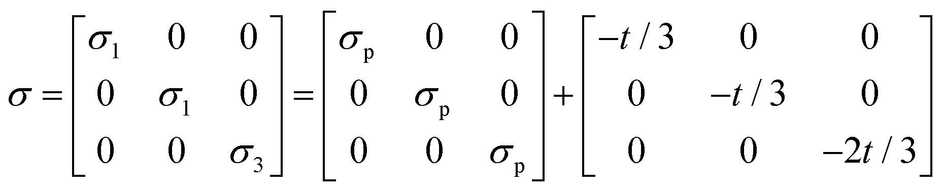 | (1) |
| dm(hkl) = dp(hkl)[1 + (1 − 3cos2φ)Q(hkl)] | (2) |
| t(hkl) = 6G(hkl)Q(hkl) | (3) |
Incompressibility can be determined using the third-order Birch–Murnaghan equation-of-state (EOS)46 as following:
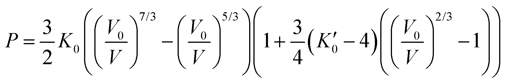 | (4) |
 is the derivative of K0 with respect to P.Eqn (4) can be simplified to second-order by fixing
  . The Birch–Murnaghan equation-of-state can also be rewritten in terms of normalized pressure (F) and Eulerian strain (f),47 as shown in the following:
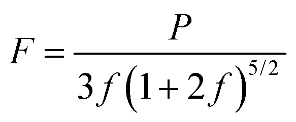 | (5) |
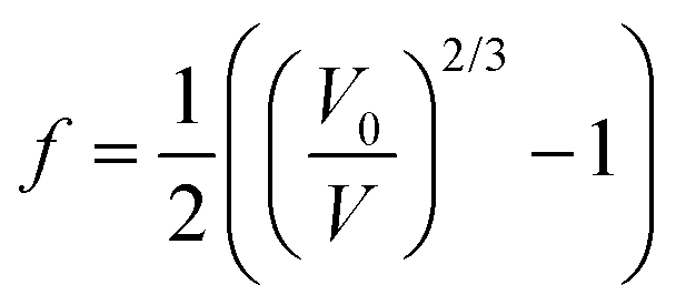 | (6) |
 .
.
Texture analysis was carried out using the software package MAUD.40 The inverse pole figures, representing the variations of intensities along different stress directions, reveal the grain texture and signify the primary slip planes. The texture strength is measured in multiples of the mean random distribution (M.R.D.), with random texture at M.R.D. = 1 and stronger texture at higher M.R.D. values.
3. Results and discussions
3.1. Synthesis of nano-ReB2
In our previous work, we showed that nano-ReB2 could be synthesized by a flux reaction, where the formation of ReB2 from the pure elements could occur at high temperature in a molten salt.31 Here, we worked to tune the particle size through control of nucleation and growth rates with precisely controlled temperature profiles and variation in the precursor-to-salt ratio. In the synthesis of nano-ReB2, excess boron ensures complete formation of borides with the desired stoichiometry. In our previous work, 50 nm particles were prepared with excess NaCl flux, whose liquid phase serves as a diffusion medium as the temperature reaches above its melting point (850 °C).31 The nucleation of nanoparticles occurs above the melting point of NaCl, and the prolonged soaking time ensures the crystal growth. In the current study, larger particles are synthesized with higher temperature and longer soaking time to ensure the full growth of nanoparticles. Smaller particles are synthesized with a higher precursor-to-salt ratio, lower temperature, and shorter soaking time. With a higher precursor-to-salt ratio, nanocrystal nucleation is facilitated, thus initiating the growth of many nanocrystals at once. Faster ramp rates to above the melting temperature of NaCl further facilitates rapid nucleation of nanoparticles. Efficient nucleation is then accompanied by limited growth, which is achieved using short soak times and the lowest temperatures that produce phase pure material to limit grain growth. This combination produces nanocrystals that are significantly smaller than those produced previously.SEM and TEM images (Fig. 1a–f) show the morphology of the 60 nm and 20 nm samples. Both samples appear as large, agglomerated particles which contain many smaller crystalline domains. Atomic resolution microscopy reveals the layered structure of ReB2 with alternating layers of rhenium and boron. The agglomerated morphology and large size of the primary particles make it difficult to determine average crystalline domain sizes with microscopy, so the average grain sizes of the nanocrystalline samples were determined using Rietveld refinement of the peak widths of the X-ray diffraction patterns. In our experiment, a highly crystalline calibration material (CeO2) was used to determine the instrumental broadening. Rietveld analysis for the peak profile from the XRD of the unstressed nano-samples shows crystallite sizes of ∼20 nm, ∼50 nm and ∼60 nm. Overlaying the diffraction patterns of the nano-samples, the peak widths of the diffraction pattern from the 20 nm particles is much wider, and the 50 nm particles have very similar peak width to 60 nm particles, which is consistent with the particle size estimation from Rietveld refinement (Fig. 1g).
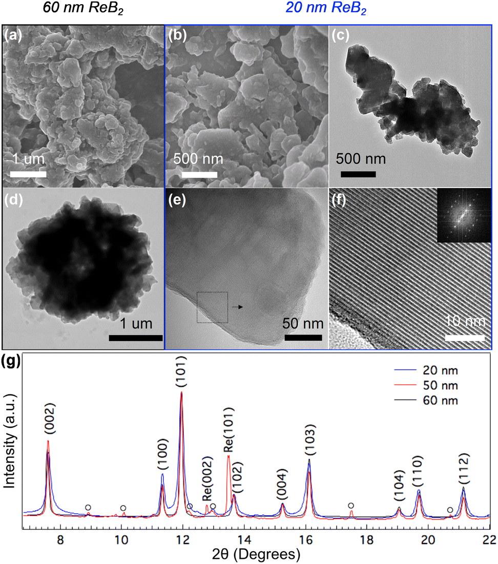 | ||
| Fig. 1 Structural characterization of nano-ReB2. (a) and (b) Scanning electron micrographs of 60 nm and 20 nm ReB2, respectively. (c) and (d) Low magnification transmission electron micrographs of 60 nm and 20 nm ReB2, respectively, showing the grain microstructure within the large primary particles. (e) High resolution transmission electron micrograph of 20 nm ReB2 showing a single lattice domain through a small particle. (f) Atomic resolution image of the selected area in (e) showing the crystal structure of ReB2, with alternating planes of Re (bright) and B (dark). Inset: Fourier transform of the image in (f). (g) 1-D diffraction patterns for 20 nm-, 50 nm-, and 60 nm-ReB2 at ambient pressure. Impurity peaks in the 50 nm-ReB2 are labelled with open circles. | ||
Two-point probe resitivity measurements on nanocrystalline ReB2 shows an ambient temperature resistivity of 1.25 × 10⁻³ Ω cm. This increase in resistivity compared to bulk ReB2 (ρ = 3.5 × 10⁻⁶ Ω cm) is likely caused by the dramatic increase in grain boundaries in the nanocrystalline samples and the fact that the powders were compressed under a very modest load, both of which have been shown to increase resistivity in polycrystalline samples. Despite this, resistivity as a function of temperature shows an increase in resistivity as the temperature rises, indicating that the nanocrystalline samples are still metallic, like their bulk counterparts (Fig. S1, ESI†).
Thermogravimetric analysis (TGA) under dry air shows a small decrease in mass just before 100 °C, followed by an increase at around 400 °C and then a more rapid loss of mass at around 675 °C (Fig S2a, ESI†). The decrease at around 675 °C matches what is seen in bulk ReB2 powder and is attributed to the formation of volatile ReO3 (Fig S2b, ESI†).7 Both the decrease in mass just before 100 °C and the increase in mass starting at 400 °C differ from the bulk, but these can both be attributed to the increased presence of amorphous boron, which is one of the precursors used in the salt flux synthesis. The boron takes in some water when left in air, which is volatilized at around 100 °C, and boron is known to start oxidizing into B2O3 at around 400 °C.48 The data thus indicate that the nanocrystalline ReB2 itself has a very similar thermal stability to bulk ReB2 powders.
3.2. High-pressure radial diffraction
Given that the salt-flux synthesis technique described above only produces small quantities (∼100 mg) of nanocrystalline powder, creating a sintered compact with which direct tensile/shear strength and Vickers hardness measurements can be done is not possible. Instead, we utilize in situ high-pressure X-ray diffraction, which is an experiment uniquely suited to measure the mechanical properties of these nanocrystalline powders. As detailed in the methodology section, extremely small amounts of powder can be loaded into the diamond anvil cell and compressed uniaxially without any pressure medium. These nonhydrostatic conditions create differential compressive stresses within the material that, when combined with lattice strain theories,41,44,49 provide insight into the strength, deformation mechanisms, and elasticity of the materials.50In situ high-pressure XRD experiments were conducted under non-hydrostatic compression up to 50 GPa for 20 nm, 50 nm, and 60 nm-ReB2. The “cake” patterns recorded at the lowest and highest pressures and the integrated 1-dimensional diffraction patterns for the 20 and 60 nm materials are shown in Fig. 2. At low pressure, the diffraction lines are almost straight due to the hydrostatic stress state, while at high pressure, the diffraction lines deviate to higher 2θ values (smaller d-spacings) in the high stress direction (ϕ = 0°) and to lower 2θ values (higher d-spacings) in the low stress direction (ϕ = 90°).33 The sinusoidal variation of each diffraction line indicates the lattice-supported strain. The peak broadening in the high-pressure 1-D integrations is thus due to strain inhomogeneity.
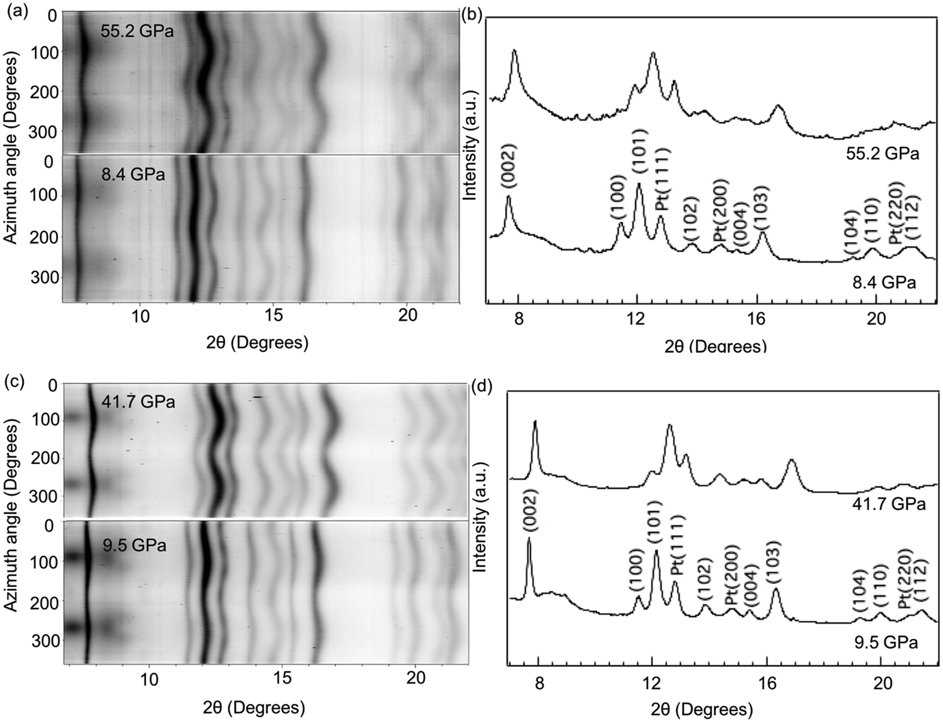 | ||
| Fig. 2 Representative synchrotron cake patterns and integrated 1-D X-ray diffraction patterns for (a) and (b) 20 nm-ReB2 and (c,d) 60 nm-ReB2. The indexing for the relevant peaks is included on the image. | ||
Quasi-hydrostatic high-pressure diffraction patterns can also be obtained at the magic angle ϕ = 54.7°, and all peaks in these patterns can be indexed to the ReB2 crystal structure throughout the measured pressure range. Moreover, the crystal structure is found to be nearly identical before and after compression and decompression, as shown in Fig. S3 (ESI†). This magic angle data can be used to track the change in lattice spacing upon compression (Fig. S4, ESI†). As expected, all peaks shift to higher 2θ values with increasing pressures, but the shift is not identical for different sizes of nanocrystals. We note that as shown in Fig. 2, the diffraction patterns are very smooth, indicating high grain number statistics due to fine particle size. Therefore, Rietveld refinement can be conducted on the high-pressure data, where an entire diffraction pattern can be fit to produce a calculated pattern in an iterative fashion to produce more accurate lattice constants, which are shown as a function of pressure in Fig. 3 and tabulated in Table S1 (ESI†). An example of refined data is shown in Fig. S5 (ESI†). The pressure for each compression step was determined from the equation-of-state of a Pt standard, using its d-spacing at ϕ = 54.7°.
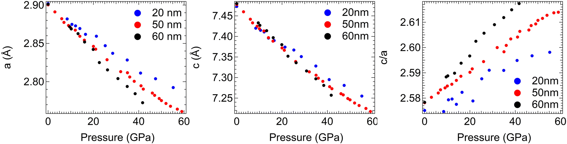 | ||
| Fig. 3 Lattice constants and c/a ratio for 20 nm-, 50 nm- and 60 nm- ReB2 as a function of pressure calculated using Rietveld refinement. | ||
The d-spacings show a continuous, linear decrease without abrupt changes upon compression, suggesting no phase transition occurs and the hexagonal structure is maintained as pressure increases. The lattice constants and their ratio (Fig. 3) show a relatively linear decrease for all three nanocrystalline sizes. The c lattice parameter, which is normal to the boron and metal layers, compresses at a slower rate than the a lattice parameter, resulting in a nonuniform deformation of the unit cell. This can be seen in the positive slope when the c/a ratio is plotted as a function of pressure. The magnitude of this difference appears to be related to the crystalline grain size as well, with the 20 nm-ReB2 having the smallest c/a vs. pressure slope while the 60 nm-ReB2 has the steepest slope. This indicates that smaller sized grains are preferentially more resistant to compression parallel to the boron and metal layers.
With the lattice parameters, bulk modulus can be calculated. Note that the bulk modulus (K0) is sensitive to the choice of pressure derivative  , so that large variations in bulk modulus can result from slight variations in
  .46 As shown in Fig. 4, a fit to the third-order equation-of-state in terms of normalized pressure and Eulerian strain (red line) yields a bulk modulus of 355 ± 9 GPa
  and 393 ± 14 GPa
  for 60 nm- and 20 nm-ReB2, respectively. The second-order equation-of-state with fixed
  (black line) yields a bulk modulus of 304 ± 8 GPa and 406 ± 7 GPa for 60 nm- and 20 nm-ReB2, respectively, but the quality of the fit for the second-order equation is clearly inferior, particularly for the 20-nm nanocrystals.
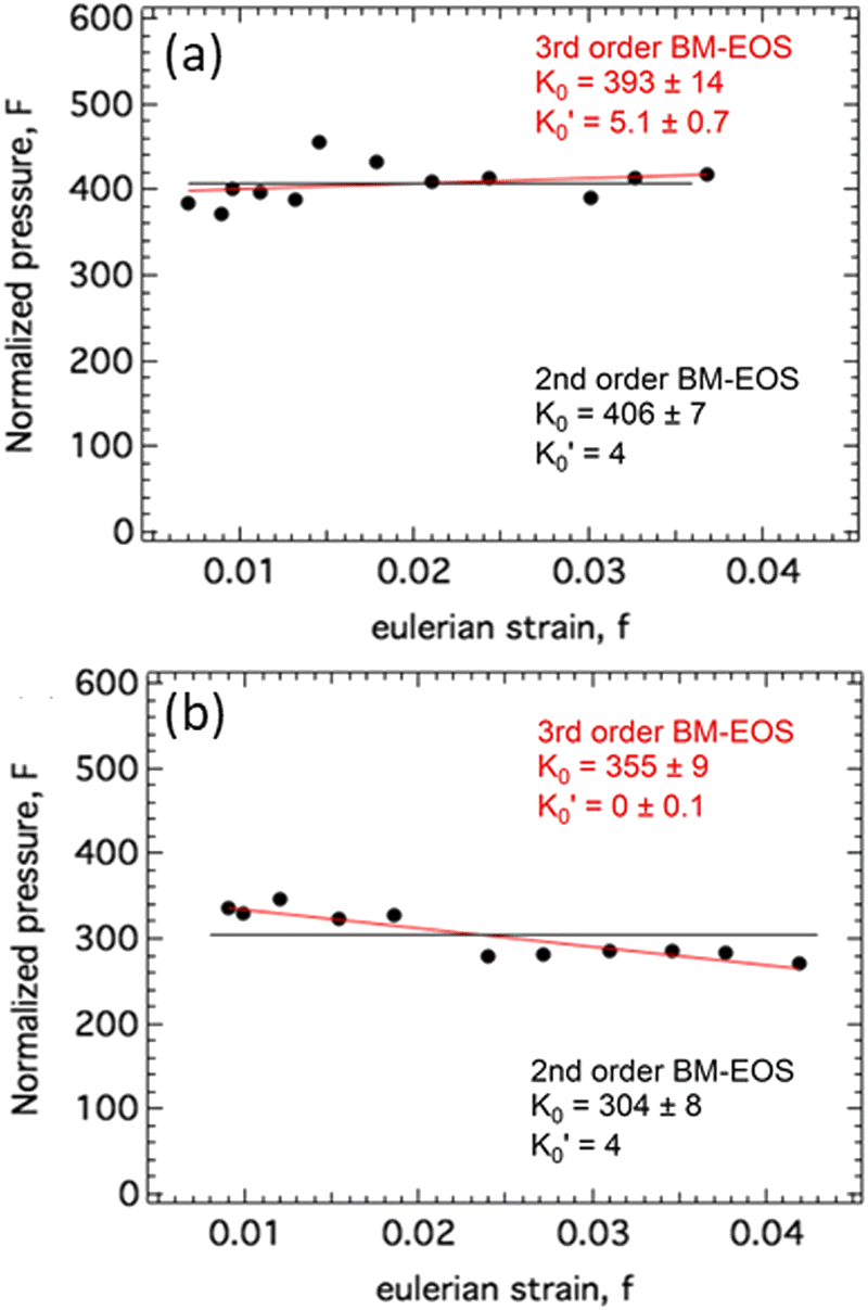 | ||
Fig. 4 Normalized pressure (F) vs. Eularian strain (f) for (a) 20 nm-ReB2 and (b) 60 nm-ReB2. Data points are fit separately to a second-order (black) and a third-order (red) Birch–Murnaghan equation-of-state. The intercept of the solid line yields the ambient pressure bulk modulus (K0). The slope of the line yields the pressure derivative  . . | ||
As shown in Fig. 5, the hydrostatic compression curves, fit to the third-order equation-of-state, shows higher incompressibility in 20 nm-ReB2, compared to 50 or 60-nm materials. The unit cell volume of the smaller particle changes less upon compression and the trend in compressibility is monotonic with size. Similar trends were observed in titania nanoparticles, where it was found that bulk modulus increases with decreasing particle size in the tens of nanometer-scale.51 In that system, it was hypothesized that as the particle size decreases, dislocation pileups become more prevalent due to increasing interaction of the dislocations with interfaces, thus shielding intervening regions from the external pressure.
 | ||
| Fig. 5 Hydrostatic compression curves of 20 nm-, 50 nm- and 60 nm-ReB2 obtained at the magic angle (ϕ = 54.7°). The solid line is fit to the third-order Birch–Murnaghan equation-of-state. | ||
It is true that a high bulk modulus is often observed in hard materials, however, it is not the primary factor in determining materials strength.18,52,53 Bulk modulus, a measure of elastic deformation, reflects a material's resistance to volume change with respect to pressure. Indeed, a number of mechanically soft materials have high bulk moduli.54 Yield strength, on the other hand, defined as the resistance to plastic deformation, is directly related to the hardness of the material.55 In the current study, the plastic deformation mechanism was studied using the evolution of the differential stress (t) as a function of pressure in a lattice specific manner. This is an ideal way to study hardness, as the plateau value of the differential stress corresponds to the yield strength.
As described in the Experimental section, differential stress (t) can be calculated from differential strain (t/G), given the shear modulus (G). It is important to note that shear modulus (G) is a weighted average between the Voigt shear modulus (iso-strain) and the Reuss shear modulus (iso-stress). The differential stress under both conditions was calculated using the elastic stiffness constants.56,57 In Fig. 6, differential stress under iso-strain (tVoigt) conditions are plotted for three different sizes of nano-ReB2 (20 nm, 50 nm,31 60 nm) and bulk ReB2 in a lattice-specific manner. Data are separated both by lattice plane (Fig. 6a) and by sample (Fig. 6b) to compare the data more easily within and between each sample. Differential stress (t) under iso-stress (tReuss) conditions for each sample can be found in the ESI† (Fig. S6, ESI†). Note that the differential stress increases linearly with pressure and then appears to level off. The linear increase is associated with elastic behaviour, and the plateau is interpreted to imply that the lattice plane can no longer sustain additional stress, and presumably indicates the onset of plastic deformation. The plane with the lowest differential stress plateau value supports the least deformation, while planes with higher differential stress plateau values resist more shear and dislocation movement.
 | ||
| Fig. 6 Comparison of the differential stress (t) under iso-strain (tVoigt) conditions as a function of pressure for 20 nm-, 50 nm-, 60 nm- and bulk-ReB2 in the (002), (101) and (110) lattice planes. The data are separated by lattice plane (a) and by sample (b) to more easily compare within and between the different samples. Differential stress (t) under iso-stress (tReuss) conditions for each sample can be found in the ESI† (Fig. S6). | ||
Bulk ReB2 supports much lower differential stress compared to the nano-samples in all three lattice planes studied, suggesting that an enhanced resistance to shear is likely due to the dislocation-grain boundary interaction in the boundary-rich nano samples. In addition, the plateau in bulk ReB2 appears much earlier and is flatter when compared to the nanocrystalline samples, especially in the basal (002) plane. The earlier plateau is indicative of a comparatively more rapid onset of plastic deformation in the bulk sample with slip primarily occurring between the metal–boron layers. In addition, the flatter plateau indicates complete transition from elastic to plastic deformation upon reaching the yield strength. This is in contrast to the nanocrystalline samples which appear to continue some degree of elastic deformation after the onset of plastic deformation, allowing the material to withstand much higher maximum allowed differential stress.
Comparing the differential stress among the nano-ReB2 samples, we found that 20 nm-ReB2 has the highest plateaued value, and the 50 nm-ReB2 has very similar trends in differential stress to the 60 nm-ReB2. This suggests that as the particle size gets significantly smaller, the grain boundary concentration increases, leading to a higher energy barrier for lattice dislocations to propagate through grain boundaries. This phenomenon is known as the Hall–Petch effect, and it states that the strength is inversely proportional to the grain size.58,59 As the grain size decreases, the nucleation of dislocations becomes more energetically unfavorable, leading to material hardening. Interestingly, the 20 nm sample shows a dramatic jump in the differential stress of the (110) plane at around 40 GPa. This appears to be at around the pressure that the basal (002) plane fully plateaus. This is likely indicative of strain hardening behavior as the prismatic (110) planes lock slip, which is accommodated by the movement of the (002) and (101) planes.
The size dependent effects are not the same for all lattice planes. The basal plane of the hexagonal close packed crystal structure, (002), has the lowest plateaued differential stress, implying it is very likely to be the major slip plane. This plane shows the largest size-dependent increase in differential stress, a fact that should translate to large changes in measured hardness in a nanocrystal compact. The (101) and (110) planes, which both cut through the boron and metal layers, support higher plateau values of differential stress. The (101) plane shows very similar differential stress data for all three nanocrystal sizes, though the 20-nm sample appears to be slightly higher.
3.3. Texture analysis
Further information about slip systems in these nanocrystal samples comes from texture analysis, where a direct map of accessible slip systems is derived from the peak intensity variation with stress directions in the radial diffraction geometry. When shear stress is applied to polycrystals in the DAC, individual grains tend to deform preferentially on slip planes, inducing grain rotation to collapse at the lattice-preferred orientation. Such orientation distributions are represented by inverse pole figures (IPF), as shown in Fig. 7 and in other literature.31 In the inverse pole figure, the color scheme indicates the probability of finding the poles to the lattice planes in the compression direction, with a random distribution corresponding to mean random distribution (m.r.d.) = 1, and stronger preferred orientation at higher m.r.d. values. | ||
| Fig. 7 Inverse pole figures for (a) 20 nm- and (b) 60 nm-ReB2 as a function of pressure. For both samples, the (000l) direction is found to be the primary slip system. | ||
In Fig. 7, the IPFs show the evolution of texture for both 20 nm- and 60 nm-ReB2 as a function of pressure. The texture (contrast in m.r.d. intensities) gets stronger as the pressure increases. The trends for the 60 nm ReB2 are very similar to those observed previously for 50 nm ReB2, with the m.r.d. intensity concentrated at the (0001) corner at high pressure. This indicates that the (0001) lattice planes are preferentially orientated perpendicular to the high-stress direction, and thus that (0001)/(001) slips more easily. This confirms that (000l) is indeed the slip plane, in good agreement with the differential strain analysis discussed above and with the theoretical slip system of (001)[1![[1 with combining macron]](https://www.rsc.org/images/entities/char_0031_0304.gif) 0] for ReB2.60 Interestingly, 20 nm-ReB2 does not show the same monotonic increase in texture. It exhibits decreasing texture from 35 GPa to 41 GPa, followed by increasing texture to 55 GPa. This finding is in good agreement with the strain hardening observed in Fig. 6. A plateau in the differential stress indicates slipping of a lattice plane, whereas an increasing differential stress value indicates resistance to the slip. The significant increase in differential stress for the (110) lattice plane of 20 nm-ReB2 from 35 GPa to 41 GPa suggests a greater ability of smaller particles to resist slipping at the basal plane, which results in a weaker texture. At the highest pressure (55 GPa), nanoparticles eventually fail to resist slip, and therefore, stronger texture was observed. As shown in the IPF at 55 GPa, higher m.r.d. intensities are again more concentrated at the (0001) corner, as expected for basal plane slip.
0] for ReB2.60 Interestingly, 20 nm-ReB2 does not show the same monotonic increase in texture. It exhibits decreasing texture from 35 GPa to 41 GPa, followed by increasing texture to 55 GPa. This finding is in good agreement with the strain hardening observed in Fig. 6. A plateau in the differential stress indicates slipping of a lattice plane, whereas an increasing differential stress value indicates resistance to the slip. The significant increase in differential stress for the (110) lattice plane of 20 nm-ReB2 from 35 GPa to 41 GPa suggests a greater ability of smaller particles to resist slipping at the basal plane, which results in a weaker texture. At the highest pressure (55 GPa), nanoparticles eventually fail to resist slip, and therefore, stronger texture was observed. As shown in the IPF at 55 GPa, higher m.r.d. intensities are again more concentrated at the (0001) corner, as expected for basal plane slip.
Comparing the data for the 20 nm- and 60 nm- ReB2 at the highest pressure collected for the 60 nm- sample (42 GPa) shows significant differences. At a similar pressure (41 GPa), 20 nm-ReB2 has weaker texture, especially at the (0001) corner, implying that slip systems are suppressed in the smaller crystallites, which results in higher differential stress. Similar size dependence of texture has been observed in a number of metal nanocrystal systems.30,61,62 In the nickel nanocrystals, for example, nano-Ni with smaller grain sizes shows weaker texture, indicating that dislocation becomes less active with decreasing grain size.30 Since ReB2 is much tougher than soft materials like Ni, the dislocation creep on preferred slip systems is less significant, and therefore the texture is much weaker, with an m.r.d. value of only ∼1.3 at the highest pressure in our experiment, but the same trend of size-dependent texture follows. The texture results, together with strain analysis, suggest that grain boundary effects are key to impeding dislocation, thus influencing the plastic deformation mechanism in the nanosized superhard metal borides.
4. Conclusions
In this paper, we used a molten salt flux growth method to produce nanoscale ReB2 ranging in size from 20 nm to 60 nm through control over nanocrystal nucleation kinetics. In situ high-pressure radial XRD was performed under nonhydrostatic compression up to ∼50 GPa. The equation-of-state for nano-ReB2 samples were calculated from d-spacings under hydrostatic condition (ϕ = 54.7°) and the bulk moduli were obtained. The results indicate that the bulk modulus was significantly increased in the smaller crystallites. Lattice-specific differential strain analysis was performed on 20, 50, and 60 nm-ReB2 and the results were compared with bulk ReB2. The yield strength was found to be inversely proportional to grain size, in good agreement with the Hall–Petch effect. The basal planes of the samples support the least differential stress confirming that (00l) is the slip plane controlling deformation in all sizes of ReB2. Texture analysis confirmed the slip system and showed a size dependence to the development of texture in nano-ReB2; weaker texture was observed in the smaller nanocrystals. This fact, coupled with the strong correlation between yield strength and texture, indicates that grain boundaries in these superhard materials can dramatically reduce dislocation-induced plastic deformation.Although this is a fundamental study of nanocrystal powders, spark plasma sintering (SPS) could be used in the future to produce a densified nanostructured ceramic from these nanocrystals, thereby allowing for more standard indentation hardness measurements and comparison with other superhard materials. In the meantime, these results have exciting implications for the enhanced hardness of nanostructured metal boride ceramics that may be produced from these precursors.
Conflicts of interest
There are no conflicts to declare.Acknowledgements
The authors thank M. Kunz, B. Kalkan and K. Armstrong for technical support at the Lawrence Berkeley National Laboratory (LBNL) beamline 12.2.2. This work was financially supported by the National Science Foundation Division of Materials Research under grants DMR-2004616 and DMR-2312942 (R. B. K. and S. H. T.). D. D. R. acknowledges support from a National Science Foundation Graduate Research Fellowship under Grant No. DGE-2034835. Radial diffraction experiments were performed at the Advanced Light Source at Lawrence Berkely National Laboratory at Beamline 12.2.2. Beamline 12.2.2 at the Advanced Light Source is a DOE Office of Science User Facility supported under contract no. DE-AC02-05CH11231. This research was partially supported by COMPRES, the Consortium for Materials Properties Research in Earth Sciences under NSF Cooperative Agreement EAR 1606856.References
- R. Komanduri and M. C. Shaw, Nature, 1975, 255, 211–213 CrossRef CAS.
- T. Taniguchi, M. Akaishi and S. Yamaoka, J. Am. Ceram. Soc., 1996, 79, 547–549 CrossRef CAS.
- J. E. Westraadt, I. Sigalas and J. H. Neethling, Int. J. Refract. Met. Hard Mater., 2015, 48, 286–292 CrossRef CAS.
- J. B. Levine, S. H. Tolbert and R. B. Kaner, Adv. Funct. Mater., 2009, 19, 3519–3533 CrossRef CAS.
- H.-Y. Chung, M. B. Weinberger, J. B. Levine, A. Kavner, J.-M. Yang, S. H. Tolbert and R. B. Kaner, Science, 2007, 316, 436–439 CrossRef CAS PubMed.
- R. B. Kaner, J. J. Gilman and S. H. Tolbert, Science, 2005, 308, 1268–1269 CrossRef CAS.
- J. B. Levine, S. L. Nguyen, H. I. Rasool, J. A. Wright, S. E. Brown and R. B. Kaner, J. Am. Chem. Soc., 2008, 130, 16953–16958 CrossRef CAS PubMed.
- M. Xie, R. Mohammadi, Z. Mao, M. M. Armentrout, A. Kavner, R. B. Kaner and S. H. Tolbert, Phys. Rev. B: Condens. Matter Mater. Phys., 2012, 85, 064118 CrossRef.
- J. Qin, D. He, J. Wang, L. Fang, L. Lei, Y. Li, J. Hu, Z. Kou and Y. Bi, Adv. Mater., 2008, 20, 4780–4783 CrossRef CAS.
- H.-Y. Chung, M. B. Weinberger, J.-M. Yang, S. H. Tolbert and R. B. Kaner, Appl. Phys. Lett., 2008, 92, 261904 CrossRef.
- S. N. Tkachev, J. B. Levine, A. Kisliuk, A. P. Sokolov, S. Guo, J. T. Eng and R. B. Kaner, Adv. Mater., 2009, 21, 4284–4286 CrossRef CAS.
- H.-Y. Chung, M. B. Weinberger, J. B. Levine, R. W. Cumberland, A. Kavner, J.-M. Yang, S. H. Tolbert and R. B. Kaner, Science, 2007, 318, 1550 CrossRef.
- A. Latini, J. V. Rau, D. Ferro, R. Teghil, V. R. Albertini and S. M. Barinov, Chem. Mater., 2008, 20, 4507–4511 CrossRef CAS.
- J. Chrzanowska, J. Hoffman, P. Denis, M. Giżyński and T. Mościcki, Surf. Coat. Technol., 2015, 277, 15–22 CrossRef CAS.
- P. Lazar, X.-Q. Chen and R. Podloucky, Phys. Rev. B: Condens. Matter Mater. Phys., 2009, 80, 012103 CrossRef.
- W. Zhou, H. Wu and T. Yildirim, Phys. Rev. B: Condens. Matter Mater. Phys., 2007, 76, 184113 CrossRef.
- M.-M. Zhong, X.-Y. Kuang, Z.-H. Wang, P. Shao, L.-P. Ding and X.-F. Huang, J. Alloys Compd., 2013, 581, 206–212 CrossRef CAS.
- M. T. Yeung, R. Mohammadi and R. B. Kaner, Annu. Rev. Mater. Res., 2016, 46, 465–485 CrossRef CAS.
- M. Xie, R. Mohammadi, C. L. Turner, R. B. Kaner, A. Kavner and S. H. Tolbert, Appl. Phys. Lett., 2015, 107, 041903 CrossRef.
- L. E. Pangilinan, C. L. Turner, G. Akopov, M. Anderson, R. Mohammadi and R. B. Kaner, Inorg. Chem., 2018, 57, 15305–15313 CrossRef CAS PubMed.
- G. Akopov, I. Roh, Z. C. Sobell, M. T. Yeung and R. B. Kaner, Dalton Trans., 2018, 47, 6683–6691 RSC.
- A. Mansouri Tehrani, A. O. Oliynyk, Z. Rizvi, S. Lotfi, M. Parry, T. D. Sparks and J. Brgoch, Chem. Mater., 2019, 31, 7696–7703 CrossRef CAS.
- A. T. Lech, C. L. Turner, J. Lei, R. Mohammadi, S. H. Tolbert and R. B. Kaner, J. Am. Chem. Soc., 2016, 138, 14398–14408 CrossRef CAS.
- Y. Li, A. J. Bushby and D. J. Dunstan, Proc. R. Soc. A, 2016, 472, 20150890 CrossRef CAS PubMed.
- Q. Huang, D. Yu, B. Xu, W. Hu, Y. Ma, Y. Wang, Z. Zhao, B. Wen, J. He, Z. Liu and Y. Tian, Nature, 2014, 510, 250–253 CrossRef CAS.
- H. Sumiya and T. Irifune, J. Mater. Res., 2007, 22, 2345–2351 CrossRef CAS.
- C. Huang, B. Yang, X. Peng and S. Chen, ACS Appl. Mater. Interfaces, 2020, 12, 50161–50175 CrossRef CAS PubMed.
- B. Zhao, S. Zhang, S. Duan, J. Song, X. Li, B. Yang, X. Chen, C. Wang, W. Yi, Z. Wang and X. Liu, Nanoscale Adv., 2020, 2, 691–698 RSC.
- B. Chen, Texture of Nanocrystalline Nickel DOI:10.1126/science.1228211, (accessed 24 April 2022).
- X. Zhou, Z. Feng, L. Zhu, J. Xu, L. Miyagi, H. Dong, H. Sheng, Y. Wang, Q. Li, Y. Ma, H. Zhang, J. Yan, N. Tamura, M. Kunz, K. Lutker, T. Huang, D. A. Hughes, X. Huang and B. Chen, Nature, 2020, 579, 67–72 CrossRef CAS PubMed.
- J. Lei, S. Hu, C. L. Turner, K. Zeng, M. T. Yeung, J. Yan, R. B. Kaner and S. H. Tolbert, ACS Nano, 2019, 13, 10036–10048 CrossRef CAS.
- A. L. Ruoff, J. Appl. Phys., 1975, 46, 1389–1392 CrossRef CAS.
- A. K. Singh, J. Appl. Phys., 2009, 106, 043514 CrossRef.
- R. J. Hemley, H. Mao, G. Shen, J. Badro, P. Gillet, M. Hanfland and D. Häusermann, Science, 1997, 276, 1242–1245 CrossRef CAS.
- S. Merkel, N. Miyajima, D. Antonangeli, G. Fiquet and T. Yagi, J. Appl. Phys., 2006, 100, 023510 CrossRef.
- S. M. Dorfman, S. R. Shieh and T. S. Duffy, J. Appl. Phys., 2015, 117, 065901 CrossRef.
- S. Merkel and T. Yagi, Rev. Sci. Instrum., 2005, 76, 046109 CrossRef.
- A. P. Hammersley, S. O. Svensson, M. Hanfland, A. N. Fitch and D. Hausermann, High Press. Res., 1996, 14, 235–248 CrossRef.
- H. M. Rietveld, J. Appl. Crystallogr., 1969, 2, 65–71 CrossRef CAS.
- L. Lutterotti, S. Matthies, H.-R. Wenk, A. S. Schultz and J. W. Richardson, J. Appl. Phys., 1997, 81, 594–600 CrossRef CAS.
- A. K. Singh, J. Appl. Phys., 1993, 73, 4278–4286 CrossRef.
- W. Voigt, Lehrbuch der Kristallphysik (mit Ausschluss der Kristalloptik), 1966 Search PubMed.
- A. Reuss, J. Appl. Math. Mech./Z. Angew. Math. Mech., 1929, 9, 49–58 CrossRef CAS.
- A. K. Singh, C. Balasingh, H. Mao, R. J. Hemley and J. Shu, J. Appl. Phys., 1998, 83, 7567–7575 CrossRef CAS.
- R. F. S. Hearmon, Adv. Phys., 1956, 5, 323–382 CrossRef.
- F. Birch, J. Geophys. Res.: Solid Earth, 1978, 83, 1257–1268 CrossRef CAS.
- C. Meade and R. Jeanloz, Geophys. Res. Lett., 1990, 17, 1157–1160 CrossRef.
- P. K. Ojha, R. Maji and S. Karmakar, Combust. Flame, 2018, 188, 412–427 CrossRef CAS.
- A. K. Singh and C. Balasingh, J. Appl. Phys., 1994, 75, 4956–4962 CrossRef CAS.
- J. Liu, Chin. Phys. B, 2016, 25, 076106 CrossRef.
- B. Chen, H. Zhang, K. A. Dunphy-Guzman, D. Spagnoli, M. B. Kruger, D. V. S. Muthu, M. Kunz, S. Fakra, J. Z. Hu, Q. Z. Guo and J. F. Banfield, Phys. Rev. B: Condens. Matter Mater. Phys., 2009, 79, 125406 CrossRef.
- C.-M. Sung and M. Sung, Mater. Chem. Phys., 1996, 43, 1–18 CrossRef CAS.
- T. Kenichi, Phys. Rev. B: Condens. Matter Mater. Phys., 2004, 70, 012101 CrossRef.
- L. Dubrovinsky, N. Dubrovinskaia, E. Bykova, M. Bykov, V. Prakapenka, C. Prescher, K. Glazyrin, H.-P. Liermann, M. Hanfland, M. Ekholm, Q. Feng, L. V. Pourovskii, M. I. Katsnelson, J. M. Wills and I. A. Abrikosov, Nature, 2015, 525, 226–229 CrossRef CAS PubMed.
- D. He, S. R. Shieh and T. S. Duffy, Phys. Rev. B: Condens. Matter Mater. Phys., 2004, 70, 184121 CrossRef.
- M.-M. Zhong, X.-Y. Kuang, Z.-H. Wang, P. Shao, L.-P. Ding and X.-F. Huang, J. Phys. Chem. C, 2013, 117, 10643–10652 CrossRef CAS.
- J. B. Levine, J. B. Betts, J. D. Garrett, S. Q. Guo, J. T. Eng, A. Migliori and R. B. Kaner, Acta Mater., 2010, 58, 1530–1535 CrossRef CAS.
- E. O. Hall, Proc. Phys. Soc., London, Sect. B, 1951, 64, 747–753 CrossRef.
- N. J. Petch, J. Iron Steel Inst., 1953, 174, 25–28 CAS.
- C. Zang, H. Sun, J. S. Tse and C. Chen, Phys. Rev. B: Condens. Matter Mater. Phys., 2012, 86, 014108 CrossRef.
- J. Schiøtz, F. D. Di Tolla and K. W. Jacobsen, Nature, 1998, 391, 561–563 CrossRef.
- B. Chen, K. Lutker, J. Lei, J. Yan, S. Yang and H. Mao, Proc. Natl. Acad. Sci. U. S. A., 2014, 111, 3350–3353 CrossRef CAS PubMed.
Footnotes |
| † Electronic supplementary information (ESI) available. See DOI: https://doi.org/10.1039/d3nh00489a |
| ‡ These authors contributed equally to this work. |
| This journal is © The Royal Society of Chemistry 2024 |