
An ultra-sensitive colloidal quantum dot infrared photodiode exceeding 100![[thin space (1/6-em)]](https://www.rsc.org/images/entities/h2_char_2009.gif) 000% external quantum efficiency via photomultiplication†
000% external quantum efficiency via photomultiplication†
Byung Ku
Jung‡
 a,
Taesung
Park‡
a,
Young Kyun
Choi
a,
Yong Min
Lee
a,
Tae Hyuk
Kim
b,
Bogyeom
Seo
c,
Seongkeun
Oh
a,
Jae Won
Shim
b,
Yu-hwa
Lo
c,
Tse Nga
Ng
c and
Soong Ju
Oh
*a
a,
Taesung
Park‡
a,
Young Kyun
Choi
a,
Yong Min
Lee
a,
Tae Hyuk
Kim
b,
Bogyeom
Seo
c,
Seongkeun
Oh
a,
Jae Won
Shim
b,
Yu-hwa
Lo
c,
Tse Nga
Ng
c and
Soong Ju
Oh
*a
aDepartment of Materials Science and Engineering, Korea University, 145, Anam-ro, Seongbuk-gu, Seoul 02841, Republic of Korea. E-mail: sjoh1982@korea.ac.kr
bSchool of Electrical Engineering, Korea University, Seoul 02841, Republic of Korea
cDepartment of Electrical and Computer Engineering, University of California San Diego, La Jolla, California 92093-0407, USA
First published on 15th January 2024
Abstract
In this study, we present ultrasensitive infrared photodiodes based on PbS colloidal quantum dots (CQDs) using a double photomultiplication strategy that utilizes the accumulation of both electron and hole carriers. While electron accumulation was induced by ZnO trap states that were created by treatment in a humid atmosphere, hole accumulation was achieved using a long-chain ligand that increased the barrier to hole collection. Interestingly, we obtained the highest responsivity in photo-multiplicative devices with the long ligands, which contradicts the conventional belief that shorter ligands are more effective for optoelectronic devices. Using these two charge accumulation effects, we achieved an ultrasensitive detector with a responsivity above 7.84 × 10² A W−1 and an external quantum efficiency above 105% in the infrared region. We believe that the photomultiplication effect has great potential for surveillance systems, bioimaging, remote sensing, and quantum communication.
New conceptsPbS colloidal quantum dots have been widely considered attractive IR absorbing materials due to their programmable absorption range from visible to short wavelength IR, high intrinsic absorption coefficient (>104 cm−1), and high electron and hole mobility (>10−1 cm V−1 s−1). While PbS CQD thin film IR photodiodes (PDs) exhibit high performance, such as external quantum efficiency of 80% comparable to commercial infrared photodetectors, further improvement is required for potential applications in quantum communications, bioimaging, lidar, etc. In this work, we present a highly efficient PbS CQD-based multiplication-type photodiode exceeding 100![[thin space (1/6-em)]](https://www.rsc.org/images/entities/char_2009.gif) 000% using the double charge accumulation strategy. The charge accumulation strategy was achieved by the utilization of long ligand encapsulated NC thin films, inducing band-bending induced tunneling-based photomultiplication. Combinatorial analysis indicates a direct correlation between accumulated charge density and the photomultiplication process. We believe that our findings will not only serve as a source of inspiration for improving the EQEs of photomultiplication-type photodiodes, but also significantly contribute to next generation quantum optics and optoelectronics. 000% using the double charge accumulation strategy. The charge accumulation strategy was achieved by the utilization of long ligand encapsulated NC thin films, inducing band-bending induced tunneling-based photomultiplication. Combinatorial analysis indicates a direct correlation between accumulated charge density and the photomultiplication process. We believe that our findings will not only serve as a source of inspiration for improving the EQEs of photomultiplication-type photodiodes, but also significantly contribute to next generation quantum optics and optoelectronics.
|
Introduction
Infrared (IR) photodetectors are in great demand owing to their applications in light detection and ranging (LiDAR) sensors, optical communication, driverless vehicles, and security systems.1–4 In particular, photomultiplication-type IR photodiodes (PDs) have been reported to have great advantages in detecting weak light without a photocurrent amplification system, yielding great potential for advanced applications5–9 such as IR-to-visible upconversion, bioimaging, remote sensing, and quantum communication. To date, narrow-bandgap IR-absorbing materials, such as epitaxially grown III–V semiconductors (InGaAs and InSb) or Hg1−xCdxTe, have been used to effectively absorb IR radiation and achieve highly sensitive photomultiplication-type IR PDs.10–12 Unfortunately, these materials require high-temperature or vacuum processing; these processes increase the cost of IR photodetectors and limit their application in industrial and military fields.Colloidal quantum dots (CQDs) are promising next-generation materials for optoelectronic devices because of their low-temperature solution-based processability13–15 coupled with high adsorption and crystalline robustness, which allow them to be directly deposited on silicon readout integrated circuits.16,17 In particular, lead chalcogenide (PbE) (PbS and PbSe) CQDs have been used as IR absorbing materials owing to their widely programmable absorption range from visible to short wavelength IR coupled with their high intrinsic absorption coefficient (>104 cm−1) and high electron and hole mobility (>10−1 cm V−1 s−1).18–25 The physical properties of PbS CQD thin films have been precisely controlled at the material level, and numerous studies have attempted to increase the surface ligand density to eliminate dangling bonds that generate deep mid-gap states and capture photogenerated carriers. The energy level of the PbS CQD thin film has been modified by tailoring its stoichiometry to minimize the energy barrier between the layers that constitute the optoelectronic devices and induce directional carrier diffusion. Various deposition methods such as spin-, blade-, and meniscus-guided coatings have been developed to fabricate densely packed PbS CQD thin films.26–28 As a result of these efforts, PbS CQD-based optoelectronics have reported outstanding performance in various devices, such as phototransistors, photoconductors, and PDs. In particular, PbS CQD-based IR PDs also exhibit high external quantum efficiency (EQE) (>50%) and detectivity (>1012 Jones) in the IR range. Although various PbS CQD-based optoelectronics have been reported, only a few studies have reported photomultiplication-type quantum-dot photodiodes (PM-QPDs),29,30 and further improvement in their responsivity is still needed.
In this work, we present a double photomultiplication strategy that induced the accumulation of both electron and hole carriers and report a sensitive PM-QPD. We designed PM-QPD devices where the charge accumulations occurred at the electron-/hole-transporting layer (ETL/HTL) by electron and hole carriers, respectively. Subsequently, the band bending amplifies photogenerated carriers by accelerating charge injection by tunneling from electrodes above a threshold voltage. Electron accumulation was realized through trap states induced by exposing ZnO thin film (ETL) in a humid atmosphere, resulting in enhancing energy-level bending and tunneling of hole carriers from the bottom electrode. Hole accumulation was initiated by a bottleneck effect originating from the difference in hole mobility between the IR absorbing layer and the oleic acid (OA) passivated PbS thin film (HTL). Although it is commonly believed that shorter ligands are more effective for optoelectronic devices, we intentionally utilized an OA passivated layer (PbS-OA) to efficiently hinder the hole carrier extraction from the HTL to the electrode and to accumulate the holes towards energy-level bending. This design leads to electrons tunneling from the top electrode and enlarges the multiplication effect. Combinational studies of structural, optical, and electrical analyses were conducted to demonstrate the double photomultiplication strategy. The optimized PM-QPD achieves an EQE > 105%, which is the highest EQE among reported PM-QPDs to the best of our knowledge.
Results and discussion
The ∼4 nm size PbS CQDs were synthesized via the hot injection method. For the IR absorbing layer, halide ligand-passivated PbS QD thin films (PbS-halide) were used. For the HTL, ethane-1,2-dithiol (PbS-EDT) and oleic acid-passivated (PbS-OA) PbS QD thin films were prepared, while for the ETL a ZnO thin film was used, as detailed in the Experimental section. Their structural and physical properties were analyzed using transmission electron microscopy, UV-vis, and ultraviolet photoelectron spectroscopy in Fig. S1 (ESI†). In Fig. 1A, a conventional PbS-QPD with an indium tin oxide (ITO)/ZnO/PbS-halide/PbS-EDT/Au structure is shown, and the fabrication processes are described in the Experimental section. In the conventional PbS-QPD structure, photogenerated carriers are extracted without any multiplication effects. In this study, we introduced a double photomultiplication strategy via the ETL and HTL to assist in charge accumulation, as shown in Fig. 1B and C, respectively. First, the density of trap states at the ETL was precisely controlled by the treatment of the ZnO thin films in a humid atmosphere. These trap states capture electron carriers and form a local electrical field that additionally accelerates band bending with an external bias. Above the threshold voltage Vth, hole carriers are injected from the ITO electrode via a tunneling effect from the ITO electrode (Fig. 1B). Second, we intentionally designed a large difference in the hole carrier mobility between the HTL and the PbS halide to accumulate hole carriers by using PbS-OA as the HTL. Considering that the carrier velocity is proportional to the mobility and external bias, more hole carriers accumulate in the HTL when a higher external voltage is applied. Above Vth, the local electrical field triggered electron carrier tunneling from the Au electrode (Fig. 1C).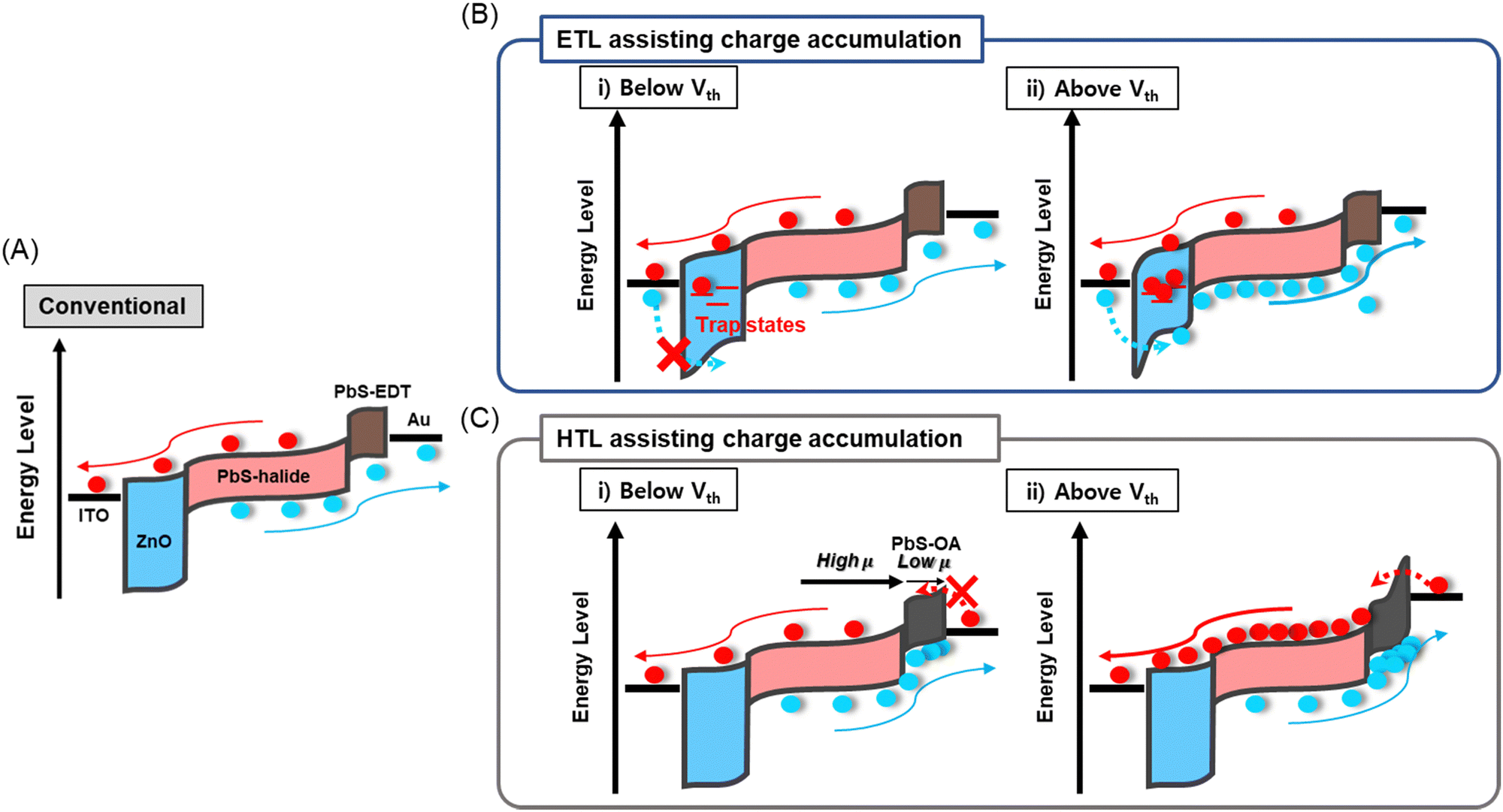 | ||
| Fig. 1 Schematic of carrier dynamics in (A) conventional PbS CQD-based IR PD and (B) ETL and (C) HTL-assisted charge accumulation strategies. | ||
To induce defect states in the ZnO layer that capture electron carriers, we performed humidity treatment on the as-synthesized ZnO thin films. ZnO thin films were deposited by spin coating under dry conditions (ZnO-pristine) (relative humidity <20%), and then, ZnO-pristine was stored in a humid chamber (ZnO-hydrated) (relative humidity >80%) (Fig. 2A). To analyse the effect of the humidity treatment on the optical properties of the ZnO thin films, the FTIR spectra of the ZnO thin films before (ZnO-pristine) and after treatment (ZnO-hydrated) were measured (Fig. 2B). Several peaks were observed at 2800–3000 cm−1 (C–H stretching) and two peaks at 1571 cm−1 and 1417 cm−1 (COO−) stemming from the zinc acetate precursor.31–33 In addition, a broad O–H stretching peak at 3500 cm−1 corresponds to the OH− ligand of the ZnO nanoparticles (NPs). After humidity treatment, while the intensities of the peaks related to acetates decreased, the O–H stretching peak increased, as observed in the FTIR spectrum of ZnO-hydrated.34 These results indicate the disappearance of acetate molecules located on the ZnO NP surface owing to the sintering effect and the attachment of water molecules on the surface of the ZnO NPs. UV-vis and photoluminescence (PL) results (Fig. S2, ESI†) are discussed in Note S1 (ESI†).
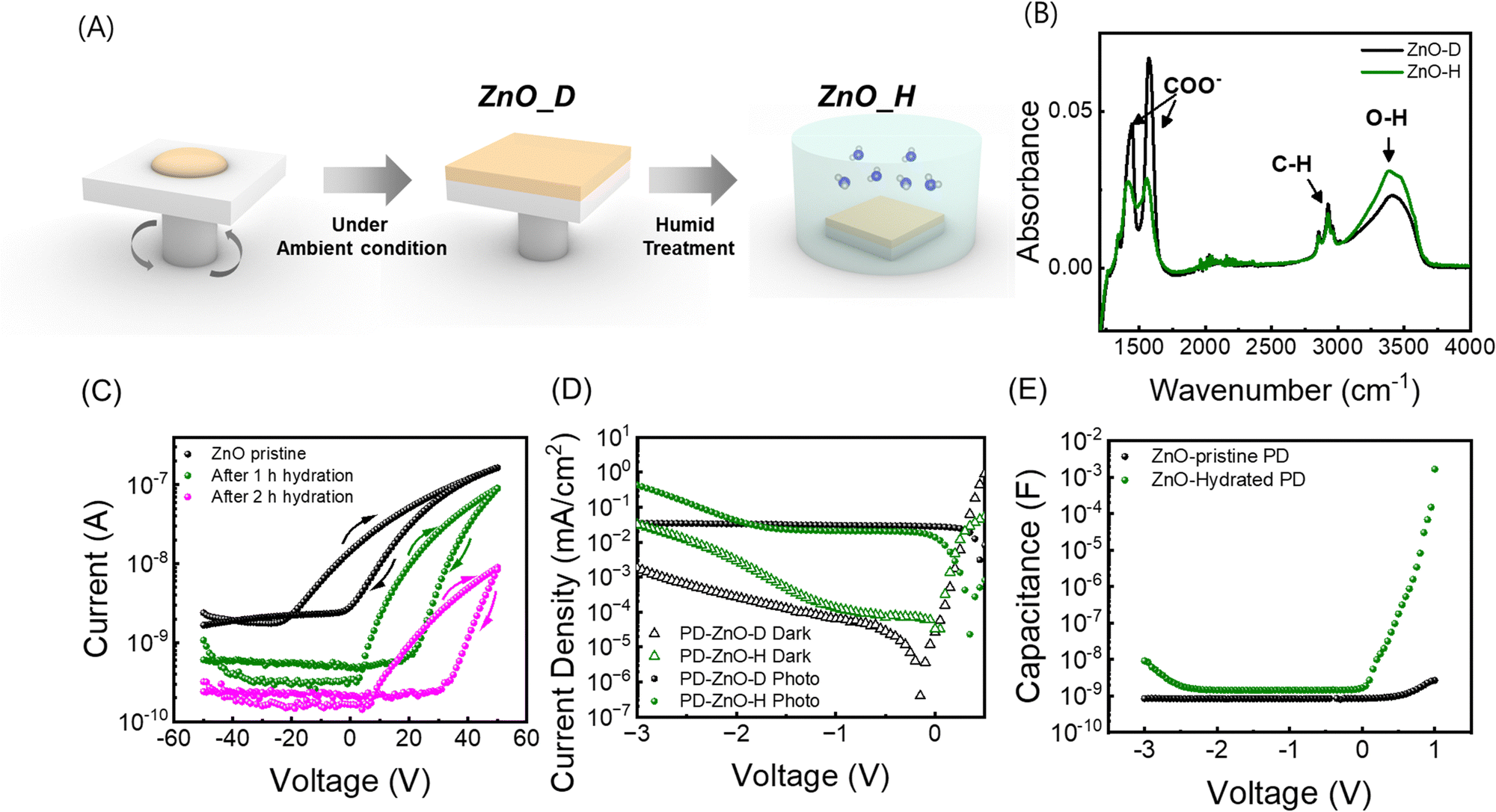 | ||
| Fig. 2 (A) Fabrication process of the ETL without (ZnO-pristine) and with humidity treatment (ZnO-hydrated). (B) Fourier-transform IR spectroscopy (FTIR) spectra of ZnO-pristine and ZnO-hydrated. (C) The source–drain current (IDS) vs. gate voltage (VG) curve of the ZnO thin film-based FET transistor by humidity treatment. (D) Current density–voltage (J–V) of PbS QPDs using ZnO-pristine and ZnO-hydrated measured under the dark state and 980 nm illumination with an intensity of 13 μW cm−2. (E) Capacitance–voltage curves (C–V) of PbS QPDs. | ||
To measure the effect of humidity treatment on the electrical properties of the ZnO thin films, we measured the electron mobility using a field-effect transistor (FET) (Fig. 2C).34 The transfer curve of pristine ZnO exhibited a turn-on voltage at VG = 15.9 V, and the calculated electron mobility was 6.45× 10⁻⁴ cm2 V−1 s−1 in the saturation regime. After 1 h of humidity treatment, the transfer curve revealed a large increase in the turn-on voltage to 36.1 V, a slight decrease of the electron mobility to 4.97 × 10⁻⁴ cm2 V−1 s−1, and a slight increase of the device hysteresis (Fig. S3, ESI†). After 2 h of humidity treatment, the turn-on voltage and the mobility became 42.6 V and 3.67 × 10⁻⁵ cm2 V−1 s−1, respectively. Considering that the turn-on voltage in n-type TFTs positively shifts when the doping level increases, humidity treatment decreases both the charge carrier mobility and density in ZnO thin films. We attributed these results to the formation of defect trap states in ZnO films under humidity treatment.
We fabricated two different PbS QPDs using ZnO-pristine and 1 h of humidity treated ZnO-hydrated as the ETL, denoted as PD with ZnO-pristine and PD with ZnO-hydrated, respectively. It should be noted that long time humidity treatment (>2 h) deteriorates the photodiode performance as it creates too many defects and reduces the mobility (Fig. S3, ESI†). In Fig. 2D, the J–V curves of the two devices are shown in the dark and under illumination. PD with ZnO-pristine exhibited a saturated photocurrent density as the value of the reverse bias increased. In contrast, PD with ZnO-hydrated (1 h) exhibited a saturated photocurrent density at a low reverse bias, but a rapid increase in photocurrent density was observed above the threshold voltage (Vth-J). Vth-J was calculated from the derivative of photocurrent density with respect to the voltage versus voltage graph (dJphoto/dV–V) and found to be −1.8 V. To further investigate the reason for photomultiplication in the devices, C–V curves were measured from −3 V to 1 V. While PD with ZnO-pristine exhibited a constant capacitance independent of the applied reverse bias, PD with ZnO-hydrated initially showed a constant capacitance, but a rapid increase occurred above the threshold voltage, which is similar to its J–V curve (Fig. 2E). The threshold voltage of capacitance (Vth-C) was confirmed from the derivative of the capacitance with respect to the voltage versus voltage graph (dC/dV–V) and found to be −1.9 V (Fig. S4, ESI†). It is important to note that the Vth-C of PD with ZnO-hydrated was similar to Vth-J of PD with ZnO-hydrated, with a slight difference, implying that the origin of photocurrent amplification was closely related to charge accumulation in the device.
To maximize the band-bending-induced tunneling and photomultiplication effects, we designed a device geometry with large hole carrier accumulation at the HTL. For efficient hole carrier accumulation at the HTL, low-mobility HTL materials were chosen to increase the hole mobility difference between the PbS halide and HTL layers. The carrier mobility in QD films is inversely proportional to the ligand length and the number of carbon chains in the ligands. Therefore, instead of the conventional EDT (2 carbon) ligand, we introduce an oleic acid (18 carbon)-passivated PbS CQD thin film as the HTL to maximize the hole mobility difference between the PbS-halide (0 carbon) and HTL. From the transfer curve of the FET device, the hole carrier mobility of PbS-EDT was determined to be 2.57 × 10⁻⁴ cm2 V−1 s−1 in the saturation regime, while that of PbS-OA could not be measured because of its considerably low mobility (Fig. S5, ESI†). To further examine the hole carrier mobilities of PbS-EDT and PbS-OA, the vertical structures with hole-only devices (ITO/PEDOT:PSS/HTL/MoO3/Au) were prepared, and space charge limited measurements (SCLC) were conducted (Fig. 3A). The J–V curve measured from the SCLC was fitted using the Mott–Gurney law.2,35 The hole mobility of each QD film was determined from the SCLC region (slope = 2). The hole mobilities of PbS-EDT and PbS-OA were found to be μh,EDT = 1.6 × 10⁻⁴ cm2 V−1 s−1 (similar to the FET results) and μh,OA = 7.95 × 10⁻¹⁰ cm2 V−1 s−1.
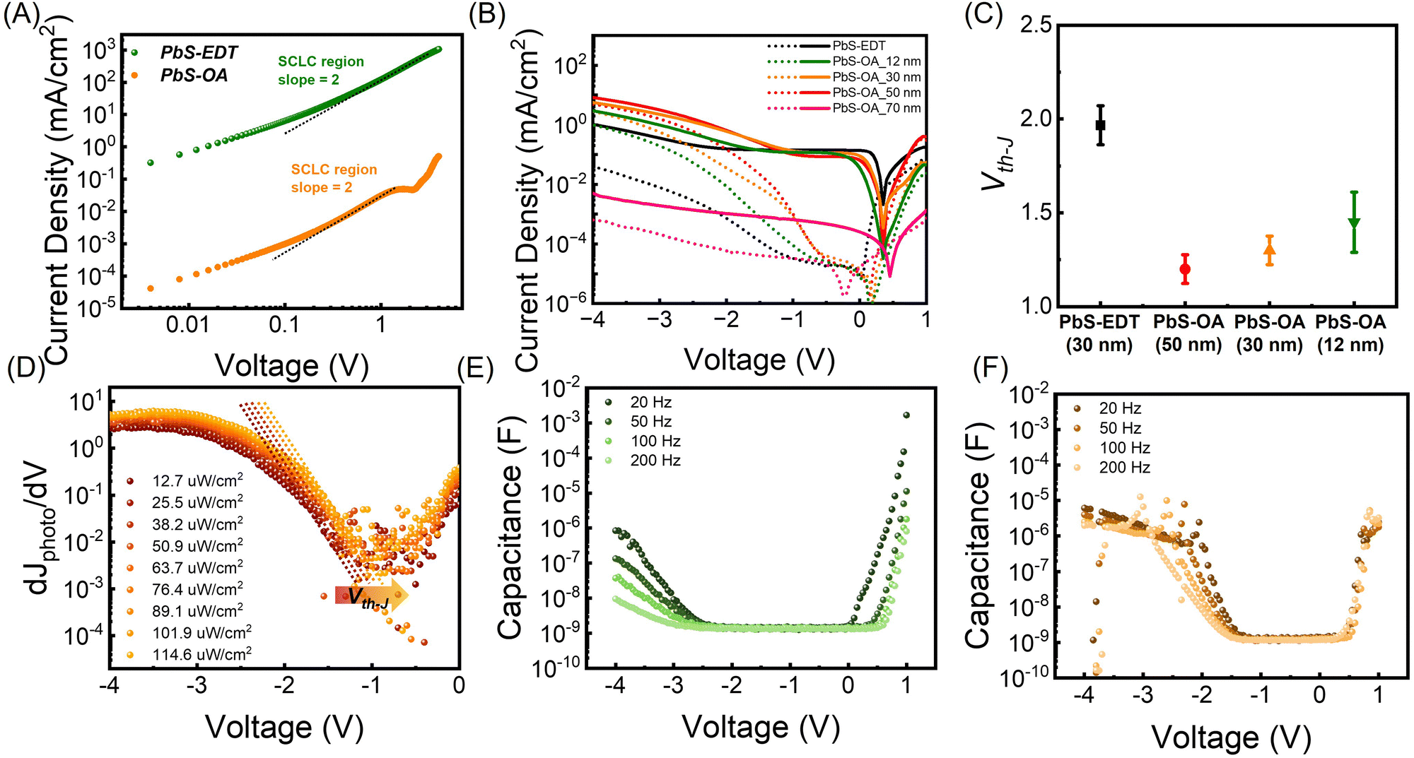 | ||
| Fig. 3 (A) Space charge limited current (SCLC) results of PbS-EDT and PbS-OA hole-only devices. (B) J–V curves of PDs with PbS-EDT and PbS-OA (12, 30, 50, 70 nm) under dark and 980 nm laser illumination with a 130 μW cm−2 intensity, and the (C) calculated Vth-J. (D) dJphoto/dV–V curve of PD with PbS-OA (30 nm) measured under different light intensities. Frequency dependent C–V curves of the PbS QPD using (E) PbS-EDT (30 nm) and (F) PbS-OA (30 nm) as HTLs. | ||
To measure the effect of different HTL layers on the device performance, ITO/ZnO-pristine/PbS-halide/PbS-EDT/Au (PD with PbS-EDT) and ITO/ZnO-pristine/PbS-halide/PbS-OA/Au (PD with PbS-OA) photodiodes with varying PbS-OA thickness (12, 30, 50, and 70 nm) were prepared. J–V characteristics of the PD with PbS-EDT and PbS-OA are shown in Fig. 3B. Below the Vth-J of the PD (−1.3 V), the PD with PbS-OA shows a lower illuminated current density value compared to the PD with PbS-EDT because the low hole mobility of the PbS-OA hinders the extraction process of photogenerated hole carriers (Fig. S6, ESI†). In contrast, above the Vth-J, the PD with 12, 30, and 50 nm PbS-OA exhibited a large photomultiplication effect and achieved a higher illuminated current density than that with PbS-EDT. As PbS-OA has low hole mobility, holes are accumulated in this layer, inducing band-bending and subsequently tunneling under high voltage. As PbS-OA is the most insulating layer in the PD, the voltage drop occurs in PbS-OA, inducing high electric fields above 2.5 × 10⁸ V cm−1. Therefore, despite the low hole mobility in PbS-OA, the charge transport by tunneling between OA-capped PbS QDs is allowed under high voltage, leading to a huge photocurrent density.
As the thickness of PbS-OA increases from 12 to 50 nm, more charges accumulate, leading to higher band bending-induced tunneling currents. At a thickness of 12 nm, the charge accumulation is low so that band bending-induced tunneling is low, leading to low photomultiplication. At a thickness of 50 nm, an excessive number of carriers are accumulated, leading to an excessively high dark current. As a result, the photo/dark current ratio is low, as discussed in detail in Fig. S7 (ESI†). Therefore, the PD with PbS-OA is optimized with a PbS-OA thickness of 30 nm. Notably, when the PbS-OA is too thick (above 70 nm), this layer becomes completely insulating. As band bending occurs only at the interface and the main body of PbS-OA is insulating, tunneling is not allowed, yielding low dark current and photocurrent, as seen in Fig. 3B and Fig. S8A (ESI†).
To further investigate the photomultiplication, thickness, light intensity, and temperature dependent electrical measurements were performed. As seen in Fig. 3C, Vth-J of PD with PbS-OA is inversely proportional to the thickness of PbS-OA, this indicates that the more hole carriers accumulated by thicker PbS-OA accelerate the tunneling and photomultiplication phenomena. The thickness of PbS-OA was optimized as 30 nm, as detailed in Fig. S7 and Note S2 (ESI†). In addition, Vth-J gradually decreases as temperature increases (Fig. S8B, ESI†). At higher temperature, the mobility difference becomes extended in coincide with the great increment of mobility of PbS-halide, enhancing hole carrier accumulation. As the intensity of light increases, Vth-J is decreased and this also can be rationalized as that a larger amount of photogenerated carriers assist hole accumulation (Fig. S8C, ESI† and Fig. 3D). These analyses strongly support that hole mobility difference induced charge accumulation and band bending in the HTL leads to large photomultiplication.
The charge accumulation in PD with PbS-EDT and PbS-OA was measured using a frequency dependent C–V curve from −4 V to 1 V from 20 Hz to 200 Hz (Fig. 3E and F). From these results, we calculated the changes of Vth-C by detecting frequency. In the case of PD with PbS-EDT, the measured capacitance at the accumulation region significantly decreased, and its Vth-C changed from −1.9 V to −2.5 V as the applied frequency increased from 20 Hz to 200 Hz (Fig. S9A, ESI†). This large frequency-dependent capacitance shift in this low frequency range (<103 Hz) describes the origin of ETL-assisted carrier accumulation as deep interfacial defect states caused by humidity treatment.36 In contrast, Vth-C of PD with PbS-OA exhibited a frequency independent behavior in this range, which changed minimally at −1.3 V (Fig. S9B, ESI†).
Fig. 4A shows the structure of our PM-QPD designed via a double photomultiplication strategy. In Fig. 4B, the PD mode (mode I) and PM mode (mode II) are commonly observed below and above the Vth, respectively. Below Vth, PM-QPD exhibited photodiode behaviors, including no dramatic photocurrent density increase with an increase in the reverse voltage value. In contrast, above Vth (mode II), sufficient voltage is applied, and charge-accumulation and tunneling occur, leading to photomultiplication. In Fig. 4C, the J–V curves of PM-QPD monitored under a dark state and various intensities of 980-nm-light are shown. A rapid increase in the photocurrent density and photomultiplication effect occurred above Vth, which is attributed to the band bending induced tunneling and carrier multiplication under high voltage and electrical field. We observed two clearly divided regions of mode I and mode II. In Fig. 4D, PM-QPD exhibited constant EQE as the reverse bias increased in mode I (0 to −2 V), whereas the EQE rapidly increased above 105% in mode II (−2 to −10 V).
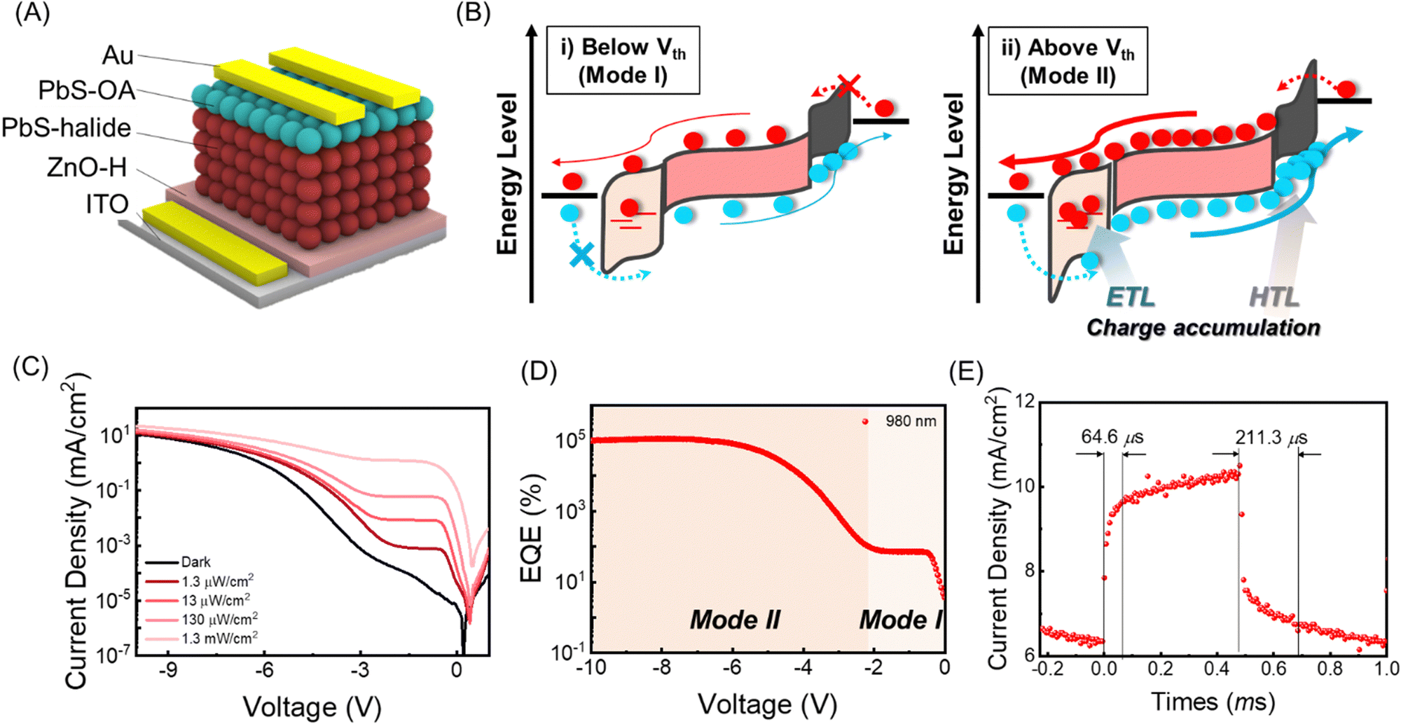 | ||
| Fig. 4 (A) Schematic of the PM-QPD structure and (B) charge accumulation assisted photomultiplication mechanism of PM-QPD. (C) J–V curve of PM-QPD under a 980 nm laser with varying light intensity from 1.3 μW cm−2 to 1.3 mW cm−2. (D) EQE versus voltage graph under 980 nm with an intensity of 1.3 μW cm−2. (E) Response speed of PM-QPD at a −10 V bias. | ||
To further analyze the operating mechanisms of mode I and mode II, we replotted the photocurrent density versus light intensity curves in Fig. S10 (ESI†). In mode I, PM-QPD shows linear growth (Jph ∝ Pn, n ≅ 1) with the incident optical power, n = 1.03 at −1 V, implying that photogenerated carriers were extracted by the built-in potential. On the other hand, in mode II, PM-QPD shows sublinear growth (Jph ∝ Pn, n < 1) with the incident power, n = 0.31 at −10 V. These low n values reveal a strong photogain effect and dominant contribution of photogating to the total photocurrent generation, where photoexcited carriers are trapped in localized states and generate a local electric field.37 In addition, using a 1 kHz laser pulse, the response time of PM-QPDs was measured at −1 V, −4 V, and −10 V. The rise-time was measured from 10% to 90% of the highest value, and the fall-time was conversely measured from 90% to 10%. Compared to other types of photomultiplication devices such as phototransistors (>10 ms),38,39 our PM-QPD exhibited a faster response speed with rise- and fall-times of 12.8 μs/28.8 μs at −1 V (mode I), 28.8 μs/100 μs at −4 V, and 64.6 μs/211.3 μs at −10 V (mode II) (Fig. S11, ESI† and Fig. 4E). More detailed characterization regarding device stability is presented in Fig. S12 (ESI†).
To quantitatively measure the performance of the PM-QPD, the calculated EQE spectrum is depicted in Fig. S13 (ESI†). In mode I, regardless of the wavelength, PM-QPD exhibited an EQE below 102%. On the other hand, as the applied bias increased in mode II, the EQE of PM-QPD was largely multiplied and reached 105% above a bias of −8 V. Above −10 V, PM-QPD was largely deformed and lost its performance. Record performance was achieved at −10 V with responsivity of 7.84 × 10² A W−1 and EQE of 1.46 × 10⁵%. These are the highest responsivity and EQE values (>105%) among previously reported PM-QPDs, which were obtained by chemical treatment of ZnO and the utilization of QDs with long ligands (Table S1, ESI†).
Conclusions
We developed an efficient PM-QPD using a double photomultiplication strategy. Through humidity treatment, we precisely controlled the interfacial defect density on the ETL, thereby accumulating electron carriers. Contrary to the conventional thoughts, long-chain OA ligand passivated CQDs were used as the HTL and induced a large carrier mobility difference and triggered hole-carrier accumulation, resulting in a large photomultiplication effect. These charge accumulations were further investigated using capacitance and current–voltage measurements. The fabricated PM-QPD exhibited two distinct operation modes, the PD and PM modes. At PM modes, they reported the ultra-high EQE of 1.46 × 10⁵% under 980 nm. This photomultiplication effect can be applied to advanced future technologies such as quantum communication, which requires the detection of signal photons under ambient conditions.Experimental
Materials
Ammonium acetate (NH4Ac), lead(II) oxide (PbO) (99.999%), zinc acetate dihydrate, lead(II) iodide (PbI2), oleic acid (OA) (90%), lead(II) bromide (PbBr2), potassium hydroxide (KOH), bis(trimethylsilyl)sulfide (TMS2) (98%), n-octane (99%), dimethylformamide (DMF), 1-octadecene (ODE) (90%), 1,2-ethanedithiol (EDT) (98%), butylamine, and acetonitrile were purchased from Sigma-Aldrich Co. All reagents were used without further purification.Synthesis of ZnO NPs and PbS QDs
ZnO NPs were synthesized using a slightly modified method from a previous study.40 The Zn precursor was prepared by dissolving zinc acetate dihydrate (2.95 g) in methanol (125 mL) and heating the solution to 60 °C. A KOH solution (1.48 g in 65 mL of methanol) was slowly injected into the Zn precursor. The mixture was stirred at 60 °C for 2.5 h and then cooled to room temperature. The obtained ZnO NPs were purified thrice using pure methanol. Purified ZnO NPs were collected in chloroform (70 mg mL−1).PbS QDs were synthesized using a previously reported hot-injection method.22 A solution of OA (3 mL), PbO (0.9 g), and ODE (20 mL) was degassed in a 100 mL three-neck flask for 2 h at 110 °C. Next, the solution was heated to 120 °C under a nitrogen atmosphere. The sulfur precursor (240 μL of TMS2 in 8 mL of ODE) in a 10 mL syringe was injected into the flask and then cooled to room temperature via natural cooling. The synthesized QDs were purified three times using acetone and ethanol. Finally, the QDs were dispersed in octane (50 mg mL−1).
A solution exchange process was conducted to cap the PbS QDs with lead halide ligands using a previously reported method with slight modifications.41 Lead halides (0.46 g of PbI2 and 0.07 g of PbBr2) and NH4Ac (0.03 g) were dissolved in DMF (10 mL). Subsequently, the synthesized QDs (10 mL, 10 mg mL−1) were vigorously mixed with the DMF solution for 2 min. The ligand-exchanged QD solution was washed three times with octane and centrifuged in toluene. The precipitated QDs were collected using butylamine (200 mg mL−1).
Fabrication of the NIR photodetector
ITO-deposited glass was sequentially cleaned with acetone, isopropanol, and deionized water for 5 min via sonication. The ITO glass was then treated with UV-ozone for 20 min and spin coated with ZnO NPs at 2500 rpm for 30 s under dry conditions. To obtain a dense ZnO layer, a ZnO thin film was annealed for 10 min at 80 °C (ZnO-pristine). For humidity treatment, the ZnO-pristine thin film was placed in a humidity chamber (relative humidity >80%) for 1 h. The solution-exchanged PbS QDs were then spin-coated onto the ZnO thin film at 2500 rpm for 30 s. Next, the PbS-OA layer was deposited by spin-coating with the as-synthesized OA-capped PbS QDs at 2500 rpm for 30 s for the fabrication of a 30-nm-thick PbS-OA layer. The PbS-EDT layer was deposited using the solid exchange method. An EDT solution (0.02 vol% in acetonitrile) was applied to the OA-capped PbS QD films for 30 s to exchange the ligands. The films were washed three times with acetonitrile to eliminate residues from the ligand exchange process. A 100-nm-thick Au top electrode was deposited on the hole transport layers via thermal evaporation. The area of the device was 4 mm2.Characterization
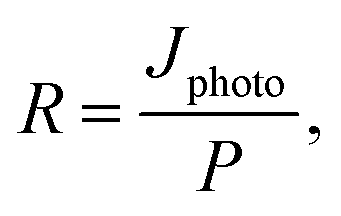
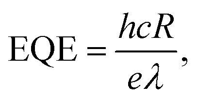
An LCR meter (model 4100, Wayne Kerr) and a probe station (MST-4000A, MSTECH) were used to measure the capacitance–voltage curve of the PbS QDPD. The current density–voltage characteristics were measured using a source meter (Keithley 2400, Tektronix). UV-Vis (Cary5000, Agilent Technologies) and FTIR (Model LabRam ARAMIS IR2, Horiba Jobin Yvon) spectroscopy techniques were used to analyze the optical properties of the ZnO NPs and PbS CQD thin films. In addition, a high-resolution transmission electron microscope (Tecnai G2 F30, FEI, Korea Basic Science Institute) was used to analyze the structures of the ZnO NPs and PbS CQDs. The local atomic structures of the ZnO NPs were evaluated using X-ray absorption spectroscopy. EQE spectra were obtained using a K3100 EQX quantum efficiency measurement system (McScience). Monochromated white light from a xenon lamp was mechanically chopped at a frequency of 300 Hz.To quantify the performance of the PM–QPDs, their responsivity (R) and EQE were calculated using the following equations:42,43
| Jphoto = Jilluminated − Jdark, | (1) |
 | (2) |
 | (3) |
Author contributions
Byung Ku Jung: conceptualization, methodology, formal analysis, investigation, writing – original draft, writing – review & editing. Taesung Park: conceptualization, methodology, visualization, Young Kyun Choi: formal analysis, writing – original draft, writing – review & editing. Yong Min Lee: methodology, data curation, Tae Hyuk Kim & Jae Won Shim: formal analysis and methodology. Seongkeun Oh: data curation, Yu-hwa Lo & Tse Nga Ng: writing – review & editing, supervision, project administration, Soong Ju Oh: conceptualization, methodology, investigation, writing – review & editing, supervision, project administration, funding acquisition.Conflicts of interest
The authors declare that they have no known competing financial interests or personal relationships that could have appeared to influence the work reported in this paper.Acknowledgements
This study was supported by the Technology Innovation Program (korea-led of K-Sensor technology for market leadership) (RS-2023-00256247) funded By the Ministry of Trade, Industry & Energy (MOTIE, Korea), (NRF-2018M3D1A1059001) Creative Materials Discovery Program through the National Research Foundation of Korea (NRF) funded by Ministry of Science and ICT, (2022R1A2C4001517) Basic Science Research Program through the National Research Foundation of Korea (NRF) funded by the Ministry of Science ICT and Future Planning, the National Research Foundation of Korea (NRF) grant funded by the Korean government (MSIT) (no. 2022R1A2C2009523), and Samsung Electronics Co., Ltd (IO201210-08027). T. N. N. and B. S. are supported by USA National Science Foundation award ECCS-2222203.References
- R. Sliz, M. Lejay, J. Z. Fan, M. J. Choi, S. Kinge, S. Hoogland, T. Fabritius, F. P. Garciá De Arquer and E. H. Sargent, ACS Nano, 2019, 13, 11988–11995 CrossRef CAS PubMed.
- B. K. Jung, H. K. Woo, C. Shin, T. Park, N. Li, K. J. Lee, W. Kim, J. H. Bae, J. P. Ahn, T. N. Ng and S. J. Oh, Adv. Opt. Mater., 2021, 2101611, 1–10 Search PubMed.
- N. Li, Y. S. Lau, Z. Xiao, L. Ding and F. Zhu, Adv. Opt. Mater., 2018, 6, 1–9 Search PubMed.
- J. P. Clifford, G. Konstantatos, K. W. Johnston, S. Hoogland, L. Levina and E. H. Sargent, Nat. Nanotechnol., 2009, 4, 40–44 CrossRef CAS PubMed.
- K. Yang, J. Wang, Z. Zhao, F. Zhao, K. Wang, X. Zhang and F. Zhang, Org. Electron., 2020, 83, 105739 CrossRef CAS.
- W. Zhou, Y. Shang, F. P. García de Arquer, K. Xu, R. Wang, S. Luo, X. Xiao, X. Zhou, R. Huang, E. H. Sargent, Z. Ning, L. Wu, R. R. Xu, G. Yao, D. Su, Z. Su, H. Yang, K. Yang, J. Wang, Z. Zhao, F. Zhao, K. Wang, X. Zhang, F. Zhang, K. Xu, L. Ke, H. Dou, R. R. Xu, W. Zhou, Q. Wei, X. Sun, H. Wang, H. Wu, L. Li, J. Xue, B. Chen, T. C. Weng, L. Zheng, Y. Yu, Z. Ning, Z. Zhao, J. Wang, C. Xu, K. Yang, F. Zhao, K. Wang, X. Zhang and F. Zhang, Org. Electron., 2020, 63, 366–373 Search PubMed.
- Z. Zhao, J. Wang, C. Xu, K. Yang, F. Zhao, K. Wang, X. Zhang and F. Zhang, J. Phys. Chem. Lett., 2020, 11, 366–373 CrossRef CAS PubMed.
- J. Zhang, M. A. Itzler, H. Zbinden and J. W. Pan, Light: Sci. Appl., 2015, 4, 1–13 CrossRef.
- Y.-L. Wu, K. Fukuda, T. Yokota and T. Someya, Adv. Mater., 2019, 31, 1903687 CrossRef CAS PubMed.
- A. Rogalski, Opto-Electron. Rev., 2012, 20, 279–308 Search PubMed.
- H. Aghasi, S. M. H. Naghavi, M. Tavakoli Taba, M. A. Aseeri, A. Cathelin and E. Afshari, Appl. Phys. Rev., 2020, 7, 21302 CAS.
- J. Kublitski, A. Fischer, S. Xing, L. Baisinger, E. Bittrich, D. Spoltore, J. Benduhn, K. Vandewal and K. Leo, Nat. Commun., 2021, 12, 4259 CrossRef CAS PubMed.
- J. Ahn, S. Jeon, H. K. Woo, J. Bang, Y. M. Lee, S. J. Neuhaus, W. S. Lee, T. Park, S. Y. Lee, B. K. Jung, H. Joh, M. Seong, J. H. Choi, H. G. Yoon, C. R. Kagan and S. J. Oh, ACS Nano, 2021, 15, 15667–15675 CrossRef CAS PubMed.
- J. Zhang, S. Zhang, Y. Zhang, O. A. Al-Hartomy, S. Wageh, A. G. Al-Sehemi, Y. Hao, L. Gao, H. Wang and H. Zhang, Laser Photonics Rev., 2022, 2200551 Search PubMed.
- M. Liu, N. Yazdani, M. Yarema, M. Jansen, V. Wood and E. H. Sargent, Nat. Electron., 2021, 4, 548–558 CrossRef.
- H. S. Gupta, A. S. K. Kumar, M. S. Baghini, S. Chakrabarti and D. K. Sharma, IEEE Photonics Technol. Lett., 2016, 28, 1673–1674 CAS.
- A. Bakulin, A. I. DSouza, C. Masterjohn, E. Mei, C. Li, E. Klem and D. Temple, Image Sensing Technologies: Materials, Devices, Systems, and Applications V, Proc. SPIE, 2018, 10656, 1065614 Search PubMed.
- E. H. Sargent, Nat. Photonics, 2012, 6, 133–135 CrossRef CAS.
- J. H. Song and S. Jeong, Nano Convergence, 2017, 4, 1–8 CrossRef PubMed.
- M. A. Hines and G. D. Scholes, Adv. Mater., 2003, 15, 1844–1849 CrossRef CAS.
- F. P. García de Arquer, D. V. Talapin, V. I. Klimov, Y. Arakawa, M. Bayer and E. H. Sargent, Science, 2021, 373, 6555 CrossRef PubMed.
- O. Voznyy, L. Levina, J. Z. Fan, M. Askerka, A. Jain, M. J. Choi, O. Ouellette, P. Todorović, L. K. Sagar and E. H. Sargent, ACS Nano, 2019, 13, 11122–11128 CrossRef CAS PubMed.
- D. Y. Kim, K. R. Choudhury, J. W. Lee, D. W. Song, G. Sarasqueta and F. So, Nano Lett., 2011, 11, 2109–2113 CrossRef CAS PubMed.
- J. Ahn, S. Jeon, W. S. Lee, H. K. Woo, D. Kim, J. Bang and S. J. Oh, J. Phys. Chem. C, 2019, 123, 18087–18094 CrossRef CAS.
- B. K. Jung, W. Kim and S. J. Oh, J. Korean Ceram. Soc., 2021, 58, 521–529 CrossRef CAS.
- N. Sukharevska, D. Bederak, V. M. Goossens, J. Momand, H. Duim, D. N. Dirin, M. V. Kovalenko, B. J. Kooi and M. A. Loi, ACS Appl. Mater. Interfaces, 2021, 13, 5195–5207 CrossRef CAS PubMed.
- A. R. Kirmani, A. D. Sheikh, M. R. Niazi, M. A. Haque, M. Liu, F. P. G. de Arquer, J. Xu, B. Sun, O. Voznyy, N. Gasparini, D. Baran, T. Wu, E. H. Sargent and A. Amassian, Adv. Mater., 2018, 30, 1801661 CrossRef PubMed.
- H. Choi, J. G. Lee, X. D. Mai, M. C. Beard, S. S. Yoon and S. Jeong, Sci. Rep., 2017, 7, 1–8 CrossRef PubMed.
- W. Zhou, Y. Shang, F. P. García de Arquer, K. Xu, R. Wang, S. Luo, X. Xiao, X. Zhou, R. Huang, E. H. Sargent and Z. Ning, Nat. Electron., 2020, 3, 251–258 CrossRef CAS.
- K. Xu, L. Ke, H. Dou, R. Xu, W. Zhou, Q. Wei, X. Sun, H. Wang, H. Wu, L. Li, J. Xue, B. Chen, T. C. Weng, L. Zheng, Y. Yu and Z. Ning, ACS Appl. Mater. Interfaces, 2022, 14, 14783–14790 CrossRef CAS PubMed.
- J. Poppe, S. Gabriel, L. Liebscher, S. G. Hickey and A. Eychmüller, J. Mater. Chem. C, 2013, 1, 1515–1524 RSC.
- Y. Lin, M. Li, J. Xia, H. Ding, L. Xu, X. Yang and S. Li, Cellulose, 2021, 28, 4211–4222 CrossRef CAS.
- A. Barroso-Bogeat, M. Alexandre-Franco, C. Fernández-González and V. Gómez-Serrano, Arabian J. Chem., 2019, 12, 3963–3976 CrossRef CAS.
- J. Ke, X. Li, Q. Zhao, Y. Hou and J. Chen, Sci. Rep., 2014, 4, 4–9 Search PubMed.
- Y. Cho, B. Hou, J. Lim, S. Lee, S. Pak, J. Hong, P. Giraud, A. R. Jang, Y. W. Lee, J. Lee, J. E. Jang, H. J. Snaith, S. M. Morris, J. I. Sohn, S. Cha and J. M. Kim, ACS Energy Lett., 2018, 3, 1036–1043 CrossRef CAS PubMed.
- M. Salado, L. Contreras-Bernal, L. Caliò, A. Todinova, C. López-Santos, S. Ahmad, A. Borras, J. Idígoras and J. A. Anta, J. Mater. Chem. A, 2017, 5, 10917–10927 RSC.
- H. Fang and W. Hu, Adv. Sci., 2017, 4, 1700323 CrossRef PubMed.
- H. Lee, J. Ahn, S. Im, J. Kim and W. Choi, Sci. Rep., 2018, 8, 1–7 Search PubMed.
- J.-H. Kim, B. K. Jung, S.-K. Kim, K.-R. Yun, J. Ahn, S. Oh, M.-G. Jeon, T.-J. Lee, S. Kim, N. Oh, S. J. Oh and T.-Y. Seong, Adv. Sci., 2023, 10, 2207526 CrossRef CAS PubMed.
- H. K. Woo, M. S. Kang, T. Park, J. Bang, S. Jeon, W. S. Lee, J. Ahn, G. Cho, D. K. Ko, Y. Kim, D. H. Ha and S. J. Oh, Nanoscale, 2019, 11, 17498–17505 RSC.
- J. Z. Fan, N. T. Andersen, M. Biondi, P. Todorović, B. Sun, O. Ouellette, J. Abed, L. K. Sagar, M. J. Choi, S. Hoogland, F. P. G. de Arquer and E. H. Sargent, Adv. Mater., 2019, 31, 1–8 Search PubMed.
- F. P. García De Arquer, A. Armin, P. Meredith and E. H. Sargent, Nat. Rev. Mater., 2017, 2, 16100 CrossRef.
- C. Li, W. Huang, L. Gao, H. Wang, L. Hu, T. Chen and H. Zhang, Nanoscale, 2020, 12, 2201–2227 RSC.
- Y. Fang, A. Armin, P. Meredith and J. Huang, Nat. Photonics, 2019, 13, 1–4 CrossRef CAS.
Footnotes |
| † Electronic supplementary information (ESI) available. See DOI: https://doi.org/10.1039/d3nh00456b |
| ‡ B. K. J. and T. P. contributed equally to this study. |
| This journal is © The Royal Society of Chemistry 2024 |