
Local modulation of Au/MoS2 Schottky barriers using a top ZnO nanowire gate for high-performance photodetection†
Yu
Xiao
 a,
Guisheng
Zou
a,
Jinpeng
Huo
a,
Tianming
Sun
ab,
Jin
Peng
a,
Zehua
Li
a,
Daozhi
Shen
c and
Lei
Liu
*a
a,
Guisheng
Zou
a,
Jinpeng
Huo
a,
Tianming
Sun
ab,
Jin
Peng
a,
Zehua
Li
a,
Daozhi
Shen
c and
Lei
Liu
*a
aDepartment of Mechanical Engineering, State Key Laboratory of Tribology, Key Laboratory for Advanced Manufacturing by Materials Processing Technology, Ministry of Education of PR China, Tsinghua University, Beijing 100084, P. R. China. E-mail: liulei@tsinghua.edu.cn
bCollege of Materials Science and Engineering, Taiyuan University of Technology, Taiyuan 030024, Shanxi Province, China
cSchool of Mechanical Engineering, Shanghai Jiao Tong University, Shanghai, 200240, China
First published on 28th November 2023
Abstract
Schottky junctions are commonly used for fabricating heterojunction-based 2D transition metal dichalcogenide (TMD) photodetectors, characteristically offering a wide detection range, high sensitivity and fast response. However, these devices often suffer from reduced detectivity due to the high dark current, making it challenging to discover a simple and efficient universal way to improve the photoelectric performances. Here, we demonstrate a novel approach for integrating ZnO nanowire gates into a MoS2–Au Schottky junction to improve the photoelectric performances of photodetectors by locally controlling the Schottky barrier. This strategy remarkably reduces the dark current level of the device without affecting its photocurrent and the Schottky detectivity can be modified to a maximum detectivity of 1.4 × 10¹³ Jones with −20 V NG bias. This work provides potential possibilities for tuning the band structure of other materials and optimizing the performance of heterojunction photodetectors.
New conceptsThis manuscript proposes a new approach using top ZnO nanowire gates to successfully realize 1D gate integration in an Au–MoS2 Schottky photodetector to improve its photodetection performances. Most existing studies use a metal-based back gate or top gate to control performances. However, the back gate can easily suppress photogenerated carriers, and its control over the Schottky junction may be electrostatically shielded by the metal electrodes, while the top gate may block the incident light intended for the detection capabilities of the device and the fabrication process is accompanied by complex deposition procedures. This new gate configuration successfully solves all the above problems. The ZnO nanowire gate has almost no effect on the reception of incident light signals and the effect of the gate is highly localized at the Schottky regions. Hence, only one single nanowire is needed to tune the device performance and this nanowire can solve the problems of high dark current and low detectivity of Schottky-based photodetectors. The proposed novel concept proves to be simple and efficient, and this general method provides references for performance optimization of other photodetectors based on a Schottky junction. In addition, this work also reveals a promising pathway for situations where localized control of the band structure is required. |
Introduction
Two-dimensional materials have been widely studied due to their unique electrical and optical properties,1,2 which can be applied to field effect transistors,3,4 logic devices,5,6 light-emitting diodes,7,8 photodetectors,9,10etc. Among them, MoS2 is a typical transition metal dichalcogenide for photodetectors with a good photoresponse and broadband photodetection range.11,12 To further improve the photoelectric performance of the device, different MoS2 heterostructures13–16 have been fabricated to increase the efficiency of photo-excited carrier generation. In these heterostructures, a Schottky junction between the metal and semiconductor is a simple and commonly used structure.17,18 A Schottky barrier can extend the detection range of the photodetector19 and the Schottky-based devices often exhibit high sensitivity and fast response compared with other heterostructure devices.20 Nevertheless, because of the properties of Schottky contacts, these devices usually encounter issues including high dark current, low detectivity, slow response speed, etc.21,22 Hence, finding a way to improve device performances is of considerable importance.Since MoS2 is an n-type semiconductor, applying negative bias to gates can effectively suppress its dark current.23,24 However, for the aforementioned devices based on Schottky junctions, the structure with a top film and several bottom electrodes is most commonly used25–27 to expose the junction to the incident light, which impedes the implementation of gate structures. The application of a back gate results in its control over the Schottky junction being electrostatically shielded by the bottom metal electrodes,28,29 which inhibits the effectiveness of gate modulation. Conversely, the use of a top gate may block the incident light intended for the detection capabilities of the device.30 Some studies offer solutions to this quandary, such as using materials with high transparency for top gates31,32 or using transparent materials for top electrodes,33,34 but the fabrication methods of these schemes are complex and involve fussy deposition processes. Therefore, it is important to propose a convenient and efficient method to solve the above problems.
Here, we demonstrate a BN-encapsulated MoS2-on-Au Schottky junction controlled by a ZnO top nanowire gate (NG) with a wide detecting range, high ON/OFF ratio of light response and ultrahigh detectivity. The ZnO NG is positioned directly above the Schottky junction to control the barrier at the Schottky interface. This gate will not block any incident light and its control over the junction will not be shielded by the Au electrodes. The influence of the NG is highly localized at the interface, thereby greatly reducing the dark current of the device with minimal change in the photocurrent by adjusting NG bias. This characteristic gives NGs unique advantages in improving photoresponse performances. In our experiments, the Schottky-based photodetectors can detect light in a wide spectrum ranging from 490 nm to 800 nm, and the device performance of the photodetectors will be greatly improved when −20 V bias is applied to the NG. The device exhibits an enhancement in the overall ON/OFF ratio of light response by over two orders of magnitude, and the detectivity can be improved to a maximum detectivity of 1.4 × 10¹³ Jones with −20 V NG bias when the incident wavelength is 525–625 nm and the light power is 0.1mW cm−2, which marks a significant level among the reported MoS2-based Schottky photodetectors (Table S1, ESI†). This work shows a novel approach for locally tuning the Schottky barrier and improving the performances of Schottky photodetectors with nanowire gates. Marked by its simplicity, efficiency, and high degree of localization, this strategy can provide potential possibilities for the tuning of band structure of low-dimensional materials and the performance optimization of heterojunction photodetectors.
Results and discussion
Fig. 1a shows a schematic of the Au–MoS2 Schottky junction with ZnO nanowires as NGs. Cr/Au was first deposited on the Si/SiO2 substrate as the electrode with 25 nm thickness and mechanically exfoliated MoS2 and h-BN were then transferred to the electrode successively as shown in Fig. S1 (ESI†). The Au electrode with a large work function will form a Schottky barrier at the Au–MoS2 interface with a high barrier height.35Fig. 1b shows the optical microscope image of the junction. To better understand the effect of different NGs on the Schottky performances, two different ZnO nanowires were placed on the source and drain side of the Au–MoS2 junction, respectively. During the test, the right Au–MoS2 side serves as the drain while the left side serves as the source. Atomic force microscopy (AFM) was used to study the thickness of Au–MoS2, h-BN and ZnO in this experiment. As shown in Fig. 1c and d, after being encapsulated with h-BN, the upper surface maintains good flatness. Detailed sizes (the diameter or the thickness) of the left ZnO, right ZnO, MoS2 and h-BN used in this junction are measured as 195 nm, 98 nm, 28 nm and 34 nm, respectively, as shown in Fig. 1e and Fig. S2 (ESI†).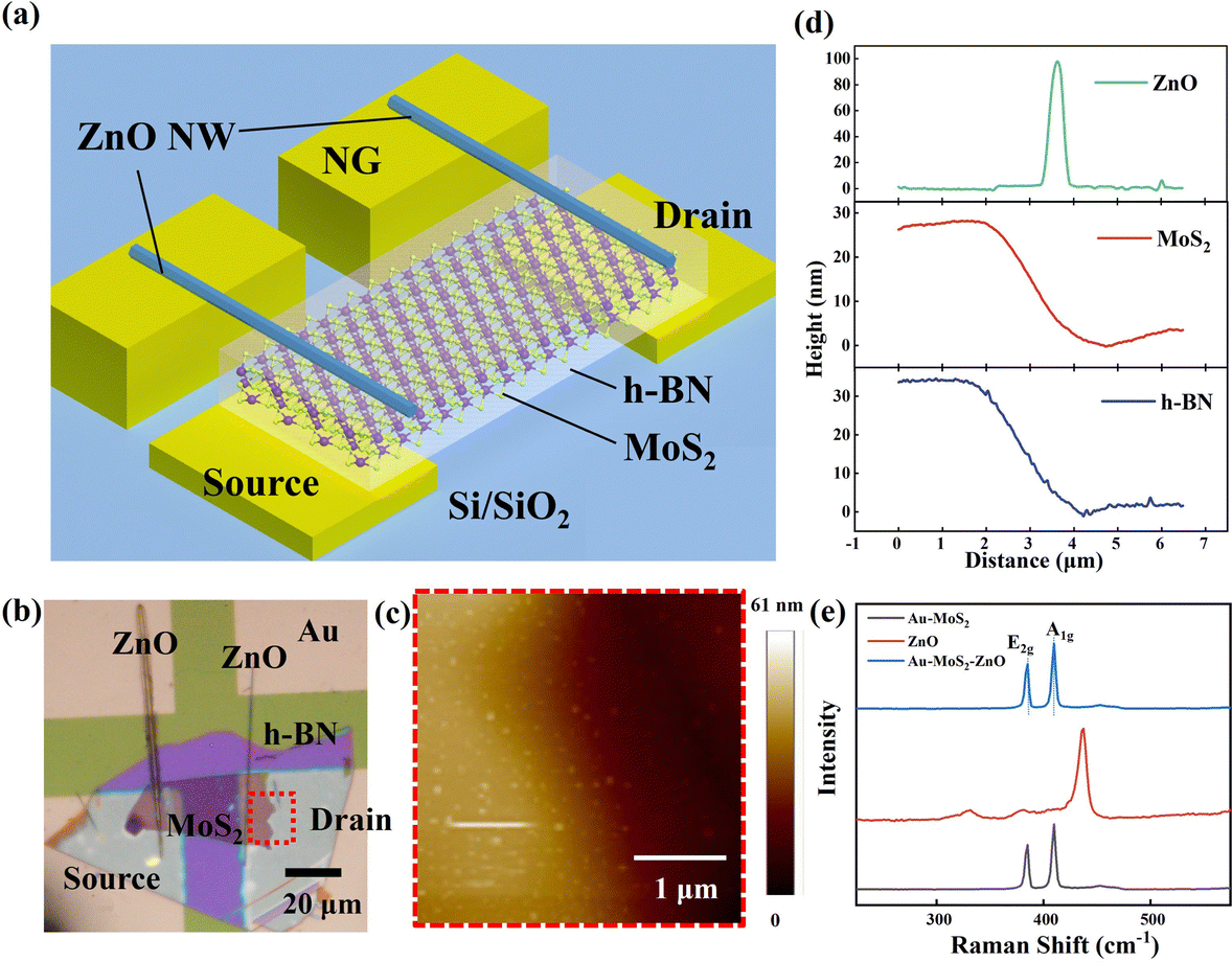 | ||
| Fig. 1 Schematic of the Schottky structure with top nanowire gates. (a) A schematic diagram of the Au–MoS2 Schottky junction with ZnO nanowires as NGs. (b) Optical image of the BN-encapsulated Au–MoS2 Schottky junction. (c) AFM topography mapping of the Au–MoS2 Schottky junction in the red dashed box of Fig. 1b. (d) AFM height profile of different materials in Fig. 1b. (e) Raman spectra of different substances used in the junction. | ||
Raman spectroscopy was used to show defects in 2D materials which determines the material quality. Fig. 1e shows the Raman spectra of different parts of MoS2 in 1b using a 532 nm excitation 1 μm laser spot. When the spot irradiated the Au–MoS2 junction, we observed strong peaks of an in-plane E2g mode near 383 cm−1 and an out-of-plane A1g mode near 409 cm−1, which ensures the quality of the MoS2 flake.36,37 It is worth noting that when we directly irradiated the laser spot on the ZnO nanowire above the Au–MoS2 junction as shown in Fig. S3 (ESI†), we obtain similar Raman signals as the case without ZnO nanowires and the Raman signals from the ZnO nanowires cannot be detected. By using the same batch of ZnO nanowires for networks, a stable Raman signal and a peak of 437 cm−1 was obtained in Fig. 1e and this shows that the ZnO nanowires have good properties.38 This phenomenon indicates that under these conditions, the existence of ZnO nanowires is “ignored” by the detection laser. This phenomenon displays an important property of the NG and this can be the solution of the Schottky junction gate problem mentioned above, which will be discussed later.
Fig. 2a1 shows the schematic of the Au–MoS2 Schottky photodetector without any NG bias and this structure as a comparison is conducive to the effective analysis of the NG structure performances in Fig. 2a2. Fig. 2b displays the I–V characterization to determine the charge separation in the Au–MoS2 junction in a dark environment. The dark current is about 5 nA at 1 V bias and 90 pA at −1 V bias due to the Au–MoS2 Schottky barrier. The difference in the current level under positive and negative bias may be due to the different contact states between the two sides of the device during the manufacturing process. As shown in Fig. S4 (ESI†), the effective photodetecting area of the Au–MoS2 structure on the left is smaller than that on the right, indicating that the well-contacted areas of the left structure are fewer than those of the right structure. This may lead to a high Schottky barrier on the left and further results in the relatively low current level on this side.
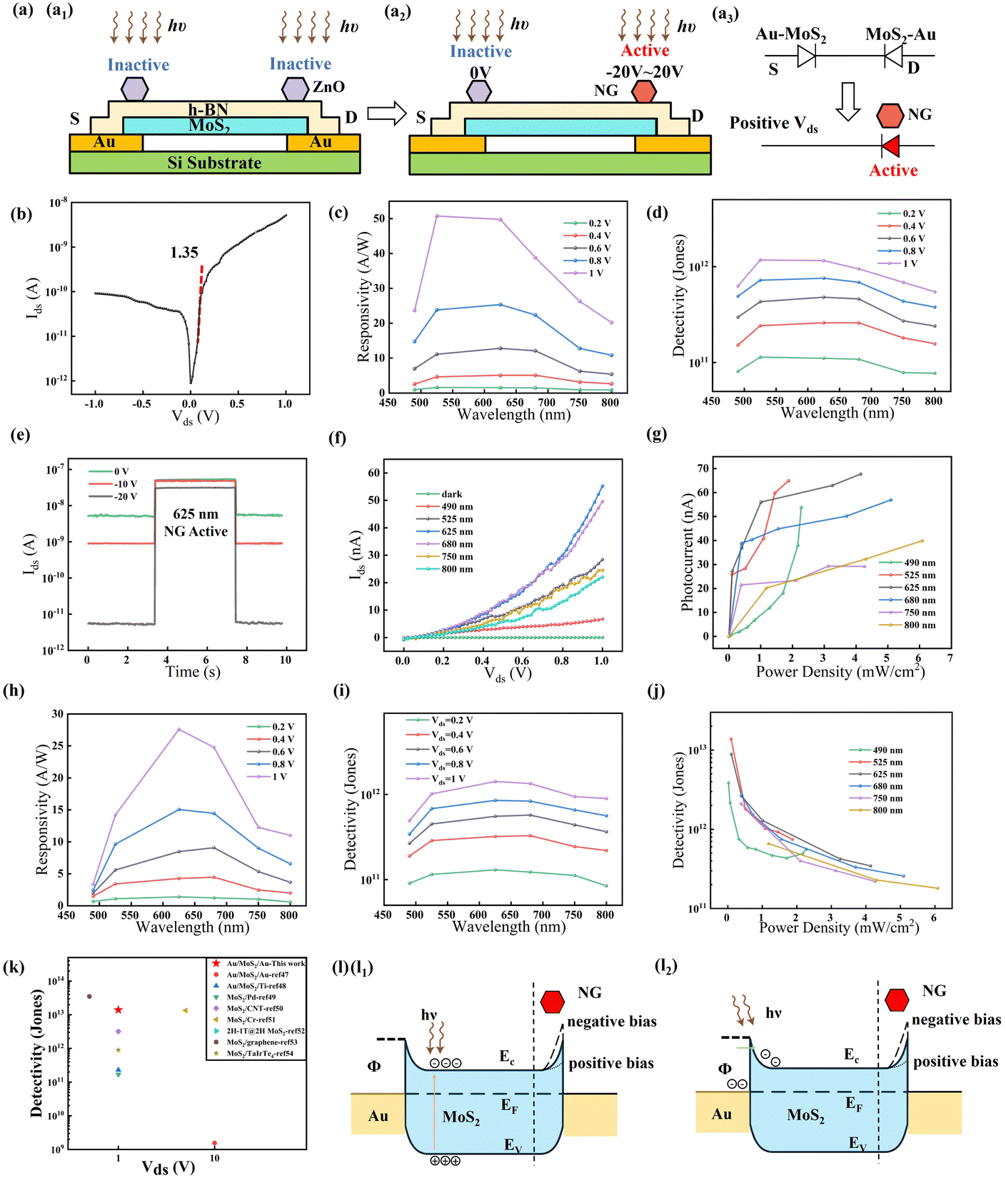 | ||
| Fig. 2 The photodetection performances of the Au–MoS2 Schottky junction. (a) A schematic of the Schottky photodetector exposed to light: (a1) without NG bias; (a2) with active ZnO NG bias; (a3) A schematic diagram of an active NG for influencing the corresponding Schottky. (b) I–V curves of the Au–MoS2 Schottky photodetector under dark conditions. (c) Responsivity and (d) detectivity of the device under illumination with different wavelengths without NGs. (e) The Schottky photodetector exposed to light at 625 nm with different NG bias. (f) Ids–Vds curves of the Au–MoS2 Schottky junction under illumination at different wavelengths of 1 mW cm−2 when −20 V bias is applied to NG. (g) The photoresponse of the junction at 1 V bias under illumination with different power densities when −20 V bias is applied to NG. (h) Responsivity and (i) detectivity of the device under illumination with different wavelengths when −20 V NG bias is applied. (j) Detectivity under different power densities when −20 V NG bias is applied. (k) The detectivity of the device in this work compared with devices of similar types. (l) Band diagram of the MoS2–Au Schottky device under the control of NG and different modes for generating a photo-induced charge carrier: (l1) directly excited electrons in MoS2; (l2) excited electrons through photoemission. | ||
Based on thermionic emission theory,39,40 the I–V characteristic of the junction can be given by the equation:
 | (1) |
 | (2) |
When the device is exposed to light without NG bias in Fig. 2a1, photocurrent is detected when a bias is applied. It is worth noting that since the Schottky barriers are on either side of the Au–MoS2–Au device as shown in Fig. 2a3, applying positive or negative bias will activate the Schottky barrier at different locations. In order to make the test results comparable, positive Vds bias is applied in subsequent tests to activate the Schottky barrier on the corresponding side. It was found that when halogen light is applied, the device exhibits a broadband of photoelectric response (Fig. S5, ESI†). The response is relatively stable, and the response intensity remains basically unchanged after multiple light on/off cycles (Fig. S6, ESI†). These results show that the junction has good and stable photodetection performances.
Further tests were carried out to determine the performances at different wavelengths. The light of light emitting diodes (LEDs) with different wavelengths was focused onto the device and the different photodetection responses are shown in Fig. S7 (ESI†). Critical parameters such as spectral responsivity (Rλ) and detectivity (D*) are calculated by using the following equations to show the sensibility and efficiency of the detector:43,44
 | (3) |
 | (4) |
 | (5) |
In the subsequent results, the values of D* are all calculated results after considering PSDthermal and PSDshot. The results are displayed in Fig. 2c and d where the illumination power is kept at 0.1 mW cm−2. An obvious high responsivity of the Au–MoS2 junction is obtained in a wide wavelength range from 490 nm to 800 nm and the results show that the device exhibits the highest photoresponsivity of ∼50 A W−1 at 1 V bias under a wavelength at 525–625 nm. In our calculation, the shot noise is considered as the major component in total noise, and the detectivity of the device is as high as ∼1.1 × 10¹² Jones in the wavelength range of 525–625 nm in Fig. 2d.
To further improve the photodetection performances of the device, two ZnO nanowire gates are placed above two Au–MoS2 Schottky junctions using the method described in the Experimental section as shown in Fig. 2a2. Since the two junctions are symmetrical, only one side of the Schottky is activated (the red Schottky Barrier Diode) when the bias is applied to the device. In this case, the activated Schottky can be effectively controlled by applying the Vg to the NG on the corresponding side. In order to visually demonstrate the effect of NG bias applied, the change of the device current with the ON/OFF switch under incident light with a wavelength of 625 nm and power of 0.1 mW cm−2 is measured in Fig. 2e. When no NG bias is applied, a dark current of ∼5 nA and a light current of ∼52 nA can be detected when the light changes from the OFF state to the ON state under 1 V Vds bias. The response and recovery time are less than 0.2 ms in Fig. S8 (ESI†). As the negative NG bias is applied, the dark current of the device decreases significantly and when the NG bias reaches −20 V, the dark current is reduced to ∼5 pA. Notably, this condition has little effect on the light current in Fig. 2e. Under −20 V bias, the light current does not change by an order of magnitude, decreasing from ∼52 nA to ∼31 nA. Therefore, using this method, the ON/OFF ratio of the light response can be significantly improved. Under the above conditions, the ratio is increased from ∼10 at 0 V NG bias to ∼6 × 10³ at −20 V NG bias.
More tests are carried out to fully demonstrate Schottky photodevices with nanowire gates. Fig. 2f displays the IV curve under different wavelengths of LED irradiation when −20 V NG bias is applied. After the addition of nanowire gates, the device still maintains a good response to a wide range of band light of 490–800 nm. However, for different wavelengths, a negative NG voltage has different inhibition effects on the light current and Fig. 2g further illustrates this characteristic at different power levels. For the wavelength of ≤525 nm, the photocurrent decreases greatly, while for a wavelength of ≥680 nm, the photocurrent decreases less and this may be due to different sensitivity of the Schottky junction toward different wavelengths.45,46 In addition, based on the results of testing at −20 V gate bias, the linearity properties of the structure to different wavelengths are summarized as shown in Fig. S9 (ESI†). The Schottky structure shows good linearity when detecting light with 490 nm. When fitting the relationship Ip ∝ Pα, the coefficient α obtained is 0.99, which is close to (1) However, when the incident light is 525 nm, the linearity parameter α has dropped to 0.83, and when the incident light wavelength is increased to 625 nm, the parameter α further drops to 0.7. This may be caused by possible existing defects in MoS2 as mentioned in Fig. 2b and they will trap part of the photogenerated carriers, thus causing the current of the structure to increase slowly with the increase of the incident light power density. According to the above measurement results, combined with eqn (3)–(5), the photodetection performances with a light power of 1 mW cm−2 after the addition of the nanowire gates are displayed in Fig. 2h and i. Since the negative NG bias reduces the photocurrent response of the device, the responsivity in each band is reduced accordingly, and the maximum responsivity at 625 nm is reduced to 27 A W−1 when −20 V is applied to NG. Although the photocurrent decreases, the dark current decreases at a faster rate, which leads to an increase in the device ON/OFF ratio and detectivity. In the case of 680 nm light, the ON/OFF ratio is improved by more than two orders of magnitude, and the detectivity is improved from 9 × 10¹¹ Jones to 1.3 × 10¹² Jones. Fig. 2j further displays the photoresponse at different incident light powers. When the incident light power is 0.1 mW cm−2, the device has a maximum detectivity of 1.4 × 10¹³ Jones with −20 V NG bias while the maximum detectivity without NG bias is 7.5 × 10¹² Jones, as shown in Fig. S10 (ESI†). This shows that the ability of the device to detect weak signals in a noise environment is obviously enhanced by adding the corresponding active nanowire gates to the Schottky junction. Therefore, the addition of active nanowire gates may be an effective way to improve the photodetection performances of Schottky junctions, especially the light ON/OFF ratio and the detectivity. The modified detectivity of this photodetector with NG is also at a high level in the similar type of devices in Fig. 2k and Table S1 (ESI†).47–54
The contribution of nanowire gates towards improving the photodetection performance is shown in Fig. 2l. After the contact between Au and MoS2, the Schottky interface is formed and electrons need to overcome the Schottky barrier Φ when flowing from Au to MoS2. In addition, due to the bottom Au electrode and dry-transferring process, a van der Waals gap is formed between the electrode and the semiconductor, further impeding the flow of hot electrons. These factors cause the device to have a relatively low dark current when the Vds bias is applied.
When the junction is exposed to light, the different responses to a wide spectrum of light indicate two ways in which the structure generates photocurrent. One way is for photons to directly excite electrons in MoS2 from the valence band to the conduction band in Fig. 2l1,55,56 leading to photocurrent under a certain bias, and this excitation mode plays the leading role when the wavelength is 625 nm in the above experiment. The other is photoemission20,21 in Fig. 2l2. When light reaches the Schottky interface, electrons in Au can be excited through the Schottky barrier and form the photocurrent. This mode is obviously less efficient than the previous one, so the photoresponse is relatively poor. For example, light with a wavelength of 800 nm uses this excitation mode. In this work, the barrier height at the interface can be effectively controlled by using the corresponding active nanowire gate. When the device is in the dark environment, the carrier concentration is low and the overall current level is mainly determined by the Schottky barrier. When negative bias is applied to the NG, the interface barrier increases in Fig. 2l and carrier flow is impeded, which can significantly reduce the dark current level of the device. However, when the device is under illumination conditions, for the above two modes, the nanowire gate has almost no effect on directly excited electrons and a small effect on electrons excited by photoemission. Therefore, the influence of the NG on the photocurrent is small, which results in a substantial improvement in the integrated photoresponse performance of the device.
Fig. 3 shows that one important reason for the good photoinduced response of the Au–MoS2 devices with nanowire gates is that NGs have little effect on the light absorption of the materials. Although the nanowire gate is located above MoS2, almost all incident photons are received by the material. Fig. 3a shows the photocurrent generation at the Schottky junction when Vds is 1 V. The results show that the contact part of Au and MoS2 has the highest response intensity (the responsive part is basically the same as the contact part in Fig. S4, ESI†), while the response of the other parts of the device is basically negligible. This demonstrates that photogenerated charge carriers are mainly generated at the Schottky junction and this area in the scanning micrograph is considered as the effective photodetecting area of the device. During the test, although a ZnO nanowire is located above the Schottky structure (Fig. 1b), the optical response of the region below the nanowire is not affected. Therefore, the existence of nanowires has no effect on the absorption of photon and the photodetection performances of the device.
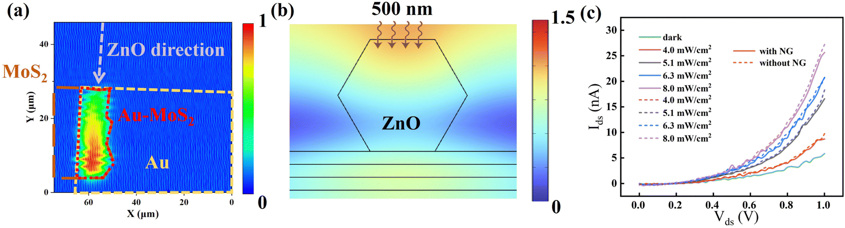 | ||
| Fig. 3 Influence of nanowire gates on the optical signal reception of devices. (a) Scanning normalized photocurrent micrograph of the Au–MoS2 device at Vds = 1 V. (b) A simulation of the distribution of the light field near the nanowire when the wavelength of incident light is 500 nm. (c) The photocurrent generated by the structure before and after placing ZnO nanowire gates under white light. | ||
Light with a wavelength of 500 nm is taken as an example to simulate the light field near the ZnO nanowire gates. Due to the small diameter of the nanowire, the energy of the incident light is gathered directly below the nanowire in Fig. 3b. The light diffracts at the nanowire causing some of the photons to bypass the nanowire and to be detected by MoS2 below. In addition, simulations of other wavelengths are carried out in Fig. S11 (ESI†) and parts of the light energy tend to concentrate below the ZnO nanowires. Therefore, locating the nanowire gates above the device does not block any incident light. To further illustrate this point, the same Schottky junction is tested with and without ZnO NGs under different light conditions in Fig. 3c. The photocurrent of the two cases are represented by solid and dotted lines respectively, and the figure shows the loss of photocurrent caused by using the nanowire gates is almost negligible.
Fig. 4 shows the localized affected regions of the nanowire gates. In previous explanations of the mechanism, the influence of the NG is considered to be limited in the regions of the Schottky junction. This demonstrates that the effect of the NG is highly localized. To illustrate this property, two gates are activated separately in Fig. 4a and b to observe their effect on electrical performances. When a certain bias is applied to the nanowires, the simulation results in Fig. 4c show that the most affected region of the electric field is directly below the base surface of the hexagonal prism ZnO. The highest potential is at the central axis and drops rapidly to be negligible along the direction of the membrane surface. The length of the region with a higher potential is even smaller than the diameter of the nanowires. This means that the field produced by the nanowire has a range of influences comparable to the diameter of the nanowire, and the affected regions are confined to the nanowire directly below. This simulation explains the localized effect of nanowires to a certain extent.
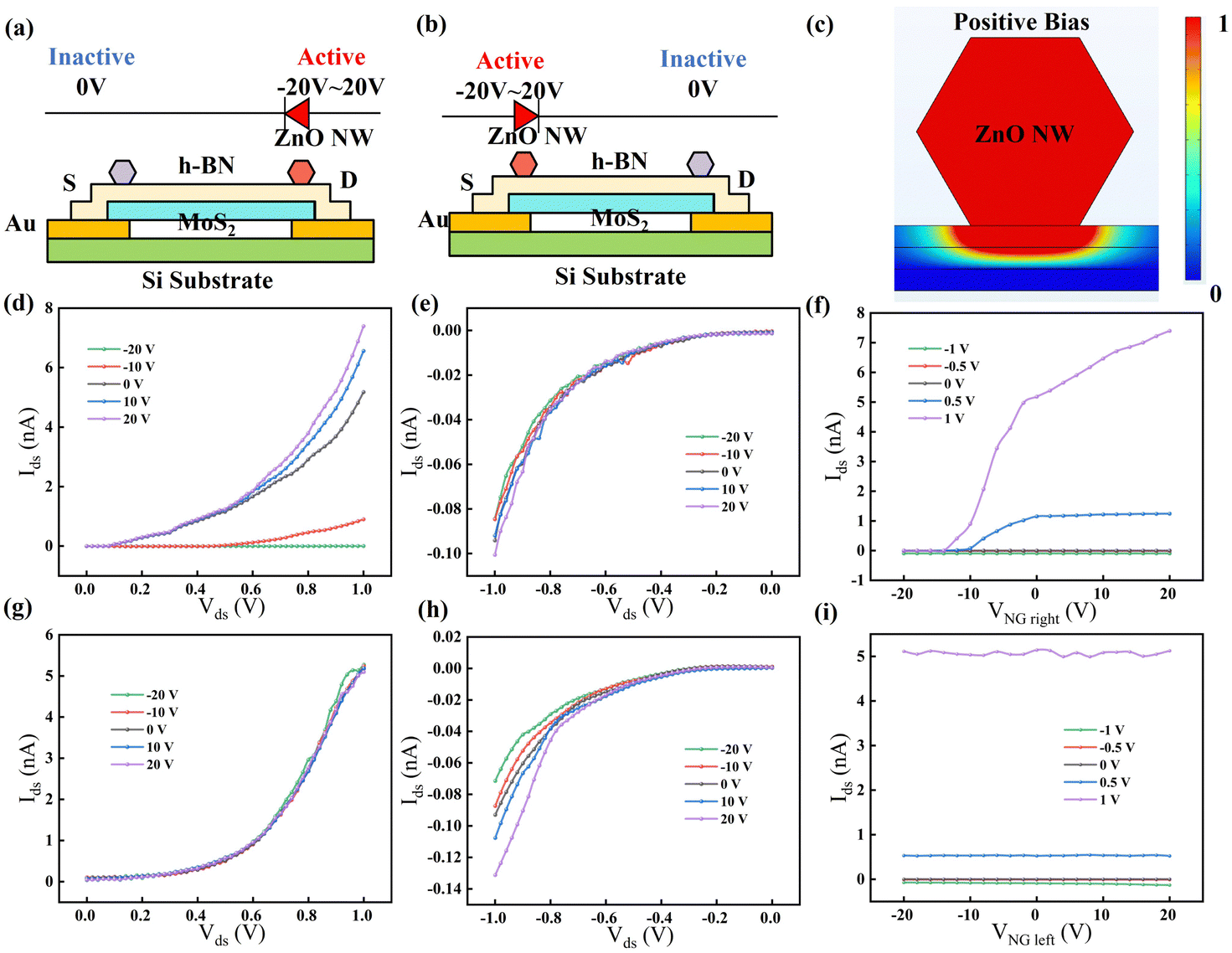 | ||
| Fig. 4 Localized tuning effect of NGs on the Au–MoS2 junction. (a) and (b) A schematic illustration of the Au–MoS2 structure when −20 V to 20 V bias is applied to the right NG (a) or the left NG (b) after adding ZnO nanowires to both sides. (c) A simulation of the potential distribution of the structure after bias is applied to the NG. (d) and (e) I–V curves of the devices after activating the NG shown in Fig. 3a when a positive (d) or negative (e) Vds bias is applied. (f) The transfer characteristics of the right NG. (g) and (h) −V curves of the devices after activating the NG shown in Fig. 3b when a positive (g) or negative (h) Vds bias is applied. (i) The transfer characteristics of the left NG. | ||
Because of the symmetry of the Au–MoS2–Au structure, only one side of the Schottky plays a dominant role when a positive or negative Vds voltage is applied. By activating the NG on the corresponding side, the Schottky can be controlled. When +1 V bias is applied, the electrons need to overcome the Schottky barrier on the right in Fig. 4a. At this time, by adjusting the voltage of the right gate, the current as shown in Fig. 4d can be obtained. As the gate bias drops from 20 V to −20 V, the response current drops from 7 nA to 4 pA. In contrast, when Vds is negative, the current is not controlled by this gate at all in Fig. 4e. This is also evident from the transfer curves in Fig. 4f. These results illustrate that the ZnO NG on the right only locally affects the Schottky below, and has no effect elsewhere. A similar conclusion is reached when the right NG changes to inactive and the left NG remains active. In contrast to the previous experiment, when a positive Vds is applied, the change in the left NG bias has no effect on the current in Fig. 4g, while when Vds is negative, the left NG controls the current between 0.07 nA and 0.13 nA in Fig. 4h. The results show that the device subjected to activation on the left nanowire exhibits a reduced gating effect and two possible reasons may cause this phenomenon. The first main reason is that the actual Schottky barrier heights on both sides are different due to the possible different contact states between the two sides as mentioned in Fig. 2b, which further leads to the asymmetry of the initial current levels. The second main reason is that the position of the left ZnO nanowire gate is deviated from the region where the Schottky mainly generates photocurrent, while the right nanowire is directly on the central region as shown in Fig. S12 (ESI†). The relatively weak gating effect on the left is due to the highly localized affected regions of the nanowire gate. Although the effect on the left side is relatively weak, it can still be found that the trend in electrical performance curves is consistent with that on the right side in Fig. 4i and Fig. S13 (ESI†), which demonstrates the effectiveness of the NG control for the Schottky structure. These results illustrate the mode of localized Schottky band control by NGs. After applying bias to NGs, the influence of NG only acts on the region and interface below the nanowire, but has no effect on most of the material and distant interfaces, which provides references for other possible works using nanowire gates.
Fig. 5a carries out experiments of the same device tuned by a back gate (BG) for comparison to further illustrate the special effect of adding nanowire gates. To make the comparison simple and convincing, the device is exposed to light at 625 nm of 0.1 mW cm−2. Different from the tuning mode of NG in Fig. 2, when the BG bias decreases from 20 V to −20 V, the photocurrent changes from 67 nA to 10 nA (Vds = 1 V) in Fig. 5b. The variation of the photocurrent under the tuning of BG is much greater than that of NG. After keeping the Vds at 1 V, the light state is switched between ON and OFF at different gate voltages in Fig. 5c. When the back gate voltage is not applied, the photodetection performance of the device is the same as that without NG bias. When a bias of −20 V is applied to the BG, the dark current of the device decreases to ∼2 pA and the photocurrent of the device decreases to ∼10 nA. This shows that the inhibition effect of the negative BG bias is global and affects the flow of all carriers.
 | ||
| Fig. 5 Comparison of the photodetection performances tuned by the nanowire gate and the back gate. (a) Measuring the photodetection performances of the device when a bias of −20 V to 20 V is applied to the back gate. (b) The photoresponse of the Au–MoS2 Schottky junction exposed to light at 625 nm of 0.1 mW cm−2 when different BG bias is applied. (c) Temporal response of the Schottky photodetector under illumination wavelengths of 625 nm with different BG bias. (d) and (e) ON/OFF ratio of the light response, responsivity and detectivity of the device exposed to light at 625 nm of 0.1 mW cm−2 when different bias is applied to the corresponding NG (d) and the BG (e). (f) Different tuning modes of NG and BG. (f1)–(f3) Effects of different NG bias on the band structure and photoelectric properties. (f4)–(f6) Effects of different BG bias on the band structure and photoelectric properties. | ||
The above three important parameters of the photodetector are calculated and compared in Fig. 5d and e when the wavelength is 625 nm. The results show that the effect of bias on the back gate or nanowire gate is similar. With the increase of negative gate voltage, the ON/OFF ratio and the detectivity of the device increase and the responsivity decreases. Notably, the increase from using NG is significantly greater than that from using BG in Fig. 5d and e. When −20 V bias applied, the device with active NG displays a high ON/OFF ratio of 5.7 × 10³ (compared with 3.2 × 10³ in the BG device) and a high detectivity of 1.2 × 10¹³ Jones (compared with 5.3 × 10¹² Jones in the BG device). The reason for this is that the two different gates function in different ways. In Fig. 5f1–f3, NG only locally affects a small area of the Schottky interface. The negative NG bias has little effect on the electron transition in the material under light conditions, so the negative bias has little effect on the photocurrent and greater effect on the dark current. As for BG in Fig. 5f4–f6, its range of influence includes the entire Au–MoS2–Au structure. When negative bias is applied, the internal transition of the carrier will be greatly affected. Therefore, under the influence of BG negative bias, in addition to the dark current, the photocurrent of the device will also decrease significantly, which is adverse to the ON/OFF ratio and detectivity of the device compared with NG devices. Hence, this result demonstrates the advantages of nanowire gates compared to other gates for tuning the photodetection performances.
This work shows a novel method of tuning a localized Schottky barrier with nanowire gates, which will possibly provide a reference for other works that attempt to tune materials or interfaces locally.
Conclusions
In this work, nanowire gates are integrated into a BN-encapsulated MoS2-on-Au Schottky junction device to improve the photodetection performances. The relative position relationship between the nanowires and the device can be precisely manipulated using a dry transfer method to realize localized control of the Schottky barrier. In photodetectors, the incorporated nanowire gate has the following characteristics:(1) The affected regions of NGs are highly localized below the nanowires. These NGs enable the tuning of a specific portion of the structure, further affecting the overall performances of the device.
(2) Due to the minimal diameter of the nanowires, integrating a nanowire gate in the device has little effect on the reception of incident light signals. The loss of photocurrent caused by using the nanowire gates is almost negligible.
(3) By adjusting the bias of NGs on the Schottky junction, the barrier and the band structure at the Schottky interface can be effectively controlled. The negative bias will significantly increase the interface barrier, resulting in a significant decrease in the dark current of the device, while exerting a minimal impact on the light current of the device.
The photodetection performances of the device can be effectively improved using this method. When −20 V bias is applied to the NG, the overall ON/OFF ratio of light response and the detectivity of the device are significantly improved. The device exhibits a maximum detectivity of 1.4 × 10¹³ Jones when the incident light power is 0.1 mW cm−2 at 525–625 nm. Consequently, integrating ZnO nanowire gates into Au–MoS2 devices appears to be a promising approach for fabricating photodetectors with a high ON/OFF ratio of light response and ultrahigh detectivity.
Experimental section
Device fabrication
The detailed device fabrication process is illustrated in Fig. S1 (ESI†). Four Cr/Au (5 nm and 25 nm respectively) electrodes were fabricated onto the Si/SiO2 substrate (300 nm SiO2) by photoetching for experiments. MoS2 nanoflake is dry transferred between two cleaned (ultrasonically cleaned for 15 min by high purity acetone (99.99%) and ethanol (≥99.5%)) Au electrodes. A transparent thermal-released PDMS film (losing the stickiness after heating for ≥20 min at 80 °C) is used to precisely position the MoS2 at a specific location on the two electrodes to form a Schottky junction. A similar dry transfer method is used to place ZnO nanowires (XFNANO, China) onto the Schottky junction. The ZnO nanowires are first dispersed in the ethanol solution and dropped onto the surface of the PDMS. A suitable long, isolated nanowire is found under the microscope, and the angle between the nanowire and the device is adjusted by a rotating platform. Then the nanowire is transferred over the Schottky junction while the other end of the nanowire is in contact with a gold electrode to apply bias. Since there may be contact problems between the nanowires and electrodes in this way, femtosecond laser (3.5 W, 800 nm, 1 kHz, 50 fs, Ti:sapphire mode-locked oscillator) irradiation is used here to ensure the reliability of the joint.57,58 This method can ensure the stability of the bias and electrical performances of the nanowire gates.Electrical and photodetecting measurements
The in situ electrical characteristics of the NG devices are carried out using a source-meter (Keithley 2636B) and a semiconductor parameter analyzer (Agilent B1500A) in a probe station. The same test conditions are used throughout the testing where the right side serves as the drain while the left side serves as the source in Fig. 1b. There are two kinds of lighting conditions. Halogen lights are used for wide bands of light, and LEDs with specific wavelengths are used for different wavelengths of light. Both kinds of light are irradiated through a focus lens with a diameter of 500 μm. The light used for the scanning micrograph test is a focused halogen light using a focusing lens and an aperture. The resolution of the light spot is 1 μm.Conflicts of interest
The authors declare no competing financial interest.Acknowledgements
This work was supported by the National Natural Science Foundation of China (52275346, 52075287) and the Tsinghua University Initiative Scientific Research Program (20221080070).References
- C. Dai, Y. Liu and D. Wei, Chem. Rev., 2022, 122(11), 10319–10392 CrossRef CAS PubMed.
- P. V. Pham, S. C. Bodepudi, K. Shehzad, Y. Liu, Y. Xu, B. Yu and X. Duan, Chem. Rev., 2022, 122(6), 6514–6613 CrossRef CAS PubMed.
- S. Kanungo, G. Ahmad, P. Sahatiya, A. Mukhopadhyay and S. Chattopadhyay, npj 2D Mater. Appl., 2022, 6(1), 83 CrossRef CAS.
- A. Paghi, S. Mariani and G. Barillaro, Small, 2023, 19(15), 2206100 CrossRef CAS PubMed.
- S. Liu, J. Wang, J. Shao, D. Ouyang, W. Zhang, S. Liu, Y. Li and T. Zhai, Adv. Mater., 2022, 34(52), 2200734 CrossRef CAS PubMed.
- L. Yin, R. Cheng, Y. Wen, C. Liu and J. He, Adv. Mater., 2021, 33(29), 2007081 CrossRef CAS PubMed.
- A. Younis, C.-H. Lin, X. Guan, S. Shahrokhi, C.-Y. Huang, Y. Wang, T. He, S. Singh, L. Hu, J. R. D. Retamal, J.-H. He and T. Wu, Adv. Mater., 2021, 33(23), 2005000 CrossRef CAS PubMed.
- L. Zhang, C. Sun, T. He, Y. Jiang, J. Wei, Y. Huang and M. Yuan, Light: Sci. Appl., 2021, 10(1), 61 CrossRef CAS PubMed.
- Q. Qiu and Z. Huang, Adv. Mater., 2021, 33(15), 2008126 CrossRef CAS PubMed.
- H. Wang, Z. Li, D. Li, P. Chen, L. Pi, X. Zhou and T. Zhai, Adv. Funct. Mater., 2021, 31(30), 2103106 CrossRef CAS.
- Z. Cheng, R. Cao, K. Wei, Y. Yao, X. Liu, J. Kang, J. Dong, Z. Shi, H. Zhang and X. Zhang, Adv. Sci., 2021, 8(11), 2003834 CrossRef CAS PubMed.
- X. Yang and B. Li, Nanophotonics, 2020, 9(7), 1557–1577 CrossRef CAS.
- J. Li, C. Nie, F. Sun, L. Tang, Z. Zhang, J. Zhang, Y. Zhao, J. Shen, S. Feng, H. Shi and X. Wei, ACS Appl. Mater. Interfaces, 2020, 12(7), 8429–8436 CrossRef CAS PubMed.
- J. Mao, B. Zhang, Y. Shi, X. Wu, Y. He, D. Wu, J. Jie, C.-S. Lee and X. Zhang, Adv. Funct. Mater., 2022, 32(11), 2108174 CrossRef CAS.
- J. Tan, H. Nan, Q. Fu, X. Zhang, X. Liu, Z. Ni, K. Ostrikov, S. Xiao and X. Gu, Adv. Electron. Mater., 2022, 8(1), 2100673 CrossRef CAS.
- Z. Xu, M. He, Q. Wu, C. Wu, X. Li, B. Liu, M.-C. Tang, J. Yao and G. Wei, Adv. Sci., 2023, 10(12), 2207743 CrossRef CAS PubMed.
- G. Xiong, G. Zhang, X. Yang and W. Feng, Adv. Electron. Mater., 2022, 8(12), 2200620 CrossRef CAS.
- X. Yang, X. Zhou, L. Li, N. Wang, R. Hao, Y. Zhou, H. Xu, Y. Li, G. Zhu, Z. Zhang, J. Wang and Q. Feng, Small, 2023, 19(28), 2206590 CrossRef CAS PubMed.
- C. Frydendahl, M. Grajower, J. Bar-David, R. Zektzer, N. Mazurski, J. Shappir and U. Levy, Optica, 2020, 7(5), 371–379 CrossRef CAS.
- B. Ezhilmaran, A. Patra, S. Benny, M. R. Sreelakshmi, V. V. Akshay, S. V. Bhat and C. S. Rout, J. Mater. Chem. C, 2021, 9(19), 6122–6150 RSC.
- X. An, C. Fan, X. Meng, S. Yuan, Y. Jing, Z. Liu, C. Sun, Y. Zhang, Z. Zhang, M. Wang, H. Zheng and E. Li, J. Mater. Chem. C, 2021, 9(32), 10472–10477 RSC.
- C. Kim, T. J. Yoo, K. E. Chang, M. G. Kwon, H. J. Hwang and B. H. Lee, Nanophotonics, 2021, 10(5), 1573–1579 CrossRef CAS.
- Y. Kim, S. Lee, J.-G. Song, K. Y. Ko, W. J. Woo, S. W. Lee, M. Park, H. Lee, Z. Lee, H. Choi, W.-H. Kim, J. Park and H. Kim, Adv. Funct. Mater., 2020, 30(43), 2003360 CrossRef CAS.
- L. Liu, L. Kong, Q. Li, C. He, L. Ren, Q. Tao, X. Yang, J. Lin, B. Zhao, Z. Li, Y. Chen, W. Li, W. Song, Z. Lu, G. Li, S. Li, X. Duan, A. Pan, L. Liao and Y. Liu, Nat. Electron., 2021, 4(5), 342–347 CrossRef CAS.
- J. Jiang, Y. Wen, H. Wang, L. Yin, R. Cheng, C. Liu, L. Feng and J. He, Adv. Electron. Mater., 2021, 7(7), 2001125 CrossRef CAS.
- H. Qiao, Z. Huang, X. Ren, S. Liu, Y. Zhang, X. Qi and H. Zhang, Adv. Opt. Mater., 2020, 8(1), 1900765 CrossRef CAS.
- J. Xu, J. Li, H. Wang, C. He, J. Li, Y. Bao, H. Tang, H. Luo, X. Liu and Y. Yang, Adv. Mater. Interfaces, 2022, 9(3), 1900765 Search PubMed.
- S. Miwa, M. Suzuki, M. Tsujikawa, K. Matsuda, T. Nozaki, K. Tanaka, T. Tsukahara, K. Nawaoka, M. Goto, Y. Kotani, T. Ohkubo, F. Bonell, E. Tamura, K. Hono, T. Nakamura, M. Shirai, S. Yuasa and Y. Suzuki, Nat. Commun., 2017, 8, 15848 CrossRef CAS PubMed.
- W. J. Yu, Y. Liu, H. Zhou, A. Yin, Z. Li, Y. Huang and X. Duan, Nat. Nanotechnol., 2013, 8(12), 952–958 CrossRef CAS PubMed.
- K. E. Chang, C. Kim, T. J. Yoo, M. G. Kwon, S. Heo, S.-Y. Kim, Y. Hyun, J. I. Yoo, H. C. Ko and B. H. Lee, Adv. Electron. Mater., 2019, 5(6), 1800957 CrossRef.
- S. Kim, S. Oh and J. Kim, ACS Photonics, 2019, 6(4), 1026–1032 CrossRef CAS.
- T. Maeda, K. Oishi, H. Ishii, W. H. Chang, T. Shimizu, A. Endoh, H. Fujishiro and T. Koida, Appl. Phys. Lett., 2021, 119(19), 192101 CrossRef CAS.
- J. Chen, Z. Li, F. Ni, W. Ouyang and X. Fang, Mater. Horiz., 2020, 7(7), 1828–1833 RSC.
- W. Yang, Y. Zhang, Y. Zhang, W. Deng and X. Fang, Adv. Funct. Mater., 2019, 29(46), 1905923 CrossRef CAS.
- Y. Liu, J. Guo, E. Zhu, L. Liao, S.-J. Lee, M. Ding, I. Shakir, V. Gambin, Y. Huang and X. Duan, Nature, 2018, 557(7707), 696 CrossRef CAS PubMed.
- N. M. Badlyan, N. Pettinger, N. Enderlein, R. Gillen, X. Chen, W. Zhang, K. C. Knirsch, A. Hirsch and J. Maultzsch, Phys. Rev. B, 2022, 106(10), 104103 CrossRef.
- Z. Lin, W. Liu, S. Tian, K. Zhu, Y. Huang and Y. Yang, Sci. Rep., 2021, 11(1), 7037 CrossRef CAS PubMed.
- H. Li, J. Ding, S. Cai, W. Zhang, X. Zhang, T. Wu, C. Wang, M. Foss and R. Yang, Appl. Surf. Sci., 2022, 583, 152539 CrossRef CAS.
- D. S. Schulman, A. J. Arnold and S. Das, Chem. Soc. Rev., 2018, 47(9), 3037–3058 RSC.
- X. Zhang, B. Liu, L. Gao, H. Yu, X. Liu, J. Du, J. Xiao, Y. Liu, L. Gu, Q. Liao, Z. Kang, Z. Zhang and Y. Zhang, Nat. Commun., 2021, 12(1), 1522 CrossRef CAS PubMed.
- M. Iyota, K. Yamamoto, D. Wang, H. Yang and H. Nakashima, Appl. Phys. Lett., 2011, 98(19), 192108 CrossRef.
- J. Shen, X. Liu, X. Song, X. Li, J. Wang, Q. Zhou, S. Luo, W. Feng, X. Wei, S. Lu, S. Feng, C. Du, Y. Wang, H. Shi and D. Wei, Nanoscale, 2017, 9(18), 6020–6025 RSC.
- A. Taffelli, S. Dire, A. Quaranta and L. Pancheri, Sensors, 2021, 21(8), 2758 CrossRef CAS PubMed.
- J. Zha, M. Luo, M. Ye, T. Ahmed, X. Yu, D.-H. Lien, Q. He, D. Lei, J. C. Ho, J. Bullock, K. B. Crozier and C. Tan, Adv. Funct. Mater., 2022, 32(15), 2111970 CrossRef CAS.
- J. Chen, X. Liu, Z. Li, F. Cao, X. Lu and X. Fang, Adv. Funct. Mater., 2022, 32(24), 2201066 CrossRef CAS.
- Y. Huang, H. Liang, Y. Zhang, S. Yin, C. Cai, W. Liu and T. Jia, ACS Appl. Nano Mater., 2021, 4(2), 1567–1575 CrossRef CAS.
- Y. Xie, B. Zhang, S. Wang, D. Wang, A. Wang, Z. Wang, H. Yu, H. Zhang, Y. Chen, M. Zhao, B. Huang, L. Mei and J. Wang, Adv. Mater., 2017, 29(17), 1605972 CrossRef PubMed.
- Y. Mao, P. Xu, Q. Wu, J. Xiong, R. Peng, W. Huang, S. Chen, Z. Wu and C. Li, Adv. Electron. Mater., 2021, 7(3), 2001138 CrossRef CAS.
- R. Chang, Q. Chen, W. Shen, Y. Zhang, B. Zhang and S. Wang, Adv. Funct. Mater., 2023, 33(30), 2301010 CrossRef CAS.
- E.-X. Ding, P. Liu, H. H. Yoon, F. Ahmed, M. Du, A. M. Shafi, N. Mehmood, E. I. Kauppinen, Z. Sun and H. Lipsanen, ACS Appl. Mater. Interfaces, 2023, 15(3), 4216–4225 CrossRef CAS PubMed.
- Y. Sun, L. Jiang, Z. Wang, Z. Hou, L. Dai, Y. Wang, J. Zhao, Y.-H. Xie, L. Zhao, Z. Jiang, W. Ren and G. Niu, ACS Nano, 2022, 16(12), 20272–20280 CrossRef CAS PubMed.
- I. Lee, W. T. Kang, J. E. Kim, Y. R. Kim, U. Y. Won, Y. H. Lee and W. J. Yu, ACS Nano, 2020, 14(6), 7574–7580 CrossRef CAS PubMed.
- W. Wang, X. Zeng, J. H. Warner, Z. Guo, Y. Hu, Y. Zeng, J. Lu, W. Jin, S. Wang, J. Lu, Y. Zeng and Y. Xiao, ACS Appl. Mater. Interfaces, 2020, 12(29), 33325–33335 CrossRef CAS PubMed.
- L. Zhang, X. Han, S. Zhang, H. Wang, Y. Huang, Z. Zheng, N. Huo, W. Gao and J. Li, Adv. Electron. Mater., 2022, 8(11), 2200551 CrossRef CAS.
- J. Kim, J. Lee, J.-M. Lee, A. Facchetti, T. J. J. Marks and S. K. Park, Small Methods, 2023, 2300246 CrossRef PubMed.
- X. Li, X. Wang, Y. Ma, W. Deng, Y. Wu, J. Li, K. Li and Y. Zhang, J. Mater. Chem. A, 2023, 11(22), 11548–11571 RSC.
- J. Huo, Y. Xiao, T. Sun, G. Zou, D. Shen, B. Feng, L. Lin, W. Wang, G. Zhao and L. Liu, ACS Appl. Mater. Interfaces, 2021, 13(45), 54246–54257 CrossRef CAS PubMed.
- Y. Xiao, G. Zou, J. Huo, T. Sun, B. Feng and L. Liu, ACS Appl. Mater. Interfaces, 2023, 15(1), 1563–1573 CrossRef CAS PubMed.
Footnote |
| † Electronic supplementary information (ESI) available. See DOI: https://doi.org/10.1039/d3nh00448a |
| This journal is © The Royal Society of Chemistry 2024 |