
High current treated-passivated graphene (CTPG) towards stable nanoelectronic and spintronic circuits†
Daria
Belotcerkovtceva
 a,
Henry
Nameirakpam
a,
Gopal
Datt
a,
Ulrich
Noumbe
ab and
M. Venkata
Kamalakar
*a
a,
Henry
Nameirakpam
a,
Gopal
Datt
a,
Ulrich
Noumbe
ab and
M. Venkata
Kamalakar
*a
aDepartment of Physics and Astronomy, Uppsala University, Box 516, Uppsala SE-751 20, Sweden. E-mail: venkata.mutta@physics.uu.se
bUniversité de Strasbourg, CNRS, Institut de Physique et Chimie des Matériaux de Strasbourg (IPCMS), UMR 7504, 23 rue du Loess, Strasbourg 67034, France
First published on 27th December 2023
Abstract
Achieving enhanced and stable electrical quality of scalable graphene is crucial for practical graphene device applications. Accordingly, encapsulation has emerged as an approach for improving electrical transport in graphene. In this study, we demonstrate high-current treatment of graphene passivated by AlOx nanofilms as a new means to enhance the electrical quality of graphene for its scalable utilization. Our experiments and electrical measurements on large-scale chemical vapor-deposited (CVD) graphene devices reveal that high-current treatment causes persistent and irreversible de-trapping density in both bare graphene and graphene covered by AlOx. Strikingly, despite possible interfacial defects in graphene covered with AlOx, the high-current treatment enhances its carrier mobility by up to 200% in contrast to bare graphene samples, where mobility decreases. Spatially resolved Raman spectroscopy mapping confirms that surface passivation by AlOx, followed by the current treatment, reduces the number of sp3 defects in graphene. These results suggest that for current treated-passivated graphene (CTPG), the high-current treatment considerably reduces charged impurity and trapped charge densities, thereby reducing Coulomb scattering while mitigating any electromigration of carbon atoms. Our study unveils CTPG as an innovative system for practical utilization in graphene nanoelectronic and spintronic integrated circuits.
New conceptsOur investigation introduces an innovative methodology of ‘current treated passivated graphene (CTPG)’ within the field of large-scale chemical vapor deposited (CVD) graphene tailored specifically for nanoelectronic and spintronic applications. It addresses the long-standing impediment of ensuring stable electronic transport in graphene by ingeniously integrating high-current treatment with an AlOx nanofilm passivation layer, leading to enhancements and reliability. A distinctive facet of our work is the new current treatment protocol characterized by incremental steps, yielding a notable reduction in charged impurity density within the confines of AlOx-passivated graphene. This new approach yields an impressive up to 200% enhancement in carrier mobility. The efficacy of our method is corroborated through Raman spectroscopy, which reveals a marked reduction in sp3 defects at the interface. This innovative framework leverages the dielectric polarization of the AlOx layer to facilitate impurity displacement, thus concurrently mitigating electromigration while boosting material stability. The prospective influence of our findings on the field of graphene-based electronics and spintronics is important, a significant step toward the realization of enduring, high-quality graphene for diverse applications. The notable scalability and stability demonstrated by our methodology on CVD graphene hold promise for the realistic implementation of nanoelectronic and spintronic devices. |
Introduction
Nearly the last two decades of research established graphene as a versatile two-dimensional (2D) material that can serve as a base platform for various nanoelectronic and spintronic applications. Beyond exfoliated flakes, large-scale graphene grown by the chemical vapor deposited (CVD) method has shown a high capability for both electrical and spin transport.1 Lower production cost and the flexibility to transfer onto desired substrates make commercial CVD graphene an ideal material for field-effect transistors used as chemical sensors2–5 and terahertz detection,6 photodetectors,7 and transparent electrodes.8–11 In addition, graphene is promising for advanced circuits based on memristors,12 spin valves,13,14 and spin-torque devices.15 Despite this multitude of potential applications, realizing scalability with stable, high performance has been a central challenge for the practical use of graphene in electronics and spintronics. Environmental factors, such as moisture, oxygen, and charged impurities, can adversely affect graphene's electrical properties and stability. One approach to addressing this limitation is encapsulation, which involves surrounding graphene with protective layers such as hexagonal boron nitride,16–20 graphene oxide,21–23 and polymers.24–26 The choice of encapsulating material depends on the intended application and the desired properties, such as reducing charge impurity scattering, increasing carrier mobility, and improving the quality of the graphene-substrate interface. These materials typically involve complex fabrication steps, making the encapsulation process difficult, time-consuming, and often not a scalable approach. To overcome this, the deposition of ultrathin metal oxides (MOs) on top of graphene can be a convenient, scalable route to protect graphene with dielectric coverage. Metal oxide layers possess excellent mechanical and unique electrical properties and are essential for electronic and spintronic devices.27 In particular, aluminum oxide (AlOx) has been widely employed as a gate dielectric, diffusion barrier, and tunnel barrier in such devices, with earlier studies indicating that AlOx coverage could lead to preserved graphene's electronic structure and carrier mobility.27,28 Furthermore, the AlOx coverage on graphene can be realized by simple air oxidation of Al nanofilms deposited by electron beam evaporation, making it highly promising for the passivation of graphene and 2D materials. However, AlOx passivation could also introduce sp3 defects, induce surface charge transfer doping, and impact carrier mobility in graphene.29–31 To offset any fabrication-induced defects, high current treatment (∼ few milliamperes) has been reported to improve the mobility of Kish graphene field-effect transistors at low temperatures, attributed to the high current stress-assisted removal of contamination in the graphene lattice.29,32,33 However, the improvement was moderate and not widely reproduced, as side-effects such as the electromigration of carbon atoms and defects can also lower carrier mobility in graphene, while contaminant re-adsorption can further limit the performance of graphene adversely. Thus, to realize applications of graphene, it is of key significance to achieve a good electrical quality of graphene with simultaneous stability and scalability. Towards this objective, the impact of high current treatment on metal oxide passivated graphene (CTPG) is completely unknown, a concept which we demonstrate and explore here for the first time.In this paper, we unveil how high-current treatment in graphene passivated with aluminum oxide (AlOx) can lead to enhanced electrical performance and stability in graphene. Our experiments reveal a decrease in the densities of charged impurities and trapped charges, resulting in a significant enhancement of mobility, in striking contrast to un-passivated or bare graphene, where current treatment consistently decreases carrier mobility. The high current treatment in passivated graphene is seen to reliably reduce interface defects, minimally affecting the morphology of the channel. Due to the scalability of CVD graphene and the methods we applied here, our innovative approach results in a high-current treated-AlOx passivated graphene (CTPG) platform that presents significant implications for developing graphene electronic and spintronic circuits.
Results and discussions
Device fabrication and electrical measurements
To study the effect of high current treatment, we fabricated multiterminal CVD graphene devices. First, CVD graphene on a highly p-doped Si/SiO2 substrate (with a top 285![[thin space (1/6-em)]](https://www.rsc.org/images/entities/char_2009.gif) nm thick SiO2 layer) was patterned into 5 μm wide stripes by photolithography and reactive-ion etching. Electrodes at 10 μm spacing with a TiOx (0.8 nm)/Co (65 nm)/AlOx (3 nm) layered structure were fabricated by the e-beam lithography followed by e-beam metal evaporation and metal lift-off. To passivate graphene, an additional layer of the Al (0.8 nm) was deposited on the whole chip by e-beam evaporation and subsequently subjected to oxidation in the open air. Compared to techniques like sputtering and atomic layer deposition, e-beam evaporation is a non-invasive method for metal oxide realization at room temperature, with deposited metal atoms having low kinetic energy. Ultrathin e-beam evaporated Al films can be air oxidized, displaying robust insulating properties as ultrathin tunnel barriers or thick dielectric layers. This method preserves the electrical properties of graphene, including mobility and minimum conductivity.28 Our choice of Al thickness ∼0.8 nm is motivated by the specific goal of using the AlOx as the top passivation layer that could provide electrical access as a tunnel barrier. The e-beam deposition of the ultrathin ∼ 1 nm of Al and air oxidation undergoes nearly full oxidation of Al2O3 (confirmed by X-ray Photoelectron Spectroscopy) with good quality and effective insulating tunnel barrier.28,34
nm thick SiO2 layer) was patterned into 5 μm wide stripes by photolithography and reactive-ion etching. Electrodes at 10 μm spacing with a TiOx (0.8 nm)/Co (65 nm)/AlOx (3 nm) layered structure were fabricated by the e-beam lithography followed by e-beam metal evaporation and metal lift-off. To passivate graphene, an additional layer of the Al (0.8 nm) was deposited on the whole chip by e-beam evaporation and subsequently subjected to oxidation in the open air. Compared to techniques like sputtering and atomic layer deposition, e-beam evaporation is a non-invasive method for metal oxide realization at room temperature, with deposited metal atoms having low kinetic energy. Ultrathin e-beam evaporated Al films can be air oxidized, displaying robust insulating properties as ultrathin tunnel barriers or thick dielectric layers. This method preserves the electrical properties of graphene, including mobility and minimum conductivity.28 Our choice of Al thickness ∼0.8 nm is motivated by the specific goal of using the AlOx as the top passivation layer that could provide electrical access as a tunnel barrier. The e-beam deposition of the ultrathin ∼ 1 nm of Al and air oxidation undergoes nearly full oxidation of Al2O3 (confirmed by X-ray Photoelectron Spectroscopy) with good quality and effective insulating tunnel barrier.28,34
Fig. 1a shows the schematic of a graphene device with a four-probe configuration for electrical measurements. The current–voltage (IV) characteristics show that both passivated and non-passivated graphene devices could sustain high current densities of ∼108 A cm−2 (Fig. 1b and c). Note that CVD graphene employed here, despite its grain boundaries, can conduct high-current densities of ∼ 108 A cm−2 safely.35 For both graphene and graphene covered with AlOx, four-probe IV characteristics display a linear dependence up to current densities ∼ 108 A cm−2, beyond which non-linearity sets in due to cumulative heating and enhanced resistance, as observed earlier.35 Knowing these regimes allows for choosing the maximum applicable current (within the ohmic regime) for high-current treatment, avoiding possible deterioration of the graphene lattice in the non-linear regime. For each value of current treatment (CT), we chose 15 minutes of prolonged current passage for our samples, increasing gradually to a maximum current Imax = 2.5 mA in steps of ΔIt = 0.5 mA for bare graphene channels and Imax = 1.25 mA in steps of ΔIt = 0.25 mA for graphene covered with AlOx. In our devices, as shown in Fig. 1a, the current (I) was applied between outer electrodes while monitoring the voltage drop (V) across two inner electrodes as a function of time. In Fig. 1d and e, we show the four-probes graphene sheet resistance for two cleaning (i.e. treatment) cycles for bare graphene and graphene passivated with AlOx, respectively. Within each cycle, for each current level, the resistance increases due to enhanced Joule heating. Overall, in most of these steps of CT (both in 1st cycle and 2nd cycle), for each level of current, resistance levels drop with time, which indicates clear current-induced changes in graphene channels. The time-dependent trend for oxide-covered graphene also suggests that the underlying effects in CT can be more complex with contacts and interfaces.
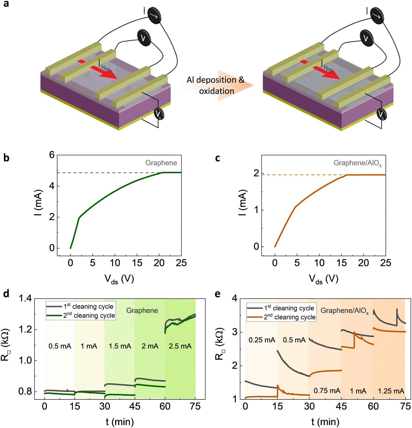 | ||
| Fig. 1 High current treatment experiments: (a) Current treatment scheme of bare graphene and graphene passivated with AlOx devices and four-probe gate dependence measurement configuration. (b) and (c) Measured four-probe I–V curves up to the high-current electrical breakdown of bare graphene and AlOx-passivated graphene devices; the dashed line indicates the electrical breakdown current. Graphene sheet resistance as a function of time for two cleaning cycles with increasing applied high-currents for (d) graphene and (e) graphene/AlOx. | ||
Bare graphene under high-current treatment
In between current-treatment steps, we performed gate-dependent measurements of four-probe channel resistance with varying applied gate voltage (VG). Fig. 2a shows the impact of the CT on a bare graphene channel. The reference curve for treatment progress is marked as no treatment. Then, graphene was under high current treatment (It) from 0.5 mA to 2.5 mA with steps (ΔIt = 0.5 mA). Between the 15 min CT spells, the gate dependence curves were measured in the range of −95 V to 20 V (Fig. 2a). Apart from obtaining electrical mobility, to gain further insights into the electrical properties of graphene and its high-current treament, we extracted the densities of trapped charge carriers (nτ) and charged impurities (ni) from gate-dependent resistance (Rch–VG) curves (Fig. S1, ESI†). The analysis reveals a decrease in trapped charge density by 3.5 × 1011 cm−2, nearly 50% change in the 1st cycle, indicating the effectiveness of the de-trapping of charges due to high current treatment (Fig. 2b). Traps and trapped charges in CVD graphene can exist at grain boundaries, impurities as well as wrinkles, which can impact electrostatic carrier tuning in graphene, and our results show that de-trapping can be done through high-current treatment. The reduction in trapped charges is significant as that creates local variations in the electrical potential, which can impede charge transport across the graphene sheet. In addition, we also found a substantial decrease in charged impurity density from 1.97 × 1012 cm−2 to 1.45 × 1012 cm−2 (Fig. 2c), which is ∼30%. While previous studies on exfoliated graphene showed a mild improvement in carrier mobility,29 in our study, for bare graphene without any coverage, we observed a gradual deterioration in carrier mobility with each step of cleaning by an overall value of ∼ 10% (Fig. 2d). Note that high current density can dislocate resist impurities and other adatom impurities through possible electromigration, and the same can also happen to carbon lattice atoms near defects and grain boundaries, which could possibly decrease the mobility of charge carriers. Thus, our results show that high current treatment of bare graphene does not necessarily enhance mobility.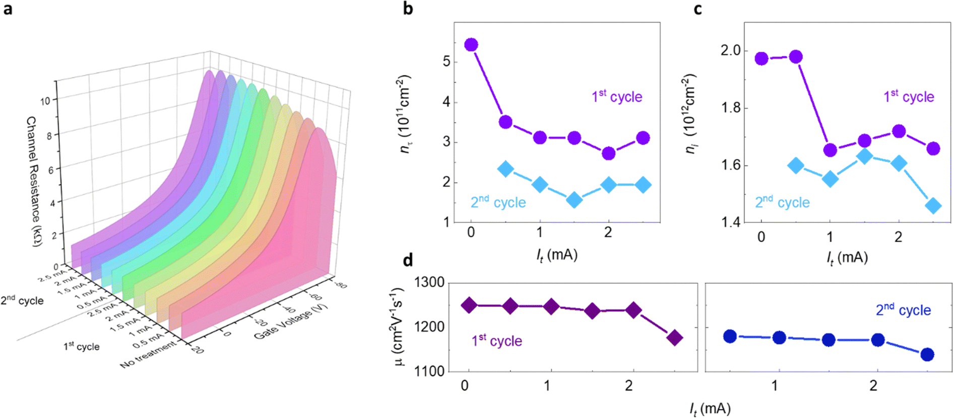 | ||
| Fig. 2 High-current treated-bare graphene: (a) Back-gate measurements in the four-probe configuration: channel resistance (Rch) as a function of the gate voltage (VG) measured with 5 μA of applied current. (b) Trapped charge density (nτ) in graphene with different current treatments (It) for two cleaning cycles. (c) Charged impurity density (ni) in graphene with different current treatments (It) for two cleaning cycles. (d) Field-effect mobility (μ) of graphene with different current treatments (It) for two cleaning cycles. The value at 0 mA is before the current treatment. | ||
High-current treated-AlOx passivated graphene (CTPG)
Having discussed the CT of bare graphene, we now focus on the impact of AlOx coverage on graphene, explored by the high-current treatment of the passivated graphene samples. To ensure the reversible (linear) regime of device operation during current treatment, the current for graphene passivated by AlOx was chosen to be two times less (It from 0.25 to 1.25 mA with ΔIt = 0.25 mA) than that used for as-fabricated graphene. Note that these values are considered from the device performance of graphene covered with AlOx (Fig. 1c). Gate dependence curves were measured after each 15-minute cleaning cycle, and it is worth noting that graphene covered with AlOx initially exhibited p-type doping.28 For this reason, a gate sweep was performed in the range of −30 to 50 V (Fig. 3a). In a manner akin to our bare graphene devices, we utilized Rch–VG curves to derive the trapped charge and charged impurity densities, understand the electrical characteristics of AlOx-passivated graphene and its behavior under high-current treatment conditions (Fig. S2, ESI†).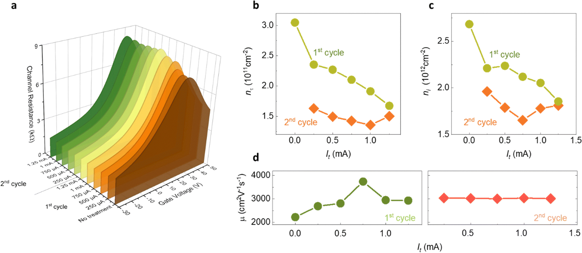 | ||
| Fig. 3 High-current treated-AlOx passivated graphene (CTPG): (a) Back-gate measurements in the four-probes configuration, channel resistance (Rch) as a function of the gate voltage (VG) measured with 5 μA of applied current. (b) Trapped charge carrier density (nτ) in graphene at different current treatments (It) for two cleaning cycles. (c) Charged impurity density (ni) in graphene at different current treatments (It) for two cleaning cycles. (d) Field-effect mobility (μ) of graphene at different current treatments (It) for two cleaning cycles. The value at 0 mA is the measurement performed before the current treatment. | ||
As displayed in Fig. 3c, our results showed that as-fabricated (without any current treatment) graphene and AlOx-passivated graphene have different levels of charged impurities 1.97 × 1012 cm−2 (Fig. 2c) and 2.7 × 1012 cm−2, respectively, with passivated graphene exhibiting nearly 30% higher impurities, which could be due to possible interface sp3 bonding caused by the top AlOx layer.28 The impact of high current on AlOx-passivated graphene is particularly interesting due to the intricate interface and the inert dielectric protection of the graphene lattice. Our study found that high current treatment or current induced cleaning (i.e. treatment) for both graphene and passivated graphene led to the same level of charged impurities ∼ 1.8–1.9 × 1012 cm−2 (Fig. 3c) after 1st cleaning cycle, indicating that this treatment can effectively reduce the number of charged impurities in both types of graphene devices to a base level. Note that the base level can be linked to the intrinsic charged impurities within the graphene lattice, for example, unsaturated bonds, that cannot be fully dislocated or neutralized, and thus the high current treatment makes the AlOx-covered graphene saturate to bare graphene charge density. The non-monotonic fluctuation of charged impurities in between individual steps seen in the 2nd cycle could be attributed to a non-linear ion removal process that could possibly occur at hot spots, such as grain boundaries and ripples, pertinent to CVD graphene. Overall, the CT leads to a 32% drop in the impurity density by the end of 2nd cycle. Similarly, this process can effectively reduce the number of charged impurities in the graphene device and subsequently decrease the number of trapped charges from 3 × 1011 cm−2 to 1.5 × 1011 cm−2 (Fig. 3b).
Strikingly, we observed a significant enhancement in the mobility of the graphene, which increased by up to 40% and stabilized at 3040 cm2 V−1 s−1 upon the first cleaning cycle (Fig. 3d). Similar improvement upon current treatment of AlOx passivated graphene was reproducibly observed on other devices in separate chips (Fig. S3, ESI†). The striking difference between bare graphene and CTPG devices upon current treatment is displayed in Fig. 4a and b, respectively. As seen here, for all bare graphene devices, the mobility decreased after high-current treatment, while the repeated enhancement in mobility up to a significant ∼ 200% in samples that initially showed low mobility. The observed increase in carrier mobility (Fig. 4b) may be attributed to the removal of impurities and defects from the surface of the graphene, as well as the modification of the underlying AlOx layer, while also improving the contact between the graphene and metal oxide layer. Additionally, surface contaminants can coalesce into larger ensembles that can be more easily removed under high currents to clean the surface effectively. It is worth noting that our devices, which have a width area of 5 μm, are large enough that any contaminants may be moved toward the edges of the device and excluded from the operation area. These results conclusively suggest that despite fabrication-induced or other interface defects, the carrier mobility in CVD graphene can be significantly enhanced via the current treatment of passivated graphene.
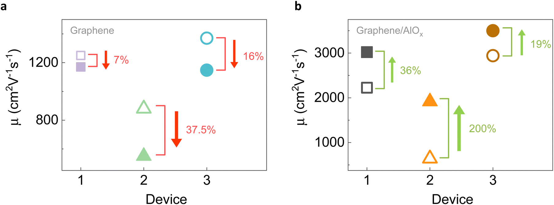 | ||
| Fig. 4 Impact of current treatment on field-effect mobility: (a) Bare graphene devices and (b) graphene/AlOx devices before (open symbols) and after current cleaning (filled symbols) with a corresponding change indicated by arrows. | ||
Investigating high-current treatment responses between graphene and passivated graphene has yielded intriguing and distinct insights. At high currents, electromigration involves two competing forces: electron wind and the macroscopic electric field. Drifting electrons transfer momentum to carbon atoms at the grain boundary or defect, causing ion migration when wind forces exceed the electric field.36 However, introducing capping layers can considerably increase the activation energy of the diffusion process, reducing stress-driven diffusion37,38 and enhancing debonding energy.39–41 In particular, for graphene, the top rigid AlOx layer imposes restrictions on the carbon atomic movements, increasing the threshold for electromigration. In addition, dipole polarization at the interface between the conducting layer and dielectric can further impact these effects. The dipole polarization occurring at the graphene/AlOx interface in a lateral structure under high current stress could lead to increased mobility of charged impurities while keeping the carbon lattice intact. The capacitive coupling between graphene and the dielectric can create a depletion region near the interface. Thus, the increase of debonding energy of carbon atoms and the dipole moment of the dielectric layer could lead to better high-current treatment impact on AlOx passivated graphene, with high interface electric field assisted preferential removal/isolation of impurities, and significantly enhancing graphene's carrier mobility. On the other hand, bare graphene (with exposed carbon atoms having a relatively lower threshold) is more prone to the electromigration of carbon atoms, which can lead to the observed deterioration of electrical mobility.
Raman-active defect passivation through current treatment on Graphene/AlOx
To understand the effectiveness of the high current treatment method and possible interface defect reduction, we conducted Raman spectroscopy analysis on both current-treated bare-graphene and graphene/AlOx samples, comparing them with the untreated channels on the same device for each case (Fig. 5a and d). Confocal Raman spectroscopy maps were obtained at a wavelength of 532 nm to determine the treatment effect by examining the D to G intensities (ID/IG) ratio along the channel and verifying the position of the graphene G and 2D peaks (Fig. S4a, ESI†). The intensity maps of the graphene channel reveal the D, G, and 2D peaks to be 1339 ± 2 cm−1, 1586 ± 1 cm−1, and 2681 ± 2 cm−1, respectively. The variation in peak position was not attributed to the channel treatment but to the local doping variation. In the case of bare graphene, the mean intensities ratio of the D to G bands (ID/IG ∼ 0.19) and 2D to G (I2D/IG ∼1.65) showed no significant change after the current treatment (Fig. 5a and b), indicating that the treatment possesses no effect on the sp3 defects (patterning of graphene by oxygen plasma could lead to edge sp3 defects) present within the channel as well as graphene quality. The Raman map of the graphene/AlOx channel closely resembled that of the bare-graphene channel, showing similar distributions of the G and 2D peaks before high current treament (Fig. S4b, ESI†). However, the positions of the D, G, and 2D peaks for the passivated graphene were identified as 1337 ± 2 cm−1, 1581 ± 2 cm−1, and 2674 ± 4 cm−1, respectively. The shift in the G peak of the graphene/AlOx compared to pristine graphene indicates p-doping caused by surface charge transfer doping.28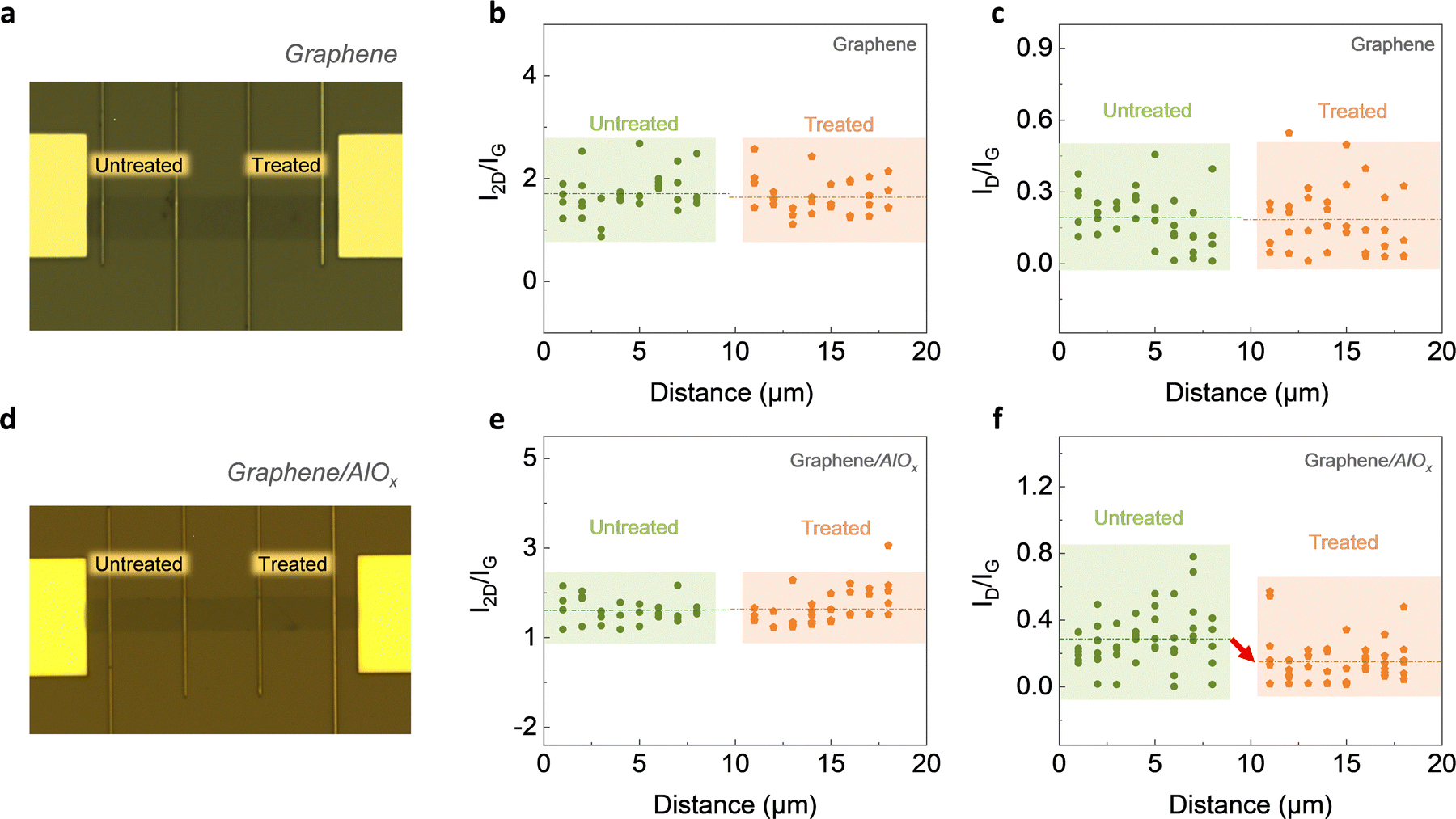 | ||
| Fig. 5 Spatially resolved Raman spectroscopy mapping: (a) Bare graphene device and measured position-dependent (b) 2D to G and (c) D to G peak intensities ratios in it with dotted lines corresponding to mean value for untreated and treated regions. (d) Graphene covered with AlOx device and measured position-dependent (e) 2D to G and (f) D to G peaks intensities ratios with dotted lines corresponding to mean value for untreated and treated regions. | ||
The analysis of the D to G intensity ratio (ID/IG) in the passivated graphene channels revealed a different response to the high current treatment (Fig. 5d). While the untreated channel exhibited a uniform cloud of data points similar to pristine graphene with a mean value of ∼ 0.28, the treated channels showed a reduction in the number of defects (Δ ∼ 0.14) and a lower distribution spread. This observation gives a striking signature of the decrease in sp3 Raman active defects with a trend toward a more standardized defect distribution along the channel. Furthermore, the 2D to G intensities ratio (mean value I2D/IG ∼ 1.2) is unaffected by current treatment in the passivated samples (Fig. 5c). These results from Raman spectroscopy are consistent with the electrical characterization, which indicated a lower density of charged impurities and an increase in mobility for graphene passivated with AlOx top layer. Thus, Raman's spectroscopy corroborates that high current treatment significantly affects the reduction of sp3 defects in graphene passivated with AlOx. Atomic force microscopy and scanning electron microscopy (Fig. S5 and S6, ESI†) show that CTPG was structurally stable, with the root mean square roughness remaining unaltered. Notably, the CTPG involving impurity electromigration is significantly different from the thermal annealing of bare graphene,42–44 which is generally applied to improving graphene quality, particularly CVD graphene grown on copper upon wet-chemical transfer onto substrates is annealed at 400 °C in argon/H2 atmosphere to remove PMMA residues. CTPG involves preserving the integrity of graphene, top oxide layer, and contacts, avoiding unnecessary diffusion, and promoting selective removal of impurities. The current treatment in the linear regime (Fig. 1b and c), with efficient heat dissipation, ensures no cumulative heating of graphene. The relatively high resistance at grain boundaries can promote higher Joule heating and can appear as hot spots with an estimated temperature rise of ∼ 10 °C per current density of 108 A cm−2 observed at the grain boundaries.45 However, in the linear regime of CT in our sample, the heat at hot spots is expected to be effectively conducted through the graphene sheet and dissipated into substrate and contacts. Overall, our results confirm that graphene passivated with AlOx can sustain and reliably respond to high high current treatment, leading to enhanced electrical performance, and thus can emerge as a solution for scalable-stable, good electronic quality graphene systems for practical applications. Note that although CVD graphene has great promise for scalability, compatibility with dry processing methods,46 and high-quality electronic and spintronic performance,35 achieving stability has been a core challenge for practical implementation. The increase in charge carrier mobility of CTPG is expected to have useful implications for developing scalable graphene electronic and spintronic device applications.
Conclusion
In summary, we demonstrated that graphene passivated with aluminum oxide (AlOx), upon subjected to high-current treatment, results in an enhanced electronic quality graphene, with an up to 200% increase in carrier mobility, compared to bare graphene, where the mobility decreases upon high-current treatment. This results from a reduced trapped charge density of 50% and a reduced charge impurity density of 30% in the passivated graphene. We confirm from Raman spectroscopy a decrease in interface sp3 defects of high-current treated-AlOx passivated graphene (CTPG), in contrast to bare graphene, which does not display any change in agreement with electrical properties. Atomic force microscopy reveals that the AlOx passivation layer remained structurally stable. In passivated graphene, an oxide layer and interface dielectric polarization can facilitate charged impurity displacement more effectively, while the dielectric layer protects the carbon atoms graphene from electromigration by enhanced debonding and activation energies. Our experiments reveal for the first time that CTPG can emerge as a reliable system for good electronic quality graphene, while the scalability of CVD graphene and the method employed here make our study an important step towards practical graphene nanoelectronic and spintronic applications.Conflicts of interest
There are no conflicts to declare.Acknowledgements
We gratefully acknowledge funding from European Research Council Consolidator Grant SPINNER (101002772), Stiftelsen Olle Engkvist Byggmästare (200–0602), Energimyndigheten (48698–1), FLAG-ERA Project MINERVA Swedish Research Council VR (2021-05932), and Formas (2019–01326, 2023-01607). M. V. K. and D. B. thank David Muradas Belinchón and Rahul Sharma for their assistance.References
- H. Mishra, J. Panda, R. Maddu, T. Sarkar, J.-F. Dayen, D. Belotcerkovtceva and M. V. Kamalakar, Experimental Advances in Charge and Spin Transport in Chemical Vapor Deposited Graphene, J. Phys. Mater., 2021, 4, 042007 CrossRef CAS.
- A. Béraud, M. Sauvage, C. M. Bazán, M. Tie, A. Bencherif and D. Bouilly, Graphene Field-Effect Transistors as Bioanalytical Sensors: Design, Operation and Performance, Analyst, 2021, 146, 403 RSC.
- Y. Wang, Y. Shao, D. W. Matson, J. Li and Y. Lin, Nitrogen-Doped Graphene and Its Application in Electrochemical Biosensing, ACS Nano, 2010, 4, 1790 CrossRef CAS PubMed.
- M. B. Lerner, F. Matsunaga, G. H. Han, S. J. Hong, J. Xi, A. Crook, J. M. Perez-Aguilar, Y. W. Park, J. G. Saven, R. Liu and A. T. C. Johnson, Scalable Production of Highly Sensitive Nanosensors Based on Graphene Functionalized with a Designed G Protein-Coupled Receptor, Nano Lett., 2014, 14, 2709 CrossRef CAS PubMed.
- F. Schedin, A. K. Geim, S. V. Morozov, E. W. Hill, P. Blake, M. I. Katsnelson and K. S. Novoselov, Detection of Individual Gas Molecules Adsorbed on Graphene, Nat. Mater., 2007, 6, 652 CrossRef CAS PubMed.
- D. A. Bandurin, D. Svintsov, I. Gayduchenko, S. G. Xu, A. Principi, M. Moskotin, I. Tretyakov, D. Yagodkin, S. Zhukov, T. Taniguchi, K. Watanabe, I. V. Grigorieva, M. Polini, G. Goltsman, A. K. Geim and G. Fedorov, Resonant Terahertz Detection Using Graphene Plasmons, Nat. Commun., 2018, 9, 1 CrossRef CAS PubMed.
- S. Schuler, J. E. Muench, A. Ruocco, O. Balci, D. van Thourhout, V. Sorianello, M. Romagnoli, K. Watanabe, T. Taniguchi, I. Goykhman, A. C. Ferrari and T. Mueller, High-Responsivity Graphene Photodetectors Integrated on Silicon Microring Resonators, Nat. Commun., 2021, 12, 3733 CrossRef CAS PubMed.
- K. Rana, J. Singh and J.-H. Ahn, A Graphene-Based Transparent Electrode for Use in Flexible Optoelectronic Devices, J. Mater. Chem. C, 2014, 2, 2646 RSC.
- C. Gréboval, U. N. Noumbé, A. Chu, Y. Prado, A. Khalili, C. Dabard, T. H. Dang, S. Colis, J. Chaste, A. Ouerghi, J. F. Dayen and E. Lhuillier, Gate Tunable Vertical Geometry Phototransistor Based on Infrared HgTe Nanocrystals, Appl. Phys. Lett., 2020, 117, 1 CrossRef.
- U. N. Noumbé, C. Gréboval, C. Livache, A. Chu, H. Majjad, L. E. Parra López, L. D. N. Mouafo, B. Doudin, S. Berciaud, J. Chaste, A. Ouerghi, E. Lhuillier and J. F. Dayen, Reconfigurable 2D/0D p-n Graphene/HgTe Nanocrystal Heterostructure for Infrared Detection, ACS Nano, 2020, 14, 4567 CrossRef PubMed.
- I. G. Serrano, J. Panda, T. Edvinsson and M. V. Kamalakar, Flexible Transparent Graphene Laminates: Via Direct Lamination of Graphene onto Polyethylene Naphthalate Substrates, Nanoscale Adv., 2020, 2, 3156 RSC.
- Q. A. Vu, H. Kim, V. L. Nguyen, U. Y. Won, S. Adhikari, K. Kim, Y. H. Lee and W. J. Yu, A High-On/Off-Ratio Floating-Gate Memristor Array on a Flexible Substrate via CVD-Grown Large-Area 2D Layer Stacking, Adv. Mater., 2017, 29, 1 CrossRef PubMed.
- Z. M. Gebeyehu, S. Parui, J. F. Sierra, M. Timmermans, M. J. Esplandiu, S. Brems, C. Huyghebaert, K. Garello, M. V. Costache and S. O. Valenzuela, Spin Communication over 30 Mm Long Channels of Chemical Vapor Deposited Graphene on SiO2, 2D Mater., 2019, 6, 1 Search PubMed.
- W. Amamou, Z. Lin, J. Van Baren, S. Turkyilmaz, J. Shi and R. K. Kawakami, Contact Induced Spin Relaxation in Graphene Spin Valves with Al2O3 and MgO Tunnel Barriers, APL Mater., 2016, 4, 1 Search PubMed.
- C. C. Lin, A. V. Penumatcha, Y. Gao, V. Q. Diep, J. Appenzeller and Z. Chen, Spin Transfer Torque in a Graphene Lateral Spin Valve Assisted by an External Magnetic Field, Nano Lett., 2013, 13, 5177 CrossRef CAS PubMed.
- L. Britnell, R. V. Gorbachev, R. Jalil, B. D. Belle, F. Schedin, A. Mishchenko, T. Georgiou, M. I. Katsnelson, L. Eaves, S. V. Morozov, N. M. R. Peres, J. Leist, A. K. Geim, K. S. Novoselov and L. A. Ponomarenko, Field-Effect Tunneling Transistor Based on Vertical Graphene Heterostructures, Science, 2012, 335, 947 CrossRef CAS PubMed.
- L. Wang, Z. Chen, C. R. Dean, T. Taniguchi, K. Watanabe, L. E. Brus and J. Hone, Negligible Environmental Sensitivity of Graphene in a Hexagonal Boron Nitride/Graphene/h-BN Sandwich Structure, ACS Nano, 2012, 6, 9314 CrossRef CAS PubMed.
- L. Viti, D. G. Purdie, A. Lombardo, A. C. Ferrari and M. S. Vitiello, HBN-Encapsulated, Graphene-Based, Room-Temperature Terahertz Receivers, with High Speed and Low Noise, Nano Lett., 2020, 20, 3169 CrossRef CAS PubMed.
- C. R. Dean, A. F. Young, I. Meric, C. Lee, L. Wang, S. Sorgenfrei, K. Watanabe, T. Taniguchi, P. Kim, K. L. Shepard and J. Hone, Boron Nitride Substrates for High-Quality Graphene Electronics, Nat. Nanotechnol., 2010, 5, 722 CrossRef CAS PubMed.
- A. S. Mayorov, R. V. Gorbachev, S. V. Morozov, L. Britnell, R. Jalil, L. A. Ponomarenko, P. Blake, K. S. Novoselov, K. Watanabe, T. Taniguchi and A. K. Geim, Micrometer-Scale Ballistic Transport in Encapsulated Graphene at Room Temperature, Nano Lett., 2011, 11, 2396 CrossRef CAS PubMed.
- M. M. Haidari, H. Kim, J. H. Kim, M. Park, H. Lee and J. S. Choi, Doping Effect in Graphene-Graphene Oxide Interlayer, Sci. Rep., 2020, 10, 1 CrossRef PubMed.
- S. Jia, H. D. Sun, J. H. Du, Z. K. Zhang, D. D. Zhang, L. P. Ma, J. S. Chen, D. G. Ma, H. M. Cheng and W. C. Ren, Graphene Oxide/Graphene Vertical Heterostructure Electrodes for Highly Efficient and Flexible Organic Light Emitting Diodes, Nanoscale, 2016, 8, 10714 RSC.
- M. Hußmann, B. Weintrub, P. Feicht, G. Germer, J. N. Kirchhof, K. I. Bolotin and S. Eigler, Controlled Assembly of Artificial 2D Materials Based on the Transfer of Oxo-Functionalized Graphene, Nanoscale Adv., 2020, 2, 176 RSC.
- H. He, S. Lara-Avila, K. H. Kim, N. Fletcher, S. Rozhko, T. Bergsten, G. Eklund, K. Cedergren, R. Yakimova, Y. W. Park, A. Tzalenchuk and S. Kubatkin, Polymer-Encapsulated Molecular Doped Epigraphene for Quantum Resistance Metrology, Metrologia, 2019, 56, 1 CrossRef.
- H. K. Seo, M. H. Park, Y. H. Kim, S. J. Kwon, S. H. Jeong and T. W. Lee, Laminated Graphene Films for Flexible Transparent Thin Film Encapsulation, ACS Appl. Mater. Interfaces, 2016, 8, 14725 CrossRef PubMed.
- Z. Wang, L. Banszerus, M. Otto, K. Watanabe, T. Taniguchi, C. Stampfer and D. Neumaier, Encapsulated Graphene-Based Hall Sensors on Foil with Increased Sensitivity, Phys. Status Solidi Basic Res., 2016, 253, 2316 CrossRef CAS.
- M. A. Giambra, A. Benfante, R. Pernice, V. Miseikis, F. Fabbri, C. Reitz, W. H. P. Pernice, R. Krupke, E. Calandra, S. Stivala, A. C. Busacca and R. Danneau, Graphene Field-Effect Transistors Employing Different Thin Oxide Films: A Comparative Study, ACS Omega, 2019, 4, 2256 CrossRef CAS PubMed.
- D. Belotcerkovtceva, R. P. MacIel, E. Berggren, R. Maddu, T. Sarkar, Y. O. Kvashnin, D. Thonig, A. Lindblad, O. Eriksson and M. V. Kamalakar, Insights and Implications of Intricate Surface Charge Transfer and Sp3-Defects in Graphene/Metal Oxide Interfaces, ACS Appl. Mater. Interfaces, 2022, 14, 36209 CrossRef CAS PubMed.
- J. Moser, A. Barreiro and A. Bachtold, Current-Induced Cleaning of Graphene, Appl. Phys. Lett., 2007, 91, 1 Search PubMed.
- R. P. Maciel, O. Eriksson, Y. O. Kvashnin, D. Thonig, D. Belotcerkovtceva, M. V. Kamalakar and C. S. Ong, Resistive Switching in Graphene: A Theoretical Case Study on the Alumina-Graphene Interface, Phys. Rev. Res., 2023, 5, 1 Search PubMed.
- V. B. Vu, J. L. Bubendorff, L. D. N. Mouafo, S. Latil, A. Zaarour, J. F. Dayen, L. Simon and Y. J. Dappe, Graphene/Aluminum Oxide Interfaces for Nanoelectronic Devices, Electron. Struct., 2023, 5, 045005 CrossRef.
- J. F. Sierra, I. Neumann, J. Cuppens, B. Raes, M. V. Costache and S. O. Valenzuela, Thermoelectric Spin Voltage in Graphene, Nat. Nanotechnol., 2018, 13, 107 CrossRef CAS PubMed.
- Y. Nam, Current Annealing Behavior in Suspended Graphene, J. Korean Phys. Soc., 2021, 79, 76 CrossRef CAS.
- J. Panda, M. Ramu, O. Karis, T. Sarkar and M. V. Kamalakar, Ultimate Spin Currents in Commercial Chemical Vapor Deposited Graphene, ACS Nano, 2020, 14, 12771 CrossRef CAS PubMed.
- D. Belotcerkovtceva, J. Panda, M. Ramu, T. Sarkar, U. Noumbe and M. V. Kamalakar, High Current Limits in Chemical Vapor Deposited Graphene Spintronic Devices, Nano Res., 2022, 16, 4233 CrossRef.
- H. B. Huntington and A. R. Grone, Current-Induced Marker Motion in Gold Wires, J. Phys. Chem. Solids, 1961, 20, 76 CrossRef CAS.
- H. Ceric and S. Selberherr, Electromigration in Submicron Interconnect Features of Integrated Circuits, Mater. Sci. Eng. R Rep., 2011, 71, 53 CrossRef.
- S. K. Lin, Y. C. Liu, S. J. Chiu, Y. T. Liu and H. Y. Lee, The Electromigration Effect Revisited: Non-Uniform Local Tensile Stress-Driven Diffusion, Sci. Rep., 2017, 7, 1 CrossRef CAS PubMed.
- H. Nakano, T. Itabashi and H. Akahoshi, Electroless Deposited Cobalt-Tungsten-Boron Capping Barrier Metal on Damascene Copper Interconnection, J. Electrochem. Soc., 2005, 152, C163 CrossRef CAS.
- C. Ryu, A. L. S. Loke, T. Nogami and S. S. Wong, Effect of Texture on the Electromigration of CVD Copper, Annu. Proc. - Reliab. Phys., 1997, 1, 201 Search PubMed.
- N. A. Lanzillo, K. Choi, C. C. Yang, K. Motoyama, H. Huang, K. Cheng, J. Maniscalco, O. Van Der Straten, C. Penny and T. Standaert, Exploring the Limits of Cobalt Liner Thickness in Advanced Copper Interconnects, IEEE Electron Device Lett., 2019, 40, 1804 CAS.
- F. Zheng, Q. H. Thi, L. W. Wong, Q. Deng, T. H. Ly and J. Zhao, Critical Stable Length in Wrinkles of Two-Dimensional Materials, ACS Nano, 2020, 14, 2137 CrossRef CAS PubMed.
- H. Sojoudi, J. Baltazar, C. Henderson and S. Graham, Impact of Post-Growth Thermal Annealing and Environmental Exposure on the Unintentional Doping of CVD Graphene Films, J. Vac. Sci. Technol., B: Nanotechnol. Microelectron.: Mater., Process., Meas., Phenom., 2012, 30, 1 Search PubMed.
- Y. Ahn, J. Kim, S. Ganorkar, Y. H. Kim and S. Il Kim, Thermal Annealing of Graphene to Remove Polymer Residues, Mater. Express, 2016, 6, 69 CrossRef CAS.
- K. L. Grosse, V. E. Dorgan, D. Estrada, J. D. Wood, I. Vlassiouk, G. Eres, J. W. Lyding, W. P. King and E. Pop, Direct Observation of Resistive Heating at Graphene Wrinkles and Grain Boundaries, Appl. Phys. Lett., 2014, 105, 1 CrossRef.
- A. Mahmood, C.-S. Yang, J.-F. Dayen, S. Park, M. V. Kamalakar, D. Metten, S. Berciaud, J.-O. Lee and B. Doudin, Room Temperature Dry Processing of Patterned CVD Graphene Devices, Carbon, 2015, 86, 256 CrossRef CAS.
Footnote |
| † Electronic supplementary information (ESI) available. See DOI: https://doi.org/10.1039/d3nh00338h |
| This journal is © The Royal Society of Chemistry 2024 |