
 Open Access Article
 This Open Access Article is licensed under a Creative Commons Attribution-Non Commercial 3.0 Unported Licence
Mechanical properties of freestanding few-layer graphene/boron nitride/polymer heterostacks investigated with local and non-local techniques†
Marcus
Lespasio‡
a,
Elena
Missale‡
 b,
Bashar
Aziz
a,
Yoosuk
Kim
a,
Giorgio
Speranza
cd,
Ralu
Divan
e,
David J.
Gosztola
e,
Chi-Hou
Lei
f,
Maria F.
Pantano
*b and
Irma
Kuljanishvili
*a
b,
Bashar
Aziz
a,
Yoosuk
Kim
a,
Giorgio
Speranza
cd,
Ralu
Divan
e,
David J.
Gosztola
e,
Chi-Hou
Lei
f,
Maria F.
Pantano
*b and
Irma
Kuljanishvili
*a
aDepartment of Physics, Saint Louis University, St. Louis, Missouri 63103, USA. E-mail: irma.kuljanishvili@slu.edu
bDepartment of Civil, Environmental and Mechanical Engineering, University of Trento, Via Mesiano 77, 38123 Trento, Italy. E-mail: maria.pantano@unitn.it
cFondazione Bruno Kessler, Via Sommarive 18, 38123 Trento, Italy
dDepartment of Industrial Engineering, University of Trento, Via Sommarive 9, 38123 Trento, Italy
eCenter for Nanoscale Materials, Argonne National Laboratory, 9700 S. Cass Avenue, Lemont, IL 60439, USA
fDepartment of Physics and Engineering, University of Scranton, Scranton, PA 18510, USA
First published on 26th September 2024
Abstract
van der Waals two-dimensional materials and heterostructures combined with polymer films continue to attract research attention to elucidate their functionality and potential applications. This study presents the fabrication and mechanical testing of 2D material heterostacks, consisting of few-layer boron nitride and graphene heterostructures synthesized via chemical vapor deposition, capped with a polymethyl methacrylate layer and suspended across ∼200 μm wide trenches using a combined wet–dry transfer method. The mechanical characterization of the heterostacks was performed using two independent approaches: (a) non-local testing with a custom-built tensile testing platform and (b) local load–displacement testing employing atomic force microscopy probes, complemented by finite element simulations. Both approaches provided new results, which are in good agreement with each other. Overall, our findings offer new insights into a combined load capacity in complex multi-material two-dimensional systems, and can contribute to advancing micro and nano-scale device designs and implementations.
1. Introduction
In the past two decades, two-dimensional (2D) van der Waals materials and their heterostructures have attracted significant interest on account of their specific characteristics, such as high aspect ratio and unique combination of physical, electrical, and mechanical properties, which make them pivotal materials for the development of novel high-performance devices.1 Indeed, since the rise of graphene (Gr), the family of 2D materials has rapidly grown, and presently includes monoelement 2D materials, like graphene, black phosphorene, and silicene, as well as bielement 2D materials, like hexagonal boron nitride (h-BN), transition metal dichalcogenides (TMDs), such as molybdenum disulfide (MoS2) or tungsten disulfide (WS2), in addition to multielement 2D materials, such as perovskites and MXenes, and heterostructures made of two or more 2D materials.2 Heterostructures are currently under consideration for a variety of applications, including metaphotonic devices,2 energy storage,3 transistors and photodiodes,4 memory,5 and photovoltaic6 devices. For example, heterostructures of h-BN and Gr are considered promising electronic systems, as h-BN has been proven to be an effective dielectric substrate material for Gr, capable of preserving its stability and electrical properties.7,8The application of 2D materials in robust devices and components relies on the knowledge of their mechanical properties.9 Given the unique size of nanomaterials, specific experimental setups are required for their mechanical characterization,10 which, in the case of films with nanoscale thickness, include buckling or bending metrology,11,12 nanoindentation,13 bulge test,14 atomic force microscopy (AFM) deflection test,15–18 and tensile test.19–22 In general, this latter technique offers the advantage of the application of more uniform stress and deformation to the sample, and can thus be preferred;23 nevertheless, it involves the manipulation of free-standing samples that can be quite challenging to achieve and often could induce damage,23 especially when relatively large area samples have to be tested, as needed in applications of industrial interest.24 In many applications, 2D materials are mounted on or capped with a polymeric substrate. The polymeric substrate, apart from facilitating 2D material manipulation, can offer several advantages, such as enabling bandgap tuning by strain engineering25 or providing an effective route to incorporate nanomaterials in polymeric matrices by piling off multiple layers, thus controlling the amount of nanomaterial while circumventing typical problems related to homogeneous filler dispersion in conventional polymer nanocomposites.24 Furthermore, other applications of polymer-coated graphene heterostructures include flexible electronics, photoelectrochemical sensors,26 electromagnetic wave absorption/detection devices,27 fuel cell membranes or nano-diffusors,28 and advanced device coatings.29
While most studies continue to employ mechanical testing of van der Waals 2D materials individually, a deep comprehension of the mechanical behaviour of heterostructures and hybrid systems is still lacking,30 especially the ones made with much larger sizes (in the order of hundreds of micrometers). Thus, expanding our understanding of the mechanical properties of hybrid systems made of 2D heterostructures, for example, Gr and BN combination, capped with a polymeric layer, is desirable and especially meaningful for practical uses, while supporting the developments of advanced materials applications.
In this study, we focus on the fabrication and mechanical characterization of large area suspended heterostacks consisting of few layer 2D heterostructures, two-three layered Gr and few-layer BN, (FLBN), capped with a sub-micrometer polymethyl methacrylate (PMMA) layer. Mechanical tests are performed using two independent approaches, including tensile tests and point-load AFM-assisted measurements, which were coupled with finite element (FE) simulations to determine the elastic modulus. Our approach effectively and independently validated consistency in using both local and non-local methods to derive the mechanical properties of large-size suspended heterostacks. To the best of our knowledge, this is the first study that directly compares local and non-local measurements to evaluate the Young's modulus of complex multilayer systems.
2. Materials and methods
2.1 Graphene and boron nitride CVD synthesis
Few layer Gr and BN films were each grown on copper (Cu) foils (25 μm thick Cu; Alpha Aesar, 99.98%) using a home-built chemical vapor deposition (CVD) system. Before growth, Cu foils were cut into 10 mm × 50 mm and cleaned in ultrasonic baths of deionized (DI) water, acetone, and isopropanol alcohol (IPA) for 5 min each, followed by nitrogen gas blow-drying.The CVD system is equipped with a three-zone furnace (Thermo Scientific Lindberg/Blue M, Waltham, MA, USA) and a quartz tube (6 ft L, 22 mm ID, 25 mm OD; Technical Glass Products, Painesville, OH, USA). A digital mass flow controller (Sierra Instrument, Monterey, CA, USA) was used to control the gas flow through the system. The prepared Cu foil was placed inside a small quartz boat and moved to the center of the quartz tube. The system was then purged with Ar gas at a flow rate of 800 sccm to reduce residual background gas. A 1 hour annealing step was then performed at 950 °C with 450 sccm of Ar and 100 sccm of H2 flowing to remove the oxide layer and further precondition the surface for the growth. To synthesize Gr, at 950 °C, a mixture of Ar/CH4 gases at a ratio of 280/15 (sccm) was flown through the system for 10 min, then CH4 gas was turned off and samples were naturally cooled down in the CVD chamber to room temperature under the protection of Ar/H2 gas flow at 450/100 sccm, respectively.
Similarly, FLBN films were prepared separately on Cu foil in the CVD system. For the FLBN film production process, 30 mg of a solid precursor of ammonia borane (NH3-BH3; Sigma Aldrich, 99.5%) was positioned 12 inches away from the Cu foil in the upstream section of the CVD quartz tube. The temperature of the precursor during BN growth was gradually increased to about 200 °C over 30 min. The evaporated precursor was carried by a mixture of Ar/H2 gases with a ratio of 300/50 (sccm) to a higher-temperature zone (990 °C) containing the Cu foil for a 40 min growth time. After growth, the samples were rapidly cooled under the flow of 450 sccm of Ar and 100 sccm of H2.26
2.2 Transfer and PMMA/Gr/BN heterostack assembly
The samples of CVD-grown Gr/Cu and FLBN/Cu were cut into square pieces of approximately 1 cm2 size. Initially, a volume of 5 μl of PMMA (495 K A4; molecular weight 495![[thin space (1/6-em)]](https://www.rsc.org/images/entities/char_2009.gif) 000) was uniformly and thinly applied across the Gr/Cu sample using a spin coater operating at 4000 rpm for 40 seconds to deposit an approximately 0.33 μm PMMA layer on top. The samples were subsequently air-dried under ambient conditions overnight. Next, the uncoated portion of the Gr on the posterior surface was eliminated using UV ozone treatment (PSD Pro Series Digital UV Ozone System) for a duration of 5 minutes. Subsequently, the PMMA/Gr/Cu sample was floated on a 2.3 M aqueous ferric chloride (FeCl3; Sigma Aldrich) bath for 24 hours in order to slowly etch the underlying copper substrate. The PMMA/Gr was then transferred from the aqueous ferric chloride bath to a clean DI water bath using an approximately 1.5 cm by 3 cm polyethylene terephthalate (PET) support beam. To do this, the PET support beam was submerged into the etching bath at an ∼45° angle using tweezers. It was then slowly raised at the same angle to carefully lift/scoop the PMMA/Gr sample out. Then, the PMMA/Gr/PET was slowly lowered again at ∼45° into the DI water bath. During this process, as the PET support beam submerges into the water, the PMMA/Gr detaches from the PET and floats on the surface of the water bath. Such water rinse procedure was repeated three times, with the PMMA/Gr sample spending 1 hour in each bath to remove residuals. Finally, the PMMA/Gr was carefully lifted from the final clean water bath with a FLBN/Cu sample using a similar technique as previously described. The resultant PMMA/Gr/FLBN/Cu stack was left to dry under ambient conditions for 24 hours. Another PMMA layer was then added on top using the same method as described before to ensure complete PMMA coverage. Next, a pre-made polydimethylsiloxane (PDMS) stamp with a trench of approximately 5 mm in diameter was affixed to the PMMA/Gr/FLBN/Cu by applying gentle pressure. The primary function of PMDS is to safeguard the sample while being transferred to a target substrate.27 The resultant PDMS/PMMA/Gr/FLBN/Cu assembly then underwent a similar Cu etch, and water rinse procedure, as previously described. Subsequently, clean PDMS/PMMA/Gr/FLBN was transferred onto a doubly pre-notched etched-in Si substrate with ∼200 μm wide and ∼50 μm deep “trenches” (ESI Fig. S1†) ensuring the PDMS and the Si substrate trenches were aligned. The heterostructure was then left to dry in ambient air for a duration of 24 hours. Finally, the sample was placed onto a hot plate (∼50 °C) for a duration of 3 min, at which point the PDMS stamp was cautiously detached, thereby releasing the PMMA/Gr/FLBN suspended heterostacks.
000) was uniformly and thinly applied across the Gr/Cu sample using a spin coater operating at 4000 rpm for 40 seconds to deposit an approximately 0.33 μm PMMA layer on top. The samples were subsequently air-dried under ambient conditions overnight. Next, the uncoated portion of the Gr on the posterior surface was eliminated using UV ozone treatment (PSD Pro Series Digital UV Ozone System) for a duration of 5 minutes. Subsequently, the PMMA/Gr/Cu sample was floated on a 2.3 M aqueous ferric chloride (FeCl3; Sigma Aldrich) bath for 24 hours in order to slowly etch the underlying copper substrate. The PMMA/Gr was then transferred from the aqueous ferric chloride bath to a clean DI water bath using an approximately 1.5 cm by 3 cm polyethylene terephthalate (PET) support beam. To do this, the PET support beam was submerged into the etching bath at an ∼45° angle using tweezers. It was then slowly raised at the same angle to carefully lift/scoop the PMMA/Gr sample out. Then, the PMMA/Gr/PET was slowly lowered again at ∼45° into the DI water bath. During this process, as the PET support beam submerges into the water, the PMMA/Gr detaches from the PET and floats on the surface of the water bath. Such water rinse procedure was repeated three times, with the PMMA/Gr sample spending 1 hour in each bath to remove residuals. Finally, the PMMA/Gr was carefully lifted from the final clean water bath with a FLBN/Cu sample using a similar technique as previously described. The resultant PMMA/Gr/FLBN/Cu stack was left to dry under ambient conditions for 24 hours. Another PMMA layer was then added on top using the same method as described before to ensure complete PMMA coverage. Next, a pre-made polydimethylsiloxane (PDMS) stamp with a trench of approximately 5 mm in diameter was affixed to the PMMA/Gr/FLBN/Cu by applying gentle pressure. The primary function of PMDS is to safeguard the sample while being transferred to a target substrate.27 The resultant PDMS/PMMA/Gr/FLBN/Cu assembly then underwent a similar Cu etch, and water rinse procedure, as previously described. Subsequently, clean PDMS/PMMA/Gr/FLBN was transferred onto a doubly pre-notched etched-in Si substrate with ∼200 μm wide and ∼50 μm deep “trenches” (ESI Fig. S1†) ensuring the PDMS and the Si substrate trenches were aligned. The heterostructure was then left to dry in ambient air for a duration of 24 hours. Finally, the sample was placed onto a hot plate (∼50 °C) for a duration of 3 min, at which point the PDMS stamp was cautiously detached, thereby releasing the PMMA/Gr/FLBN suspended heterostacks.
2.3 Characterization methods
Scanning electron microscopy (SEM) images were acquired with an FEI Inspect F50, Lausanne, Switzerland. The uniformity and integrity of Gr, FLBN, and Gr/FLBN heterostructures were evaluated using Raman spectroscopy (Renishaw, InVia, 100× objective, Wotton-under-Edge, Gloucestershire, England). Raman spectra with an excitation wavelength of 532 nm (2.33 eV) were recorded from various sample regions under ambient conditions. The Si peak at 520 cm−1 was used to reference wavenumber calibration in all Raman spectral data, and laser power was adjusted to a level below 30 mW cm−2. PMMA/Gr/FLBN thickness was evaluated using the KLA Tencor P7 Profiler. The analysis was performed across the entire sample width, from edge to edge, parallel to the geometry of the suspended material, to capture an accurate thickness profile.2.4 Tensile testing using a custom-designed mechanical platform
In order to derive the mechanical properties of the PMMA/Gr/FLBN heterostacks we used a custom-made tensile testing platform. It includes a piezoelectric linear stage to allow the application of a uniaxial displacement and a calibrated spring fabricated from a 1 mm thick polyvinyl chloride (PVC) foil to be used as a load sensor. The spring shape was chosen in order to enable sufficient deformation during the test and, thus, adequate force measurement resolution. The specimen is mounted on a doubly pre-notched Si substrate (<111> orientation), which is glued to the linear stage, on one side, and to the spring on the other side. As a result, the specimen is completely free-standing over the ∼200 μm length (the sample gauge length). Before the start of the test, the Si substrate is broken into two pieces by applying little force at one edge, while a custom-made clamp is used to keep it firmly in place.21,31 During the test, the linear stage applies increasing displacements to the end point of the sample (i.e., one of the silicon pieces) connected to the linear stage. The specimen, consequently, is stretched and transfers a part of the delivered displacement to the opposite silicon piece, thus causing a deformation of the sensor spring. Optical images are acquired during the test to record the increasing separation gap between the silicon pieces, and analysis is then performed to derive quantitative data about the displacement during the test. Next, the stress is computed as the ratio between the force measured through the load sensor spring and the sample cross-sectional area. In particular, in the present configuration, the load sensor and the specimen behave as springs in series; thus, they experience the same force, F, which can be computed as F = k·Δ, where Δ is the displacement of the sensor and k is its calibrated spring constant (5762 N m−1). Additionally, the strain is computed as the ratio between the relative displacement of the two silicon pieces and the initial sample gauge length. The thickness of the tested samples varied from 0.21 μm to 1.15 μm while the sample width varied from 1.49 mm to 3.15 mm.2.5 Point-load AFM measurements
Samples were examined by AFM (Park Systems NX 10, cantilevers with force constant ∼0.2 N m−1, resonance frequency in the range of 25 kHz, Suwon, South Korea). The tip was set to indent a total displacement of 250 nm from the sample's surface. It was brought into contact with the surface, lowered until it reached a maximum load, and then retracted. This process was conducted over 12 spots equidistant from the “trench” edges along the central axis of fully suspended heterostacks on each of 3 different samples. Parameters were set to ensure that the indent depth falls within the elastic limit of the materials. These included a maximum load limit of 80 nN and approach and retracted speeds of 2 nm s−1. In order to obtain the effective displacement, the reference displacement data recorded by the AFM were subtracted from the cantilever deflection, which was estimated as the force divided by the cantilever spring constant.2.6 Finite element analysis (FEA): simulations
ANSYS (2022 R2 Desktop Version) software was used to simulate point-load AFM measurements using finite element analysis (FEA). Given the symmetry of the problem, involving a free-standing heterostack with 1000 × 200 μm2 area and loaded at the center, a quarter model with a semi-spherical probe and suspended material of 100 μm mm width by 500 μm length was constructed with an assigned average thickness of 0.655 μm. The length and width dimensions are both halved from their experimental values to reflect the imposed symmetry conditions. Next, a fixed boundary condition was applied on the length side, which was opposite to the region of probe interaction. A (downwards) displacement of 0.2 μm was specified for the probe component, and a force reaction was set to be measured for each iteration of the simulation. Mesh refinement was adopted in the vicinity of the probe and its impacted region of the probed area of the sample. In order to compare the force–displacement data obtained from the simulations with our AFM experimental results, the force derived from the simulations was multiplied by a factor of four to account for the quarter model symmetry.3. Results and discussion
A schematic diagram of the process flow adopted for the preparation of large-area PMMA/Gr/FLBN heterostacks is shown in Fig. 1. A combination of the wet and dry transfer processes is shown in steps 1 and 2, with subsequent Cu etching and PDMS stamp release to aid an assembly of the suspended heterostack.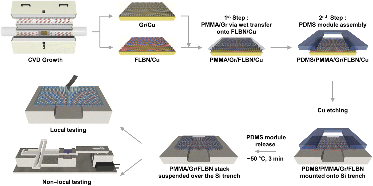 | ||
| Fig. 1 A schematic illustration of the heterostack preparation process. Gr and FLBN were grown on Cu foils by CVD. Step 1: wet transfer stacked both materials and introduced a layer of PMMA to the top. Step 2: the entire heterostack was suspended across a large etched-in Si “trench” structure using “U” shaped PDMS stamps. Non-local tensile testing and local AFM point-load testing were conducted on the transferred heterostacks. | ||
In order to assess the quality of our freestanding large area heterostacks, we used Raman spectroscopy, which is considered an essential and beneficially non-destructive approach to evaluate the properties of heterostructures and offers distinctive insights into individual materials' structural characteristics.32 For comparison, in addition to suspended heterostack samples, reference Gr/SiO2/Si, FLBN/SiO2/Si, and PMMA/SiO2/Si samples were prepared as well and analysed via Raman spectroscopy, as shown in Fig. 2.
 | ||
| Fig. 2 Raman spectroscopy characterization of the prepared Gr, FLBN, PMMA, and PMMA/Gr/FLBN heterostacks. (a) Raman spectral plots of PMMA (black), FLBN (red), and Gr (blue) transferred onto SiO2/Si substrates and PMMA/Gr/FLBN suspended heterostacks (magenta). (b) Raman spectra of PMMA/Gr/FLBN heterostacks in the 1200–1500 cm−1 region enveloped by a multi-peak (magenta solid line), and the D-band of Gr (blue), the E2g band of FLBN (red), and the PMMA peak (black) identified with Lorentz curve fitting. (c) Large-area mapping shows the G band intensity (centered at 1585 cm−1) of Gr in the suspended PMMA/Gr/FLBN heterostack; here, a white dashed line outlines the edges of the trench, (d) Raman mapping of the I2D/IG peak intensity ratio, which confirms the uniformity of the Gr. | ||
Gr exhibits characteristic Raman peaks at specific frequencies, namely D- (∼1350 cm−1), G- (∼1585 cm−1), and 2D-bands (∼2700 cm−1),33 which provide valuable information about the number of layers and structural properties. The intensity I2D/IG ratio is a quantitative indicator of the graphene's layer count. The Gr sample showed an I2D/IG ratio of around 1, indicating the presence of two-to-three-layer graphene. We expect that in large area CVD grown graphene samples layer stacking could vary from sample to sample. The full width at half maximum (FWHM) of the G-band in the Lorentzian-fitted plots for the Gr/SiO2/Si and Gr in the heterostack samples was approximately 19.87 cm−1 and 22.25 cm−1, respectively. This suggests that the Gr has high quality and crystallinity, which aligns with previous studies.33 The slightly larger value of the FWHM for the Gr G-band in the heterostack can be attributed to a broadening due to layer–layer interaction in a multilayer system. The histogram plots depicting distribution data for the intensity values for the G band from Raman mapping and I2D/IG ratio are shown in ESI Fig. S2.† Furthermore, the Raman spectrum of FLBN exhibits the E2g mode at approximately 1365 cm−1, corresponding to the characteristic Raman peak resulting from the in-plane stretching of boron and nitrogen bonds. The FWHM of this peak is 28.38 cm−1,34 as shown in Fig. 2a.
The PMMA measurement yielded three distinct peaks at 1455 cm−1, 1730 cm−1, and 2955 cm−1, as shown in Fig. 2a (black line), and is consistent with the prior research findings.35
Additionally, we performed Lorentzian fitting on Raman data from the suspended heterostack area in the range between 1200 cm−1 and 1500 cm−1, as shown in Fig. 2b. The Raman spectra acquired from these heterostacks show an overlapping of Raman peaks, generated by the PMMA peak at ∼1455 cm−1, graphene D-peak at ∼1345 cm−1, and FLBN at ∼1347 cm−1. Lorentzian multi-peak fitting shows a clearer visualization of these individual components. This evidence indicates that individual Raman signals representing different layers in the heterostack can be easily acquired, and both the structural identification and the material integrity can be effectively evaluated across the suspended region.
Additionally, Raman mapping and analyses shown in Fig. 2c and d (220 μm × 250 μm) were performed on the suspended area of the heterostack, which revealed good uniformity and homogeneity of the Gr throughout the entire 200 μm suspended region. Fig. 2d represents the Raman map of the I2D/IG ratio in the suspended area, indicating a uniform and consistent number of layers (2- to- 3 layers) across the entire suspended region. Furthermore, representative data including AFM line profiles were acquired on reference samples for FLBN/SiO2/Si and Gr/SiO2/Si as shown in ESI Fig. S3.† Some residuals left from the transfer process could be seen on the surface of each material in the AFM images, which we believe could affect the measured height profiles which show about 2.8–3.1 nm for Gr layers, and about 10–11 nm for the BN layers, measured at the perimeter edges of the sample.
In order to get insight into the mechanical properties of our PMMA/Gr/FLBN heterostacks suspended over the trenched silicon substrates, we performed tensile tests employing our custom-made platform.21,31Fig. 3a represents a photograph of our platform, while Fig. 3b depicts the representative optical image of the heterostack showing the entire suspended area.
 | ||
| Fig. 3 Tensile testing of suspended PMMA/FLBN/Gr heterostacks. (a) Custom-made tensile testing platform with functionality annotations. (b) Top view optical image of suspended heterostacks loaded onto the platform before tensile testing. (c) Resultant stress–strain plots from tensile testing data indicating characteristic mechanical behavior of suspended heterostacks. | ||
Stress–strain curves are shown in Fig. 3c. We note here two different trends present within the data set corresponding to heterostacks with different thicknesses. In particular, solid symbols represent the stress–strain curves obtained from thicker samples, which are characterized by a Young's modulus ranging from 8 to 15 GPa. Empty symbols refer instead to thinner samples, whose Young's modulus varies between 15 and 25 GPa. In addition to the Young's modulus, we determined the strength and strain at failure of our specimens, which on average resulted to be 67 ± 49 MPa and 1.7 ± 1.1%, respectively. Table 1 collects the mechanical properties derived for all tested samples. Overall, such values are in good agreement with the mechanical properties previously reported for thin graphene/PMMA nanolaminates (strength of ∼45–50 MPa, Young's modulus of ∼1.5–6 GPa, strain at failure of mostly ∼1–3%, depending on the graphene content24), yet show slightly higher Young's modulus (1–9 GPa (ref. 36)) and strength (41 ± 5 MPa (ref. 31)) but basically the same fracture strain (∼2–2.5% (ref. 37)) if compared to the data reported in the literature for PMMA films with submicrometer thickness, demonstrating that in our samples the 2D heterostructures effectively work as reinforcement components.
| Sample # | Strength [MPa] | Strain at failure [%] | Young's modulus [GPa] | Thickness [μm] |
|---|---|---|---|---|
| 1 | 35 | 4.0 | 8 | 0.62 |
| 2 | 40 | 1.9 | 15 | 0.88 |
| 3 | 32 | 0.9 | 12 | 1.00 |
| 4 | 125 | 2.1 | 15 | 0.38 |
| 5 | 40 | 1.5 | 12 | 1.15 |
| 6 | 34 | 1.3 | 11 | 0.66 |
| 7 | 160 | 1.3 | 16 | 0.34 |
| 8 | 72 | 0.5 | 25 | 0.21 |
| Average | 67 ± 49 | 1.7 ± 1.1 | 14 ± 5 | 0.65 ± 0.33 |
From the experimental data obtained for the heterostacks, we can estimate the Young's modulus (Eh) of G/BN heterostructures alone using the rule of mixtures (eqn (1)):
 | (1) |
Then, in order to get further insight into the mechanical behavior of our suspended PMMA/Gr/FLBN heterostacks and collect more reference data for direct comparison, we performed point-load AFM measurements on samples prepared from the same batch as those subjected to tensile tests. The AFM-assisted probe measurements have been shown to be a valuable method for inferring various nanomaterials' properties, including interphase mechanical properties45 and Young's modulus mapping.46 In our experiments, suspended PMMA/Gr/FLBN heterostacks transferred on the pre-notched Si-trenched substrates with the same geometry as that used for tensile tests were loaded at the middle span of their free-standing region with the tip of an AFM operated in a contact mode (C-AFM), and force–distance (F–D) data were acquired (Fig. 4). Fig. 4a shows an optical image (top view) of the cantilever in the proximity of the sample, just above the suspended region of the heterostack. Fig. 4c shows the results of the AFM measurements on three different heterostack samples (samples 9, 10, 11); here, each reported curve results from the average of twelve spots/measurements from each sample. The slope of the force–displacement curve relates to the Young's modulus of the tested sample. To translate the force–distance data into the resultant Young's modulus, we performed FEM simulations (Fig. 4b) reproducing the point-load AFM measurements and derived the Young's modulus from an iterative inverse procedure. Indeed, we set an initial value for the Young's modulus of the heterostacks, and iterations of the simulation were conducted with various input Young's modulus values until the resultant force–distance data coincided with the experimental data. Fig. 4c shows examples of the modeled force–displacement curves (Sim@14 GPa and Sim@9 GPa) obtained from simulations with the corresponding values for the Young's modulus. In particular, to reproduce the curves obtained experimentally, it emerges that the Young's modulus to be assigned to the heterostacks in the simulations falls into the range of 9–14 GPa. This range matches well the Young's modulus values derived from the tensile tests, thus proving the consistency of our approach in using both local and non-local methods to derive the mechanical properties of large-size suspended heterostacks. This represents an important result, especially if we consider that standardized methodologies are currently unavailable for the mechanical characterization of nanomaterials and ultra-thin films.10
 | ||
| Fig. 4 AFM mechanical testing and simulation for local force–displacement characterization. (a) Top view optical image of the AFM cantilever set-up over the 200 μm suspended trench. White dashed lines indicate the boundaries of the suspended material. (b) Cross-sectional quarter model schematic shows symmetry conditions (red) and displacement conditions (yellow) in the z-direction. Quarter cone (yellow) denotes the probe/tip of the cantilever. (c) Resultant force–displacement curves and obtained simulation data show an effective Young's modulus of 9 GPa to mimic sample 9's curve (solid black) and 14 GPa to mimic samples 10 (solid red) and 11's (solid blue) curves. Simulation curves for 9 GPa (green square) and 14 GPa (magenta circle) are also shown. | ||
4. Conclusions
In this work, we investigated the mechanical properties of CVD-grown large-scale, high-quality PMMA/Gr/FLBN heterostacks prepared using combined wet–dry transfer methods employing a custom designed thermal release PDMS stamp. The mechanical characterization of the heterostacks was performed with two independent methods based on local and non-local mechanical testing approaches. Non-local tensile testing employed a custom-built platform and local AFM-assisted load–displacement measurement was used to evaluate the Young's modulus of PMMA/Gr/FLBN heterostacks. From both methods, we found an overall good agreement in our results, with in situ tensile tests yielding a Young's modulus of 14 ± 5 GPa, and AFM load–displacement testing paired with FE simulation yielding values in the range of 9–14 GPa. To the best of our knowledge, mechanical properties of large-scale heterostructures capped with a polymer layer, measured by local and non-local techniques, have not been reported. Given the variety of potential applications that can be envisaged for polymer/2D material heterostacks, our findings can support future development and investigation of more complex architectures and novel devices based on such or similar heterostacks.Data availability
Required data will be available upon request.Conflicts of interest
There are no conflicts to declare.Acknowledgements
M. F. P. acknowledges support from the project “MONSTRE 2D” funded by the MIUR PRIN 2017 (Prot. 2017KFMJ8E). I. K. acknowledges support of the SLU President's Research Fund. ML acknowledges partial funding through the ILEX award from the Honors Program at Saint Louis University. Work performed at the Center for Nanoscale Materials, a U.S. Department of Energy Office of Science User Facility, was supported by the U.S. DOE, Office of Basic Energy Sciences, under Contract No. DE-AC02-06CH11357.References
- A. K. Geim and K. S. Novoselov, Nat. Mater., 2007, 6(3), 183–191 CrossRef CAS PubMed.
- H. Lin, Z. Zhang, H. Zhang, K. Te Lin, X. Wen, Y. Liang, Y. Fu, A. K. T. Lau, T. Ma, C. W. Qiu and B. Jia, Chem. Rev., 2022, 122, 15204–15355 CrossRef CAS PubMed.
- E. Pomerantseva and Y. Gogotsi, Nat. Energy, 2017, 2(7), 1–6 Search PubMed.
- Q. Zhang, L. Hou, V. Shautsova and J. H. Warner, ACS Appl. Mater. Interfaces, 2023, 15, 18012–18021 CrossRef CAS PubMed.
- F. Xue, C. Zhang, Y. Ma, Y. Wen, X. He, B. Yu, X. Zhang, F. Xue, C. Zhang, Y. Ma, Y. Wen, X. He, X. Zhang and B. Yu, Adv. Mater., 2022, 34, 2201880 CrossRef CAS PubMed.
- S. Das, D. Pandey, J. Thomas, T. Roy, S. Das, D. Pandey, J. Thomas and T. Roy, Adv. Mater., 2019, 31, 1802722 CrossRef PubMed.
- C. R. Dean, A. F. Young, I. Meric, C. Lee, L. Wang, S. Sorgenfrei, K. Watanabe, T. Taniguchi, P. Kim, K. L. Shepard and J. Hone, Nat. Nanotechnol., 2010, 5(10), 722–726 CrossRef CAS PubMed.
- L. Martini, V. Mišeikis, D. Esteban, J. Azpeitia, S. Pezzini, P. Paletti, M. W. Ochapski, D. Convertino, M. G. Hernandez, I. Jimenez and C. Coletti, ACS Appl. Mater. Interfaces, 2023, 15, 37794–37801 CrossRef CAS PubMed.
- C. Cao, S. Mukherjee, J. Liu, B. Wang, M. Amirmaleki, Z. Lu, J. Y. Howe, D. Perovic, X. Sun, C. V. Singh, Y. Sun and T. Filleter, Nanoscale, 2017, 9, 11678–11684 RSC.
- M. F. Pantano and I. Kuljanishvili, Nano Express, 2020, 1, 022001 CrossRef.
- N. Iguiñiz, R. Frisenda, R. Bratschitsch, A. Castellanos-Gomez, N. Iguiñiz, R. Frisenda, A. Castellanos-Gomez and R. Bratschitsch, Adv. Mater., 2019, 31, 1807150 CrossRef PubMed.
- M. Mezzacappa, D. Alameri, B. Thomas, Y. Kim, C. H. Lei and I. Kuljanishvili, Nanomaterials, 2022, 12, 3060 CrossRef CAS PubMed.
- K. Dey, S. Bhunia, H. S. Sasmal, C. M. Reddy and R. Banerjee, J. Am. Chem. Soc., 2021, 143, 955–963 CrossRef CAS PubMed.
- J. U. Lee, D. Yoon and H. Cheong, Nano Lett., 2012, 12, 4444–4448 CrossRef CAS PubMed.
- R. A. Soler-Crespo, L. Mao, J. Wen, H. T. Nguyen, X. Zhang, X. Wei, J. Huang, S. B. T. Nguyen and H. D. Espinosa, Matter, 2019, 1, 369–388 CrossRef.
- K. Liu, Q. Yan, M. Chen, W. Fan, Y. Sun, J. Suh, D. Fu, S. Lee, J. Zhou, S. Tongay, J. Ji, J. B. Neaton and J. Wu, Nano Lett., 2014, 14, 5097–5103 CrossRef CAS PubMed.
- A. Falin, Q. Cai, E. J. G. Santos, D. Scullion, D. Qian, R. Zhang, Z. Yang, S. Huang, K. Watanabe, T. Taniguchi, M. R. Barnett, Y. Chen, R. S. Ruoff and L. H. Li, Nat. Commun., 2017, 8(1), 1–9 CrossRef PubMed.
- T. Cui, S. Mukherjee, M. Onodera, G. Wang, B. Kumral, A. Islam, M. Shayegannia, G. Krishnan, N. Barri, P. Serles, X. Zhang, L. M. Sassi, J. Tam, N. Bassim, N. P. Kherani, P. M. Ajayan, T. Machida, C. V. Singh, Y. Sun and T. Filleter, Matter, 2022, 5, 2975–2989 CrossRef CAS.
- K. Cao, S. Feng, Y. Han, L. Gao, T. Hue Ly, Z. Xu and Y. Lu, Nat. Commun., 2020, 11(1), 1–7 CrossRef PubMed.
- Y. Yang, X. Li, M. Wen, E. Hacopian, W. Chen, Y. Gong, J. Zhang, B. Li, W. Zhou, P. M. Ajayan, Q. Chen, T. Zhu, J. Lou, Y. C. Yang, X. Li, E. Hacopian, W. B. Chen, Y. J. Gong, J. Zhang, B. Li, P. M. Ajayan, J. Lou, Q. Chen, M. R. Wen, T. Zhu and W. Zhou, Adv. Mater., 2017, 29, 1604201 CrossRef PubMed.
- M. F. Pantano, E. Missale, L. Gazzato, R. Pilot, F. Sedona, G. Speranza and M. Frasconi, Mater. Today Chem., 2022, 26, 101007 CrossRef CAS.
- Y. Yang, Z. Song, G. Lu, Q. Zhang, B. Zhang, B. Ni, C. Wang, X. Li, L. Gu, X. Xie, H. Gao and J. Lou, Nature, 2021, 594(7861), 57–61 CrossRef CAS PubMed.
- B. Wang, D. Luo, Z. Li, Y. Kwon, M. Wang, M. Goo, S. Jin, M. Huang, Y. Shen, H. Shi, F. Ding and R. S. Ruoff, Adv. Mater., 2018, 30, 1800888 CrossRef PubMed.
- C. Pavlou, M. G. Pastore Carbone, A. C. Manikas, G. Trakakis, C. Koral, G. Papari, A. Andreone and C. Galiotis, Nat. Commun., 2021, 12(1), 1–9 CrossRef PubMed.
- Z. Li, Y. Lv, L. Ren, J. Li, L. Kong, Y. Zeng, Q. Tao, R. Wu, H. Ma, B. Zhao, D. Wang, W. Dang, K. Chen, L. Liao, X. Duan, X. Duan and Y. Liu, Nat. Commun., 2020, 11(1), 1–8 CrossRef PubMed.
- G. Xiang, X. He, Y. Liu, Q. Huang, W. Huang, C. Zhang and J. Peng, ACS Appl. Mater. Interfaces, 2022, 14, 51329–51340 CrossRef CAS PubMed.
- M. Lobet, N. Reckinger, L. Henrard and P. Lambin, Nanotechnology, 2015, 26, 285702 CrossRef PubMed.
- C. N. Berger, M. Dirschka and A. Vijayaraghavan, Nanoscale, 2016, 8, 17928–17939 RSC.
- Z. Huang, A. Alharbi, W. Mayer, E. Cuniberto, T. Taniguchi, K. Watanabe, J. Shabani and D. Shahrjerdi, Nat. Commun., 2020, 11(1), 1–10 CrossRef PubMed.
- C. Androulidakis, K. Zhang, M. Robertson and S. Tawfick, 2D Mater., 2018, 5, 032005 CrossRef.
- M. F. Pantano, C. Pavlou, M. G. Pastore Carbone, C. Galiotis, N. M. Pugno and G. Speranza, ACS Omega, 2021, 6, 8308–8312 CrossRef CAS PubMed.
- L. M. Malard, M. A. Pimenta, G. Dresselhaus and M. S. Dresselhaus, Phys. Rep., 2009, 473, 51–87 CrossRef CAS.
- A. C. Ferrari, J. C. Meyer, V. Scardaci, C. Casiraghi, M. Lazzeri, F. Mauri, S. Piscanec, D. Jiang, K. S. Novoselov, S. Roth and A. K. Geim, Phys. Rev. Lett., 2006, 97, 187401 CrossRef CAS PubMed.
- R. V. Gorbachev, I. Riaz, R. R. Nair, R. Jalil, L. Britnell, B. D. Belle, E. W. Hill, K. S. Novoselov, K. Watanabe, T. Taniguchi, A. K. Geim, P. Blake, R. V Gorbachev, I. Riaz, R. R. Nair, R. Jalil, L. Britnell, B. D. Belle, E. W. Hill, K. S. Novoselov, A. K. Geim, P. Blake, K. Watanabe and T. Taniguchi, Small, 2011, 7, 465–468 CrossRef CAS PubMed.
- J. Chen, J. Li, L. Xu, W. Hong, Y. Yang and X. Chen, Polymers, 2019, 11, 601 CrossRef PubMed.
- E. Missale, M. Frasconi and M. F. Pantano, iScience, 2023, 26, 105924 CrossRef CAS PubMed.
- R. K. Bay, K. Zarybnicka, J. Jančář and A. J. Crosby, ACS Appl. Polym. Mater., 2020, 2, 2220–2227 CrossRef CAS.
- D. Davidovikj, F. Alijani, S. J. Cartamil-Bueno, H. S. J. Van Der Zant, M. Amabili and P. G. Steeneken, Nat. Commun., 2017, 8(1), 1–7 CrossRef CAS PubMed.
- A. Isacsson, A. W. Cummings, L. Colombo, L. Colombo, J. M. Kinaret and S. Roche, 2D Mater., 2016, 4, 012002 CrossRef.
- C. Lee, X. Wei, J. W. Kysar and J. Hone, Science, 2008, 321, 385–388 CrossRef CAS PubMed.
- T. Mukhopadhyay, A. Mahata, S. Adhikari and M. A. Zaeem, Sci. Rep., 2017, 7(1), 1–13 CrossRef CAS PubMed.
- P. Zhang, L. Ma, F. Fan, Z. Zeng, C. Peng, P. E. Loya, Z. Liu, Y. Gong, J. Zhang, X. Zhang, P. M. Ajayan, T. Zhu and J. Lou, Nat. Commun., 2014, 5(1), 1–7 CAS.
- L. Song, L. Ci, H. Lu, P. B. Sorokin, C. Jin, J. Ni, A. G. Kvashnin, D. G. Kvashnin, J. Lou, B. I. Yakobson and P. M. Ajayan, Nano Lett., 2010, 10, 3209–3215 CrossRef CAS PubMed.
- H. Nguyen, X. Zhang, J. Wen, X. Zhang, P. M. Ajayan and H. D. Espinosa, Mater. Today, 2023, 70, 17–32 CrossRef.
- M. Zhang, Y. Li, P. V. Kolluru and L. C. Brinson, Macromolecules, 2018, 51, 8229–8240 CrossRef CAS.
- Q. Zhu, K. Pan, S. Xie, Y. Liu and J. Li, J. Mech. Phys. Solid., 2019, 126, 76–86 CrossRef CAS.
Footnotes |
| † Electronic supplementary information (ESI) available. See DOI: https://doi.org/10.1039/d4na00514g |
| ‡ These authors contributed equally to this work. |
| This journal is © The Royal Society of Chemistry 2024 |