
 Open Access Article
 This Open Access Article is licensed under a Creative Commons Attribution-Non Commercial 3.0 Unported Licence
Defect healing and doping of CVD graphene by thermal sulfurization†
Giuseppe Valerio
Bianco
 *a,
Alberto
Sacchetti
a,
Antonella
Milella
ab,
Maria Michela
Giangregorio
a,
Stefano
Dicorato
a and
Giovanni
Bruno
a
*a,
Alberto
Sacchetti
a,
Antonella
Milella
ab,
Maria Michela
Giangregorio
a,
Stefano
Dicorato
a and
Giovanni
Bruno
a
aInstitute of Nanotechnology, CNR-NANOTEC, Dipartimento di Chimica, Università di Bari, via Orabona, 4, Bari 70126, Italy. E-mail: giuseppevalerio.bianco@cnr.it; Tel: +39-0805442082
bDipartimento di Chimica, Università di Bari, via Orabona, 4, Bari 70126, Italy
First published on 9th April 2024
Abstract
CVD graphene layers are intrinsically polycrystalline; depending on grain size, their structure at the atomic level is scarcely free of defects, which affects the properties of graphene. On the one hand, atomic-scale defects act as scattering centers and lead to a loss of carrier mobility. On the other hand, structural disorder at grain boundaries provides additional resistance in series that affects material conductivity. Graphene chemical functionalization has been demonstrated to be an effective way to improve its conductivity mainly by increasing carrier concentration. The present study reports the healing effects of sulfur doping on the electrical transport properties of single-layer CVD graphene. A post-growth thermal sulfurization process operating at 250 °C is applied on single layers of graphene on Corning-glass and Si/SiO2 substrates. XPS and Raman analyses reveal the covalent attachment of sulfur atoms in graphene carbon lattice without creating new C-sp3 defects. Measurements of transport properties show a significant improvement in hole mobility as revealed by Hall measurements and related material conductivity. Typically, Hall mobility values as high as 2500 cm2 V−1 s−1 and sheet resistance as low as 400 Ohm per square are measured on single-layer sulfurized graphene.
Introduction
Since its isolation in 2004 by Geim and Novoselov,1 graphene (“a single carbon layer of the graphite structure, describing its nature by analogy to a polycyclic aromatic hydrocarbon of quasi-infinite size”2) has attracted the attention of the scientific community because of its extraordinary properties. Among these, the strong ambipolar electric field effect allows graphene to feature very high carrier mobility. While the reputation of graphene has reached unprecedented levels, the graphene puzzle continues to be enriched with new pieces that fuel new expectations, from the point of view of fundamental scientific knowledge and industrial applications. However, over nearly 20 years, many problems regarding graphene have been solved, e.g., the optimization of CVD growth processes. However, some problems remain open and must be solved to ensure that graphene layers are further considered for increasingly sophisticated industrial applications.Significant improvements have been made on the CVD graphene growth front with the development of methodologies for (a) metal-catalyst-free direct growth on substrates,3,4 which simplifies device fabrication and prevents problems related to the graphene transfer procedure and (b) the production of single-crystal monolayer graphene, mainly through the optimization of the crystallinity of the copper catalyst,5,6 which leads to graphene exhibiting high-quality transport properties.
Regarding the healing/doping of polycrystalline graphene, which is grown with conventional CVD methodology, significant improvements have been made using various approaches, such as post-thermal annealing,7 plasma post-treatment8 and heteroatomic doping.9 It is well known that graphene preparation by CVD yields layers with defects, i.e., structural/topological and chemical defects.10–13 Depending on the specific process or methodology used, micrographically, the graphene layer appears to be composed of “individual bricks:” the grains. Grains of varying size and orientation are joined together by grain boundaries (i.e., edges), which determine most of physical and chemical properties.14–19 In particular, many studies report the role of grain boundaries in determining the overall conductivity of the graphene layer. Q. Yu et al.16 have reported interesting findings concerning the detrimental effect of the grain boundaries on electronic transport and that avoiding the grain boundaries is beneficial for improving mobility. The effectiveness of the grain boundary in affecting the electrical transport of CVD-grown polycrystalline graphene has been fingerprinted by Tsen et al.20 In their paper, they investigate how and under which circumstances the electrical transport is influenced by the grain boundaries. Surprisingly, it was found that electrical conductance may improve by one order of magnitude for the grain boundaries with better interdomain connectivity. Thus, the better the stitching among grains the better the electrical transport properties. Moreover, other topological defects, such as C-vacancies and Stone–Wales structures, wrinkles, folds, cracks and chemical defects, i.e., oxygen functional groups covalently bonded to carbon, can affect graphene properties and determine its use in technological applications.21–24
Given the crucial role of defects in determining the properties of graphene, it is important to control their formation during graphene growth and to find a way to repair existing defects. To date, many approaches have been developed to tackle this problem. Among different approaches, the reconstruction of the graphene structure, e.g., the filling of vacancies with carbon atoms from external sources and heteroatom insertion (N, B, S, and P), are reported to have the most efficient curing of defects in graphene.25–28 Importantly, the presence of grain boundaries and C-vacancy defects is essential for introducing heteroatoms in the basal plane of carbons, to tune the chemical–physical properties for specific applications.29
Among different heteroatoms, sulfur is distinct due to its “desmalusogeny” property, i.e. its ability to catenate with itself but also with carbon.30,31 A significant example is the vulcanization process in which sulphur forms cross-links between layers.32 More specifically, the crosslinking of aromatic compounds by sulphur has been deeply investigated by the H. Akamat group in the past.33 They describe how the polycyclic aromatic nuclei crosslink with each other through sulfur-bridges, which act as good electron transport paths and yield the aromaticity of the molecule.
Furthermore, theoretical works report that provided the formation energy of sulfur doping is not too high and a suitable source of sulfur atoms is used, it may be possible to synthesize sulfur-doped graphene with important changes in the electronic structure.34–36 Taking advantage of these knowledge bases, our recent research focuses on investigating the influence of sulphur doping and crosslinking on graphene. In the present paper, we report results obtained for the thermal sulfurization of CVD graphene and how the effect of sulphur insertion in the graphene basal plane on its transport properties.
Materials and methods
CVD-graphene growth and transfer
The catalytic CVD-growth methodology is as follows: graphene was grown on a 25 mm copper foil of 10 × 10 cm2 size. The copper foil was inserted into a quartz tube of the thermal-furnace CVD reactor. The quartz tube was evacuated to a vacuum better than 10−3 torr and heated to 990 °C under an H2 gas flow of 10 sccm (0.05 torr) that was maintained for 20 min after the temperature was stabilized. In the second phase, i.e., the growth phase, CH4 (5 sccm) was added to the gas feed for a growth time of 20 min. After the growth phase, the furnace was moved from the growth zone to realize the rapid cooling of the graphene/copper foil.The graphene layer was then transferred to the substrate (Corning-glass, SiO2/Si, PET) using the thermal release tape (TRtape). The sized sheet of TR-tape was applied on a piece of graphene/copper foil and pressed by a laminator. Copper was removed in an ammonium persulfate solution (20 g L−1), and the floating sheet of graphene/TR-tape was rinsed in DI water and air-dried. Graphene was directly transferred onto the substrate by hot-pressing the graphene/TR-tape (at ∼100 °C), releasing the tape.
Sulfurization process
For the thermal sulfurization process, single-layer graphene was heat treated in the presence of an excess amount of sulfur (powder 99.98%) on Corning glass and Si/SiO2 substrates in a stainless steel batch reactor (see Fig. S1 in ESI†). The process was carried out under a He inert atmosphere at a constant temperature of 230 °C for 2 h.Characterizations
The morphology of the graphene layer (in terms of grain size, wrinkles, multilayer islands and crakes) was evaluated, as done in our previous studies24,27 using optical microscopy and Raman spectroscopy. Typical grain size ranged between 50 and 200 μm2.XPS measurements were performed on as-prepared samples using a theta probe spectrometer (Thermo VG Scientific) equipped with a monochromatic Al Ka X-ray source (1486.6 eV) operated at 15 kV and a spot size of 400 mm, corresponding to a power of 70 W. Survey and high-resolution (C1s, O1s, Cl2p, and S2p) spectra were recorded in the FAT (fixed analyzer transmission) mode at pass energy of 150 and 50 eV, respectively. All spectra were acquired at a take-off angle of 37° with respect to the sample surface. A flood gun was used to balance the surface charging. The C1s signal for the sp2 graphitic component of the C1s spectrum (284.5 eV) was used as an internal standard for charging correction. The high-resolution spectra were fitted with mixed Gaussian–Lorentzian peaks after performing Shirley background subtraction. The standard deviation in the peak position was ±0.1 eV.
Raman spectra of pristine and sulfurized graphene were recorded with a LabRam HR (Horiba JY) system. All spectra were acquired at room temperature with 532 nm laser light and captured using 100× objective lens magnification with a focusing laser spot less than 1 μm in diameter. The laser power was kept at 1.0 mW to avoid the laser-induced heating effect.
The electrical properties of the graphene layers are assessed by measurements of sheet resistance, resistivity, Hall mobility and majority carrier density. The measurements are performed on a graphene layer of 1 × 1 cm2 on SiO2 (300 nm)/Si substrate. The carrier mobility is measured under a 0.3 T magnetic field at room temperature using the Hall and Van der Pauw (4-probe configuration) measurement system from MMR Technologies.
Results and discussion
The effectiveness of post-treatment for heteroatoms-doping of CVD graphene layers depends on the nature of the defects, such as carbon vacancies, topological defects (e.g. Stone–Wales defect), chemical impurities (e.g., oxygen-containing functional groups: carboxylic, carbonyl, and hydroxyl), grain size and edges. Studying the graphene treatment process with elemental sulfur offers specificity due to the peculiarity of sulfur to be able to give rise to many functionalities, especially when it interacts with condensed aromatic structures.33 The sulfurization process and S–C bond configurations in S-doped graphene (G![[thin space (1/6-em)]](https://www.rsc.org/images/entities/char_2009.gif) :S) are schematically represented in Fig. 1. Briefly, a single layer of pristine graphene, as transferred on different substrates, and sulfur molecules in the gas phase, as evaporated from the yellow sulfur powder (cyclic octatomic molecules S8), react at 230 °C to produce sulfurized graphene. It is well known that the key step in such a reaction is the opening of the S8 ring (the most abundant sulfur allotrope in the gas phase37) to form a linear biradical chain at a temperature higher than 432 K.38
:S) are schematically represented in Fig. 1. Briefly, a single layer of pristine graphene, as transferred on different substrates, and sulfur molecules in the gas phase, as evaporated from the yellow sulfur powder (cyclic octatomic molecules S8), react at 230 °C to produce sulfurized graphene. It is well known that the key step in such a reaction is the opening of the S8 ring (the most abundant sulfur allotrope in the gas phase37) to form a linear biradical chain at a temperature higher than 432 K.38
 | ||
| Fig. 1 Schematic of the sulfurization process. Top: as-prepared CVD graphene (pristine graphene) with grain boundary highlighted in blue. Bottom: graphene after sulfurization. Red represents oxygen atoms, blue is for hydrogen atoms and yellow is for sulfur atoms. Several oxygen- and sulfur-chemical functionalities are displayed. | ||
In schemes, in addition to the typical chemical functionalities of pristine CVD graphene,24 a highlight is structural defects, mainly carbon vacancies present at the grain boundaries. Let us remember that the intra-grain width may typically be in the range of 3–5 nm.19 Proposed C–S bonding configurations have been suggested by many theoretical and experimental studies, which focus on understanding the role of sulfur in relevant properties and several applications.36,39–42 Importantly, the scheme shows sulfur-bridges (–C–S–S–C–) between graphene “bricks” to be involved in a sort of vulcanization process, whereby the structure is reknit at graphene boundaries to extend, presumably, the π-electron conjugation system and, hence, the electron transport paths.39 Other sulfur-based functional groups include thiol, thiophene, thiopyran and dithiolium ring. Among these thio-polycyclic aromatic structures, the 5-atom dithiolium ring, also known as thio-thiophthen,43 has been reported to be very stable in its cationic form.36
In addition to doping graphene exclusively with sulfur by treatment with elemental sulfur, multi-heteroatom doping by SOCl2 can provide a synergistic effect for the modification of the transport properties. In a previous study on chemical doping with SOCl2, we demonstrated the presence of sulfone (C–SO2–C) and sulfoxide (C–SO–C) in the graphene structure (framework), as well as their contribution to the p-doping activity.24 Here, we also report and discuss the effectiveness of SOCl2 doping after thermal sulfurization.
To chemically fingerprint the sulfurized graphene layer and identify the S–C bonding, we performed X-ray photoelectron spectroscopy (XPS). Fig. 2 reports XPS spectra for C1s and S2p electronic states for single-layer pristine graphene after sulfur doping at 250 °C, followed by SOCl2 doping at 140 °C. Fitting of the C1s spectra of pristine graphene and S-graphene is used to identify the types of oxygen- and sulfur-containing groups. As shown in Fig. 2a, the C1s spectrum of pristine graphene can be deconvoluted into six peaks at 284.5 (1), 285.5 (2), 286.5 (3) 287.6 (4), 288.9 (5), and 290.0 eV (6) that can be associated to carbon atoms in following configurations C sp2, C–OH, C–O–C, C![[double bond, length as m-dash]](https://www.rsc.org/images/entities/char_e001.gif) O, OC–O and a shake-up peak. After sulfurization (see Fig. 2b), C1s spectrum deconvolution reveals peaks at about same energies with a slight increase in only one component. The fact that after the sulfurization process, there are no changes in the number of deconvoluted peaks, other than a little increase in the intensity of one component (2) can be interpreted as follows: sulfur atoms do not substitute oxygen atoms, but they only compensate for the regions of defects.
O, OC–O and a shake-up peak. After sulfurization (see Fig. 2b), C1s spectrum deconvolution reveals peaks at about same energies with a slight increase in only one component. The fact that after the sulfurization process, there are no changes in the number of deconvoluted peaks, other than a little increase in the intensity of one component (2) can be interpreted as follows: sulfur atoms do not substitute oxygen atoms, but they only compensate for the regions of defects.
 | ||
| Fig. 2 High-resolution (0.9 eV) C1s and S2p XPS spectra for single-layer graphene on Si/SiO2 substrates as grown (pristine graphene), after sulfurization (Graphene:S) and subsequent treatment with thionyl chloride (Graphene:S:SOCl2). (a) C1s-spectra deconvolution is performed with six peaks at 284.5 (1), 285.5 (2), 286.5 (3) 287.6 (4), 288.9 (5), 290.0 eV (6) that can be correlated to carbon atoms in following configurations: C sp2, C–OH, C–O–C, CO, OC–O and the shake-up peak. (b) C1s spectrum of Graphene:S, the deconvolution shows peaks at about same energies with only component 2 slightly increasing due to the additional contribution of C–S bond configurations. (c) and (d) S2p-spectra deconvolution of Graphene:S, after sulfurization, and subsequent treatment with SOCl2 showing the relative amount of C–S–C and C–SO2–C sulfur configurations at 164 eV and 168.3 eV, respectively. | ||
In particular, the increase in component (2) is due to the additional contribution in the C–S bond configurations. This assignment is confirmed by the analysis of the XPS S2p spectrum in Fig. 2c and d. S2p spectra show the presence of two different chemical forms: (a) the peak centred at 164 eV (resulting from the overlapping of two spin–orbit splitting peaks, 2p3/2 at 163.8 and 2p1/2 at 165.1 eV) is attributed to C–Sx–C chemical bonding in thiophene-like structures and (b) the peak at higher binding energy, centred at 168.3 eV (peak deconvolution at 168 and 169.3 eV), which is attributed to sulfone (C–SO2–C) and/or sulfoxide (C–SO–C).44,45 The predominance of (–C–Sx–C–) sulfur chemical forms is evident in graphene sulfurized with only sulfur. Following doping with SOCl2, extra sulfoxides functionalities (–C–SOx–C–) are introduced, while maintaining (–C–Sx–C–) functionalities already present in the sulfurized graphene basal plane.
Samples were also characterized by Raman spectroscopy. Fig. 3 shows a typical Raman spectrum of sulfurized graphene (S-G) extracted from Raman mapping (see linear scan map in Fig. S2†) of as-grown graphene transferred on a Si/SiO2 substrate and subjected to sulfurization by annealing at 230 °C for 2 h. For comparison, the spectra of pristine graphene before (p-G) and after annealing are also shown in an inert helium atmosphere (ann-G) for 2 hours at 230 °C without sulfur.
 | ||
| Fig. 3 Raman spectra of sulfurized single-layer graphene (G:S) on SiO2/Si (blue line) in comparison with the pristine graphene (p-G) single-layer (black line) before and after annealing (ann-G) at 230 °C (red line). | ||
For the annealed sample, in comparison with pristine graphene, 2D and G peak positions, the relative intensity ratio, and the full width at half-maximum (FWHM) do not show significant changes. However, in the low wavenumber region, the spectrum of annealed graphene shows two additional low-intensity peaks: a narrow peak centered at 1130 cm−1 and a band at 1520 cm−1. These two peaks are similar to those attributed to the presence of trans-polyenes in C-based materials.46–48 Details of the origin of these ‘‘new’’ dispersive Raman peaks have been discussed by Ferrari et al.46 and attributed to C–C and CC stretching bond vibrations in trans-polyacetylene chains, whose different lengths within the graphene sheet can also explain the dispersive behaviour. Furthermore, in our previous study,48 we discussed the reversible photothermal trans-to-cis switching of polyene. This phenomenon also occurs in the annealed sample studied here: the peaks disappear, i.e., the polyene chain switches to cis-isomer, when the annealed sample is irradiated (see Fig. S3†).
For sulfurized graphene (G:S), a comparison of p-G and ann-G showed substantial changes in spectra including the broad tail band between 1100 and 1600 cm−1,49,50 the bands of thiophene-derived Raman modes in the range 1400 to 1550 cm−1,51,52 as well as the fingerprint data of G and 2D peaks. By overlapping the spectra (see Fig. 4) that have been normalized, it is possible to better highlight variations that are observed following the treatment with sulfur and, therefore, different regions to be associated with possible C–S functionalities.
 | ||
| Fig. 4 Raman characterization demonstrating the significant change in the G peak following the sulfurization process. (a) Overlay of sulfurized graphene (G:S) with pristine graphene (p-G), which highlights the largest variation in intensity ratio I2D/IG for sulfurized graphene. (b) and (c) Detail of the G and 2D peaks, respectively, showing the shift following the sulfurization process. | ||
In the Raman spectrum of sulfurized graphene (G:S), there is cogent evidence that graphene is doped. For example, the ratio of peaks, as well as the shift in and the width of the G peaks, follow what has been described by Das et al.53 In fact, following the sulfurization process, significant changes are observed: there was a blue shift and narrowing of the G peak; the 2D/G peak intensity ratio reduced to almost one and, importantly, the intensity of the D-peak was very low (typically located at 1353 cm−1). The last observation indicates that almost negligible defect density can be caused by the structural defects generated in the layer due sulfurization process and by any possible contaminants. However, the relative shift of the G and 2D peaks shows anomalous behaviour, when compared with conventional pure-doping observations. Based on the change in the 2D/G ratio (from 2 in pristine graphene to approximately 1 in sulphur-graphene) and sharp decrease in the FWHM (from 13 cm−1 to 8 cm−1) of the G-peak, a significant blue shift of the G-peak is expected. At the same time, a blue shift of the 2D peak is anticipated, thus confirming p-doping and increase in the Fermi energy.53,54 We observe a small blue-shift of the G peak (ΔωG = 5 cm−1) and a redshift of the 2D peak (Δω2D = 3 cm−1). An important consideration to keep in mind is that the difference in electronegativity of the S and C atoms55 could be too small to promote significant charge transfer in the C–S bond configurations. Thus, the chemical doping induced by the S atoms in the π-basal plane would appear negligible. However, the inclusion of a sulfur atom, being larger than a carbon atom, especially when involved in a sulfur-bridge, can induce strain in graphene and consequently, could cause a redshift in the 2D and G Raman peaks.56 Thus, the concurrent effect of strain and increase in the Fermi energy (p-doping) can explain the anomalous variation in the 2D and G peaks shift observed after sulfurization.57
The strain can be roughly estimated, following sulfurization, by the analysis of aman peaks parameters I(2D)/I(G) and FWHM (G), which are independent of the strain; this can also be done by the position of the G and 2D peaks depending on the Fermi energy and strain.53,56. Hence, we can approximately evaluate the Fermi energy for graphene before and after sulfurization (see Fig. S5†) and further estimate the corresponding position of the G and 2D peaks for sulfurized graphene. The observed large difference in the peak position between expected and the experimental values (ΔPos(G) = 7 cm−1 and ΔPos(2D) = 13 cm−1), especially for the 2D peak confirms the existence of tensile strain of approximately 0.25%.57–59 To investigate the effect of sulfurization on the transport characteristics of graphene, we measured the Hall mobility, sheet resistance, and carrier density for single-layer graphene before and after sulfurization. Data for eight samples are shown in Fig. 5. The Hall mobility doubles going from about 1445 cm2 V−1 s−1 on average to about 2530 cm2 V−1 s−1; at the same time, the sheet resistance decreases from about 1130 Ω □−1 to about 670 Ω □−1, whereas the carrier density does not show, on average, any variation. These findings further substantiate the interpretation of Raman's fingerprint data. The increase in mobility, while maintaining constant carrier mobility, induces an increase (downwards) in the Fermi level, i.e. hole-doping and leads to observed changes in Raman features of the G and 2D peaks, as described in the above scenario (see summarized data of Raman and electrical measurements in Table S1†). The observed changes in the transport properties can be read via a simple model that essentially consists of the interrelation among Fermi energy, carrier density and Fermi velocity: 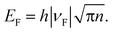 53 When we perform sulfurization, the system evolves toward higher carrier mobility and p-doping, i.e., the Fermi level moves over an amount, ΔEF, while maintaining constant hole carrier density. This can be explained by a small renormalization of the band structure that gives rise to a constricted Dirac cone shape and, consequently, increases ΔνF of Fermi velocity.
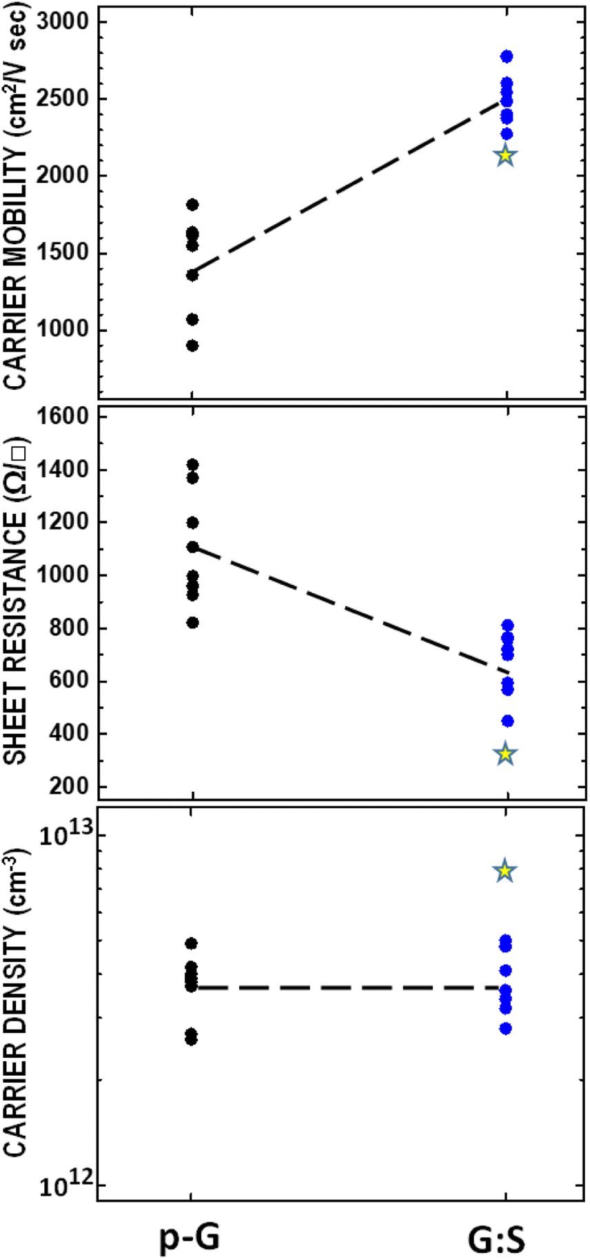 | ||
| Fig. 5 Electrical properties of pristine graphene (p-G) and sulfurized graphene (G:S) measured through a Hall device with Van der Pauw geometry (4-probe configuration). The yellow star indicates data measured on sulfurized graphene and subsequently doped with thionyl chloride (SOCl2) (the dash-dotted lines in the figures are only a guide for the eye). | ||
The observed improvement in the electrical performance of graphene upon sulfurization is also confirmed by Hall measurement performed on the sulfurized sample that had been subsequently treated with SOCl2 and whose Raman spectrum shows a further doping effect (see Fig. S4†). Typically, the sheet resistance of a single layer decreases further to 330 Ω □−1 while maintaining a high carrier mobility (see data marked with a yellow star in Fig. 5).
Conclusions
In conclusion, we have demonstrated enhancement in the electrical performance of CVD graphene on glass and SiO2 substrates by post-treatment thermal sulfurization. The presence of defects and, specifically, the grain boundaries can reduce the electrical conductivity of polycrystalline graphene. We found that using sulfur vapour at high temperatures to induce sulfur chemical reactions with graphene, sulfur is incorporated into graphene with a reknitting of the structure at the grain boundaries. Hall mobility measurements showed the hole mobility to almost double and, therefore, a decrease in the sheet resistance of sulfurized graphene occurred compared to pristine graphene at ambient conditions.The observed improvement in the electrical performance of graphene after sulfur thermal treatment is highly encouraging as it can have beneficial effects on the performance of sensors (i.e., signal intensity, detection sensitivity and response times) as well as other emerging devices.
Author contributions
G. B. conceived and designed the experiments. A. S. and G. V. B. performed the graphene growth experiments and prepared the samples. A. M. conducted the XPS investigation. G. B., A. S., M. M. G., S. D., and G. V. B. performed Raman spectroscopy and electrical measurements and analyzed the data. G. B. and G. V. B. wrote the paper. All authors discussed the results and commented on the manuscript.Conflicts of interest
The authors declare no competing interests.Acknowledgements
Funded by the European Union – NextGenerationEU, Project PRIN 2022 PNRR, cod. P20229P3JF.References
- K. S. Novoselov, A. K. Geim, S. V. Morozov, D. Jiang, Y. Zhang, S. V. Dubonos, I. V. Gregorieva and A. A. Firsov, Science, 2004, 306, 666–669 CrossRef CAS PubMed.
- (a) IUPAC Recommendations 1995, https://goldbook.iupac.org/G02683.html Search PubMed; (b) E. Fitzer, K.-H. Kochling, H. P. Boehm and H. Marsch, Pure Appl. Chem., 1995, 67, 473 CrossRef.
- A. Khan, S. M. Islam, S. Ahmed, R. R. Kumar, M. R. Habib, K. Huang, M. Hu, X. Yu and D. Yang, Adv. Sci., 2018, 5, 1800050 CrossRef.
- A. Khan, M. R. Habib, C. Jingkun, M. Xu, D. Yang and X. Yu, J. Phys. Chem. C, 2021, 125, 1774–1783 CrossRef CAS.
- Y. Zhu, J. Zhang, T. Cheng, J. Tang, H. Duan, Z. Hu, J. Shao, S. Wang, M. Wei, H. Wu, A. Li, S. Li, O. Balci, S. M. Shinde, H. Ramezani, L. Wang, L. Lin, A. C. Ferrari, B. I. Yakobson, H. Peng, K. Jia and Z. Liu, Adv. Mater., 2023, 2308802 CrossRef.
- X. Xu, Z. Zhang, J. Dong, D. Yi, J. Niu, M. Wu, L. Lin, R. Yin, M. Li, J. Zhou, S. Wang, J. Sun, X. Duan, P. Gao, Y. Jiang, X. Wu, H. Peng, R. S. Ruoff, Z. Liu, D. Yu, E. Wang, F. Ding and K. Liu, Sci. Bull., 2017, 62, 1074–1080 CrossRef CAS.
- M. B. Lee, C. T. Lee, W. W. F. Chong and K. J. Wong, J. Mater. Sci., 2023, 58, 10288–10302 CrossRef CAS.
- M. Salehi, P. Bastani, L. Jamilpanah, A. Madani, S. M. Mohseni and B. Shokri, Sci. Rep., 2021, 11, 2033 CrossRef PubMed.
- Z. W. Xian, Y. M. Chen, N. Li and T. Zhu, Analyst, 2023, 148(24), 6201–6222 RSC.
- F. Banhart, J. Kotakoski and A. V. Krasheninnikov, ACS Nano, 2011, 5, 26–41 CrossRef CAS.
- G. Yang, L. Li, W. B. Lee and M. Cheung Ng, Sci. Technol. Adv. Mater., 2018, 19, 613–648 CrossRef CAS PubMed.
- D. L. Duong, G. H. Han, F. Gunes, S. T. Kim, J. Y. Choi and Y. H. Lee, Nature, 2011, 490, 235–239 CrossRef PubMed.
- L. Jong-Young, et al. , Carbon, 2017, 115, 147–153 CrossRef.
- L. P. Birò and P. Lambin, New J. Phys., 2013, 15, 035024 CrossRef.
- O. V. Yazyev and S. G. Louie, Nat. Mater., 2010, 9, 806–809 CrossRef CAS PubMed.
- Q. Yu, L. A. Jauregui, W. Wu, R. Colby, J. Tian, Z. Su, H. Cao, Z. Liu, D. Pandey, D. Wei, T. F. Chung, P. Peng, N. P. Guisinger, E. A. Stach, J. Bao, S. S. Pei and Y. P. Chen, Nat. Mater., 2011, 10, 443–449 CrossRef CAS PubMed.
- X. Li, W. Cai, J. An, S. Kim, J. Nah, D. Yang, R. Piner, A. Velamakanni, I. Jung, E. Tutuc, S. K. Banerjee, L. Colombo and R. S. Ruoff, Science, 2009, 324, 1312–1314 CrossRef CAS.
- P. Yasaei, B. Kumar, R. Hantehzadeh, M. Kayyalha, A. Baskin, N. Repnin, C. Wang, R. F. Klie, Y. P. Chen, P. Král and A. Salehi-Khojin, Nat. Commun., 2014, 5, 4911 CrossRef CAS.
- L. Tapasztó, P. Nemes-Incze, G. Dobrik, K. J. Yoo, C. Hwang and L. P. Biró, Appl. Phys. Lett., 2012, 100, 053114 CrossRef.
- A. W. Tsen, L. Brown, M. P. Levendorf, F. Ghahari, P. Y. Huang, R. W. Havener, C. S. Ruiz-Vargas, D. A. Muller, P. Kim and J. Park, Science, 2012, 336, 1143–1146 CrossRef CAS.
- M. D. Bhatt, H. Kimab and G. Kim, RSC Adv., 2022, 12, 21520 RSC.
- W. Tian, W. Li, W. Yu and X. Liu, Micromachines, 2017, 8, 163 CrossRef.
- L. Vicarelli, S. J. Heerema, C. Dekker and H. W. Zandbergen, ACS Nano, 2015, 9(4), 3428–3435 CrossRef CAS PubMed.
- G. V. Bianco, A. Sacchetti, A. Milella, M. Grande, A. D'Orazio, P. Capezzuto and G. Bruno, Carbon, 2020, 170, 75–84 CrossRef CAS.
- J. Chen, T. Shi, T. Cai, T. Xu, L. Sun, X. Wu and D. Yu, Appl. Phys. Lett., 2013, 102, 103107 CrossRef.
- N. Chen, X. Huang and L. Qu, Phys. Chem. Chem. Phys., 2015, 17, 32077 RSC.
- G. V. Bianco, A. Sacchetti, M. Grande, A. D'Orazio, A. Milella and G. Bruno, Sci. Rep., 2022, 12, 8703 CrossRef CAS PubMed.
- L. Liu, M. Qing, Y. Wang and S. Chen, J. Mater. Sci. Technol., 2015, 31, 599–606 CrossRef CAS.
- C. Hu, D. Liu, Y. Xiao and L. Dai, Prog. Nat. Sci.: Mater. Inter., 2018, 28, 121–132 CrossRef CAS.
- G. Iurato, On Kekulé’s Insight, 2012, hal-01584824, https://hal.archives-ouvertes.fr/hal-01584824 Search PubMed.
- E. Stocchi, Chimica Organica Razionale, ed. S. E. La Prora, Milano, IT, 1964, p. 9 Search PubMed.
- J. B. Hendrickson, D. J. Cram and G. S. Hammond, Organic Chemistry, 3rd edn, McGraw-Hill, New York, 1970, p. 978 Search PubMed.
- H. Akamat, H. Inokuchi and M. Kinoshita, Carbon, 1983, 21(4), 337–343 CrossRef.
- P. A. Denis, R. Faccio and A. W. Mombru, ChemPhysChem, 2009, 10, 715–722 CrossRef CAS PubMed.
- P. A. Denis, J. Phys. Chem. C, 2009, 113, 5612–5619 CrossRef CAS.
- A. Chuvilin, E. Bichoutskaia, M. C. Gimenez-Lopez, T. W. Chamberlain, G. A. Rance, N. Kuganathan, J. Biskupek, U. Kaiser and A. N. Khlobystov, Nat. Mater., 2011, 10, 687–692 CrossRef CAS PubMed.
- J. R. Lyons, J. Sulfur Chem., 2008, 29(3–4), 269–279 CrossRef CAS.
- N. P. Tarasova, A. A. Zanin, E. G. Krivoborodov and Y. O. Mezhue, RSC Adv., 2021, 11, 9008 RSC.
- J. Xu, J. Shui, J. Wang, M. Wang, H. K. Liu, S. X. Dou, I. Y. Jeon, J.-M. Seo, J. B. Baek and L. Dai, ACS Nano, 2014, 8(10), 10920–10930 CrossRef CAS PubMed.
- Y. Liu, Y. Ma, Y. Jin, G. Chen and X. Zhang, J. Electroanal. Chem., 2015, 739, 172–177 CrossRef CAS.
- C. Bautista-Flores, J. S. Arellano-Peraza, R. Y. Sato-Berrú, E. Camps and D. Mendoza, Chem. Phys. Lett., 2016, 665, 121–126 CrossRef CAS.
- L. Yan, M. Xiao, S. Wang, D. Han and Y. Meng, J. Energy Chem., 2017, 26, 522–529 CrossRef.
- S. Bezzi, M. Mammi and C. Garbuglio, Nature, 1958, 182, 247–248 CrossRef CAS.
- H. Zhang, X. Liu, G. He, X. Zhang, S. Bao and W. Hu, J. Power Sources, 2015, 279, 252–258 CrossRef CAS.
- Z. Yang, Z. Yao, G. Li, G. Fang, H. Nie, Z. Liu, X. Zhou, X. Chen and S. Huang, ACS Nano, 2012, 6, 205–211 CrossRef CAS PubMed.
- A. C. Ferrari and J. Robertson, Phys. Rev. B: Condens. Matter Mater. Phys., 2001, 63, 121405 CrossRef.
- M. Hakamatsuka, H. Yoshimura and M. Tachibana, Carbon, 2011, 49, 1869 CrossRef CAS.
- G. Bruno, G. V. Bianco, M. M. Giangregorio, M. Losurdo and P. Capezzuto, Phys. Chem. Chem. Phys., 2014, 16, 13948 RSC.
- A. C. Ferrari, Solid State Commun., 2007, 143, 47–57 CrossRef CAS.
- J. Hong, M. K. Park, E. J. Lee, D. E. Lee, D. S. Hwang and S. Ryu, Sci. Rep., 2013, 3, 2700 CrossRef PubMed.
- F. Chen, G. Shi, J. Zhang and M. Fu, Thin Solid Films, 2003, 424, 283–290 CrossRef CAS.
- B. Kolodziejczyk, D. Mayevsky and B. Winther-Jensen, RSC Adv., 2013, 3, 4568 RSC.
- A. Das, S. Pisana, B. Chakraborty, S. Piscanec, S. K. Saha, U. V. Waghmare, K. S. Novoselov, H. R. Krishnamurthy, A. K. Geim, A. C. Ferrari and A. K. Sood, Nat. Nanotechnol., 2008, 3, 210–215 CrossRef CAS PubMed.
- M. Bruna, A. K. Ott, M. Ijas, D. Yoon, U. Sassi and A. C. Ferrari, ACS Nano, 2014, 8(7), 7432–7441 CrossRef CAS.
- E. Z. Kurmaev, A. V. Galakhov, A. Moewes, S. Moehlecke and Y. Kopelevich, Phys. Rev. B: Condens. Matter Mater. Phys., 2002, 66, 193402 CrossRef.
- T. M. G. Mohiuddin, A. Lombardo, R. R. Nair, A. Bonetti, G. Savini, R. Jalil, N. Bonini, D. M. Basko, C. Galiotis, N. Marzari, K. S. Novoselov, A. K. Geim and A. C. Ferrari, Phys. Rev. B: Condens. Matter Mater. Phys., 2009, 79, 205433 CrossRef.
- E. Lee, G. Ahn, J. Shim, Y. S. Lee and S. Ryu, Nat. Commun., 2022, 3, 1024 CrossRef.
- D. Yoon, Y. W. Son and H. Cheong, Phys. Rev. Lett., 2011, 106, 155502 CrossRef PubMed.
- J. E. Schilir, R. Lo Nigro, S. E. Panasci, F. M. Gelardi, S. Agnello, R. Yakimova, F. Roccaforte and F. Giannazzo, Carbon, 2020, 169, 172–181 CrossRef.
Footnote |
| † Electronic supplementary information (ESI) available. See DOI: https://doi.org/10.1039/d4na00124a |
| This journal is © The Royal Society of Chemistry 2024 |